EP2908230A1 - Fenêtre tactile et dispositif tactile avec celle-ci - Google Patents
Fenêtre tactile et dispositif tactile avec celle-ci Download PDFInfo
- Publication number
- EP2908230A1 EP2908230A1 EP15154882.3A EP15154882A EP2908230A1 EP 2908230 A1 EP2908230 A1 EP 2908230A1 EP 15154882 A EP15154882 A EP 15154882A EP 2908230 A1 EP2908230 A1 EP 2908230A1
- Authority
- EP
- European Patent Office
- Prior art keywords
- substrate
- sensing electrode
- touch
- disposed
- touch window
- Prior art date
- Legal status (The legal status is an assumption and is not a legal conclusion. Google has not performed a legal analysis and makes no representation as to the accuracy of the status listed.)
- Ceased
Links
Images






Classifications
-
- G—PHYSICS
- G06—COMPUTING OR CALCULATING; COUNTING
- G06F—ELECTRIC DIGITAL DATA PROCESSING
- G06F3/00—Input arrangements for transferring data to be processed into a form capable of being handled by the computer; Output arrangements for transferring data from processing unit to output unit, e.g. interface arrangements
- G06F3/01—Input arrangements or combined input and output arrangements for interaction between user and computer
- G06F3/03—Arrangements for converting the position or the displacement of a member into a coded form
- G06F3/041—Digitisers, e.g. for touch screens or touch pads, characterised by the transducing means
- G06F3/044—Digitisers, e.g. for touch screens or touch pads, characterised by the transducing means by capacitive means
- G06F3/0443—Digitisers, e.g. for touch screens or touch pads, characterised by the transducing means by capacitive means using a single layer of sensing electrodes
-
- G—PHYSICS
- G06—COMPUTING OR CALCULATING; COUNTING
- G06F—ELECTRIC DIGITAL DATA PROCESSING
- G06F3/00—Input arrangements for transferring data to be processed into a form capable of being handled by the computer; Output arrangements for transferring data from processing unit to output unit, e.g. interface arrangements
- G06F3/01—Input arrangements or combined input and output arrangements for interaction between user and computer
- G06F3/03—Arrangements for converting the position or the displacement of a member into a coded form
- G06F3/041—Digitisers, e.g. for touch screens or touch pads, characterised by the transducing means
- G06F3/0412—Digitisers structurally integrated in a display
-
- G—PHYSICS
- G06—COMPUTING OR CALCULATING; COUNTING
- G06F—ELECTRIC DIGITAL DATA PROCESSING
- G06F3/00—Input arrangements for transferring data to be processed into a form capable of being handled by the computer; Output arrangements for transferring data from processing unit to output unit, e.g. interface arrangements
- G06F3/01—Input arrangements or combined input and output arrangements for interaction between user and computer
- G06F3/03—Arrangements for converting the position or the displacement of a member into a coded form
- G06F3/041—Digitisers, e.g. for touch screens or touch pads, characterised by the transducing means
- G06F3/0416—Control or interface arrangements specially adapted for digitisers
- G06F3/04164—Connections between sensors and controllers, e.g. routing lines between electrodes and connection pads
-
- G—PHYSICS
- G06—COMPUTING OR CALCULATING; COUNTING
- G06F—ELECTRIC DIGITAL DATA PROCESSING
- G06F3/00—Input arrangements for transferring data to be processed into a form capable of being handled by the computer; Output arrangements for transferring data from processing unit to output unit, e.g. interface arrangements
- G06F3/01—Input arrangements or combined input and output arrangements for interaction between user and computer
- G06F3/03—Arrangements for converting the position or the displacement of a member into a coded form
- G06F3/041—Digitisers, e.g. for touch screens or touch pads, characterised by the transducing means
- G06F3/044—Digitisers, e.g. for touch screens or touch pads, characterised by the transducing means by capacitive means
- G06F3/0445—Digitisers, e.g. for touch screens or touch pads, characterised by the transducing means by capacitive means using two or more layers of sensing electrodes, e.g. using two layers of electrodes separated by a dielectric layer
-
- G—PHYSICS
- G06—COMPUTING OR CALCULATING; COUNTING
- G06F—ELECTRIC DIGITAL DATA PROCESSING
- G06F3/00—Input arrangements for transferring data to be processed into a form capable of being handled by the computer; Output arrangements for transferring data from processing unit to output unit, e.g. interface arrangements
- G06F3/01—Input arrangements or combined input and output arrangements for interaction between user and computer
- G06F3/03—Arrangements for converting the position or the displacement of a member into a coded form
- G06F3/041—Digitisers, e.g. for touch screens or touch pads, characterised by the transducing means
- G06F3/044—Digitisers, e.g. for touch screens or touch pads, characterised by the transducing means by capacitive means
- G06F3/0446—Digitisers, e.g. for touch screens or touch pads, characterised by the transducing means by capacitive means using a grid-like structure of electrodes in at least two directions, e.g. using row and column electrodes
-
- G—PHYSICS
- G06—COMPUTING OR CALCULATING; COUNTING
- G06F—ELECTRIC DIGITAL DATA PROCESSING
- G06F2203/00—Indexing scheme relating to G06F3/00 - G06F3/048
- G06F2203/041—Indexing scheme relating to G06F3/041 - G06F3/045
- G06F2203/04102—Flexible digitiser, i.e. constructional details for allowing the whole digitising part of a device to be flexed or rolled like a sheet of paper
-
- G—PHYSICS
- G06—COMPUTING OR CALCULATING; COUNTING
- G06F—ELECTRIC DIGITAL DATA PROCESSING
- G06F2203/00—Indexing scheme relating to G06F3/00 - G06F3/048
- G06F2203/041—Indexing scheme relating to G06F3/041 - G06F3/045
- G06F2203/04103—Manufacturing, i.e. details related to manufacturing processes specially suited for touch sensitive devices
-
- G—PHYSICS
- G06—COMPUTING OR CALCULATING; COUNTING
- G06F—ELECTRIC DIGITAL DATA PROCESSING
- G06F2203/00—Indexing scheme relating to G06F3/00 - G06F3/048
- G06F2203/041—Indexing scheme relating to G06F3/041 - G06F3/045
- G06F2203/04112—Electrode mesh in capacitive digitiser: electrode for touch sensing is formed of a mesh of very fine, normally metallic, interconnected lines that are almost invisible to see. This provides a quite large but transparent electrode surface, without need for ITO or similar transparent conductive material
Definitions
- the disclosure relates to a touch window and a touch device including the same.
- a touch panel which performs an input function through the touch to an image displayed on a touch device by an input device, such as a stylus pen or a finger, has been applied to various electronic appliances.
- the touch panel may be typically classified into a resistive touch panel and a capacitive touch panel.
- the position of the touch point is detected by detecting the variation of resistance according to the connection between electrodes when pressure is applied to an input device.
- the position of the touch point is detected by detecting the variation in capacitance when a finger of the user touches the capacitive touch panel between electrodes.
- ITO indium tin oxide
- the embodiment provides a touch window which is bendable and a display device including the same.
- a touch window includes a substrate; and a sensing electrode disposed on the substrate to sense a position, wherein the sensing electrode is disposed in a bending direction of the substrate.
- a touch device includes a display panel; and a touch window on the display panel, wherein the touch window includes a substrate; and a sensing electrode disposed on the substrate to sense a position, and wherein the sensing electrode is disposed in a bending direction of the substrate.
- compressive force may be applied to the sensing electrode when the touch window is bent.
- the sensing electrode may be bent without being subject to the physical damage as compared a case where tensile force is applied to the sensing electrode. Therefore, crack may not occur in the sensing electrode and durability of the sensing electrode may be ensured. That is, the bending property and reliability of the touch window may be improved.
- a part when referred as to be connected to the other part, the parts are not only directly connected to each other, but also indirectly connected to each other while interposing another part therebetween.
- a predetermined part when a predetermined part "includes" a predetermined component, the predetermined part does not exclude other components, but may further include other components unless otherwise indicated.
- each layer shown in the drawings may be exaggerated, omitted or schematically drawn for the purpose of convenience or clarity.
- the size of elements does not utterly reflect an actual size.
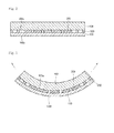
- the touch window according to an embodiment will be described in detail with reference to FIGS. 1 to 3 .
- the touch window according to an embodiment may be a curved touch window or a flexible touch window which is bendable.
- the touch window may include a cover substrate 130, a sensing electrode 200 and a wire 300.
- the cover substrate 130 may be a curved cover substrate or a flexible cover substrate which may be bent.
- the cover substrate 130 may include glass or a plastic film.
- the cover substrate 130 may include tempered glass, semi-tempered glass, soda lime glass, reinforced plastic, or flexible plastic.
- the chemically tempered glass includes glass which is chemically tempered.
- the chemically tempered glass may include soda lime glass or aluminosilicate glass.
- the cover substrate 130 may have a predetermined strength to protect the sensing electrode 200 and the wire 300.
- the cover substrate 130 may include an active area AA and an unactive area UA.
- the active area AA refers to an area through which a touch instruction may be input by a user.
- the unactive area UA refers to an area to which the touch instruction is not input because the unactive area UA is not activated even if the touch of the user is input thereto.
- a substrate 100 may be disposed under the cover substrate 130.
- the substrate 100 may support the sensing electrode and the wire formed on the substrate 100.
- the substrate 100 may include reinforced plastic or flexible plastic, such as polyimide (PI), polyethylene terephthalate (PET), propylene glycol (PPG) or polycarbonate (PC), or may include sapphire.
- the substrate 100 may include an optical isotropic film.
- the substrate 100 may include cyclic olefin copolymer (COC), cyclic olefin polymer (COP), optical isotropic polycarbonate (PC), or optical isotropic polymethyl methacrylate (PMMA).
- COC cyclic olefin copolymer
- COP cyclic olefin polymer
- PC optical isotropic polycarbonate
- PMMA optical isotropic polymethyl methacrylate
- the sapphire has superior electric characteristics, such as permittivity, so that a touch response speed may be greatly increased and a space touch such as hovering may be easily implemented.
- the sapphire has a high surface hardness
- the sapphire is applicable to a cover substrate.
- the hovering signifies a technique for recognizing a coordinate even in a position spaced apart from a display by a short distance.
- the embodiment is not limited thereto, and the substrate 100 may include various materials to form the sensing electrode and the wire.
- the substrate 100 may be a curved substrate or a flexible substrate which may be bent.
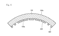
- the substrate 100 may include a first surface 100a and a second substrate 100b opposite to the first surface 100a.
- the first surface 100a may be combined with the cover substrate 130.
- the substrate 100 may be bent inward about the first surface 100a.
- the first surface 100a of the substrate 100 may be compressed and the second surface 100b of the substrate 100 may be expanded.
- the sensing electrode 200 may be disposed on the active area AA of the substrate 100.
- the sensing electrode 200 disposed on the active area AA may serve as a sensor for sensing a touch.
- the sensing electrode 200 may be disposed on the first surface 100a of the substrate 100. That is, the sensing electrode 200 may be disposed along the bending direction of the substrate 100. The sensing electrode 200 may be disposed on a compressed surface of the substrate 100.
- the length of the sensing electrode may be shortened as compared with the original length thereof.
- the sensing electrode may be bent without being subject to the physical damage as compared with a case where tensile force is applied to the sensing electrode. Therefore, crack may not occur in the sensing electrode and durability of the sensing electrode may be ensured. That is, the bending property and reliability of the touch window may be improved.
- bridge electrodes 230 may be disposed on the active area AA.
- a first sensing electrode 210 extending in one direction and a second sensing electrode 220 extending in the other direction may be disposed on the active area AA.
- the bridge electrode 230 and the sensing electrode 200 may include a transparent conductive material which allows electricity to flow therethrough without interfering with light transmission.
- the bridge electrode 230 and the sensing electrode 200 may include metal oxide, such as indium tin oxide, indium zinc oxide, copper oxide, tin oxide, zinc oxide, or titanium oxide.
- the bridge electrode 230 and the sensing electrode 200 may include a nanowire, a photosensitive nanowire film, carbon nanotube (CNT), graphene, conductive polymer or a mixture thereof.
- CNT carbon nanotube
- the sensing electrode 2010 may include at least one of Cr, Ni, Cu, Al, Ag, Mo, and an alloy thereof.
- the bridge electrode 230 and the sensing electrode 200 may include the same material or mutually different materials.
- the sensing electrode 200 having a rhombus shape is shown in the drawings, the embodiment is not limited thereto.
- the sensing electrode 200 may have various shapes, such as a polygonal shape including a triangular shape or a rectangular shape, a circular shape, a linear shape, an H shape or an oval shape.
- the bridge electrodes 230 may have a bar shape.
- the bridge electrodes 230 having the bar shape are disposed on the active area AA while being spaced apart from each other by a regular interval.
- the bridge electrodes 230 may serve as connection electrodes for the first sensing electrode 210.
- capacitance variation may occur at a touch position, so that the touch position may be detected based on the capacitance variation.
- a printing layer 500 is disposed on the unactive area UA.
- the printing layer 500 may extend along an edge of the substrate 100.
- the printing layer 500 may be formed through one-color printing, two-color printing or three-color printing.
- the printing layer 500 may represent black or white by coating black ink or white ink according to the desired outer appearance thereof.
- the printing layer 500 may represent various colors, such as red or blue, by using various color films.
- the printing layer 500 may have at least one layer. For instance, the printing layer 500 may be prepared as a single layer or as at least two layers having widths different from each other.
- the printing layer 500 may be formed of a film. If the substrate is flexible or has a curvature, it is difficult to form the printing layer on the cover substrate 130. In this case, the printing layer is formed on the film and then the film is formed on the curved or flexible cover substrate to facilitate the manufacturing process.
- the film may include an optical isotropic film.
- the printing layer 500 may be formed on a side of the substrate, which is adjacent to the cover substrate, or on another side of the substrate which is opposite to the cover substrate.
- the printing layer 500 may cover the wire 300, which will be described later, such that the wire 300 cannot be viewed from the outside.
- a pattern may be formed on the printing layer 500 to realize a desired logo.
- the wire 300 may be formed on the unactive area UA to electrically connect the sensing electrode 200.
- One end of the wire 300 may be connected to the sensing electrode 200 and the other end of the wire 300 may be connected to a printed circuit board.
- the wire 300 is connected to the sensing electrode 200 and drawn to an upper end or a lower end of the substrate 100.
- a pad part is disposed on the other end of the wire 300 and connected to the printed circuit board.
- the wire 300 may be formed of metal having superior electric conductivity.
- the wire 300 may include chrome (Cr), nickel (Ni), copper (Cu), aluminum (Al), silver (Ag), molybdenum (Mo), and an alloy thereof.
- the wire 300 may include various metal paste materials which can be formed through a printing process.
- Various types of printed circuit board can be employed.
- a flexible printed circuit board FPCB
- FPCB flexible printed circuit board
- an adhesive layer may be disposed between the cover substrate 130 and the substrate 100.
- the adhesive layer may include optical clear adhesive (OCA) or a photoresist film.
- FIGS. 4 and 5 For the purpose of clarity and simplicity, detailed description about the same or similar elements or parts, which have already been described above, will be omitted.
- the substrate 100 is disposed under the cover substrate 130 and the second surface 100b of the substrate 100 may be combined with the cover substrate 130.
- the sensing electrode 200 is disposed on the first surface 100a of the substrate and the substrate 100 may be bent inward about the first surface 100a.
- the sensing electrode may also be disposed on the cover substrate 130.
- the cover substrate 130 of the touch window may include a first surface 130a and a second surface 130b, which are opposite to each other, and the sensing electrode 200 may be directly disposed on the cover substrate 130.
- the cover substrate 130 is bent inward about the first surface 130a and the sensing electrode 200 may be disposed on the first surface 130a.
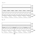
- the substrate 100 of the touch window includes a first substrate 110 and a second substrate 120.
- a first sensing electrode 210 may be disposed on the first substrate 110 and a second sensing electrode 220 may be disposed on the second substrate 120.
- the first substrate 110 may include a first surface 110a and a second surface 110b, which are opposite to each other.
- the first surface 110a may be combined with the second substrate 120.
- the first substrate 110 may be bent inward about the first surface 110a.
- the first surface 110a of the first substrate 110 may be compressed and the second surface 110b of the first substrate 110 may be expanded.
- the first sensing electrode 210 may be disposed on the first surface 110a of the first substrate 110.
- the second substrate 120 may include a first surface 120a and a second surface 120b, which are opposite to each other.
- the first surface 120a may be combined with the cover substrate 130.
- the second substrate 120 may be bent inward about the first surface 120a.
- the first surface 120a of the second substrate 120 may be compressed and the second surface 120b of the second substrate 120 may be expanded.
- the second sensing electrode 220 may be disposed on the first surface 120a of the second substrate 120.
- first and second substrates 110 and 120 may include mutually different materials.
- the second substrate 120 may include a dielectric material.
- the second substrate 120 may have a thickness thinner than a thickness of the first substrate 110.
- the second substrate 120 may be directly formed on the top surface of the first substrate 110. That is, the second substrate 120 may be formed by directly applying the dielectric material on the top surface of the first substrate 110. Then, the second sensing electrode 220 may be formed on the second substrate 120.
- an additional adhesive layer may not be necessary between the second substrate 120 and the first substrate 110, so that the thickness can be reduced as compared with the structure using two film substrates.
- the second surface 110b of the first substrate 110 may be combined with the second substrate 120.
- the second surface 120b of the second substrate 120 may be combined with the cover substrate 130.
- the touch window may include the cover substrate 130 and the substrate 110.
- the second sensing electrode 220 may be disposed on the cover substrate 130 and the first sensing electrode 210 may be disposed on the substrate 110.
- the cover substrate 130 may include a first surface 130a and a second surface 130b, which are opposite to each other.
- the first surface 130a may be combined with the substrate 110.
- the cover substrate 130 may be bent inward about the first surface 130a.
- the first surface 130a of the cover substrate 130 may be compressed and the second surface 130b of the cover substrate 130 may be expanded.
- the second sensing electrode 220 may be disposed on the first surface 130a of the cover substrate 130.
- the substrate 110 may include a first surface 110a and a second surface 110b, which are opposite to each other.
- the second surface 110b may be combined with the cover substrate 130.
- the substrate 110 may be bent inward about the first surface 110a.
- the first surface 110a of the substrate 110 may be compressed and the second surface 110b of the substrate 110 may be expanded.
- the first sensing electrode 210 may be disposed on the first surface 110a of the substrate 110.
- the first and second electrodes 210 and 220 may include a conductive pattern. That is, the first and second electrodes 210 and 220 may be disposed in a mesh shape.
- the first and second electrodes 210 and 220 may include a pattern opening OA and a pattern line LA.
- a line width of the pattern line LA may be in the range of 0.1 ⁇ m to 10 ⁇ m.
- the pattern LA having a line width of 0.1 ⁇ m or less may not be formed through the manufacturing process or may cause short circuit. If the line width excesses 10 ⁇ m, the electrode pattern may be viewed from the outside, thereby deteriorating the visibility.
- the line width of the pattern line LA may be in the range of about 0.5 ⁇ m to about 7 ⁇ m. More preferably, the line width of the pattern line LA may be in the range of about 1 ⁇ m to about 3.5 ⁇ m.
- the pattern opening OA may have various shapes.
- the pattern opening OA may have a polygonal shape including a rectangular shape, a diamond shape, a pentagonal shape or a hexagonal shape, or a circular shape.
- the pattern opening OA may have a regular shape or a random shape.
- the embodiment is not limited to the above.
- the conductive pattern opening may have an irregular shape. That is, the conductive pattern opening having various shapes may be formed in one conductive pattern.
- the electrode 200 may include the conductive pattern opening having various shapes.
- the pattern of the first and second electrodes 210 and 220 may not be viewed in a display area. In other words, even when the first and second electrodes 210 and 220 are formed of metal, the pattern may not be viewed. In addition, even when the first and second electrodes 210 and 220 are applied to a large-size touch window, the resistance of the touch window may be reduced. Further, when the first and second electrodes 210 and 220 are formed through a printing process, the printing quality may be improved, so that the high-quality touch window may be secured.
- the touch device may include the touch panel disposed on a display panel 600.
- the touch device may be prepared by coupling the cover substrate 130 with the display panel 600.
- the cover substrate 130 and the display panel 600 may be bonded to each other through an adhesive layer 700.
- the cover substrate 130 may be combined with the display panel 600 by the adhesive layer 700 including the optical clear adhesive (OCA).
- OCA optical clear adhesive
- the touch device when the substrate 100 is further disposed on the cover substrate 130, the touch device may be prepared by coupling the substrate 100 with the display panel 600.
- the substrate 100 and the display panel 600 may be bonded to each other through the adhesive layer 700.
- the substrate 100 may be combined with the display panel 600 by the adhesive layer 700 including the optical clear adhesive (OCA).
- OCA optical clear adhesive
- the display panel 600 may include a first substrate 610 and a second substrate 620.
- the display panel 600 may have a structure in which the first substrate 610 including a thin film transistor (TFT) and a pixel electrode is combined with the second substrate 620 including color filter layers while a liquid crystal layer is interposed between the first and second substrates 610 and 620.
- TFT thin film transistor
- the display panel 600 may be a liquid crystal display panel having a color filter on transistor (COT) structure formed by combining the first substrate 610, which is formed thereon with the TFT, a color filter, and a black matrix, with the second substrate 620 while the liquid crystal layer is interposed between the first and second substrates 610 and 620.
- the TFT may be formed on the first substrate 610
- a protective layer may be formed on the TFT
- the color filter layer may be formed on the protective layer.
- the pixel electrode which makes contact with the TFT, may be formed on the first substrate 610.
- the black matrix may be omitted, and a common electrode may perform a function of the black matrix together with the inherent function thereof.
- the display device may further include a backlight unit for supplying light onto a rear surface of the display panel 600.
- the display panel 600 When the display panel 600 is an organic electroluminescence light emitting device, the display panel 600 includes self-luminescence device which does not require any additional light source.
- a thin film transistor is formed on the first substrate 610 of the display panel 600, and an organic light-emitting device making contact with the thin film transistor is formed.
- the organic light-emitting device may include an anode, a cathode and an organic light-emitting layer formed between the anode and the cathode.
- the display panel 600 may further include the second substrate 620, which performs the function of an encapsulation substrate for encapsulation, on the organic light-emitting device.
- the touch device may include a touch panel integrated with the display panel 600. That is, a substrate for supporting at least one sensing electrode may be omitted.
- At least one sensing electrode may be disposed on at least one surface of the display panel 600. That is, at least one sensing electrode may be disposed on one surface of at least one of the first and second substrates 610 and 620.
- At least one sensing electrode may be formed on the top surface of the substrate positioned at an upper portion.
- the first sensing electrode 210 may be disposed on one surface of the cover substrate 100. In addition, the first wire connected to the first sensing electrode 210 may be disposed. Further, the second sensing electrode 220 may be disposed on one surface of the display panel 600. In addition, the second wire connected to the second sensing electrode 220 may be disposed.
- the adhesive layer 700 may be disposed between the cover substrate 100 and the display panel 600 to combine the cover substrate 100 with the display panel 600.
- a polarizing plate may be disposed under the cover substrate 100.
- the polarizing plate may be a linear polarizing plate or an anti-reflection polarizing plate.
- the polarizing plate may be a linear polarizing plate.
- the polarizing plate may be an anti-reflection polarizing plate.
- the touch device according to the embodiment may allow at least one substrate supporting the sensing electrode to be omitted. For this reason, a touch device having a thin thickness and a light weight may be formed.
- the touch device may include a touch window integrated with a display panel 600. That is, a substrate for supporting at least one sensing electrode may be omitted.
- a sensing electrode which serves as a sensor disposed in an active area to sense a touch
- a wire through which an electrical signal is applied to the sensing electrode
- at least one sensing electrode or at least one wire may be disposed inside the display panel.
- the display panel 600 includes first and second substrates 610 and 620.
- at least one of the first and second electrodes 210 and 220 is disposed between the first and second substrates 610 and 620. That is, at least one sensing electrode may be formed on at least one surface of the first or second substrate 610 or 620.
- the first sensing electrode 210 may be formed on one surface of the cover substrate 100.
- the first wire connected to the first sensing electrode 210 may be disposed.
- the second sensing electrode 220 and the second wire may be formed between the first and second substrates 610 and 620. That is, the second sensing electrode 220 and the second wire may be disposed inside the display panel, and the first sensing electrode 210 and the first wire may be disposed outside the display panel.
- the second sensing electrode 220 and the second wire may be disposed on the top surface of the first substrate 610 or the rear surface of the second substrate 620.
- a polarizing plate may be further disposed under the cover substrate 100.
- the sensing electrode may be formed with a thin film transistor (TFT) and a pixel electrode.
- TFT thin film transistor
- a color filter layer may be formed on the sensing electrode or the sensing electrode may be formed on the color filter layer.
- the sensing electrode may be formed with a thin film transistor or an organic light emitting device.
- the touch device according to the embodiment may allow an additional substrate supporting the sensing electrode to be omitted. For this reason, the touch device having a thin thickness and a light weight may be formed.
- the process can be simplified and the cost can be saved by forming the sensing electrode and the wire together with the device formed on the display panel.
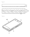
- the mobile terminal may include an active area AA and an unactive area UA.
- the active area AA may sense a touch signal through the touch by a finger, and a command icon pattern part and a logo may be formed in the unactive area UA.
- the touch window may include a flexible touch window that is bendable.
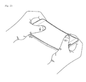
- the touch device including the touch window may be a flexible touch device. Therefore, a user can curve or bend the flexible touch window with a hand.
- Such a flexible touch window may be implemented for a wearable touch.
- the touch window may be applied to a vehicle navigation system as well as the touch device of a mobile terminal.
- the touch window may be applied to an inner part of a vehicle.
- the touch window may be applied to various parts in the vehicle.
- the touch window may be applied to a dashboard as well as a PND (Personal Navigation Display), so that a CID (Center Information Display) may be realized.
- the embodiment is not limited to the above, and the display device may be used for various electronic appliances.
- any reference in this specification to "one embodiment,” “an embodiment,” “example embodiment,” etc. means that a particular feature, structure, or characteristic described in connection with the embodiment is included in at least one embodiment of the invention.
- the appearances of such phrases in various places in the specification are not necessarily all referring to the same embodiment.
Landscapes
- Engineering & Computer Science (AREA)
- General Engineering & Computer Science (AREA)
- Theoretical Computer Science (AREA)
- Human Computer Interaction (AREA)
- Physics & Mathematics (AREA)
- General Physics & Mathematics (AREA)
- Computer Networks & Wireless Communication (AREA)
- Position Input By Displaying (AREA)
- Liquid Crystal (AREA)
Applications Claiming Priority (1)
| Application Number | Priority Date | Filing Date | Title |
|---|---|---|---|
| KR1020140018129A KR102262530B1 (ko) | 2014-02-17 | 2014-02-17 | 터치 윈도우 및 이를 포함하는 디스플레이 장치 |
Publications (1)
| Publication Number | Publication Date |
|---|---|
| EP2908230A1 true EP2908230A1 (fr) | 2015-08-19 |
Family
ID=52544298
Family Applications (1)
| Application Number | Title | Priority Date | Filing Date |
|---|---|---|---|
| EP15154882.3A Ceased EP2908230A1 (fr) | 2014-02-17 | 2015-02-12 | Fenêtre tactile et dispositif tactile avec celle-ci |
Country Status (4)
| Country | Link |
|---|---|
| US (1) | US10013084B2 (fr) |
| EP (1) | EP2908230A1 (fr) |
| KR (1) | KR102262530B1 (fr) |
| CN (1) | CN104850288B (fr) |
Families Citing this family (12)
| Publication number | Priority date | Publication date | Assignee | Title |
|---|---|---|---|---|
| JP6454482B2 (ja) * | 2014-05-28 | 2019-01-16 | 京セラ株式会社 | 携帯端末 |
| KR102338003B1 (ko) * | 2014-10-07 | 2021-12-10 | 삼성전자 주식회사 | 플렉서블 디스플레이를 포함하는 전자 장치 |
| KR102414140B1 (ko) * | 2015-11-17 | 2022-06-30 | 삼성디스플레이 주식회사 | 표시 장치 및 이의 제조 방법 |
| KR20170058742A (ko) * | 2015-11-19 | 2017-05-29 | 현대자동차주식회사 | 터치 입력장치, 이를 포함하는 차량, 및 그 제조방법 |
| KR102470684B1 (ko) * | 2016-03-31 | 2022-11-24 | 동우 화인켐 주식회사 | 터치 센서 및 이를 포함하는 터치 스크린 패널 |
| KR102465337B1 (ko) * | 2016-04-27 | 2022-11-10 | 삼성전자주식회사 | 폴더블 디스플레이 장치 |
| KR20180000877A (ko) * | 2016-06-24 | 2018-01-04 | 엘지이노텍 주식회사 | 터치 센싱 장치 및 이 장치를 포함하는 전자 기기 |
| CN107957799B (zh) * | 2016-10-14 | 2021-08-10 | 群创光电股份有限公司 | 触控显示面板 |
| WO2019064488A1 (fr) * | 2017-09-29 | 2019-04-04 | シャープ株式会社 | Substrat de support élastique pour écran flexible, écran flexible et stratifié d'écran flexible |
| CN109669509A (zh) * | 2017-10-13 | 2019-04-23 | 南昌欧菲光科技有限公司 | 显示组件和终端 |
| KR102742881B1 (ko) | 2018-06-29 | 2024-12-16 | 삼성디스플레이 주식회사 | 디스플레이 장치 |
| KR20230085995A (ko) | 2021-12-07 | 2023-06-15 | 삼성디스플레이 주식회사 | 표시 장치 및 이의 제조 방법 |
Citations (2)
| Publication number | Priority date | Publication date | Assignee | Title |
|---|---|---|---|---|
| EP2306278A1 (fr) * | 2008-06-27 | 2011-04-06 | Worldvision Co., Ltd. | Capteur tactile de type capacitatif intégré dans un panneau de fenêtre et son procédé de fabrication |
| US20110227842A1 (en) * | 2010-03-16 | 2011-09-22 | Wintek Corporation | Touch panel and the manufacturing method thereof |
Family Cites Families (23)
| Publication number | Priority date | Publication date | Assignee | Title |
|---|---|---|---|---|
| KR101322015B1 (ko) * | 2008-06-24 | 2013-10-25 | 엘지디스플레이 주식회사 | 액정표시장치 |
| US20110012845A1 (en) * | 2009-07-20 | 2011-01-20 | Rothkopf Fletcher R | Touch sensor structures for displays |
| KR101153389B1 (ko) * | 2010-09-27 | 2012-06-07 | 엘지이노텍 주식회사 | 터치스크린 패널 및 이를 포함하는 터치스크린 어셈블리 |
| US8603574B2 (en) * | 2010-11-05 | 2013-12-10 | Apple Inc. | Curved touch sensor |
| JP2012133428A (ja) * | 2010-12-20 | 2012-07-12 | Mitsubishi Electric Corp | 表示装置 |
| JP2014520322A (ja) * | 2011-06-09 | 2014-08-21 | スリーエム イノベイティブ プロパティズ カンパニー | 多層電極及び下地層を有するタッチセンサー式デバイス |
| US8723824B2 (en) | 2011-09-27 | 2014-05-13 | Apple Inc. | Electronic devices with sidewall displays |
| JP5234868B1 (ja) * | 2011-12-28 | 2013-07-10 | 日本写真印刷株式会社 | 光学機能付き静電容量方式タッチセンサー |
| US20130180841A1 (en) * | 2012-01-17 | 2013-07-18 | Esat Yilmaz | Sensor Stack with Opposing Electrodes |
| TW201333790A (zh) * | 2012-02-08 | 2013-08-16 | Wintek Corp | 電容式觸控面板 |
| US9471185B2 (en) * | 2012-02-21 | 2016-10-18 | Atmel Corporation | Flexible touch sensor input device |
| JP5714526B2 (ja) * | 2012-03-08 | 2015-05-07 | 日本写真印刷株式会社 | フレキシブルタッチパネル |
| KR101993333B1 (ko) | 2012-05-08 | 2019-06-27 | 삼성디스플레이 주식회사 | 플렉서블 디스플레이 장치와, 이를 이용한 휨 감지 방법 |
| KR101386219B1 (ko) | 2012-06-26 | 2014-04-17 | 삼성디스플레이 주식회사 | 플렉서블 표시 패널, 이를 포함하는 표시 장치 및 그 제조 방법 |
| JP2014048605A (ja) * | 2012-09-04 | 2014-03-17 | Sony Corp | 表示装置および電子機器 |
| EP2895942B1 (fr) * | 2012-09-14 | 2021-07-14 | Future Tech Capital LLC | Ensemble capteur tactile pliable |
| US9110528B2 (en) * | 2013-02-03 | 2015-08-18 | J Touch Corporation | Touch-sensitive display apparatus |
| CN203178956U (zh) * | 2013-02-04 | 2013-09-04 | 南昌欧菲光科技有限公司 | 透明触控面板 |
| KR102075040B1 (ko) * | 2013-02-05 | 2020-02-11 | 삼성디스플레이 주식회사 | 터치 스크린 패널 |
| JP6119518B2 (ja) * | 2013-02-12 | 2017-04-26 | ソニー株式会社 | センサ装置、入力装置及び電子機器 |
| KR101473312B1 (ko) * | 2013-05-31 | 2014-12-16 | 삼성디스플레이 주식회사 | 플렉시블 터치스크린패널과 그것을 구비한 플렉시블 디스플레이 장치 |
| KR20150053540A (ko) * | 2013-11-08 | 2015-05-18 | 삼성디스플레이 주식회사 | 유기 발광 표시 장치 |
| KR102193454B1 (ko) * | 2013-12-30 | 2020-12-21 | 엘지디스플레이 주식회사 | 터치패널과 그 제조 방법 |
-
2014
- 2014-02-17 KR KR1020140018129A patent/KR102262530B1/ko active Active
-
2015
- 2015-02-12 EP EP15154882.3A patent/EP2908230A1/fr not_active Ceased
- 2015-02-15 CN CN201510082691.9A patent/CN104850288B/zh active Active
- 2015-02-18 US US14/624,962 patent/US10013084B2/en active Active
Patent Citations (2)
| Publication number | Priority date | Publication date | Assignee | Title |
|---|---|---|---|---|
| EP2306278A1 (fr) * | 2008-06-27 | 2011-04-06 | Worldvision Co., Ltd. | Capteur tactile de type capacitatif intégré dans un panneau de fenêtre et son procédé de fabrication |
| US20110227842A1 (en) * | 2010-03-16 | 2011-09-22 | Wintek Corporation | Touch panel and the manufacturing method thereof |
Also Published As
| Publication number | Publication date |
|---|---|
| US20150234512A1 (en) | 2015-08-20 |
| KR102262530B1 (ko) | 2021-06-09 |
| CN104850288B (zh) | 2019-12-27 |
| KR20150097054A (ko) | 2015-08-26 |
| US10013084B2 (en) | 2018-07-03 |
| CN104850288A (zh) | 2015-08-19 |
Similar Documents
| Publication | Publication Date | Title |
|---|---|---|
| US10013084B2 (en) | Bendable touch window and touch device with the same | |
| US10474305B2 (en) | Touch window | |
| US9823792B2 (en) | Touch panel | |
| EP2846236B1 (fr) | Fenêtre tactile et dispositif tactile la comprenant | |
| US9857906B2 (en) | Touch window | |
| US9772727B2 (en) | Touch panel | |
| US9857894B2 (en) | Touch panel having a color film that includes a color part | |
| US10521048B2 (en) | Touch window and touch device including the same | |
| US9619092B2 (en) | Touch panel | |
| US10061414B2 (en) | Touch panel | |
| US10386961B2 (en) | Touch window | |
| US10055074B2 (en) | Touch window | |
| US10175800B2 (en) | Electrode member and touch window comprising the same | |
| KR20160050554A (ko) | 터치 디바이스 | |
| KR20160066303A (ko) | 터치 윈도우 및 터치 디바이스 | |
| KR20170086304A (ko) | 터치 윈도우 | |
| KR20170001328A (ko) | 터치 윈도우 | |
| KR20170118475A (ko) | 터치 윈도우 및 터치 디바이스 | |
| KR20160030634A (ko) | 터치 윈도우 |
Legal Events
| Date | Code | Title | Description |
|---|---|---|---|
| PUAI | Public reference made under article 153(3) epc to a published international application that has entered the european phase |
Free format text: ORIGINAL CODE: 0009012 |
|
| AK | Designated contracting states |
Kind code of ref document: A1 Designated state(s): AL AT BE BG CH CY CZ DE DK EE ES FI FR GB GR HR HU IE IS IT LI LT LU LV MC MK MT NL NO PL PT RO RS SE SI SK SM TR |
|
| AX | Request for extension of the european patent |
Extension state: BA ME |
|
| 17P | Request for examination filed |
Effective date: 20160128 |
|
| RBV | Designated contracting states (corrected) |
Designated state(s): AL AT BE BG CH CY CZ DE DK EE ES FI FR GB GR HR HU IE IS IT LI LT LU LV MC MK MT NL NO PL PT RO RS SE SI SK SM TR |
|
| RAP1 | Party data changed (applicant data changed or rights of an application transferred) |
Owner name: LG INNOTEK CO., LTD. |
|
| STAA | Information on the status of an ep patent application or granted ep patent |
Free format text: STATUS: EXAMINATION IS IN PROGRESS |
|
| 17Q | First examination report despatched |
Effective date: 20190805 |
|
| STAA | Information on the status of an ep patent application or granted ep patent |
Free format text: STATUS: THE APPLICATION HAS BEEN REFUSED |
|
| 18R | Application refused |
Effective date: 20210415 |