EP2909663B1 - Gebogener optischer wellenleiter - Google Patents
Gebogener optischer wellenleiter Download PDFInfo
- Publication number
- EP2909663B1 EP2909663B1 EP13846711.3A EP13846711A EP2909663B1 EP 2909663 B1 EP2909663 B1 EP 2909663B1 EP 13846711 A EP13846711 A EP 13846711A EP 2909663 B1 EP2909663 B1 EP 2909663B1
- Authority
- EP
- European Patent Office
- Prior art keywords
- waveguide
- bend
- section
- curvature
- mode
- Prior art date
- Legal status (The legal status is an assumption and is not a legal conclusion. Google has not performed a legal analysis and makes no representation as to the accuracy of the status listed.)
- Active
Links
Images


Classifications
-
- G—PHYSICS
- G02—OPTICS
- G02B—OPTICAL ELEMENTS, SYSTEMS OR APPARATUS
- G02B6/00—Light guides; Structural details of arrangements comprising light guides and other optical elements, e.g. couplings
- G02B6/24—Coupling light guides
- G02B6/26—Optical coupling means
- G02B6/262—Optical details of coupling light into, or out of, or between fibre ends, e.g. special fibre end shapes or associated optical elements
-
- G—PHYSICS
- G02—OPTICS
- G02B—OPTICAL ELEMENTS, SYSTEMS OR APPARATUS
- G02B6/00—Light guides; Structural details of arrangements comprising light guides and other optical elements, e.g. couplings
- G02B6/02—Optical fibres with cladding with or without a coating
- G02B6/02047—Dual mode fibre
-
- G—PHYSICS
- G02—OPTICS
- G02B—OPTICAL ELEMENTS, SYSTEMS OR APPARATUS
- G02B6/00—Light guides; Structural details of arrangements comprising light guides and other optical elements, e.g. couplings
- G02B6/10—Light guides; Structural details of arrangements comprising light guides and other optical elements, e.g. couplings of the optical waveguide type
- G02B6/12—Light guides; Structural details of arrangements comprising light guides and other optical elements, e.g. couplings of the optical waveguide type of the integrated circuit kind
- G02B6/122—Basic optical elements, e.g. light-guiding paths
-
- G—PHYSICS
- G02—OPTICS
- G02B—OPTICAL ELEMENTS, SYSTEMS OR APPARATUS
- G02B6/00—Light guides; Structural details of arrangements comprising light guides and other optical elements, e.g. couplings
- G02B6/10—Light guides; Structural details of arrangements comprising light guides and other optical elements, e.g. couplings of the optical waveguide type
- G02B6/12—Light guides; Structural details of arrangements comprising light guides and other optical elements, e.g. couplings of the optical waveguide type of the integrated circuit kind
- G02B6/122—Basic optical elements, e.g. light-guiding paths
- G02B6/1223—Basic optical elements, e.g. light-guiding paths high refractive index type, i.e. high-contrast waveguides
-
- G—PHYSICS
- G02—OPTICS
- G02B—OPTICAL ELEMENTS, SYSTEMS OR APPARATUS
- G02B6/00—Light guides; Structural details of arrangements comprising light guides and other optical elements, e.g. couplings
- G02B6/10—Light guides; Structural details of arrangements comprising light guides and other optical elements, e.g. couplings of the optical waveguide type
- G02B6/12—Light guides; Structural details of arrangements comprising light guides and other optical elements, e.g. couplings of the optical waveguide type of the integrated circuit kind
- G02B6/122—Basic optical elements, e.g. light-guiding paths
- G02B6/125—Bends, branchings or intersections
Definitions
- the present invention relates to optics and photonics.
- the present invention concerns HIC (high index contrast) optical multi-mode waveguides and bending thereof.
- Optical waveguides including multi-mode dielectric waveguides are designed for the transmission of electromagnetic waves in the optical band.
- An optical waveguide is basically a light conduit configured, by means of properly selected core and surrounding cladding materials with higher and lower refractive indexes, respectively, to confine and transport light therein without leaking it to the environment.
- Optical waveguides can be classified according to their geometry (slab (planar) or strip, cylindrical, etc.), mode structure (single-mode, multi-mode), refractive index distribution (step or gradient index) and e.g. material (glass, polymer, semiconductor, etc.).
- Refraction of light at the core/cladding interface is generally governed by the Snell's law.
- Snell's law When light arrives at the interface between the core and cladding materials above a so-called critical angle it is completely reflected back into the core material based on a phenomenon called ⁇ total internal reflection' (TIR).
- a multi-mode waveguide is, as the name alludes, capable of guiding the waves of several modes, i.e. a discrete set of solutions of Max-well's equations with boundary conditions, in addition to the main mode.
- the multi-mode waveguides and related equipment for interfacing the light with the waveguide are typically easier to construct than the single-mode counterparts due to e.g. larger dimensions generally enabling the utilization of coarser, more affordable hardware and manufacturing methods.
- multimode distortion limits the ⁇ bandwidth x distance' product of multi-mode waveguides in contrast to single-mode solutions.
- Multimode waveguides can also be locally used as part of single-mode waveguide circuits. They can form components, such as multi-mode interference (MMI) couplers, where multiple modes are temporarily excited, but the light eventually couples back into single-mode waveguides. They can also be used to propagate light only in the fundamental mode, but in this case light must be coupled adiabatically between the single and multimode waveguide sections to avoid the excitation of higher order modes. And finally, multimode waveguides can be placed behind single-mode waveguides when multimode distortion is no longer relevant, for example when coupling light into a large-area photodetector.
- MMI multi-mode interference
- the aim of the article is to present a novel design for 1.5 ⁇ m bent multimode waveguides for single mode operation, wherein radiation losses are minimized. In the 340 ⁇ m thick channel discussed in the article, the radiation is already remarkably high when the radius of curvature is a few micrometres. Therefore, the article focuses on reducing radiation loss.
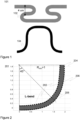
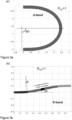
- FIG. 1 by way of example only, two different embodiments of the present invention are generally illustrated at 102 and 104. Bends such as 'U'-bends, 'S'-bends, 'L'-bends and practically any bend of a desired degree may be manufactured. Different basic bend shapes may be cleverly combined to establish more complex bends and (mirror/point) symmetry may be exploited to design the bends.
- the radius of curvature is to be gradually and continuously varied to produce the bend with more continuous and smoother transitions, while the bend size is minimized.
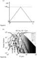
- Figures 6a , 6b, and 6c illustrate power coupling in the case of a prior art type 90 deg arc bend, matched 'L'-bend according to an embodiment of the present invention, and generic 'L'-bend according to another embodiment of the present invention, respectively, from the standpoint of bandwidth utilization.
- it is typically beneficial to analyze the spectral response of the bends for various reasons.
- the responses reflect the associated bends' tolerance to fabrication errors since one important design parameter is the ratio between the waveguide size and the wavelength, whereupon changing the wavelength is like changing the size and vice-versa.
- the matched bends were not precisely set to the transmission peak for 1.55 ⁇ m wavelength, but were optimized slightly off-resonance to ensure the highest operation bandwidth.
- the bend should be targeted to the smaller wavelengths of that range, and then optimized to cover the broadest possible range of longer wavelengths.
- a design that works at a given wavelength ⁇ 1 can be always rescaled to a different wavelength ⁇ 2 by simply rescaling waveguide width and bending radii by a factor ⁇ 2/ ⁇ 1 advantageously supplemented with some minor optimization to take into account effective refractive index dispersion of the given waveguide.
Landscapes
- Physics & Mathematics (AREA)
- General Physics & Mathematics (AREA)
- Optics & Photonics (AREA)
- Engineering & Computer Science (AREA)
- Microelectronics & Electronic Packaging (AREA)
- Optical Integrated Circuits (AREA)
Claims (9)
- Optischer Multimode-HIC-Wellenleiter (102, 104, 201, 301, 302) mit hohem Indexkontrast zum Transportieren elektromagnetischer Strahlung in dem optischen Wellenband, wobei der Wellenleiter ein Streifenwellenleiter ist,wobei der Wellenleiter einen leitenden Siliciumkernabschnitt (204) mit höherem Brechungsindex, und einen Siliciumdioxid-Ummantelungsabschnitt (206) mit im Wesentlichen niedrigerem Brechungsindex umfasst, der konfiguriert ist, um den lichtleitenden Kern in den Querrichtungen zu umgeben, um das Beschränken der sich ausbreitenden Strahlung innerhalb des Kerns zu erleichtern, wobei die Breite des Kernabschnitts 1-10 µm beträgt und die Dicke des Kernabschnitts 1-10 µm beträgt;wobei der Wellenleiter konfiguriert ist, um multiple optische Modi der sich ausbreitenden Strahlung zu unterstützen, wobei der relative Brechungsindexkontrast zwischen den Kern- und Ummantelungsabschnitten höher ist als 25%, und der Wellenleiter ein gebogenes Wellenleiterteilstück (202) einbezieht, das eine Biegekrümmung aufweist, die konfiguriert ist, um von einem Teilstückende allmählich und kontinuierlich in Richtung einer maximalen Krümmung des Teilstücks zuzunehmen.
- Wellenleiter nach Anspruch 1, wobei die Biegekrümmung von mindestens lokalen Minima an Teilstückenden in Richtung des Maximums zwischen den Enden zunimmt.
- Wellenleiter nach einem vorstehenden Anspruch, wobei die Teilstückenden im Wesentlichen gerade sind.
- Wellenleiter nach einem vorstehenden Anspruch, wobei das Teilstück zwei im Wesentlichen spiegelsymmetrische Unterteilstücke (202) enthält, wobei der Wellenleiter optional weiter ein anderes benachbartes, gebogenes Wellenleiterteilstück mit ähnlichen spiegelsymmetrischen Unterteilstücken umfasst, um eine vorgegebene doppelt symmetrische Struktur zu erstellen.
- Wellenleiter nach einem vorstehenden Anspruch, wobei sich der Punkt maximaler Krümmung (208) im Wesentlichen auf halbem Weg der Teilstücklänge befindet.
- Wellenleiter nach einem vorstehenden Anspruch, wobei die Krümmung mit der Biegelänge (401) zwischen dem Teilstückende und dem Punkt maximaler Krümmung im Wesentlichen linear variiert.
- Wellenleiter nach einem vorstehenden Anspruch, wobei das Teilstück oder Unterteilstück davon im Wesentlichen eine Form definiert, ausgewählt aus der Gruppe, bestehend aus: L-Biegung (201), U-Biegung (301) und einem Segment einer Spirale.
- Wellenleiter nach einem vorstehenden Anspruch, wobei der effektive oder minimale Krümmungsradius im Wesentlichen in der Größenordnung der Wellenleiterbreite liegt, vorzugsweise etwa das 20-fache der Wellenleiterbreite oder weniger, bevorzugter etwa das zehnfache der Breite oder weniger und besonders bevorzugt etwa das zweifache der Breite oder weniger beträgt.
- Vorrichtung, die den Wellenleiter nach einem vorstehenden Anspruch umfasst, wobei die Vorrichtung mindestens eine Entität definiert, ausgewählt aus der Gruppe, bestehend aus: elektronischer Vorrichtung, optoelektronischer Vorrichtung, photonischer Vorrichtung, optischem Schaltkreis, integriertem optischen Schaltkreis, Mikroringelement, Mikroringresonator, Interferometer, mehrstufigem kaskadierten Mach-Zehnder-Interferometer, Verzögerungsleitung, Reflektor, Multimode-Interferenzreflektor, Kommunikationsvorrichtung, SOI, Silicium-auf-Isolator-Vorrichtung, und Sensor.
Applications Claiming Priority (2)
| Application Number | Priority Date | Filing Date | Title |
|---|---|---|---|
| FI20126084A FI124843B (fi) | 2012-10-18 | 2012-10-18 | Taivutettu optinen aaltojohde |
| PCT/FI2013/050987 WO2014060648A1 (en) | 2012-10-18 | 2013-10-15 | Bent optical waveguide |
Publications (4)
| Publication Number | Publication Date |
|---|---|
| EP2909663A1 EP2909663A1 (de) | 2015-08-26 |
| EP2909663A4 EP2909663A4 (de) | 2016-07-20 |
| EP2909663C0 EP2909663C0 (de) | 2024-12-04 |
| EP2909663B1 true EP2909663B1 (de) | 2024-12-04 |
Family
ID=50487619
Family Applications (1)
| Application Number | Title | Priority Date | Filing Date |
|---|---|---|---|
| EP13846711.3A Active EP2909663B1 (de) | 2012-10-18 | 2013-10-15 | Gebogener optischer wellenleiter |
Country Status (7)
| Country | Link |
|---|---|
| US (1) | US9778417B2 (de) |
| EP (1) | EP2909663B1 (de) |
| JP (1) | JP6475626B2 (de) |
| CN (1) | CN104781708B (de) |
| CA (1) | CA2888597C (de) |
| FI (1) | FI124843B (de) |
| WO (1) | WO2014060648A1 (de) |
Families Citing this family (49)
| Publication number | Priority date | Publication date | Assignee | Title |
|---|---|---|---|---|
| GB2522252B (en) | 2014-01-20 | 2016-04-20 | Rockley Photonics Ltd | Tunable SOI laser |
| KR20150137780A (ko) * | 2014-05-30 | 2015-12-09 | 주식회사 포벨 | 꺽어진 광도파로를 가지는 외부 공진기형 레이저 |
| US9588296B2 (en) * | 2015-07-28 | 2017-03-07 | Lumentum Operations Llc | Semiconductor optical waveguide device |
| US9711930B2 (en) * | 2015-12-01 | 2017-07-18 | Seagate Technology Llc | Optical signal waveguide dispersion filter |
| JP6676964B2 (ja) * | 2015-12-25 | 2020-04-08 | 株式会社豊田中央研究所 | 光導波路 |
| US11699892B2 (en) | 2016-02-19 | 2023-07-11 | Rockley Photonics Limited | Discrete wavelength tunable laser |
| GB2547467A (en) | 2016-02-19 | 2017-08-23 | Rockley Photonics Ltd | Tunable laser |
| US10838146B2 (en) * | 2016-06-03 | 2020-11-17 | Rockley Photonics Limited | Single mode waveguide with an adiabatic bend |
| US11309619B2 (en) | 2016-09-23 | 2022-04-19 | Intel Corporation | Waveguide coupling systems and methods |
| US10566672B2 (en) | 2016-09-27 | 2020-02-18 | Intel Corporation | Waveguide connector with tapered slot launcher |
| US10256521B2 (en) | 2016-09-29 | 2019-04-09 | Intel Corporation | Waveguide connector with slot launcher |
| US11394094B2 (en) | 2016-09-30 | 2022-07-19 | Intel Corporation | Waveguide connector having a curved array of waveguides configured to connect a package to excitation elements |
| US10488589B2 (en) | 2017-02-08 | 2019-11-26 | Rockley Photonics Limited | T-shaped arrayed waveguide grating |
| JP7047256B2 (ja) * | 2017-03-29 | 2022-04-05 | 株式会社豊田中央研究所 | 光分配器および光アンテナ |
| US12368283B2 (en) | 2017-06-14 | 2025-07-22 | Rockley Photonics Limited | Broadband arbitrary wavelength multichannel laser source |
| US10811848B2 (en) | 2017-06-14 | 2020-10-20 | Rockley Photonics Limited | Broadband arbitrary wavelength multichannel laser source |
| WO2019016603A1 (en) | 2017-07-17 | 2019-01-24 | Rockley Photonics Limited | MULTI-PATH INTERFERENCE FILTER ATHERMALIZED |
| EP3673325B1 (de) * | 2017-08-22 | 2024-11-20 | Teknologian Tutkimuskeskus VTT OY | Integriertes faraday-drehgelenk |
| KR20190064964A (ko) * | 2017-12-01 | 2019-06-11 | 삼성전자주식회사 | 마이크로 스케일의 도파관 분광기 |
| FR3079037B1 (fr) * | 2018-03-15 | 2020-09-04 | St Microelectronics Crolles 2 Sas | Dispositif de terminaison de guide d'onde |
| GB2572641B (en) | 2018-04-06 | 2021-06-02 | Rockley Photonics Ltd | Optoelectronic device and array thereof |
| US10372014B1 (en) | 2018-11-15 | 2019-08-06 | Psiquantum, Corp. | Coupled resonator photon-pair sources |
| US10962782B2 (en) * | 2018-11-27 | 2021-03-30 | Microsoft Technology Licensing, Llc | Exit pupil expansion via curved waveguide |
| US11275210B1 (en) | 2018-12-07 | 2022-03-15 | PsiQuantum Corp. | Waveguide couplers for multi-mode waveguides |
| CN111338025A (zh) * | 2018-12-19 | 2020-06-26 | 中兴光电子技术有限公司 | 一种滤模装置和方法 |
| US11048042B2 (en) * | 2019-04-01 | 2021-06-29 | Lumentum Operations Llc | Curved waveguide configuration to suppress mode conversion |
| CN110082857B (zh) * | 2019-04-28 | 2020-06-16 | 浙江大学 | 一种基于金属纳米颗粒耦合结构的弯曲微纳光波导 |
| US11391890B1 (en) | 2019-05-15 | 2022-07-19 | PsiQuantum Corp. | Multi-mode spiral delay device |
| CN110221384B (zh) * | 2019-06-17 | 2020-07-10 | 华中科技大学 | 一种硅基超材料多模弯曲波导及其制备方法 |
| EP3997493B1 (de) * | 2019-07-09 | 2026-04-29 | Hyperlight Corporation | Verlustarme wellenleiterstrukturen, insbesondere modulatoren |
| US11474384B2 (en) | 2020-04-02 | 2022-10-18 | HyperLight Corporation | Velocity matched electro-optic devices |
| JP2021067898A (ja) * | 2019-10-28 | 2021-04-30 | アダマンド並木精密宝石株式会社 | 光伝搬装置 |
| US11333682B2 (en) | 2020-03-13 | 2022-05-17 | Huawei Technologies Canada Co., Ltd. | Silicon probe for millimeter-wave and terahertz measurement and characterization |
| CN111338028A (zh) * | 2020-03-25 | 2020-06-26 | 南通赛勒光电科技有限公司 | 一种新型的硅基波分复用器结构 |
| US12032211B1 (en) | 2020-10-19 | 2024-07-09 | HyperLight Corporation | Large mode coupler |
| WO2022184869A1 (en) | 2021-03-05 | 2022-09-09 | Rockley Photonics Limited | Higher order mode filter |
| WO2022184868A1 (en) | 2021-03-05 | 2022-09-09 | Rockley Photonics Limited | Waveguide facet interface |
| CN113050220A (zh) * | 2021-03-15 | 2021-06-29 | 中国科学院微电子研究所 | 一种渐变弯曲波导器件 |
| US11740418B2 (en) | 2021-03-23 | 2023-08-29 | Globalfoundries U.S. Inc. | Barrier structure with passage for waveguide in photonic integrated circuit |
| WO2022263612A1 (en) * | 2021-06-16 | 2022-12-22 | Rockley Photonics Limited | Optoelectronic device and array thereof |
| WO2023272690A1 (zh) * | 2021-07-01 | 2023-01-05 | 深圳市速腾聚创科技有限公司 | 脊形波导、微环谐振器、可调光延迟线及芯片 |
| JP2023040871A (ja) * | 2021-09-10 | 2023-03-23 | 富士通オプティカルコンポーネンツ株式会社 | 光導波路素子および光集積回路 |
| US12449683B1 (en) | 2021-11-04 | 2025-10-21 | HyperLight Corporation | Dual height functional components in lithium niobate optical devices |
| US12321051B1 (en) | 2021-11-05 | 2025-06-03 | HyperLight Corporation | Mode converter |
| CN114005923B (zh) * | 2021-11-19 | 2025-02-14 | 长春理工大学 | 前端双窗口双光束小夹角输出超辐射发光二极管 |
| CN115793145B (zh) * | 2022-12-16 | 2025-07-04 | 湖南师范大学 | 一种微流控波导型可变光衰减器 |
| CN116880011B (zh) * | 2023-07-18 | 2025-03-21 | 浙江大学 | 一种基于高阶模转换的零色散低损耗延迟线 |
| CN119620291B (zh) * | 2024-11-29 | 2025-12-05 | 中国航空工业集团公司北京长城计量测试技术研究所 | 一种低重频的螺旋微腔结构及设计方法 |
| CN120010057A (zh) * | 2025-03-13 | 2025-05-16 | 浙江大学 | 一种基于自由形式曲线设计的高q值微环谐振器及滤波器 |
Family Cites Families (20)
| Publication number | Priority date | Publication date | Assignee | Title |
|---|---|---|---|---|
| EP0645649A3 (de) * | 1993-09-23 | 1995-05-17 | Siemens Ag | Gekrümmter streifenförmiger integriert optischer Wellenleiter. |
| JPH1164654A (ja) * | 1997-08-15 | 1999-03-05 | Nippon Telegr & Teleph Corp <Ntt> | 光導波路 |
| JPH11248949A (ja) * | 1998-02-27 | 1999-09-17 | Hitachi Cable Ltd | 光波長合分波器 |
| JP2004512551A (ja) * | 2000-10-13 | 2004-04-22 | マサチューセッツ インスティテュート オブ テクノロジー | トレンチ構造体を有する光導波管 |
| US6801698B2 (en) * | 2001-04-12 | 2004-10-05 | Omniguide Communications | High index-contrast fiber waveguides and applications |
| US6731841B1 (en) * | 2002-05-24 | 2004-05-04 | Alliance Fiber Optic Products, Inc. | Folded waveguide optical devices |
| JP3903940B2 (ja) * | 2003-03-31 | 2007-04-11 | Jsr株式会社 | 光導波路チップ及びそれを含む光学部品の製造方法 |
| EP1464997A1 (de) * | 2003-04-04 | 2004-10-06 | ThreeFive Photonics B.V. | Integrierte optische Vorrichtung mit einem gekrümmten Wellenleiter |
| CA2534970A1 (en) * | 2003-08-04 | 2005-02-17 | Pirelli & C. S.P.A. | Integrated optical waveguide structure with low coupling losses to an external optical field |
| JP4214862B2 (ja) * | 2003-08-21 | 2009-01-28 | 富士ゼロックス株式会社 | ピッチ変換導波路アレイ |
| JP4202212B2 (ja) * | 2003-08-26 | 2008-12-24 | 日本電信電話株式会社 | 光導波路 |
| WO2006081633A1 (en) * | 2005-02-07 | 2006-08-10 | Rpo Pty Limited | Waveguide design incorporating reflective optics |
| US7248772B2 (en) * | 2005-07-26 | 2007-07-24 | Fuji Xerox Co., Ltd. | Flexible optical waveguide |
| JP2007072433A (ja) | 2005-08-11 | 2007-03-22 | Ricoh Co Ltd | 光集積素子及び光制御素子 |
| JP2007052328A (ja) | 2005-08-19 | 2007-03-01 | Ricoh Co Ltd | 複合光導波路 |
| US8300996B2 (en) * | 2010-07-30 | 2012-10-30 | Hewlett-Packard Development Company, L.P. | Optical bus for optical signal broadcasting |
| US8737777B2 (en) * | 2012-01-03 | 2014-05-27 | Xyratex Technology Limited | Optical waveguide and a method for making an optical waveguide |
| US9044907B2 (en) * | 2012-01-20 | 2015-06-02 | Xyratex Technology Limited—A Seagate Company | Method of, and apparatus for, making an optical waveguide |
| US8903205B2 (en) * | 2012-02-23 | 2014-12-02 | Karlsruhe Institute of Technology (KIT) | Three-dimensional freeform waveguides for chip-chip connections |
| JP5702756B2 (ja) | 2012-08-22 | 2015-04-15 | 株式会社フジクラ | 光導波路素子 |
-
2012
- 2012-10-18 FI FI20126084A patent/FI124843B/fi active IP Right Grant
-
2013
- 2013-10-15 CA CA2888597A patent/CA2888597C/en active Active
- 2013-10-15 EP EP13846711.3A patent/EP2909663B1/de active Active
- 2013-10-15 JP JP2015537316A patent/JP6475626B2/ja active Active
- 2013-10-15 US US14/436,093 patent/US9778417B2/en active Active
- 2013-10-15 CN CN201380054234.8A patent/CN104781708B/zh active Active
- 2013-10-15 WO PCT/FI2013/050987 patent/WO2014060648A1/en not_active Ceased
Non-Patent Citations (5)
| Title |
|---|
| ANDREA MELLONI ET AL: "Experimental confirmation of matched bends", OPTICS LETTERS, vol. 29, no. 5, 1 March 2004 (2004-03-01), pages 465 - 467, XP055368310, ISSN: 0146-9592, DOI: 10.1364/OL.29.000465 * |
| CH KOOS ET AL: "Ideal Trajectory for Ultracompact Low-Loss Waveguide Bends", PROCEEDINGS / ECOC 2006, 32ND EUROPEAN CONFERENCE ON OPTICAL COMMUNICATION : 24 - 28 SEPTEMBER 2006, CANNES, FRANCE, SEE, PARIS, FRANCE, 24 September 2006 (2006-09-24), pages 1 - 2, XP031437148, ISBN: 978-2-912328-39-7 * |
| H KELDERMAN ET AL: "Bends in polymeric multimode waveguides", 1 January 2007 (2007-01-01), XP055368318, Retrieved from the Internet <URL:http://doc.utwente.nl/64377/1/Kelderman_H._-ECIO_-_27-28-4-2007_Copenhagen_Denmark.pdf> * |
| MEE-KOY CHIN ET AL: "High-index-contrast waveguides and devices", APPLIED OPTICS, vol. 44, no. 15, 20 May 2005 (2005-05-20), WASHINGTON, DC; US, pages 3077, XP055368314, ISSN: 0003-6935, DOI: 10.1364/AO.44.003077 * |
| RICHARD PITWON ET AL: "Polymer optical waveguides with reduced in-plane bend loss for electro-optical PCBs", SPIE - INTERNATIONAL SOCIETY FOR OPTICAL ENGINEERING. PROCEEDINGS, vol. 8264, 9 February 2012 (2012-02-09), US, pages 82640Z, XP055368307, ISSN: 0277-786X, ISBN: 978-1-5106-0753-8, DOI: 10.1117/12.919817 * |
Also Published As
| Publication number | Publication date |
|---|---|
| CN104781708B (zh) | 2019-05-17 |
| US9778417B2 (en) | 2017-10-03 |
| EP2909663A1 (de) | 2015-08-26 |
| EP2909663C0 (de) | 2024-12-04 |
| CN104781708A (zh) | 2015-07-15 |
| US20150260916A1 (en) | 2015-09-17 |
| WO2014060648A1 (en) | 2014-04-24 |
| CA2888597C (en) | 2020-06-09 |
| FI124843B (fi) | 2015-02-13 |
| FI20126084L (fi) | 2014-04-19 |
| JP2015532470A (ja) | 2015-11-09 |
| EP2909663A4 (de) | 2016-07-20 |
| CA2888597A1 (en) | 2014-04-24 |
| JP6475626B2 (ja) | 2019-02-27 |
Similar Documents
| Publication | Publication Date | Title |
|---|---|---|
| US9778417B2 (en) | Bent optical waveguide | |
| US10663663B2 (en) | Spot-size converter for optical mode conversion and coupling between two waveguides | |
| Cherchi et al. | Dramatic size reduction of waveguide bends on a micron-scale silicon photonic platform | |
| US7680371B2 (en) | Interface device for performing mode transformation in optical waveguides | |
| JP6365855B2 (ja) | 一連のベンドを備える導波路型偏光子のための装置および方法 | |
| US9703047B2 (en) | Spot-size converter for optical mode conversion and coupling between two waveguides | |
| US9279939B2 (en) | Spot-size converter | |
| US20180224605A1 (en) | Spot-size converter for optical mode conversion and coupling between two waveguides | |
| US9221074B2 (en) | Stress-tuned planar lightwave circuit and method therefor | |
| US20080193079A1 (en) | Interface Device For Performing Mode Transformation in Optical Waveguides | |
| US20160306117A1 (en) | Tapered polymer waveguide | |
| US20080044126A1 (en) | Integrated Optical Waveguide Structure with Low Coupling Losses to an External Optical Field | |
| US20040202429A1 (en) | Planar optical component for coupling light to a high index waveguide, and method of its manufacture | |
| WO2018051370A1 (en) | Broadband wavelength filter device using sidewall grating for filtering optical signals | |
| CN112470050A (zh) | 具有空间调制折射率区域的光学波导 | |
| JP6003069B2 (ja) | グレーティング素子及び光素子 | |
| EP3227750B1 (de) | Belastungsabgestimmte planare lichtwellenschaltung und verfahren dafür | |
| US20110317960A1 (en) | Direct coupling of optical slot waveguide to another optical waveguide | |
| Cheben et al. | Subwavelength index engineered waveguides and devices | |
| Navalakhe et al. | Design of low-loss compact 90° bend optical waveguide for photonic circuit applications in SOI platform | |
| Cherchi et al. | New silicon photonics integration platform enabled by novel micron-scale bends | |
| Timotijevic et al. | Optical filters in silicon-on-insulator: design considerations for devices based upon strip and rib waveguides | |
| Zhu et al. | Integrated plasmonic waveguide at the mid-infrared | |
| Zhou et al. | High-performance and compact polarization-independent grating coupler | |
| Aalto et al. | Bend-size reduction on the SOI rib waveguide platform |
Legal Events
| Date | Code | Title | Description |
|---|---|---|---|
| PUAI | Public reference made under article 153(3) epc to a published international application that has entered the european phase |
Free format text: ORIGINAL CODE: 0009012 |
|
| 17P | Request for examination filed |
Effective date: 20150515 |
|
| AK | Designated contracting states |
Kind code of ref document: A1 Designated state(s): AL AT BE BG CH CY CZ DE DK EE ES FI FR GB GR HR HU IE IS IT LI LT LU LV MC MK MT NL NO PL PT RO RS SE SI SK SM TR |
|
| AX | Request for extension of the european patent |
Extension state: BA ME |
|
| DAX | Request for extension of the european patent (deleted) | ||
| RA4 | Supplementary search report drawn up and despatched (corrected) |
Effective date: 20160622 |
|
| RIC1 | Information provided on ipc code assigned before grant |
Ipc: G02B 6/125 20060101AFI20160615BHEP Ipc: G02B 6/02 20060101ALI20160615BHEP Ipc: G02B 6/26 20060101ALI20160615BHEP Ipc: G02B 6/122 20060101ALI20160615BHEP |
|
| STAA | Information on the status of an ep patent application or granted ep patent |
Free format text: STATUS: EXAMINATION IS IN PROGRESS |
|
| 17Q | First examination report despatched |
Effective date: 20170508 |
|
| GRAP | Despatch of communication of intention to grant a patent |
Free format text: ORIGINAL CODE: EPIDOSNIGR1 |
|
| STAA | Information on the status of an ep patent application or granted ep patent |
Free format text: STATUS: GRANT OF PATENT IS INTENDED |
|
| INTG | Intention to grant announced |
Effective date: 20240621 |
|
| GRAS | Grant fee paid |
Free format text: ORIGINAL CODE: EPIDOSNIGR3 |
|
| RAP3 | Party data changed (applicant data changed or rights of an application transferred) |
Owner name: TEKNOLOGIAN TUTKIMUSKESKUS VTT OY |
|
| GRAA | (expected) grant |
Free format text: ORIGINAL CODE: 0009210 |
|
| STAA | Information on the status of an ep patent application or granted ep patent |
Free format text: STATUS: THE PATENT HAS BEEN GRANTED |
|
| AK | Designated contracting states |
Kind code of ref document: B1 Designated state(s): AL AT BE BG CH CY CZ DE DK EE ES FI FR GB GR HR HU IE IS IT LI LT LU LV MC MK MT NL NO PL PT RO RS SE SI SK SM TR |
|
| REG | Reference to a national code |
Ref country code: GB Ref legal event code: FG4D |
|
| REG | Reference to a national code |
Ref country code: CH Ref legal event code: EP |
|
| REG | Reference to a national code |
Ref country code: DE Ref legal event code: R096 Ref document number: 602013086340 Country of ref document: DE |
|
| REG | Reference to a national code |
Ref country code: IE Ref legal event code: FG4D |
|
| U01 | Request for unitary effect filed |
Effective date: 20241205 |
|
| U07 | Unitary effect registered |
Designated state(s): AT BE BG DE DK EE FI FR IT LT LU LV MT NL PT RO SE SI Effective date: 20241216 |
|
| PG25 | Lapsed in a contracting state [announced via postgrant information from national office to epo] |
Ref country code: HR Free format text: LAPSE BECAUSE OF FAILURE TO SUBMIT A TRANSLATION OF THE DESCRIPTION OR TO PAY THE FEE WITHIN THE PRESCRIBED TIME-LIMIT Effective date: 20241204 |
|
| PG25 | Lapsed in a contracting state [announced via postgrant information from national office to epo] |
Ref country code: ES Free format text: LAPSE BECAUSE OF FAILURE TO SUBMIT A TRANSLATION OF THE DESCRIPTION OR TO PAY THE FEE WITHIN THE PRESCRIBED TIME-LIMIT Effective date: 20241204 |
|
| PG25 | Lapsed in a contracting state [announced via postgrant information from national office to epo] |
Ref country code: NO Free format text: LAPSE BECAUSE OF FAILURE TO SUBMIT A TRANSLATION OF THE DESCRIPTION OR TO PAY THE FEE WITHIN THE PRESCRIBED TIME-LIMIT Effective date: 20250304 |
|
| PG25 | Lapsed in a contracting state [announced via postgrant information from national office to epo] |
Ref country code: GR Free format text: LAPSE BECAUSE OF FAILURE TO SUBMIT A TRANSLATION OF THE DESCRIPTION OR TO PAY THE FEE WITHIN THE PRESCRIBED TIME-LIMIT Effective date: 20250305 |
|
| PG25 | Lapsed in a contracting state [announced via postgrant information from national office to epo] |
Ref country code: RS Free format text: LAPSE BECAUSE OF FAILURE TO SUBMIT A TRANSLATION OF THE DESCRIPTION OR TO PAY THE FEE WITHIN THE PRESCRIBED TIME-LIMIT Effective date: 20250304 |
|
| PG25 | Lapsed in a contracting state [announced via postgrant information from national office to epo] |
Ref country code: SM Free format text: LAPSE BECAUSE OF FAILURE TO SUBMIT A TRANSLATION OF THE DESCRIPTION OR TO PAY THE FEE WITHIN THE PRESCRIBED TIME-LIMIT Effective date: 20241204 |
|
| PG25 | Lapsed in a contracting state [announced via postgrant information from national office to epo] |
Ref country code: PL Free format text: LAPSE BECAUSE OF FAILURE TO SUBMIT A TRANSLATION OF THE DESCRIPTION OR TO PAY THE FEE WITHIN THE PRESCRIBED TIME-LIMIT Effective date: 20241204 |
|
| PG25 | Lapsed in a contracting state [announced via postgrant information from national office to epo] |
Ref country code: IS Free format text: LAPSE BECAUSE OF FAILURE TO SUBMIT A TRANSLATION OF THE DESCRIPTION OR TO PAY THE FEE WITHIN THE PRESCRIBED TIME-LIMIT Effective date: 20250404 |
|
| PG25 | Lapsed in a contracting state [announced via postgrant information from national office to epo] |
Ref country code: SK Free format text: LAPSE BECAUSE OF FAILURE TO SUBMIT A TRANSLATION OF THE DESCRIPTION OR TO PAY THE FEE WITHIN THE PRESCRIBED TIME-LIMIT Effective date: 20241204 |
|
| PG25 | Lapsed in a contracting state [announced via postgrant information from national office to epo] |
Ref country code: CZ Free format text: LAPSE BECAUSE OF FAILURE TO SUBMIT A TRANSLATION OF THE DESCRIPTION OR TO PAY THE FEE WITHIN THE PRESCRIBED TIME-LIMIT Effective date: 20241204 |
|
| PLBE | No opposition filed within time limit |
Free format text: ORIGINAL CODE: 0009261 |
|
| STAA | Information on the status of an ep patent application or granted ep patent |
Free format text: STATUS: NO OPPOSITION FILED WITHIN TIME LIMIT |
|
| 26N | No opposition filed |
Effective date: 20250905 |
|
| U20 | Renewal fee for the european patent with unitary effect paid |
Year of fee payment: 13 Effective date: 20251028 |
|
| PGFP | Annual fee paid to national office [announced via postgrant information from national office to epo] |
Ref country code: GB Payment date: 20251022 Year of fee payment: 13 |