EP2911187A1 - Ätzverfahren - Google Patents
Ätzverfahren Download PDFInfo
- Publication number
- EP2911187A1 EP2911187A1 EP15155980.4A EP15155980A EP2911187A1 EP 2911187 A1 EP2911187 A1 EP 2911187A1 EP 15155980 A EP15155980 A EP 15155980A EP 2911187 A1 EP2911187 A1 EP 2911187A1
- Authority
- EP
- European Patent Office
- Prior art keywords
- region
- etching
- gas
- fluorocarbon
- plasma
- Prior art date
- Legal status (The legal status is an assumption and is not a legal conclusion. Google has not performed a legal analysis and makes no representation as to the accuracy of the status listed.)
- Withdrawn
Links
Images



Classifications
-
- H—ELECTRICITY
- H10—SEMICONDUCTOR DEVICES; ELECTRIC SOLID-STATE DEVICES NOT OTHERWISE PROVIDED FOR
- H10P—GENERIC PROCESSES OR APPARATUS FOR THE MANUFACTURE OR TREATMENT OF DEVICES COVERED BY CLASS H10
- H10P50/00—Etching of wafers, substrates or parts of devices
- H10P50/20—Dry etching; Plasma etching; Reactive-ion etching
- H10P50/28—Dry etching; Plasma etching; Reactive-ion etching of insulating materials
- H10P50/282—Dry etching; Plasma etching; Reactive-ion etching of insulating materials of inorganic materials
- H10P50/283—Dry etching; Plasma etching; Reactive-ion etching of insulating materials of inorganic materials by chemical means
-
- H—ELECTRICITY
- H01—ELECTRIC ELEMENTS
- H01J—ELECTRIC DISCHARGE TUBES OR DISCHARGE LAMPS
- H01J37/00—Discharge tubes with provision for introducing objects or material to be exposed to the discharge, e.g. for the purpose of examination or processing thereof
- H01J37/32—Gas-filled discharge tubes
- H01J37/32009—Arrangements for generation of plasma specially adapted for examination or treatment of objects, e.g. plasma sources
- H01J37/32082—Radio frequency generated discharge
- H01J37/32091—Radio frequency generated discharge the radio frequency energy being capacitively coupled to the plasma
-
- H—ELECTRICITY
- H10—SEMICONDUCTOR DEVICES; ELECTRIC SOLID-STATE DEVICES NOT OTHERWISE PROVIDED FOR
- H10P—GENERIC PROCESSES OR APPARATUS FOR THE MANUFACTURE OR TREATMENT OF DEVICES COVERED BY CLASS H10
- H10P14/00—Formation of materials, e.g. in the shape of layers or pillars
- H10P14/60—Formation of materials, e.g. in the shape of layers or pillars of insulating materials
- H10P14/69—Inorganic materials
- H10P14/692—Inorganic materials composed of oxides, glassy oxides or oxide-based glasses
- H10P14/6921—Inorganic materials composed of oxides, glassy oxides or oxide-based glasses containing silicon
- H10P14/69215—Inorganic materials composed of oxides, glassy oxides or oxide-based glasses containing silicon the material being a silicon oxide, e.g. SiO2
-
- H—ELECTRICITY
- H10—SEMICONDUCTOR DEVICES; ELECTRIC SOLID-STATE DEVICES NOT OTHERWISE PROVIDED FOR
- H10P—GENERIC PROCESSES OR APPARATUS FOR THE MANUFACTURE OR TREATMENT OF DEVICES COVERED BY CLASS H10
- H10P14/00—Formation of materials, e.g. in the shape of layers or pillars
- H10P14/60—Formation of materials, e.g. in the shape of layers or pillars of insulating materials
- H10P14/69—Inorganic materials
- H10P14/694—Inorganic materials composed of nitrides
- H10P14/6943—Inorganic materials composed of nitrides containing silicon
- H10P14/69433—Inorganic materials composed of nitrides containing silicon the material being a silicon nitride not containing oxygen, e.g. SixNy or SixByNz
-
- H—ELECTRICITY
- H10—SEMICONDUCTOR DEVICES; ELECTRIC SOLID-STATE DEVICES NOT OTHERWISE PROVIDED FOR
- H10P—GENERIC PROCESSES OR APPARATUS FOR THE MANUFACTURE OR TREATMENT OF DEVICES COVERED BY CLASS H10
- H10P50/00—Etching of wafers, substrates or parts of devices
- H10P50/20—Dry etching; Plasma etching; Reactive-ion etching
- H10P50/28—Dry etching; Plasma etching; Reactive-ion etching of insulating materials
-
- H—ELECTRICITY
- H10—SEMICONDUCTOR DEVICES; ELECTRIC SOLID-STATE DEVICES NOT OTHERWISE PROVIDED FOR
- H10P—GENERIC PROCESSES OR APPARATUS FOR THE MANUFACTURE OR TREATMENT OF DEVICES COVERED BY CLASS H10
- H10P95/00—Generic processes or apparatus for manufacture or treatments not covered by the other groups of this subclass
- H10P95/06—Planarisation of inorganic insulating materials
- H10P95/062—Planarisation of inorganic insulating materials involving a dielectric removal step
- H10P95/064—Planarisation of inorganic insulating materials involving a dielectric removal step the removal being chemical etching
-
- H—ELECTRICITY
- H10—SEMICONDUCTOR DEVICES; ELECTRIC SOLID-STATE DEVICES NOT OTHERWISE PROVIDED FOR
- H10W—GENERIC PACKAGES, INTERCONNECTIONS, CONNECTORS OR OTHER CONSTRUCTIONAL DETAILS OF DEVICES COVERED BY CLASS H10
- H10W20/00—Interconnections in chips, wafers or substrates
- H10W20/01—Manufacture or treatment
- H10W20/031—Manufacture or treatment of conductive parts of the interconnections
- H10W20/069—Manufacture or treatment of conductive parts of the interconnections by forming self-aligned vias or self-aligned contact plugs
-
- H—ELECTRICITY
- H10—SEMICONDUCTOR DEVICES; ELECTRIC SOLID-STATE DEVICES NOT OTHERWISE PROVIDED FOR
- H10W—GENERIC PACKAGES, INTERCONNECTIONS, CONNECTORS OR OTHER CONSTRUCTIONAL DETAILS OF DEVICES COVERED BY CLASS H10
- H10W20/00—Interconnections in chips, wafers or substrates
- H10W20/01—Manufacture or treatment
- H10W20/071—Manufacture or treatment of dielectric parts thereof
- H10W20/081—Manufacture or treatment of dielectric parts thereof by forming openings in the dielectric parts
Definitions
- the embodiments described herein pertain generally to an etching method.
- etching the silicon oxide film In manufacturing electronic devices, by performing an etching process on a silicon oxide film serving as an insulating layer, holes or trenches are formed therein.
- a target object In etching the silicon oxide film, generally, a target object is exposed to plasma of a fluorocarbon gas, so that the silicon oxide film is etched as described in Patent Document 1.
- the silicon oxide film is etched by active species of fluorine. Further, in the etching process, fluorocarbon is deposited on the silicon oxide film to form a deposit thereon.
- Patent Document 1 Specification of U.S. Patent No. 7708859
- a film thickness of the deposit gradually increases.
- the increase in the film thickness of the deposit suppresses active species capable of etching the silicon oxide film from reaching the silicon oxide film.
- the etching process on the silicon oxide film is stopped on the way. Accordingly, an etching rate of the silicon oxide film is decreased.
- an etching method of etching a region formed of silicon oxide includes an exposing process of exposing a target object including the region to plasma of a processing gas containing a fluorocarbon gas, etching the region, and forming a deposit containing fluorocarbon on the region (hereinafter, referred as "process (a)”); and an etching process of etching the region with a radical of the fluorocarbon contained in the deposit (hereinafter, referred as "process (b)").
- process (a) a processing gas containing a fluorocarbon gas
- process (b) an etching process of etching the region with a radical of the fluorocarbon contained in the deposit
- the region formed of the silicon oxide is etched with the plasma of the fluorocarbon gas generated in the process (a), and the deposit is formed on the region. Then, in the process (b), the region is further etched with the radical of the fluorocarbon included in the deposit. Further, in the process (b), the amount of the deposit is decreased. Therefore, by further performing the process (a), the region is further etched.
- the process (a) and the process (b) it is possible to suppress etching of the region, i.e., a silicon oxide film, from being stopped. As a result, it is possible to continuously perform the etching of the silicon oxide film.
- the target object may be exposed to plasma of a rare gas. That is, the deposit may be exposed to the plasma of the rare gas.
- the radical of the fluorocarbon in the deposit etches the region. Further, in the process (b) of the example embodiment, the fluorocarbon gas may not be supplied.
- the target object may further include a region formed of silicon nitride.
- a region formed of silicon nitride it is possible to etch the region formed of the silicon oxide with respect to the region formed of the silicon nitride with a high selectivity.
- the process (a) and the process (b) may be performed in a capacitively coupled plasma processing apparatus including an upper electrode.
- the upper electrode may have an electrode plate made of silicon, and the upper electrode may be connected to a power supply configured to apply a voltage for attracting positive ions to the electrode plate.
- the voltage may be applied to the upper electrode in at least one of the process (a) and the process (b).
- silicon since positive ions collide with the electrode plate, silicon is released from the electrode plate. The released silicon is bonded to the active species of fluorine within the plasma processing apparatus to reduce the amount of the active species of the fluorine. As a result, it is possible to suppress the region formed of the silicon nitride from being etched and also possible to etch the region formed of the silicon oxide with a higher selectivity.
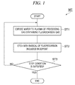
- FIG. 1 is a flow chart illustrating an etching method in accordance with an example embodiment.
- a method MT illustrated in FIG. 1 is a method of etching a region formed of silicon oxide.
- the method may be performed on a target object (hereinafter, referred to as "wafer W") including a first region formed of silicon oxide and a second region formed of silicon nitride.
- wafer W target object
- FIG. 2 is a diagram illustrating the plasma processing apparatus in accordance with the example embodiment.
- a plasma processing apparatus 10 illustrated in FIG. 2 is configured as a capacitively coupled plasma etching apparatus and includes a substantially cylindrical processing chamber 12.
- An inner wall surface of the processing chamber 12 is formed of, for example, anodically oxidized aluminum.
- the processing chamber 12 is frame-grounded.
- a substantially cylindrical supporting member 14 is provided on a bottom portion of the processing chamber 12.
- the supporting member 14 is formed of, for example, an insulating material.
- the supporting member 14 is vertically extended from the bottom portion within the processing chamber 12.
- a mounting table PD is provided within the processing chamber 12. The mounting table PD is supported on the supporting member 14.
- the mounting table PD is configured to hold the wafer W thereon.
- the mounting table PD includes a lower electrode LE and an electrostatic chuck ESC.
- the lower electrode LE includes a first plate 18a and a second plate 18b.
- the first plate 18a and the second plate 18b are formed of a metal such as aluminum, and each of the first plate 18a and the second plate 18b has a substantially disc shape.
- the second plate 18b is provided on the first plate 18a and electrically connected with the first plate 18a.
- the electrostatic chuck ESC is provided on the second plate 18b.
- the electrostatic chuck ESC has a structure in which an electrode as a conductive film is arranged between a pair of insulating layers or insulating sheets.
- the electrode of the electrostatic chuck ESC is electrically connected to a DC power supply 22 via a switch 23.
- the electrostatic chuck ESC is configured to attract the wafer W by an electrostatic force such as a Coulomb force generated by a DC voltage from the DC power supply 22.
- the electrostatic chuck ESC can hold the wafer W.
- a focus ring FR is arranged to surround an edge of the wafer W and the electrostatic chuck ESC.
- the focus ring FR is provided to improve the etching uniformity.
- the focus ring FR is formed of a material appropriately selected depending on a material of an etching target film, and may be formed of, for example, quartz.
- a coolant path 24 is formed within the second plate 18b.
- the coolant path 24 serves as a temperature control device.
- a chiller unit provided outside the processing chamber 12 is configured to supply a coolant into the coolant path 24 through a line 26a.
- the coolant supplied into the coolant path 24 is returned back to the chiller unit through a line 26b.
- the coolant is supplied to be circulated through the coolant path 24.
- a gas supply line 28 is provided in the plasma processing apparatus 10.
- the gas supply line 28 is configured to supply a heat transfer gas, for example, a He gas, from a heat transfer gas supply unit into a gap between an upper surface of the electrostatic chuck ESC and a rear surface of the wafer W.
- a heat transfer gas for example, a He gas
- the plasma processing apparatus 10 includes an upper electrode 30.
- the upper electrode 30 is arranged above the mounting table PD to face the mounting table PD.
- the lower electrode LE and the upper electrode 30 are provided to be substantially parallel to each other. Between the upper electrode 30 and the lower electrode LE, there is formed a processing space S in which a plasma process is performed on the wafer W.
- the upper electrode 30 is supported at an upper portion of the processing chamber 12 via an insulating shield member 32.
- the upper electrode 30 may be configured such that a vertical distance between the upper electrode 30 and an upper surface of the mounting table PD, i.e., a mounting surface of the wafer can be varied.
- the upper electrode 30 may include an electrode plate 34 and an electrode supporting body 36.
- the electrode plate 34 faces the processing space S, and multiple gas discharge holes 34a are formed through the electrode plate 34.
- the electrode plate 34 is formed of silicon in the example embodiment.
- the electrode supporting body 36 detachably supports the electrode plate 34 and may be formed of a conductive material such as aluminum.
- the electrode supporting body 36 may have a water-cooling structure.
- a gas diffusion space 36a is formed within the electrode supporting body 36. From the gas diffusion space 36a, multiple gas through holes 36b communicating with the gas discharge holes 34a are extended downwards. Further, a gas inlet opening 36c for introducing a processing gas into the gas diffusion space 36a is formed at the electrode supporting body 36 and connected to a gas supply line 38.
- the gas supply line 38 is connected to a gas source group 40 via a valve group 42 and a flow rate controller group 44.
- the gas source group 40 includes multiple gas sources such as a source of a fluorocarbon gas, a source of a rare gas, and a source of an oxygen (O 2 ) gas.
- the fluorocarbon gas may include at least one of, for example, a C 4 F 6 gas and a C 4 F 8 gas.
- the rare gas may include at least one of various rare gases such as an Ar gas and a He gas.
- the valve group 42 includes multiple valves, and the flow rate controller group 44 includes multiple flow rate controllers such as mass flow controllers.
- Each of the multiple gas sources belonging to the gas source group 40 is connected to the gas supply line 38 via a corresponding valve belonging to the valve group 42 and a corresponding flow rate controller belonging to the flow rate controller group 44.
- a deposition shield 46 is detachably provided along an inner wall of the processing chamber 12.
- the deposition shield 46 is also provided at an outer periphery of the supporting member 14.
- the deposition shield 46 is configured to suppress the etching by-products (deposits) from being deposited on the processing chamber 12 and may be formed by coating an aluminum member with ceramics such as Y 2 O 3 .
- a gas exhaust plate 48 is provided at a side of the bottom portion of the processing chamber 12 and between the supporting member 14 and a sidewall of the processing chamber 12.
- the gas exhaust plate 48 may be formed by coating an aluminum member with ceramics such as Y 2 O 3 .
- a gas exhaust opening 12e is formed under the gas exhaust plate 48 and at the processing chamber 12.
- the gas exhaust opening 12e is connected to a gas exhaust device 50 via a gas exhaust line 52.
- the gas exhaust device 50 includes a vacuum pump such as a turbo molecular pump and is configured to depressurize a space within the processing chamber 12 to a desired vacuum level.
- a loading/unloading opening 12g for the wafer W is formed at the sidewall of the processing chamber 12, and is opened and closed by a gate valve 54.
- the plasma processing apparatus 10 further includes a first high frequency power supply 62 and a second high frequency power supply 64.
- the first high frequency power supply 62 is configured to supply a first high frequency power having a frequency of 27 MHz to 100 MHz, for example, 40 MHz for plasma generation.
- the first high frequency power supply 62 is connected to the lower electrode LE via a matching unit 66.
- the matching unit 66 is configured to match output impedance of the first high frequency power supply 62 with input impedance on a load side (on a side of the lower electrode LE).
- the second high frequency power supply 64 is configured to supply a high frequency power, i.e., a high frequency bias power, having a frequency of 400 kHz to 13.56 MHz, for example, 13 MHz for ion attraction into the wafer W.
- the second high frequency power supply 64 is connected to the lower electrode LE via a matching unit 68.
- the matching unit 68 is configured to match output impedance of the second high frequency power supply 64 with input impedance on the load side (on a side of the lower electrode LE).
- the plasma processing apparatus 10 further includes a power supply 70.
- the power supply 70 is connected to the upper electrode 30.
- the power supply 70 is configured to apply, to the upper electrode 30, a voltage for attracting positive ions present within the processing space S into the electrode plate 34.
- the power supply 70 is a DC power supply that generates a negative DC voltage.
- the power supply 70 may be an AC power supply that generates an AC voltage having a relatively low frequency.
- the voltage applied from the power supply 70 to the upper electrode may be -150 V or less. That is, the voltage applied from the power supply 70 to the upper electrode 30 may be a negative voltage having an absolute value of 150 or more.
- the positive ions within the processing space S collide with the electrode plate 34.
- secondary electrons and/or silicon are released from the electrode plate 34.
- the released silicon is bonded to active species of fluorine within the processing space S to reduce the amount of the active species of fluorine.
- the plasma processing apparatus 10 may further include a control unit Cnt.
- the control unit Cnt is a computer including a processor, a memory unit, an input device, a display device, etc. and controls the respective components of the plasma processing apparatus 10.
- an operator may perform a command input operation for managing the plasma processing apparatus 10 using the input device, or may visually display an operation status of the plasma processing apparatus 10 using the display device.
- the memory unit of the control unit Cnt stores a control program for controlling various processes performed in the plasma processing apparatus 10 by the processor, or a program, i.e., a process recipe, for performing processes to the respective components of the plasma processing apparatus 10 according to a processing condition.
- the method MT includes a process ST1 and a process ST2.
- the process ST1 and the process ST2 are alternately repeated to etch a silicon oxide film while suppressing etching of a region formed of silicon oxide from being stopped.
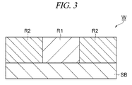
- the method MT can selectively etch a partial region of the wafer W as a target object depicted in FIG. 3 .
- the wafer W depicted in FIG. 3 includes a substrate SB, a first region R1, and a second region R2.
- the substrate SB is an underlying substrate for the first region R1 and the second region R2.
- the first region R1 is formed of silicon oxide and the second region R2 is formed of silicon nitride.
- the first region R1 and the second region R2 are exposed to plasma at the same time.
- the method MT may be performed to selectively etch the first region R1 with respect to the second region R2.
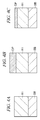
- FIG. 4A to FIG. 4C are diagrams explaining processes performed to the first region in the method MT.
- FIG. 5A to FIG. 5C are diagrams explaining processes performed to the second region in the method MT.
- the wafer W is exposed to plasma of a processing gas containing a fluorocarbon gas.
- the fluorocarbon gas includes at least one of, for example, a C 4 F 6 gas and a C 4 F 8 gas.
- the processing gas may include at least one of various rare gases such as an Ar gas and a He gas.
- the processing gas may include an oxygen (O 2 ) gas.
- the plasma is generated by exciting the processing gas, and the wafer W is exposed to the generated plasma.
- the processing gas is supplied into the processing chamber 12 from the gas source group 40. Further, in the process ST1, the high frequency power is supplied to the lower electrode LE from the first high frequency power supply 62. Further, in the process ST1, the high frequency bias power from the second high frequency power supply 64 may be supplied to the lower electrode LE. Furthermore, in the process ST1, a pressure of the space within the processing chamber 12 is set to be a preset pressure by the gas exhaust device 50. By way of example, the pressure of the space within the processing chamber 12 is set to be in a range of 20 mTorr (2.666 Pa) to 50 mTorr (6.666 Pa).
- a distance between the upper electrode 30 and the upper surface of the mounting table PD is set to be in a range of 20 mm to 50 mm.
- plasma of the processing gas is generated within the processing chamber 12, and the wafer W mounted on the mounting table PD is exposed to the plasma.
- a voltage from the power supply 70 may be applied to the upper electrode 30.
- the voltage applied from the power supply 70 to the upper electrode 30 may be -150 V or less. That is, the voltage applied from the power supply 70 to the upper electrode 30 may be a negative voltage having an absolute value of 150 V or more. While the process ST1 is performed, the operations of the respective components of the plasma processing apparatus 10 can be controlled by the control unit Cnt.
- active species of atoms and/or molecules generated from fluorocarbon collide with the first region R1 of the wafer W in a state as depicted in FIG. 4A .
- the first region R1 is etched.
- a deposit including fluorocarbon is deposited on the first region R1.
- a deposit DP including fluorocarbon is formed on the first region R1.
- a film thickness of the deposit DP is increased as a processing time of performing the process ST1 is increased.
- the active species of atoms and/or molecules generated from fluorocarbon collide with the second region R2 of the wafer W in a state as depicted in FIG. 5A .
- a modified region TR which has a large amount of carbon and is modified from the fluorocarbon deposit, may be formed on a surface of the second region R2.
- the modified region TR contains silicon and nitrogen forming the second region R2 and atoms and/or molecules included in the processing gas.
- the modified region TR may contain carbon, fluorine, and oxygen included in the processing gas in addition to silicon and nitrogen.
- the deposit DP is formed on the modified region TR.
- the positive ions within the processing space S collide with the electrode plate 34.
- silicon is released from the electrode plate 34.
- the released silicon is bonded to the active species of fluorine, for example, a fluorine radical and a fluorine ion, within the processing space S, so that the amount of the active species of fluorine is reduced.
- a forming rate of the modified region TR having a large amount of carbon is increased, and it is possible to suppress the second region R2 from being etched with the active species of fluorine.
- the first region R1 is etched with active species of fluorocarbon in the plasma, and the deposit DP of fluorocarbon is formed on the first region R1 by the active species of fluorocarbon.
- the deposit DP suppresses the active species capable of etching the first region R1 from reaching the first region R1. Therefore, if the process ST is continuously performed, the etching of the first region R1 is stopped. In order to suppress the etching from being stopped, the process ST2 is subsequently performed according to the method MT.
- the first region R1 is etched with a radical of fluorocarbon included in the deposit DP.
- the wafer W after the process ST1 is exposed to plasma of a rare gas.
- a processing time for the process ST2 and a processing time for the process ST1 can be appropriately set.
- the processing time for the process ST1 may be set to have a ratio in a range of 30% to 70% of the total processing time for the process ST1 and the process ST2.
- the rare gas is supplied from the gas source group 40. Further, in the process ST2, an oxygen gas (O 2 gas) may or may not be supplied together with the rare gas. Furthermore, in the process ST2, the high frequency power is applied to the lower electrode LE from the first high frequency power supply 62. Moreover, in the process ST2, the high frequency bias power from the second high frequency power supply 64 may be applied to the lower electrode LE. Further, in the process ST2, a pressure of the space within the processing chamber 12 is set to be a preset pressure by the gas exhaust device 50. By way of example, the pressure of the space within the processing chamber 12 is set to be in a range of 20 mTorr (2.666 Pa) to 50 mTorr (6.666 Pa).
- a distance between the upper electrode 30 and the upper surface of the mounting table PD is set to be in a range of 20 mm to 50 mm.
- plasma of the rare gas is generated within the processing chamber 12, and the wafer W mounted on the mounting table PD is exposed to the plasma.
- the voltage from the power supply 70 may be applied to the upper electrode 30.
- the voltage applied form the power supply 70 to the upper electrode 30 may be -150 V or less. That is, the voltage applied from the power supply 70 to the upper electrode 30 may be a negative voltage having an absolute value of 150 V or more. While the process ST2 is performed, the operations of the respective components of the plasma processing apparatus 10 can be controlled by the control unit Cnt.
- the process ST2 active species of rare gas atoms, for example, ions of rare gas atoms, collide with the deposit DP.
- the first region R1 is etched with the fluorocarbon radical in the deposit DP.
- the film thickness of the deposit DP is reduced through the process ST2.
- the film thickness of the deposit DP on the second region R2 is also reduced.
- the modified region TR is formed on the second region R2, the etching of the second region R2 is suppressed.
- the positive ions within the processing space S collide with the electrode plate 34.
- silicon is released from the electrode plate 34.
- the active species of fluorine generated through the process ST1 are not completely removed but may remain within the processing chamber 12.
- the silicon released from the electrode plate 34 is bonded to the active species of fluorine within the processing space S to reduce the amount of the active species of fluorine.
- the etching of the second region R2 with the active species of fluorine is suppressed.
- the first region R1 is etched with the radical of fluorocarbon in the deposit DP.
- the first region R1 may be further etched selectively with respect to the second region R2.
- the process ST1 is performed again. Since the film thickness of the deposit DP is reduced through the process ST2, if the wafer W is exposed to the plasma of the processing gas by performing the process ST1 again, the first region R1 can be further etched. Then, since the process ST2 is further performed, the first region R1 can be further etched with the radical of fluorocarbon in the deposit DP.
- a stop condition it is determined whether or not a stop condition is satisfied. It is determined that the stop condition is satisfied, for example, when the repetition number of a cycle including the process ST1 and the process ST2 reaches a preset number of times. If the stop condition is not satisfied, the cycle including the process ST1 and the process ST2 is performed again. On the other hand, if the stop condition is satisfied, the method MT is ended.
- the first region R1 can be selectively etched with respect to the second region R2.
- FIG. 6 is a cross-sectional view illustrating another example of a target object on which the method MT is performed.
- a wafer W2 depicted FIG. 6 includes a first region R1 and a second region R2, and the method MT can be performed on the wafer W2.
- the wafer W2 includes an underlying layer 100, multiple protruding regions 102, the first region R1, the second region R2, and a mask 108.
- the wafer W2 may be a product obtained, for example, during the manufacturing process of a fin-type field effect transistor.
- the underlying layer 100 may be formed of, for example, polycrystalline silicon.
- the underlying layer is a fin region, and has a substantially hexahedral shape.
- the multiple protruding regions 102 are formed on the underlying layer 100 and arranged to be substantially parallel to one another. These protruding regions 102 may be, for example, gate regions.
- the second region R2 is formed of silicon nitride to cover the protruding regions 102. Further, the multiple protruding regions 102 are buried in the first region R1. That is, the first region R1 is formed to cover the protruding regions 102 via the second region R2.
- the first region R1 is formed of silicon oxide.
- the mask 108 is formed on the first region R1.
- the mask 108 has a pattern in which an opening is formed above and between the adjacent protruding regions 102. This mask 108 is formed of an organic film. Further, the mask 108 can be formed by the photolithography.
- the first region R1 of the wafer W2 can be selectively etched with respect to the second region R2, so that a hole can be formed in a self-aligned manner between the adjacent protruding regions 102. Further, the first region R1 can be etched efficiently while suppressing the etching of the first region R1 from being stopped.
- the hole is extended to a surface of the underlying layer 100 through a region between the adjacent protruding regions 102.
- the hole may be, for example, a contact hole connected to a source or a drain in the fin region.
- the experimental examples 1 to 4 and the comparative experimental example 1 there is prepared a wafer having a structure in which a silicon oxide chip of a square of 30 mm and a silicon nitride chip of a square of 30 mm are attached to a substrate on which a resist film is formed. These two chips are arranged at the equal distance from a center of the wafer. Processes of the experimental examples 1 to 4 and the comparative experimental example 1 are performed to the wafer under processing conditions to be described below. In the experimental example 1, a cycle including the process ST1 for 6 seconds and the process ST2 for 6 seconds is repeated 5 times. In the experimental example 2, a cycle including the process ST1 for 3 seconds and the process ST2 for 3 seconds is repeated 10 times.
- a cycle including the process ST1 for 2 seconds and the process ST2 for 2 seconds is repeated 15 times.
- a cycle including the process ST1 for 1 second and the process ST2 for 1 second is repeated 30 times.
- the process ST1 is performed for 60 seconds under the following processing conditions for the process ST1.
- the same wafer as that in the experimental example 1 is prepared. Processes of the experimental examples 5 and 6 and the comparative experimental example 2 are performed to the wafer under processing conditions to be described below. Further, in the experimental example 5, a cycle including the process ST1 for 6 seconds and the process ST2 for 6 seconds is repeated 5 times. In the experimental example 6, a cycle including the process ST1 for 3 seconds and the process ST2 for 3 seconds is repeated 10 times. Furthermore, in the comparative experimental example 2, the process ST1 is performed for 60 seconds under the following processing conditions for the process ST1.
- the same wafer as that in the experimental example 1 is prepared. Processes of the experimental examples 7 and 8 and the comparative experimental example 3 are performed to the wafer under processing conditions to be described below. Further, in the experimental example 7, a cycle including the process ST1 for 6 seconds and the process ST2 for 6 seconds is repeated 5 times. In the experimental example 8, a cycle including the process ST1 for 3 seconds and the process ST2 for 3 seconds is repeated 10 times. Furthermore, in the comparative experimental example 3, the process ST1 is performed for 60 seconds under the following processing conditions for the process ST1.
- Variations in film thicknesses, i.e., etched amounts, of the silicon oxide chip and the silicon nitride chip through the processes of the above-described experimental examples and the comparative experimental examples are obtained. Further, a ratio of the etched amount of the silicon oxide chip with respect to the etched amount of the silicon nitride chip, i.e., selectivity, is obtained.
- Table 1 shows the etched amounts and the selectivities of the two chips in the experimental examples 1 to 4 and the comparative experimental example 1; Table 2 shows the etched amounts and the selectivities of the two chips in the experimental examples 5 and 6 and the comparative experimental example 2; and Table 3 shows the etched amounts and the selectivities of the two chips in the experimental examples 7 and 8 and the comparative experimental example 3.
- the etched amounts of the silicon oxide chips in the experimental examples 1 to 4 are greater than the etched amount of the silicon oxide chip in the comparative experimental example 1. From this result, according to the experimental examples 1 to 4 as exemplary experimental examples of the method MT, it is possible to continuously etch a region formed of silicon oxide. Further, by comparison between the selectivities in the experimental examples 1 to 4 and the selectivity in the comparative experimental example 1, the selectivities in the experimental examples 1 to 4 are increased. From this result, according to the experimental examples 1 to 4 as the exemplary experimental examples of the method MT, it is possible to improve a selectivity.
- the experimental examples 5 and 6 are experimental examples in which a kind of a fluorocarbon gas is changed from that in the experimental examples 1 to 4, and the comparative experimental example 2 is an experimental example in which a kind of a fluorocarbon gas is changed from that in the comparative experimental example 1.
- a result of the comparison between the experimental examples 5 and 6 and the comparative experimental example 2 is the same as the result of the comparison between the experimental examples 1 to 4 and the comparative experimental example 1. That is, according to the experimental examples 5 and 6 as exemplary experimental examples of the method MT, even if a kind of a fluorocarbon gas is changed, it is possible to continuously etch a region formed of silicon oxide and also possible to improve a selectivity.
- the experimental examples 7 and 8 are experimental examples in which a high frequency power and a high frequency bias power are changed from those in the experimental examples 1 to 4, and the comparative experimental example 3 is an experimental example in which a high frequency power and a high frequency bias power are changed from those in the comparative experimental example 1.
- a result of the comparison between the experimental examples 7 and 8 and the comparative experimental example 3 is the same as the result of the comparison between the experimental examples 1 to 4 and the comparative experimental example 1. That is, according to the experimental examples 7 and 8 as exemplary experimental examples of the method MT, even if a high frequency power and a high frequency bias power are changed, it is possible to continuously etch a region formed of silicon oxide and also possible to improve a selectivity.
- the same wafer as that of the experimental example 1 is prepared.
- a process is performed to the wafer under processing conditions to be described below. That is, in the experimental example 9, an oxygen gas (O 2 gas) is not supplied in the process ST2.
- the repetition number of the process ST1 and the process ST2 serves as a variable parameter. That is, in the experimental example 9, the total processing time for repetition of the process ST1 and the process ST2 is set to be a variable parameter.
- FIG. 7 shows a graph showing a result obtained from the experimental example 9.
- FIG. 7 shows an etched amount of a silicon oxide chip, i.e., an etched amount of silicon oxide, and an etched amount of a silicon nitride chip, i.e., an etched amount of silicon nitride.
- a horizontal axis represents a total processing time
- a vertical axis represents an etched amount.
- the etched amount of the silicon oxide chip increases and the etched amount of the silicon nitride chip is kept constant at a small value. That is, from the experimental example 9, it is found that a high selectivity is obtained.
- the capacitively coupled plasma processing apparatus 10 is illustrated as a plasma processing apparatus which can be used for performing the method MT, but a plasma processing apparatus using a certain plasma source can be used for performing the method MT.
- various plasma processing apparatuses e.g. , an inductively coupled plasma processing apparatus and a plasma processing apparatus using a surface wave, e.g., a microwave, as a plasma source can be used for performing the method MT.
Landscapes
- Chemical & Material Sciences (AREA)
- Engineering & Computer Science (AREA)
- Physics & Mathematics (AREA)
- Plasma & Fusion (AREA)
- Analytical Chemistry (AREA)
- Drying Of Semiconductors (AREA)
- Chemical Kinetics & Catalysis (AREA)
- Materials Engineering (AREA)
- Mechanical Engineering (AREA)
- Metallurgy (AREA)
- Organic Chemistry (AREA)
- General Chemical & Material Sciences (AREA)
Applications Claiming Priority (2)
| Application Number | Priority Date | Filing Date | Title |
|---|---|---|---|
| JP2014032945 | 2014-02-24 | ||
| JP2014136543A JP6396699B2 (ja) | 2014-02-24 | 2014-07-02 | エッチング方法 |
Publications (1)
| Publication Number | Publication Date |
|---|---|
| EP2911187A1 true EP2911187A1 (de) | 2015-08-26 |
Family
ID=52589251
Family Applications (1)
| Application Number | Title | Priority Date | Filing Date |
|---|---|---|---|
| EP15155980.4A Withdrawn EP2911187A1 (de) | 2014-02-24 | 2015-02-20 | Ätzverfahren |
Country Status (6)
| Country | Link |
|---|---|
| US (1) | US9396962B2 (de) |
| EP (1) | EP2911187A1 (de) |
| JP (1) | JP6396699B2 (de) |
| KR (1) | KR102356211B1 (de) |
| CN (1) | CN104867827B (de) |
| TW (1) | TWI657502B (de) |
Cited By (4)
| Publication number | Priority date | Publication date | Assignee | Title |
|---|---|---|---|---|
| EP3046137A1 (de) * | 2015-01-16 | 2016-07-20 | Tokyo Electron Limited | Ätzverfahren |
| EP3062338A1 (de) * | 2015-02-24 | 2016-08-31 | Tokyo Electron Limited | Ätzverfahren |
| US20210296134A1 (en) * | 2020-03-19 | 2021-09-23 | Tokyo Electron Limited | Method of etching and apparatus for plasma processing |
| EP3726567B1 (de) * | 2017-12-15 | 2025-01-22 | Tokyo Electron Limited | Plasmaätzverfahren und plasmaätzvorrichtung |
Families Citing this family (300)
| Publication number | Priority date | Publication date | Assignee | Title |
|---|---|---|---|---|
| US20130023129A1 (en) | 2011-07-20 | 2013-01-24 | Asm America, Inc. | Pressure transmitter for a semiconductor processing environment |
| US10714315B2 (en) | 2012-10-12 | 2020-07-14 | Asm Ip Holdings B.V. | Semiconductor reaction chamber showerhead |
| US20160376700A1 (en) | 2013-02-01 | 2016-12-29 | Asm Ip Holding B.V. | System for treatment of deposition reactor |
| US11015245B2 (en) | 2014-03-19 | 2021-05-25 | Asm Ip Holding B.V. | Gas-phase reactor and system having exhaust plenum and components thereof |
| JP6235981B2 (ja) * | 2014-07-01 | 2017-11-22 | 東京エレクトロン株式会社 | 被処理体を処理する方法 |
| US10858737B2 (en) | 2014-07-28 | 2020-12-08 | Asm Ip Holding B.V. | Showerhead assembly and components thereof |
| US10941490B2 (en) | 2014-10-07 | 2021-03-09 | Asm Ip Holding B.V. | Multiple temperature range susceptor, assembly, reactor and system including the susceptor, and methods of using the same |
| US10276355B2 (en) | 2015-03-12 | 2019-04-30 | Asm Ip Holding B.V. | Multi-zone reactor, system including the reactor, and method of using the same |
| US10458018B2 (en) | 2015-06-26 | 2019-10-29 | Asm Ip Holding B.V. | Structures including metal carbide material, devices including the structures, and methods of forming same |
| US10211308B2 (en) | 2015-10-21 | 2019-02-19 | Asm Ip Holding B.V. | NbMC layers |
| US11139308B2 (en) | 2015-12-29 | 2021-10-05 | Asm Ip Holding B.V. | Atomic layer deposition of III-V compounds to form V-NAND devices |
| US10529554B2 (en) | 2016-02-19 | 2020-01-07 | Asm Ip Holding B.V. | Method for forming silicon nitride film selectively on sidewalls or flat surfaces of trenches |
| US10343920B2 (en) | 2016-03-18 | 2019-07-09 | Asm Ip Holding B.V. | Aligned carbon nanotubes |
| US10367080B2 (en) | 2016-05-02 | 2019-07-30 | Asm Ip Holding B.V. | Method of forming a germanium oxynitride film |
| JP6670672B2 (ja) * | 2016-05-10 | 2020-03-25 | 東京エレクトロン株式会社 | エッチング方法 |
| JP6592400B2 (ja) * | 2016-05-19 | 2019-10-16 | 東京エレクトロン株式会社 | エッチング方法 |
| JP6606464B2 (ja) | 2016-05-20 | 2019-11-13 | 東京エレクトロン株式会社 | エッチング方法 |
| US11453943B2 (en) | 2016-05-25 | 2022-09-27 | Asm Ip Holding B.V. | Method for forming carbon-containing silicon/metal oxide or nitride film by ALD using silicon precursor and hydrocarbon precursor |
| JP6685179B2 (ja) | 2016-06-01 | 2020-04-22 | 東京エレクトロン株式会社 | 基板処理方法 |
| US10612137B2 (en) | 2016-07-08 | 2020-04-07 | Asm Ip Holdings B.V. | Organic reactants for atomic layer deposition |
| US9859151B1 (en) | 2016-07-08 | 2018-01-02 | Asm Ip Holding B.V. | Selective film deposition method to form air gaps |
| US9887082B1 (en) | 2016-07-28 | 2018-02-06 | Asm Ip Holding B.V. | Method and apparatus for filling a gap |
| US9812320B1 (en) | 2016-07-28 | 2017-11-07 | Asm Ip Holding B.V. | Method and apparatus for filling a gap |
| KR102532607B1 (ko) | 2016-07-28 | 2023-05-15 | 에이에스엠 아이피 홀딩 비.브이. | 기판 가공 장치 및 그 동작 방법 |
| US11532757B2 (en) | 2016-10-27 | 2022-12-20 | Asm Ip Holding B.V. | Deposition of charge trapping layers |
| US10714350B2 (en) | 2016-11-01 | 2020-07-14 | ASM IP Holdings, B.V. | Methods for forming a transition metal niobium nitride film on a substrate by atomic layer deposition and related semiconductor device structures |
| KR102546317B1 (ko) | 2016-11-15 | 2023-06-21 | 에이에스엠 아이피 홀딩 비.브이. | 기체 공급 유닛 및 이를 포함하는 기판 처리 장치 |
| KR102762543B1 (ko) | 2016-12-14 | 2025-02-05 | 에이에스엠 아이피 홀딩 비.브이. | 기판 처리 장치 |
| US11581186B2 (en) | 2016-12-15 | 2023-02-14 | Asm Ip Holding B.V. | Sequential infiltration synthesis apparatus |
| US11447861B2 (en) | 2016-12-15 | 2022-09-20 | Asm Ip Holding B.V. | Sequential infiltration synthesis apparatus and a method of forming a patterned structure |
| KR102700194B1 (ko) | 2016-12-19 | 2024-08-28 | 에이에스엠 아이피 홀딩 비.브이. | 기판 처리 장치 |
| US10269558B2 (en) | 2016-12-22 | 2019-04-23 | Asm Ip Holding B.V. | Method of forming a structure on a substrate |
| US11390950B2 (en) | 2017-01-10 | 2022-07-19 | Asm Ip Holding B.V. | Reactor system and method to reduce residue buildup during a film deposition process |
| US10468261B2 (en) | 2017-02-15 | 2019-11-05 | Asm Ip Holding B.V. | Methods for forming a metallic film on a substrate by cyclical deposition and related semiconductor device structures |
| US10529563B2 (en) | 2017-03-29 | 2020-01-07 | Asm Ip Holdings B.V. | Method for forming doped metal oxide films on a substrate by cyclical deposition and related semiconductor device structures |
| US10770286B2 (en) | 2017-05-08 | 2020-09-08 | Asm Ip Holdings B.V. | Methods for selectively forming a silicon nitride film on a substrate and related semiconductor device structures |
| US12040200B2 (en) | 2017-06-20 | 2024-07-16 | Asm Ip Holding B.V. | Semiconductor processing apparatus and methods for calibrating a semiconductor processing apparatus |
| US11306395B2 (en) | 2017-06-28 | 2022-04-19 | Asm Ip Holding B.V. | Methods for depositing a transition metal nitride film on a substrate by atomic layer deposition and related deposition apparatus |
| KR20190009245A (ko) | 2017-07-18 | 2019-01-28 | 에이에스엠 아이피 홀딩 비.브이. | 반도체 소자 구조물 형성 방법 및 관련된 반도체 소자 구조물 |
| US11374112B2 (en) | 2017-07-19 | 2022-06-28 | Asm Ip Holding B.V. | Method for depositing a group IV semiconductor and related semiconductor device structures |
| US10541333B2 (en) | 2017-07-19 | 2020-01-21 | Asm Ip Holding B.V. | Method for depositing a group IV semiconductor and related semiconductor device structures |
| US11018002B2 (en) | 2017-07-19 | 2021-05-25 | Asm Ip Holding B.V. | Method for selectively depositing a Group IV semiconductor and related semiconductor device structures |
| US10590535B2 (en) | 2017-07-26 | 2020-03-17 | Asm Ip Holdings B.V. | Chemical treatment, deposition and/or infiltration apparatus and method for using the same |
| TWI815813B (zh) | 2017-08-04 | 2023-09-21 | 荷蘭商Asm智慧財產控股公司 | 用於分配反應腔內氣體的噴頭總成 |
| US10770336B2 (en) | 2017-08-08 | 2020-09-08 | Asm Ip Holding B.V. | Substrate lift mechanism and reactor including same |
| US10692741B2 (en) | 2017-08-08 | 2020-06-23 | Asm Ip Holdings B.V. | Radiation shield |
| US11139191B2 (en) | 2017-08-09 | 2021-10-05 | Asm Ip Holding B.V. | Storage apparatus for storing cassettes for substrates and processing apparatus equipped therewith |
| US11769682B2 (en) | 2017-08-09 | 2023-09-26 | Asm Ip Holding B.V. | Storage apparatus for storing cassettes for substrates and processing apparatus equipped therewith |
| US11830730B2 (en) | 2017-08-29 | 2023-11-28 | Asm Ip Holding B.V. | Layer forming method and apparatus |
| KR102491945B1 (ko) | 2017-08-30 | 2023-01-26 | 에이에스엠 아이피 홀딩 비.브이. | 기판 처리 장치 |
| US11056344B2 (en) | 2017-08-30 | 2021-07-06 | Asm Ip Holding B.V. | Layer forming method |
| US11295980B2 (en) | 2017-08-30 | 2022-04-05 | Asm Ip Holding B.V. | Methods for depositing a molybdenum metal film over a dielectric surface of a substrate by a cyclical deposition process and related semiconductor device structures |
| JP6937644B2 (ja) | 2017-09-26 | 2021-09-22 | 東京エレクトロン株式会社 | プラズマ処理装置及びプラズマ処理方法 |
| US10658205B2 (en) | 2017-09-28 | 2020-05-19 | Asm Ip Holdings B.V. | Chemical dispensing apparatus and methods for dispensing a chemical to a reaction chamber |
| US10403504B2 (en) | 2017-10-05 | 2019-09-03 | Asm Ip Holding B.V. | Method for selectively depositing a metallic film on a substrate |
| US10923344B2 (en) | 2017-10-30 | 2021-02-16 | Asm Ip Holding B.V. | Methods for forming a semiconductor structure and related semiconductor structures |
| US11022879B2 (en) | 2017-11-24 | 2021-06-01 | Asm Ip Holding B.V. | Method of forming an enhanced unexposed photoresist layer |
| CN111316417B (zh) | 2017-11-27 | 2023-12-22 | 阿斯莫Ip控股公司 | 与批式炉偕同使用的用于储存晶圆匣的储存装置 |
| JP7206265B2 (ja) | 2017-11-27 | 2023-01-17 | エーエスエム アイピー ホールディング ビー.ブイ. | クリーン・ミニエンバイロメントを備える装置 |
| US10872771B2 (en) | 2018-01-16 | 2020-12-22 | Asm Ip Holding B. V. | Method for depositing a material film on a substrate within a reaction chamber by a cyclical deposition process and related device structures |
| CN111630203A (zh) | 2018-01-19 | 2020-09-04 | Asm Ip私人控股有限公司 | 通过等离子体辅助沉积来沉积间隙填充层的方法 |
| TWI799494B (zh) | 2018-01-19 | 2023-04-21 | 荷蘭商Asm 智慧財產控股公司 | 沈積方法 |
| US11081345B2 (en) | 2018-02-06 | 2021-08-03 | Asm Ip Holding B.V. | Method of post-deposition treatment for silicon oxide film |
| US10896820B2 (en) | 2018-02-14 | 2021-01-19 | Asm Ip Holding B.V. | Method for depositing a ruthenium-containing film on a substrate by a cyclical deposition process |
| JP7124098B2 (ja) | 2018-02-14 | 2022-08-23 | エーエスエム・アイピー・ホールディング・ベー・フェー | 周期的堆積プロセスにより基材上にルテニウム含有膜を堆積させる方法 |
| US10731249B2 (en) | 2018-02-15 | 2020-08-04 | Asm Ip Holding B.V. | Method of forming a transition metal containing film on a substrate by a cyclical deposition process, a method for supplying a transition metal halide compound to a reaction chamber, and related vapor deposition apparatus |
| KR102636427B1 (ko) | 2018-02-20 | 2024-02-13 | 에이에스엠 아이피 홀딩 비.브이. | 기판 처리 방법 및 장치 |
| US10975470B2 (en) | 2018-02-23 | 2021-04-13 | Asm Ip Holding B.V. | Apparatus for detecting or monitoring for a chemical precursor in a high temperature environment |
| US11473195B2 (en) | 2018-03-01 | 2022-10-18 | Asm Ip Holding B.V. | Semiconductor processing apparatus and a method for processing a substrate |
| US11629406B2 (en) | 2018-03-09 | 2023-04-18 | Asm Ip Holding B.V. | Semiconductor processing apparatus comprising one or more pyrometers for measuring a temperature of a substrate during transfer of the substrate |
| US11114283B2 (en) | 2018-03-16 | 2021-09-07 | Asm Ip Holding B.V. | Reactor, system including the reactor, and methods of manufacturing and using same |
| KR102646467B1 (ko) | 2018-03-27 | 2024-03-11 | 에이에스엠 아이피 홀딩 비.브이. | 기판 상에 전극을 형성하는 방법 및 전극을 포함하는 반도체 소자 구조 |
| US11088002B2 (en) | 2018-03-29 | 2021-08-10 | Asm Ip Holding B.V. | Substrate rack and a substrate processing system and method |
| US11230766B2 (en) | 2018-03-29 | 2022-01-25 | Asm Ip Holding B.V. | Substrate processing apparatus and method |
| KR102600229B1 (ko) | 2018-04-09 | 2023-11-10 | 에이에스엠 아이피 홀딩 비.브이. | 기판 지지 장치, 이를 포함하는 기판 처리 장치 및 기판 처리 방법 |
| KR102709511B1 (ko) | 2018-05-08 | 2024-09-24 | 에이에스엠 아이피 홀딩 비.브이. | 기판 상에 산화물 막을 주기적 증착 공정에 의해 증착하기 위한 방법 및 관련 소자 구조 |
| US12025484B2 (en) | 2018-05-08 | 2024-07-02 | Asm Ip Holding B.V. | Thin film forming method |
| US12272527B2 (en) | 2018-05-09 | 2025-04-08 | Asm Ip Holding B.V. | Apparatus for use with hydrogen radicals and method of using same |
| KR102596988B1 (ko) | 2018-05-28 | 2023-10-31 | 에이에스엠 아이피 홀딩 비.브이. | 기판 처리 방법 및 그에 의해 제조된 장치 |
| US11718913B2 (en) | 2018-06-04 | 2023-08-08 | Asm Ip Holding B.V. | Gas distribution system and reactor system including same |
| TWI840362B (zh) | 2018-06-04 | 2024-05-01 | 荷蘭商Asm Ip私人控股有限公司 | 水氣降低的晶圓處置腔室 |
| US11286562B2 (en) | 2018-06-08 | 2022-03-29 | Asm Ip Holding B.V. | Gas-phase chemical reactor and method of using same |
| KR102568797B1 (ko) | 2018-06-21 | 2023-08-21 | 에이에스엠 아이피 홀딩 비.브이. | 기판 처리 시스템 |
| US10797133B2 (en) | 2018-06-21 | 2020-10-06 | Asm Ip Holding B.V. | Method for depositing a phosphorus doped silicon arsenide film and related semiconductor device structures |
| KR20250134000A (ko) | 2018-06-27 | 2025-09-09 | 에이에스엠 아이피 홀딩 비.브이. | 금속 함유 재료를 형성하기 위한 주기적 증착 방법 및 금속 함유 재료를 포함하는 필름 및 구조체 |
| US11499222B2 (en) | 2018-06-27 | 2022-11-15 | Asm Ip Holding B.V. | Cyclic deposition methods for forming metal-containing material and films and structures including the metal-containing material |
| US10612136B2 (en) | 2018-06-29 | 2020-04-07 | ASM IP Holding, B.V. | Temperature-controlled flange and reactor system including same |
| US10755922B2 (en) | 2018-07-03 | 2020-08-25 | Asm Ip Holding B.V. | Method for depositing silicon-free carbon-containing film as gap-fill layer by pulse plasma-assisted deposition |
| US10388513B1 (en) | 2018-07-03 | 2019-08-20 | Asm Ip Holding B.V. | Method for depositing silicon-free carbon-containing film as gap-fill layer by pulse plasma-assisted deposition |
| US11053591B2 (en) | 2018-08-06 | 2021-07-06 | Asm Ip Holding B.V. | Multi-port gas injection system and reactor system including same |
| JP7198609B2 (ja) | 2018-08-21 | 2023-01-04 | 東京エレクトロン株式会社 | エッチング方法及びプラズマ処理装置 |
| US11430674B2 (en) | 2018-08-22 | 2022-08-30 | Asm Ip Holding B.V. | Sensor array, apparatus for dispensing a vapor phase reactant to a reaction chamber and related methods |
| JP7110034B2 (ja) * | 2018-08-24 | 2022-08-01 | 東京エレクトロン株式会社 | エッチングする方法及びプラズマ処理装置 |
| US11024523B2 (en) | 2018-09-11 | 2021-06-01 | Asm Ip Holding B.V. | Substrate processing apparatus and method |
| KR102707956B1 (ko) | 2018-09-11 | 2024-09-19 | 에이에스엠 아이피 홀딩 비.브이. | 박막 증착 방법 |
| US11049751B2 (en) | 2018-09-14 | 2021-06-29 | Asm Ip Holding B.V. | Cassette supply system to store and handle cassettes and processing apparatus equipped therewith |
| CN110970344B (zh) | 2018-10-01 | 2024-10-25 | Asmip控股有限公司 | 衬底保持设备、包含所述设备的系统及其使用方法 |
| US11232963B2 (en) | 2018-10-03 | 2022-01-25 | Asm Ip Holding B.V. | Substrate processing apparatus and method |
| KR102592699B1 (ko) | 2018-10-08 | 2023-10-23 | 에이에스엠 아이피 홀딩 비.브이. | 기판 지지 유닛 및 이를 포함하는 박막 증착 장치와 기판 처리 장치 |
| KR102546322B1 (ko) | 2018-10-19 | 2023-06-21 | 에이에스엠 아이피 홀딩 비.브이. | 기판 처리 장치 및 기판 처리 방법 |
| KR102605121B1 (ko) | 2018-10-19 | 2023-11-23 | 에이에스엠 아이피 홀딩 비.브이. | 기판 처리 장치 및 기판 처리 방법 |
| USD948463S1 (en) | 2018-10-24 | 2022-04-12 | Asm Ip Holding B.V. | Susceptor for semiconductor substrate supporting apparatus |
| US12378665B2 (en) | 2018-10-26 | 2025-08-05 | Asm Ip Holding B.V. | High temperature coatings for a preclean and etch apparatus and related methods |
| US11087997B2 (en) | 2018-10-31 | 2021-08-10 | Asm Ip Holding B.V. | Substrate processing apparatus for processing substrates |
| KR102748291B1 (ko) | 2018-11-02 | 2024-12-31 | 에이에스엠 아이피 홀딩 비.브이. | 기판 지지 유닛 및 이를 포함하는 기판 처리 장치 |
| US11572620B2 (en) | 2018-11-06 | 2023-02-07 | Asm Ip Holding B.V. | Methods for selectively depositing an amorphous silicon film on a substrate |
| US11031242B2 (en) | 2018-11-07 | 2021-06-08 | Asm Ip Holding B.V. | Methods for depositing a boron doped silicon germanium film |
| US10847366B2 (en) | 2018-11-16 | 2020-11-24 | Asm Ip Holding B.V. | Methods for depositing a transition metal chalcogenide film on a substrate by a cyclical deposition process |
| US10818758B2 (en) | 2018-11-16 | 2020-10-27 | Asm Ip Holding B.V. | Methods for forming a metal silicate film on a substrate in a reaction chamber and related semiconductor device structures |
| US12040199B2 (en) | 2018-11-28 | 2024-07-16 | Asm Ip Holding B.V. | Substrate processing apparatus for processing substrates |
| US11217444B2 (en) | 2018-11-30 | 2022-01-04 | Asm Ip Holding B.V. | Method for forming an ultraviolet radiation responsive metal oxide-containing film |
| KR102636428B1 (ko) | 2018-12-04 | 2024-02-13 | 에이에스엠 아이피 홀딩 비.브이. | 기판 처리 장치를 세정하는 방법 |
| US11158513B2 (en) | 2018-12-13 | 2021-10-26 | Asm Ip Holding B.V. | Methods for forming a rhenium-containing film on a substrate by a cyclical deposition process and related semiconductor device structures |
| JP7504584B2 (ja) | 2018-12-14 | 2024-06-24 | エーエスエム・アイピー・ホールディング・ベー・フェー | 窒化ガリウムの選択的堆積を用いてデバイス構造体を形成する方法及びそのためのシステム |
| US11721595B2 (en) | 2019-01-11 | 2023-08-08 | Tokyo Electron Limited | Processing method and plasma processing apparatus |
| JP7258562B2 (ja) | 2019-01-11 | 2023-04-17 | 東京エレクトロン株式会社 | 処理方法及びプラズマ処理装置 |
| KR102841591B1 (ko) | 2019-01-11 | 2025-08-01 | 도쿄엘렉트론가부시키가이샤 | 처리 방법 및 플라즈마 처리 장치 |
| TWI819180B (zh) | 2019-01-17 | 2023-10-21 | 荷蘭商Asm 智慧財產控股公司 | 藉由循環沈積製程於基板上形成含過渡金屬膜之方法 |
| JP7174634B2 (ja) | 2019-01-18 | 2022-11-17 | 東京エレクトロン株式会社 | 膜をエッチングする方法 |
| KR102727227B1 (ko) | 2019-01-22 | 2024-11-07 | 에이에스엠 아이피 홀딩 비.브이. | 기판 처리 장치 |
| CN111524788B (zh) | 2019-02-01 | 2023-11-24 | Asm Ip私人控股有限公司 | 氧化硅的拓扑选择性膜形成的方法 |
| US11482533B2 (en) | 2019-02-20 | 2022-10-25 | Asm Ip Holding B.V. | Apparatus and methods for plug fill deposition in 3-D NAND applications |
| KR102638425B1 (ko) | 2019-02-20 | 2024-02-21 | 에이에스엠 아이피 홀딩 비.브이. | 기판 표면 내에 형성된 오목부를 충진하기 위한 방법 및 장치 |
| TWI845607B (zh) | 2019-02-20 | 2024-06-21 | 荷蘭商Asm Ip私人控股有限公司 | 用來填充形成於基材表面內之凹部的循環沉積方法及設備 |
| KR102626263B1 (ko) | 2019-02-20 | 2024-01-16 | 에이에스엠 아이피 홀딩 비.브이. | 처리 단계를 포함하는 주기적 증착 방법 및 이를 위한 장치 |
| TWI842826B (zh) | 2019-02-22 | 2024-05-21 | 荷蘭商Asm Ip私人控股有限公司 | 基材處理設備及處理基材之方法 |
| KR102762833B1 (ko) | 2019-03-08 | 2025-02-04 | 에이에스엠 아이피 홀딩 비.브이. | SiOCN 층을 포함한 구조체 및 이의 형성 방법 |
| KR102782593B1 (ko) | 2019-03-08 | 2025-03-14 | 에이에스엠 아이피 홀딩 비.브이. | SiOC 층을 포함한 구조체 및 이의 형성 방법 |
| KR102858005B1 (ko) | 2019-03-08 | 2025-09-09 | 에이에스엠 아이피 홀딩 비.브이. | 실리콘 질화물 층을 선택적으로 증착하는 방법, 및 선택적으로 증착된 실리콘 질화물 층을 포함하는 구조체 |
| JP2020167398A (ja) | 2019-03-28 | 2020-10-08 | エーエスエム・アイピー・ホールディング・ベー・フェー | ドアオープナーおよびドアオープナーが提供される基材処理装置 |
| KR102809999B1 (ko) | 2019-04-01 | 2025-05-19 | 에이에스엠 아이피 홀딩 비.브이. | 반도체 소자를 제조하는 방법 |
| US11447864B2 (en) | 2019-04-19 | 2022-09-20 | Asm Ip Holding B.V. | Layer forming method and apparatus |
| KR20200125453A (ko) | 2019-04-24 | 2020-11-04 | 에이에스엠 아이피 홀딩 비.브이. | 기상 반응기 시스템 및 이를 사용하는 방법 |
| KR102869364B1 (ko) | 2019-05-07 | 2025-10-10 | 에이에스엠 아이피 홀딩 비.브이. | 비정질 탄소 중합체 막을 개질하는 방법 |
| KR102929471B1 (ko) | 2019-05-07 | 2026-02-20 | 에이에스엠 아이피 홀딩 비.브이. | 딥 튜브가 있는 화학물질 공급원 용기 |
| KR102929472B1 (ko) | 2019-05-10 | 2026-02-20 | 에이에스엠 아이피 홀딩 비.브이. | 표면 상에 재료를 증착하는 방법 및 본 방법에 따라 형성된 구조 |
| JP7598201B2 (ja) | 2019-05-16 | 2024-12-11 | エーエスエム・アイピー・ホールディング・ベー・フェー | ウェハボートハンドリング装置、縦型バッチ炉および方法 |
| JP7612342B2 (ja) | 2019-05-16 | 2025-01-14 | エーエスエム・アイピー・ホールディング・ベー・フェー | ウェハボートハンドリング装置、縦型バッチ炉および方法 |
| USD975665S1 (en) | 2019-05-17 | 2023-01-17 | Asm Ip Holding B.V. | Susceptor shaft |
| USD947913S1 (en) | 2019-05-17 | 2022-04-05 | Asm Ip Holding B.V. | Susceptor shaft |
| USD935572S1 (en) | 2019-05-24 | 2021-11-09 | Asm Ip Holding B.V. | Gas channel plate |
| USD922229S1 (en) | 2019-06-05 | 2021-06-15 | Asm Ip Holding B.V. | Device for controlling a temperature of a gas supply unit |
| KR20200141003A (ko) | 2019-06-06 | 2020-12-17 | 에이에스엠 아이피 홀딩 비.브이. | 가스 감지기를 포함하는 기상 반응기 시스템 |
| KR102918757B1 (ko) | 2019-06-10 | 2026-01-28 | 에이에스엠 아이피 홀딩 비.브이. | 석영 에피택셜 챔버를 세정하는 방법 |
| KR20200143254A (ko) | 2019-06-11 | 2020-12-23 | 에이에스엠 아이피 홀딩 비.브이. | 개질 가스를 사용하여 전자 구조를 형성하는 방법, 상기 방법을 수행하기 위한 시스템, 및 상기 방법을 사용하여 형성되는 구조 |
| TWI848120B (zh) | 2019-06-13 | 2024-07-11 | 日商東京威力科創股份有限公司 | 蝕刻方法以及蝕刻裝置 |
| USD944946S1 (en) | 2019-06-14 | 2022-03-01 | Asm Ip Holding B.V. | Shower plate |
| USD931978S1 (en) | 2019-06-27 | 2021-09-28 | Asm Ip Holding B.V. | Showerhead vacuum transport |
| KR102911421B1 (ko) | 2019-07-03 | 2026-01-12 | 에이에스엠 아이피 홀딩 비.브이. | 기판 처리 장치용 온도 제어 조립체 및 이를 사용하는 방법 |
| JP7499079B2 (ja) | 2019-07-09 | 2024-06-13 | エーエスエム・アイピー・ホールディング・ベー・フェー | 同軸導波管を用いたプラズマ装置、基板処理方法 |
| CN112216646B (zh) | 2019-07-10 | 2026-02-10 | Asmip私人控股有限公司 | 基板支撑组件及包括其的基板处理装置 |
| KR102895115B1 (ko) | 2019-07-16 | 2025-12-03 | 에이에스엠 아이피 홀딩 비.브이. | 기판 처리 장치 |
| KR102860110B1 (ko) | 2019-07-17 | 2025-09-16 | 에이에스엠 아이피 홀딩 비.브이. | 실리콘 게르마늄 구조를 형성하는 방법 |
| KR102955799B1 (ko) | 2019-07-17 | 2026-04-21 | 에이에스엠 아이피 홀딩 비.브이. | 라디칼 보조 점화 플라즈마 시스템 및 방법 |
| US11643724B2 (en) | 2019-07-18 | 2023-05-09 | Asm Ip Holding B.V. | Method of forming structures using a neutral beam |
| TWI839544B (zh) | 2019-07-19 | 2024-04-21 | 荷蘭商Asm Ip私人控股有限公司 | 形成形貌受控的非晶碳聚合物膜之方法 |
| KR102903090B1 (ko) | 2019-07-19 | 2025-12-19 | 에이에스엠 아이피 홀딩 비.브이. | 토폴로지-제어된 비정질 탄소 중합체 막을 형성하는 방법 |
| TWI851767B (zh) | 2019-07-29 | 2024-08-11 | 荷蘭商Asm Ip私人控股有限公司 | 用於利用n型摻雜物及/或替代摻雜物選擇性沉積以達成高摻雜物併入之方法 |
| KR20210015655A (ko) | 2019-07-30 | 2021-02-10 | 에이에스엠 아이피 홀딩 비.브이. | 기판 처리 장치 및 방법 |
| CN112309900B (zh) | 2019-07-30 | 2025-11-04 | Asmip私人控股有限公司 | 基板处理设备 |
| CN112309899B (zh) | 2019-07-30 | 2025-11-14 | Asmip私人控股有限公司 | 基板处理设备 |
| US11227782B2 (en) | 2019-07-31 | 2022-01-18 | Asm Ip Holding B.V. | Vertical batch furnace assembly |
| US11587814B2 (en) | 2019-07-31 | 2023-02-21 | Asm Ip Holding B.V. | Vertical batch furnace assembly |
| US11587815B2 (en) | 2019-07-31 | 2023-02-21 | Asm Ip Holding B.V. | Vertical batch furnace assembly |
| US12622218B2 (en) | 2019-07-31 | 2026-05-05 | Asm Ip Holding B.V. | Cassette lid opening device |
| CN112323048B (zh) | 2019-08-05 | 2024-02-09 | Asm Ip私人控股有限公司 | 用于化学源容器的液位传感器 |
| KR20210018761A (ko) | 2019-08-09 | 2021-02-18 | 에이에스엠 아이피 홀딩 비.브이. | 냉각 장치를 포함한 히터 어셈블리 및 이를 사용하는 방법 |
| USD965044S1 (en) | 2019-08-19 | 2022-09-27 | Asm Ip Holding B.V. | Susceptor shaft |
| USD965524S1 (en) | 2019-08-19 | 2022-10-04 | Asm Ip Holding B.V. | Susceptor support |
| JP7810514B2 (ja) | 2019-08-21 | 2026-02-03 | エーエスエム・アイピー・ホールディング・ベー・フェー | 成膜原料混合ガス生成装置及び成膜装置 |
| USD930782S1 (en) | 2019-08-22 | 2021-09-14 | Asm Ip Holding B.V. | Gas distributor |
| USD979506S1 (en) | 2019-08-22 | 2023-02-28 | Asm Ip Holding B.V. | Insulator |
| USD940837S1 (en) | 2019-08-22 | 2022-01-11 | Asm Ip Holding B.V. | Electrode |
| USD949319S1 (en) | 2019-08-22 | 2022-04-19 | Asm Ip Holding B.V. | Exhaust duct |
| KR20210024423A (ko) | 2019-08-22 | 2021-03-05 | 에이에스엠 아이피 홀딩 비.브이. | 홀을 구비한 구조체를 형성하기 위한 방법 |
| US11286558B2 (en) | 2019-08-23 | 2022-03-29 | Asm Ip Holding B.V. | Methods for depositing a molybdenum nitride film on a surface of a substrate by a cyclical deposition process and related semiconductor device structures including a molybdenum nitride film |
| KR102928101B1 (ko) | 2019-08-23 | 2026-02-13 | 에이에스엠 아이피 홀딩 비.브이. | 비스(디에틸아미노)실란을 사용하여 peald에 의해 개선된 품질을 갖는 실리콘 산화물 막을 증착하기 위한 방법 |
| CN112442674A (zh) | 2019-09-03 | 2021-03-05 | Asm Ip私人控股有限公司 | 用于沉积硫族化物膜的方法和设备以及包括膜的结构 |
| KR102806450B1 (ko) | 2019-09-04 | 2025-05-12 | 에이에스엠 아이피 홀딩 비.브이. | 희생 캡핑 층을 이용한 선택적 증착 방법 |
| KR102733104B1 (ko) | 2019-09-05 | 2024-11-22 | 에이에스엠 아이피 홀딩 비.브이. | 기판 처리 장치 |
| US12469693B2 (en) | 2019-09-17 | 2025-11-11 | Asm Ip Holding B.V. | Method of forming a carbon-containing layer and structure including the layer |
| US11562901B2 (en) | 2019-09-25 | 2023-01-24 | Asm Ip Holding B.V. | Substrate processing method |
| JP7398915B2 (ja) | 2019-10-01 | 2023-12-15 | 東京エレクトロン株式会社 | 基板処理方法、半導体デバイスの製造方法、及び、プラズマ処理装置 |
| CN112593212B (zh) | 2019-10-02 | 2023-12-22 | Asm Ip私人控股有限公司 | 通过循环等离子体增强沉积工艺形成拓扑选择性氧化硅膜的方法 |
| TWI846953B (zh) | 2019-10-08 | 2024-07-01 | 荷蘭商Asm Ip私人控股有限公司 | 基板處理裝置 |
| US12428726B2 (en) | 2019-10-08 | 2025-09-30 | Asm Ip Holding B.V. | Gas injection system and reactor system including same |
| KR102948143B1 (ko) | 2019-10-08 | 2026-04-07 | 에이에스엠 아이피 홀딩 비.브이. | 활성 종을 이용하기 위한 가스 분배 어셈블리를 포함한 반응기 시스템 및 이를 사용하는 방법 |
| TWI846966B (zh) | 2019-10-10 | 2024-07-01 | 荷蘭商Asm Ip私人控股有限公司 | 形成光阻底層之方法及包括光阻底層之結構 |
| US12009241B2 (en) | 2019-10-14 | 2024-06-11 | Asm Ip Holding B.V. | Vertical batch furnace assembly with detector to detect cassette |
| TWI834919B (zh) | 2019-10-16 | 2024-03-11 | 荷蘭商Asm Ip私人控股有限公司 | 氧化矽之拓撲選擇性膜形成之方法 |
| US11637014B2 (en) | 2019-10-17 | 2023-04-25 | Asm Ip Holding B.V. | Methods for selective deposition of doped semiconductor material |
| KR102845724B1 (ko) | 2019-10-21 | 2025-08-13 | 에이에스엠 아이피 홀딩 비.브이. | 막을 선택적으로 에칭하기 위한 장치 및 방법 |
| US11996292B2 (en) | 2019-10-25 | 2024-05-28 | Asm Ip Holding B.V. | Methods for filling a gap feature on a substrate surface and related semiconductor structures |
| US11646205B2 (en) | 2019-10-29 | 2023-05-09 | Asm Ip Holding B.V. | Methods of selectively forming n-type doped material on a surface, systems for selectively forming n-type doped material, and structures formed using same |
| KR102890638B1 (ko) | 2019-11-05 | 2025-11-25 | 에이에스엠 아이피 홀딩 비.브이. | 도핑된 반도체 층을 갖는 구조체 및 이를 형성하기 위한 방법 및 시스템 |
| US11501968B2 (en) | 2019-11-15 | 2022-11-15 | Asm Ip Holding B.V. | Method for providing a semiconductor device with silicon filled gaps |
| KR102861314B1 (ko) | 2019-11-20 | 2025-09-17 | 에이에스엠 아이피 홀딩 비.브이. | 기판의 표면 상에 탄소 함유 물질을 증착하는 방법, 상기 방법을 사용하여 형성된 구조물, 및 상기 구조물을 형성하기 위한 시스템 |
| CN112951697B (zh) | 2019-11-26 | 2025-07-29 | Asmip私人控股有限公司 | 基板处理设备 |
| KR20210065848A (ko) | 2019-11-26 | 2021-06-04 | 에이에스엠 아이피 홀딩 비.브이. | 제1 유전체 표면과 제2 금속성 표면을 포함한 기판 상에 타겟 막을 선택적으로 형성하기 위한 방법 |
| CN120998766A (zh) | 2019-11-29 | 2025-11-21 | Asm Ip私人控股有限公司 | 基板处理设备 |
| CN120432376A (zh) | 2019-11-29 | 2025-08-05 | Asm Ip私人控股有限公司 | 基板处理设备 |
| JP7527928B2 (ja) | 2019-12-02 | 2024-08-05 | エーエスエム・アイピー・ホールディング・ベー・フェー | 基板処理装置、基板処理方法 |
| KR20210070898A (ko) | 2019-12-04 | 2021-06-15 | 에이에스엠 아이피 홀딩 비.브이. | 기판 처리 장치 |
| JPWO2021117534A1 (de) | 2019-12-12 | 2021-06-17 | ||
| JP7703317B2 (ja) | 2019-12-17 | 2025-07-07 | エーエスエム・アイピー・ホールディング・ベー・フェー | 窒化バナジウム層および窒化バナジウム層を含む構造体を形成する方法 |
| KR102943768B1 (ko) | 2019-12-19 | 2026-03-26 | 에이에스엠 아이피 홀딩 비.브이. | 기판 상의 갭 피처를 충진하는 방법 및 이와 관련된 반도체 소자 구조 |
| TWI887322B (zh) | 2020-01-06 | 2025-06-21 | 荷蘭商Asm Ip私人控股有限公司 | 反應器系統、抬升銷、及處理方法 |
| TWI901623B (zh) | 2020-01-06 | 2025-10-21 | 荷蘭商Asm Ip私人控股有限公司 | 氣體供應總成以及閥板總成 |
| US11993847B2 (en) | 2020-01-08 | 2024-05-28 | Asm Ip Holding B.V. | Injector |
| KR102882467B1 (ko) | 2020-01-16 | 2025-11-05 | 에이에스엠 아이피 홀딩 비.브이. | 고 종횡비 피처를 형성하는 방법 |
| KR102675856B1 (ko) | 2020-01-20 | 2024-06-17 | 에이에스엠 아이피 홀딩 비.브이. | 박막 형성 방법 및 박막 표면 개질 방법 |
| TWI889744B (zh) | 2020-01-29 | 2025-07-11 | 荷蘭商Asm Ip私人控股有限公司 | 污染物捕集系統、及擋板堆疊 |
| TWI871421B (zh) | 2020-02-03 | 2025-02-01 | 荷蘭商Asm Ip私人控股有限公司 | 包括釩或銦層的裝置、結構及其形成方法、系統 |
| KR20210100010A (ko) | 2020-02-04 | 2021-08-13 | 에이에스엠 아이피 홀딩 비.브이. | 대형 물품의 투과율 측정을 위한 방법 및 장치 |
| US11776846B2 (en) | 2020-02-07 | 2023-10-03 | Asm Ip Holding B.V. | Methods for depositing gap filling fluids and related systems and devices |
| KR20210103953A (ko) | 2020-02-13 | 2021-08-24 | 에이에스엠 아이피 홀딩 비.브이. | 가스 분배 어셈블리 및 이를 사용하는 방법 |
| KR102916725B1 (ko) | 2020-02-13 | 2026-01-23 | 에이에스엠 아이피 홀딩 비.브이. | 수광 장치를 포함하는 기판 처리 장치 및 수광 장치의 교정 방법 |
| US11781243B2 (en) | 2020-02-17 | 2023-10-10 | Asm Ip Holding B.V. | Method for depositing low temperature phosphorous-doped silicon |
| TWI895326B (zh) | 2020-02-28 | 2025-09-01 | 荷蘭商Asm Ip私人控股有限公司 | 專用於零件清潔的系統 |
| TWI914330B (zh) | 2020-03-04 | 2026-02-11 | 荷蘭商Asm Ip私人控股有限公司 | 反應器系統、及對準夾具 |
| KR20210116240A (ko) | 2020-03-11 | 2021-09-27 | 에이에스엠 아이피 홀딩 비.브이. | 조절성 접합부를 갖는 기판 핸들링 장치 |
| KR20210116249A (ko) | 2020-03-11 | 2021-09-27 | 에이에스엠 아이피 홀딩 비.브이. | 록아웃 태그아웃 어셈블리 및 시스템 그리고 이의 사용 방법 |
| CN113394086A (zh) | 2020-03-12 | 2021-09-14 | Asm Ip私人控股有限公司 | 用于制造具有目标拓扑轮廓的层结构的方法 |
| US12173404B2 (en) | 2020-03-17 | 2024-12-24 | Asm Ip Holding B.V. | Method of depositing epitaxial material, structure formed using the method, and system for performing the method |
| JP7433095B2 (ja) | 2020-03-18 | 2024-02-19 | 東京エレクトロン株式会社 | 基板処理方法及び基板処理装置 |
| KR102755229B1 (ko) | 2020-04-02 | 2025-01-14 | 에이에스엠 아이피 홀딩 비.브이. | 박막 형성 방법 |
| TWI887376B (zh) | 2020-04-03 | 2025-06-21 | 荷蘭商Asm Ip私人控股有限公司 | 半導體裝置的製造方法 |
| TWI888525B (zh) | 2020-04-08 | 2025-07-01 | 荷蘭商Asm Ip私人控股有限公司 | 用於選擇性蝕刻氧化矽膜之設備及方法 |
| KR20210128343A (ko) | 2020-04-15 | 2021-10-26 | 에이에스엠 아이피 홀딩 비.브이. | 크롬 나이트라이드 층을 형성하는 방법 및 크롬 나이트라이드 층을 포함하는 구조 |
| US11821078B2 (en) | 2020-04-15 | 2023-11-21 | Asm Ip Holding B.V. | Method for forming precoat film and method for forming silicon-containing film |
| US11996289B2 (en) | 2020-04-16 | 2024-05-28 | Asm Ip Holding B.V. | Methods of forming structures including silicon germanium and silicon layers, devices formed using the methods, and systems for performing the methods |
| KR102901748B1 (ko) | 2020-04-21 | 2025-12-17 | 에이에스엠 아이피 홀딩 비.브이. | 기판을 처리하기 위한 방법 |
| KR20210132612A (ko) | 2020-04-24 | 2021-11-04 | 에이에스엠 아이피 홀딩 비.브이. | 바나듐 화합물들을 안정화하기 위한 방법들 및 장치 |
| KR20210132600A (ko) | 2020-04-24 | 2021-11-04 | 에이에스엠 아이피 홀딩 비.브이. | 바나듐, 질소 및 추가 원소를 포함한 층을 증착하기 위한 방법 및 시스템 |
| US11898243B2 (en) | 2020-04-24 | 2024-02-13 | Asm Ip Holding B.V. | Method of forming vanadium nitride-containing layer |
| KR102934380B1 (ko) | 2020-04-24 | 2026-03-05 | 에이에스엠 아이피 홀딩 비.브이. | 바나듐 보라이드 및 바나듐 포스파이드 층을 포함한 구조체를 형성하는 방법 |
| KR102866804B1 (ko) | 2020-04-24 | 2025-09-30 | 에이에스엠 아이피 홀딩 비.브이. | 냉각 가스 공급부를 포함한 수직형 배치 퍼니스 어셈블리 |
| KR102783898B1 (ko) | 2020-04-29 | 2025-03-18 | 에이에스엠 아이피 홀딩 비.브이. | 고체 소스 전구체 용기 |
| KR20210134869A (ko) | 2020-05-01 | 2021-11-11 | 에이에스엠 아이피 홀딩 비.브이. | Foup 핸들러를 이용한 foup의 빠른 교환 |
| JP7726664B2 (ja) | 2020-05-04 | 2025-08-20 | エーエスエム・アイピー・ホールディング・ベー・フェー | 基板を処理するための基板処理システム |
| JP7736446B2 (ja) | 2020-05-07 | 2025-09-09 | エーエスエム・アイピー・ホールディング・ベー・フェー | 同調回路を備える反応器システム |
| KR102788543B1 (ko) | 2020-05-13 | 2025-03-27 | 에이에스엠 아이피 홀딩 비.브이. | 반응기 시스템용 레이저 정렬 고정구 |
| TWI915365B (zh) | 2020-05-15 | 2026-02-21 | 荷蘭商Asm Ip私人控股有限公司 | 形成矽鍺層之方法、半導體結構、半導體裝置、形成沉積層之方法、及沉積系統 |
| TWI911214B (zh) | 2020-05-19 | 2026-01-11 | 荷蘭商Asm Ip私人控股有限公司 | 基材處理設備 |
| KR102795476B1 (ko) | 2020-05-21 | 2025-04-11 | 에이에스엠 아이피 홀딩 비.브이. | 다수의 탄소 층을 포함한 구조체 및 이를 형성하고 사용하는 방법 |
| KR20210145079A (ko) | 2020-05-21 | 2021-12-01 | 에이에스엠 아이피 홀딩 비.브이. | 기판을 처리하기 위한 플랜지 및 장치 |
| TWI873343B (zh) | 2020-05-22 | 2025-02-21 | 荷蘭商Asm Ip私人控股有限公司 | 用於在基材上形成薄膜之反應系統 |
| KR20210146802A (ko) | 2020-05-26 | 2021-12-06 | 에이에스엠 아이피 홀딩 비.브이. | 붕소 및 갈륨을 함유한 실리콘 게르마늄 층을 증착하는 방법 |
| TWI876048B (zh) | 2020-05-29 | 2025-03-11 | 荷蘭商Asm Ip私人控股有限公司 | 基板處理方法 |
| TW202212620A (zh) | 2020-06-02 | 2022-04-01 | 荷蘭商Asm Ip私人控股有限公司 | 處理基板之設備、形成膜之方法、及控制用於處理基板之設備之方法 |
| KR20210156219A (ko) | 2020-06-16 | 2021-12-24 | 에이에스엠 아이피 홀딩 비.브이. | 붕소를 함유한 실리콘 게르마늄 층을 증착하는 방법 |
| TWI908816B (zh) | 2020-06-24 | 2025-12-21 | 荷蘭商Asm Ip私人控股有限公司 | 形成含矽層之方法 |
| TWI873359B (zh) | 2020-06-30 | 2025-02-21 | 荷蘭商Asm Ip私人控股有限公司 | 基板處理方法 |
| TWI896694B (zh) | 2020-07-01 | 2025-09-11 | 荷蘭商Asm Ip私人控股有限公司 | 沉積方法、半導體結構、及沉積系統 |
| TW202202649A (zh) | 2020-07-08 | 2022-01-16 | 荷蘭商Asm Ip私人控股有限公司 | 基板處理方法 |
| TWI864307B (zh) | 2020-07-17 | 2024-12-01 | 荷蘭商Asm Ip私人控股有限公司 | 用於光微影之結構、方法與系統 |
| KR20220011092A (ko) | 2020-07-20 | 2022-01-27 | 에이에스엠 아이피 홀딩 비.브이. | 전이 금속층을 포함하는 구조체를 형성하기 위한 방법 및 시스템 |
| TWI878570B (zh) | 2020-07-20 | 2025-04-01 | 荷蘭商Asm Ip私人控股有限公司 | 用於沉積鉬層之方法及系統 |
| US12322591B2 (en) | 2020-07-27 | 2025-06-03 | Asm Ip Holding B.V. | Thin film deposition process |
| TW202605918A (zh) | 2020-08-11 | 2026-02-01 | 荷蘭商Asm Ip私人控股有限公司 | 閘極堆疊 |
| KR102915124B1 (ko) | 2020-08-14 | 2026-01-19 | 에이에스엠 아이피 홀딩 비.브이. | 기판 처리 방법 |
| US12040177B2 (en) | 2020-08-18 | 2024-07-16 | Asm Ip Holding B.V. | Methods for forming a laminate film by cyclical plasma-enhanced deposition processes |
| JP7450494B2 (ja) | 2020-08-18 | 2024-03-15 | 東京エレクトロン株式会社 | 基板処理装置および基板処理装置のガス切り替え方法 |
| TWI911263B (zh) | 2020-08-25 | 2026-01-11 | 荷蘭商Asm Ip私人控股有限公司 | 清潔基板的方法、選擇性沉積的方法、及反應器系統 |
| US11725280B2 (en) | 2020-08-26 | 2023-08-15 | Asm Ip Holding B.V. | Method for forming metal silicon oxide and metal silicon oxynitride layers |
| TWI911265B (zh) | 2020-08-27 | 2026-01-11 | 荷蘭商Asm Ip私人控股有限公司 | 形成圖案化結構的方法、操控機械特性的方法、及裝置結構 |
| TWI904232B (zh) | 2020-09-10 | 2025-11-11 | 荷蘭商Asm Ip私人控股有限公司 | 沉積間隙填充流體之方法及相關系統和裝置 |
| USD990534S1 (en) | 2020-09-11 | 2023-06-27 | Asm Ip Holding B.V. | Weighted lift pin |
| KR20220036866A (ko) | 2020-09-16 | 2022-03-23 | 에이에스엠 아이피 홀딩 비.브이. | 실리콘 산화물 증착 방법 |
| JP7123287B1 (ja) | 2020-09-18 | 2022-08-22 | 東京エレクトロン株式会社 | エッチング方法、プラズマ処理装置、基板処理システム、及びプログラム |
| USD1012873S1 (en) | 2020-09-24 | 2024-01-30 | Asm Ip Holding B.V. | Electrode for semiconductor processing apparatus |
| TWI889903B (zh) | 2020-09-25 | 2025-07-11 | 荷蘭商Asm Ip私人控股有限公司 | 基板處理方法 |
| US12009224B2 (en) | 2020-09-29 | 2024-06-11 | Asm Ip Holding B.V. | Apparatus and method for etching metal nitrides |
| CN114388427A (zh) | 2020-10-06 | 2022-04-22 | Asm Ip私人控股有限公司 | 用于在特征的侧壁上形成氮化硅的方法和系统 |
| KR20220045900A (ko) | 2020-10-06 | 2022-04-13 | 에이에스엠 아이피 홀딩 비.브이. | 실리콘 함유 재료를 증착하기 위한 증착 방법 및 장치 |
| CN114293174A (zh) | 2020-10-07 | 2022-04-08 | Asm Ip私人控股有限公司 | 气体供应单元和包括气体供应单元的衬底处理设备 |
| KR102855834B1 (ko) | 2020-10-14 | 2025-09-04 | 에이에스엠 아이피 홀딩 비.브이. | 단차형 구조 상에 재료를 증착하는 방법 |
| KR102873665B1 (ko) | 2020-10-15 | 2025-10-17 | 에이에스엠 아이피 홀딩 비.브이. | 반도체 소자의 제조 방법, 및 ether-cat을 사용하는 기판 처리 장치 |
| TW202217037A (zh) | 2020-10-22 | 2022-05-01 | 荷蘭商Asm Ip私人控股有限公司 | 沉積釩金屬的方法、結構、裝置及沉積總成 |
| TW202223136A (zh) | 2020-10-28 | 2022-06-16 | 荷蘭商Asm Ip私人控股有限公司 | 用於在基板上形成層之方法、及半導體處理系統 |
| TW202229620A (zh) | 2020-11-12 | 2022-08-01 | 特文特大學 | 沉積系統、用於控制反應條件之方法、沉積方法 |
| TW202229795A (zh) | 2020-11-23 | 2022-08-01 | 荷蘭商Asm Ip私人控股有限公司 | 具注入器之基板處理設備 |
| TW202235649A (zh) | 2020-11-24 | 2022-09-16 | 荷蘭商Asm Ip私人控股有限公司 | 填充間隙之方法與相關之系統及裝置 |
| KR20220076343A (ko) | 2020-11-30 | 2022-06-08 | 에이에스엠 아이피 홀딩 비.브이. | 기판 처리 장치의 반응 챔버 내에 배열되도록 구성된 인젝터 |
| KR20220077875A (ko) | 2020-12-02 | 2022-06-09 | 에이에스엠 아이피 홀딩 비.브이. | 샤워헤드 어셈블리용 세정 고정구 |
| US12255053B2 (en) | 2020-12-10 | 2025-03-18 | Asm Ip Holding B.V. | Methods and systems for depositing a layer |
| US12159788B2 (en) | 2020-12-14 | 2024-12-03 | Asm Ip Holding B.V. | Method of forming structures for threshold voltage control |
| US11946137B2 (en) | 2020-12-16 | 2024-04-02 | Asm Ip Holding B.V. | Runout and wobble measurement fixtures |
| TW202232639A (zh) | 2020-12-18 | 2022-08-16 | 荷蘭商Asm Ip私人控股有限公司 | 具有可旋轉台的晶圓處理設備 |
| KR20220090438A (ko) | 2020-12-22 | 2022-06-29 | 에이에스엠 아이피 홀딩 비.브이. | 전이금속 증착 방법 |
| KR20220090435A (ko) | 2020-12-22 | 2022-06-29 | 에이에스엠 아이피 홀딩 비.브이. | 전구체 캡슐, 용기 및 방법 |
| TW202226899A (zh) | 2020-12-22 | 2022-07-01 | 荷蘭商Asm Ip私人控股有限公司 | 具匹配器的電漿處理裝置 |
| USD981973S1 (en) | 2021-05-11 | 2023-03-28 | Asm Ip Holding B.V. | Reactor wall for substrate processing apparatus |
| USD980813S1 (en) | 2021-05-11 | 2023-03-14 | Asm Ip Holding B.V. | Gas flow control plate for substrate processing apparatus |
| USD1023959S1 (en) | 2021-05-11 | 2024-04-23 | Asm Ip Holding B.V. | Electrode for substrate processing apparatus |
| USD980814S1 (en) | 2021-05-11 | 2023-03-14 | Asm Ip Holding B.V. | Gas distributor for substrate processing apparatus |
| USD990441S1 (en) | 2021-09-07 | 2023-06-27 | Asm Ip Holding B.V. | Gas flow control plate |
| USD1099184S1 (en) | 2021-11-29 | 2025-10-21 | Asm Ip Holding B.V. | Weighted lift pin |
| USD1060598S1 (en) | 2021-12-03 | 2025-02-04 | Asm Ip Holding B.V. | Split showerhead cover |
| TW202503831A (zh) | 2023-02-17 | 2025-01-16 | 日商東京威力科創股份有限公司 | 電漿處理裝置及電漿處理方法 |
Citations (4)
| Publication number | Priority date | Publication date | Assignee | Title |
|---|---|---|---|---|
| US5880036A (en) * | 1992-06-15 | 1999-03-09 | Micron Technology, Inc. | Method for enhancing oxide to nitride selectivity through the use of independent heat control |
| US20020160125A1 (en) * | 1999-08-17 | 2002-10-31 | Johnson Wayne L. | Pulsed plasma processing method and apparatus |
| US20050048789A1 (en) * | 2003-09-03 | 2005-03-03 | Merry Walter R. | Method for plasma etching a dielectric layer |
| US7708859B2 (en) | 2004-04-30 | 2010-05-04 | Lam Research Corporation | Gas distribution system having fast gas switching capabilities |
Family Cites Families (14)
| Publication number | Priority date | Publication date | Assignee | Title |
|---|---|---|---|---|
| JP2787646B2 (ja) * | 1992-11-27 | 1998-08-20 | 三菱電機株式会社 | 半導体装置の製造方法 |
| JPH07226397A (ja) * | 1994-02-10 | 1995-08-22 | Tokyo Electron Ltd | エッチング処理方法 |
| US6265302B1 (en) * | 1999-07-12 | 2001-07-24 | Chartered Semiconductor Manufacturing Ltd. | Partially recessed shallow trench isolation method for fabricating borderless contacts |
| JP2003224077A (ja) * | 2002-01-30 | 2003-08-08 | Tokyo Electron Ltd | プラズマ処理装置、電極部材、バッフル板の製造方法、処理装置、および、表面処理方法 |
| US7547635B2 (en) * | 2002-06-14 | 2009-06-16 | Lam Research Corporation | Process for etching dielectric films with improved resist and/or etch profile characteristics |
| JP4380414B2 (ja) * | 2004-05-17 | 2009-12-09 | ソニー株式会社 | 半導体装置の製造方法 |
| JP5174319B2 (ja) * | 2005-11-11 | 2013-04-03 | 株式会社日立ハイテクノロジーズ | エッチング処理装置およびエッチング処理方法 |
| JP2008078515A (ja) * | 2006-09-25 | 2008-04-03 | Tokyo Electron Ltd | プラズマ処理方法 |
| JP2010123812A (ja) * | 2008-11-20 | 2010-06-03 | Shibaura Mechatronics Corp | プラズマ処理装置及びプラズマ処理方法 |
| JP2010272758A (ja) * | 2009-05-22 | 2010-12-02 | Hitachi High-Technologies Corp | 被エッチング材のプラズマエッチング方法 |
| US20110139748A1 (en) * | 2009-12-15 | 2011-06-16 | University Of Houston | Atomic layer etching with pulsed plasmas |
| JP2014041849A (ja) * | 2010-06-24 | 2014-03-06 | Nippon Zeon Co Ltd | プラズマ反応用ガス及びその利用 |
| JP5802454B2 (ja) * | 2011-06-30 | 2015-10-28 | 株式会社日立ハイテクノロジーズ | プラズマ処理方法 |
| CN103117216B (zh) * | 2011-11-17 | 2015-08-05 | 中芯国际集成电路制造(上海)有限公司 | 避免浅沟槽隔离结构产生缺角的半导体器件的制作方法 |
-
2014
- 2014-07-02 JP JP2014136543A patent/JP6396699B2/ja active Active
-
2015
- 2015-02-13 CN CN201510080883.6A patent/CN104867827B/zh active Active
- 2015-02-17 KR KR1020150024040A patent/KR102356211B1/ko active Active
- 2015-02-17 TW TW104105528A patent/TWI657502B/zh active
- 2015-02-19 US US14/626,022 patent/US9396962B2/en active Active
- 2015-02-20 EP EP15155980.4A patent/EP2911187A1/de not_active Withdrawn
Patent Citations (4)
| Publication number | Priority date | Publication date | Assignee | Title |
|---|---|---|---|---|
| US5880036A (en) * | 1992-06-15 | 1999-03-09 | Micron Technology, Inc. | Method for enhancing oxide to nitride selectivity through the use of independent heat control |
| US20020160125A1 (en) * | 1999-08-17 | 2002-10-31 | Johnson Wayne L. | Pulsed plasma processing method and apparatus |
| US20050048789A1 (en) * | 2003-09-03 | 2005-03-03 | Merry Walter R. | Method for plasma etching a dielectric layer |
| US7708859B2 (en) | 2004-04-30 | 2010-05-04 | Lam Research Corporation | Gas distribution system having fast gas switching capabilities |
Non-Patent Citations (1)
| Title |
|---|
| AGARWAL ANKUR ET AL: "Plasma atomic layer etching using conventional plasma equipment", JOURNAL OF VACUUM SCIENCE AND TECHNOLOGY: PART A, AVS /AIP, MELVILLE, NY., US, vol. 27, no. 1, 8 December 2008 (2008-12-08), pages 37 - 50, XP012128832, ISSN: 0734-2101, DOI: 10.1116/1.3021361 * |
Cited By (7)
| Publication number | Priority date | Publication date | Assignee | Title |
|---|---|---|---|---|
| EP3046137A1 (de) * | 2015-01-16 | 2016-07-20 | Tokyo Electron Limited | Ätzverfahren |
| US9633864B2 (en) | 2015-01-16 | 2017-04-25 | Tokyo Electron Limited | Etching method |
| EP3062338A1 (de) * | 2015-02-24 | 2016-08-31 | Tokyo Electron Limited | Ätzverfahren |
| US11205577B2 (en) | 2015-02-24 | 2021-12-21 | Tokyo Electron Limited | Method of selectively etching silicon oxide film on substrate |
| EP3726567B1 (de) * | 2017-12-15 | 2025-01-22 | Tokyo Electron Limited | Plasmaätzverfahren und plasmaätzvorrichtung |
| US20210296134A1 (en) * | 2020-03-19 | 2021-09-23 | Tokyo Electron Limited | Method of etching and apparatus for plasma processing |
| US11955342B2 (en) * | 2020-03-19 | 2024-04-09 | Tokyo Electron Limited | Method of etching and apparatus for plasma processing |
Also Published As
| Publication number | Publication date |
|---|---|
| TWI657502B (zh) | 2019-04-21 |
| JP6396699B2 (ja) | 2018-09-26 |
| TW201543571A (zh) | 2015-11-16 |
| JP2015173240A (ja) | 2015-10-01 |
| US9396962B2 (en) | 2016-07-19 |
| CN104867827A (zh) | 2015-08-26 |
| US20150243522A1 (en) | 2015-08-27 |
| CN104867827B (zh) | 2017-10-31 |
| KR20150100522A (ko) | 2015-09-02 |
| KR102356211B1 (ko) | 2022-01-27 |
Similar Documents
| Publication | Publication Date | Title |
|---|---|---|
| US9396962B2 (en) | Etching method | |
| US9972503B2 (en) | Etching method | |
| US10090191B2 (en) | Selective plasma etching method of a first region containing a silicon atom and an oxygen atom | |
| US20220051904A1 (en) | Etching method | |
| US9735027B2 (en) | Method for etching organic film | |
| US12230505B2 (en) | Etching apparatus | |
| US20150056817A1 (en) | Semiconductor device manufacturing method | |
| JP2015216208A (ja) | エッチング方法 | |
| US10541147B2 (en) | Etching method | |
| US11264246B2 (en) | Plasma etching method for selectively etching silicon oxide with respect to silicon nitride | |
| KR20210035073A (ko) | 플라즈마 처리 방법 및 플라즈마 처리 장치 | |
| US9922841B2 (en) | Plasma processing method | |
| US9633864B2 (en) | Etching method | |
| US11107692B2 (en) | Etching method | |
| US9754797B2 (en) | Etching method for selectively etching silicon oxide with respect to silicon nitride |
Legal Events
| Date | Code | Title | Description |
|---|---|---|---|
| PUAI | Public reference made under article 153(3) epc to a published international application that has entered the european phase |
Free format text: ORIGINAL CODE: 0009012 |
|
| 17P | Request for examination filed |
Effective date: 20150220 |
|
| AK | Designated contracting states |
Kind code of ref document: A1 Designated state(s): AL AT BE BG CH CY CZ DE DK EE ES FI FR GB GR HR HU IE IS IT LI LT LU LV MC MK MT NL NO PL PT RO RS SE SI SK SM TR |
|
| AX | Request for extension of the european patent |
Extension state: BA ME |
|
| STAA | Information on the status of an ep patent application or granted ep patent |
Free format text: STATUS: EXAMINATION IS IN PROGRESS |
|
| 17Q | First examination report despatched |
Effective date: 20200331 |
|
| STAA | Information on the status of an ep patent application or granted ep patent |
Free format text: STATUS: THE APPLICATION IS DEEMED TO BE WITHDRAWN |
|
| 18D | Application deemed to be withdrawn |
Effective date: 20200811 |