EP2911384A1 - Capteur d'image linéaire et procédé de pilotage associé - Google Patents
Capteur d'image linéaire et procédé de pilotage associé Download PDFInfo
- Publication number
- EP2911384A1 EP2911384A1 EP13851721.4A EP13851721A EP2911384A1 EP 2911384 A1 EP2911384 A1 EP 2911384A1 EP 13851721 A EP13851721 A EP 13851721A EP 2911384 A1 EP2911384 A1 EP 2911384A1
- Authority
- EP
- European Patent Office
- Prior art keywords
- pixel
- readout
- signal
- pixels
- switch
- Prior art date
- Legal status (The legal status is an assumption and is not a legal conclusion. Google has not performed a legal analysis and makes no representation as to the accuracy of the status listed.)
- Withdrawn
Links
Images


Classifications
-
- H—ELECTRICITY
- H04—ELECTRIC COMMUNICATION TECHNIQUE
- H04N—PICTORIAL COMMUNICATION, e.g. TELEVISION
- H04N25/00—Circuitry of solid-state image sensors [SSIS]; Control thereof
- H04N25/70—SSIS architectures; Circuits associated therewith
- H04N25/76—Addressed sensors, e.g. MOS or CMOS sensors
- H04N25/767—Horizontal readout lines, multiplexers or registers
-
- H—ELECTRICITY
- H04—ELECTRIC COMMUNICATION TECHNIQUE
- H04N—PICTORIAL COMMUNICATION, e.g. TELEVISION
- H04N25/00—Circuitry of solid-state image sensors [SSIS]; Control thereof
- H04N25/70—SSIS architectures; Circuits associated therewith
- H04N25/701—Line sensors
-
- H—ELECTRICITY
- H04—ELECTRIC COMMUNICATION TECHNIQUE
- H04N—PICTORIAL COMMUNICATION, e.g. TELEVISION
- H04N25/00—Circuitry of solid-state image sensors [SSIS]; Control thereof
- H04N25/70—SSIS architectures; Circuits associated therewith
- H04N25/76—Addressed sensors, e.g. MOS or CMOS sensors
- H04N25/7795—Circuitry for generating timing or clock signals
-
- H—ELECTRICITY
- H10—SEMICONDUCTOR DEVICES; ELECTRIC SOLID-STATE DEVICES NOT OTHERWISE PROVIDED FOR
- H10F—INORGANIC SEMICONDUCTOR DEVICES SENSITIVE TO INFRARED RADIATION, LIGHT, ELECTROMAGNETIC RADIATION OF SHORTER WAVELENGTH OR CORPUSCULAR RADIATION
- H10F39/00—Integrated devices, or assemblies of multiple devices, comprising at least one element covered by group H10F30/00, e.g. radiation detectors comprising photodiode arrays
- H10F39/80—Constructional details of image sensors
- H10F39/803—Pixels having integrated switching, control, storage or amplification elements
Definitions
- the present invention relates to a linear image sensor consisting of a plurality of photoelectric conversion elements arrayed in a one-dimensional form, as well as a method for driving such a sensor.
- a linear image sensor suitable for detecting light dispersed into wavelengths in a spectrometric device, such as a spectrophotometer or fluorescence analyzer, along with a method for driving such a sensor.
- a linear image sensor having a large number (e.g. from 128 to 1024 pieces) of one-dimensionally arrayed photodiodes made of silicon (Si), indium gallium arsenide (InGaAs) or other semiconductors as the base material, is used for simultaneous detection of light dispersed into wavelengths by a light-dispersing device.
- Linear image sensors are roughly divided into the CCD type and CMOS type. In recent years, the CMOS type has become mainstream due to easy integration with surrounding circuits, low power consumption and other advantages.
- Linear CMOS image sensors are divided into a charge-readout type and voltage-readout type according to their difference in the signal-readout method.
- Fig. 7A shows an example of the schematic configuration of one pixel in a commonly used charge-readout type linear CMOS image sensor
- Fig. 7B shows an example of the schematic configuration of one pixel in a commonly used voltage-readout type linear CMOS image sensor.
- one pixel in the case of the charge-readout type linear CMOS image sensor, one pixel normally includes a photodiode PD as a photoelectric conversion element, a selection switch X for connecting the photodiode PD to a signal output line 2 (which is external to the pixel and common to all the pixels), and a reset switch R for connecting the photodiode PD to a discharge line 3 (which is external to the pixel and common to all the pixels).
- a plurality of pixels having such a structure are linearly arranged to form the sensor. When light falls onto the sensor, photocharges are produced and accumulate in the photodiode PD receiving the incident light. The resulting charge signal is read through the transfer gate T and the selection switch X to the signal output line 2.
- one pixel normally includes a floating diffusion FD for converting photocharges into a voltage signal and a source follower amplifier SF for amplifying the voltage signal, in addition to the photodiode PD, transfer gate T, selection switch X and reset switch R.
- a floating diffusion FD for converting photocharges into a voltage signal
- a source follower amplifier SF for amplifying the voltage signal, in addition to the photodiode PD, transfer gate T, selection switch X and reset switch R.
- the operation of simultaneously opening the transfer gate T and the selection switch X to form a signal path from the photodiode PD to the signal output line 2 is represented by a single switch, which is hereinafter called the "readout switch.”
- the operation of simultaneously opening the transfer gate T and the reset switch R to form a signal path from the photodiode PD to the discharge line 3 is represented by a single switch, which is hereinafter called the "discharge switch.”
- the readout switch in each pixel is sequentially turned on for a preset period of time by a drive signal from an address scan circuit, such as a shift register. During the ON period, the charge or voltage signal is extracted to the common signal output line 2.
- an address scan circuit such as a shift register.
- the charge or voltage signal is extracted to the common signal output line 2.
- all the pixels have their respective readout switches turned on once within each readout period, which equals the reciprocal of the frame rate.
- Each pixel is operated as follows: In the case of the charge-readout type, when the readout switch is turned on to read the charge signal, the electric charges accumulated in the photodiode are reset.
- the discharge switch is turned on for a preset period of time to reset the electric charges accumulated in the photodiode or the potential of the floating diffusion and thereby make the pixel ready for charge accumulation for the next readout period. Accordingly, in commonly used linear CMOS image sensors, the charge accumulation time in each pixel is approximately equal to the readout period.
- the readout period thus being equal to the charge accumulation time may cause a problem.
- the intensity of light arriving at the sensor significantly varies depending on the situation, such as whether or not a sample to be subjected to the measurement is set.
- the readout period is always equal to the charge accumulation time, the photodiode will be saturated with accumulated charges when the light intensity is high, making it impossible to obtain the correct value of the signal.
- Such a signal saturation can be avoided, for example, by providing an attenuator for reducing the strength of the incident light to the sensor.
- this causes the problem that the SN ratio of the signal will be insufficient when the light intensity is low.
- the readout period may be possible to adaptively change the readout period so as to optimize the charge accumulation time according to the intensity of the incident light.
- the readout period is limited by the frequency response of the sensor, and the frequency characteristics of the readout circuit external to the sensor cannot be easily changed. Decreasing the readout period is particularly difficult.
- the pixels belonging to that horizontal line are sequentially scanned with the column selection shift register to read the respective pixel signals.
- the charge accumulation time is also approximately equal to the readout period, since the discharging (or resetting) operation is performed after the horizontal line is selected through the row selection shift register and the voltage signals are read from the pixels through the column selection shift register.
- the CMOS image sensor described in Patent Literature 1 is provided with two row selection shift registers which are independently assigned to the readout switch and the discharge switch, respectively.
- the charge accumulation time is equal to the operation delay time between the two shift registers, and a charge accumulation time shorter than the readout period can be realized.
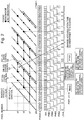
- Fig. 8 is a schematic configuration diagram of a linear CMOS image sensor in which the technique described in Patent Literature 1 is applied
- Fig. 9 is a model diagram for explaining the method for controlling the charge accumulation time in the configuration shown in Fig. 8 .
- each of a large number of pixels 1 (in the present example, 1024 pieces) horizontally arranged in a row includes: one photodiode 11; one readout switch 12 for connecting the photodiode 11 and the common signal output line 2; and one discharge switch 13 for connecting the photodiode 11 and a common discharge line 3.
- the readout switch 12 in each pixel 1 is turned on and off by a signal supplied from a readout shift register 8, while the discharge switch 13 is turned on and off by a signal supplied from a discharge shift register 9.
- the internal configuration of the individual pixels 1 is shown in a simplified form, which can actually have a configuration similar to Fig. 7A or 7B .
- Each of the readout and discharge shift registers 8 and 9 consists of serially connected flip flops forming the same number of stages as the pixels. Each of these resisters produces a signal value for sequentially turning on the switches 12 or 13 of the pixels based on an independent start signal and a common clock signal.
- the horizontal axis represents time and the vertical axis represents the serial number (pixel number) assigned to the 1024 pixels.
- the upward-inclined solid lines P indicate the pixel designated by the readout shift register 8 as the target of the readout operation.
- the upward-inclined chain lines Q in the figure indicate the pixel designated by the discharge shift register 9 as the target of the discharging operation.
- the signal-readout operation through the readout switch 12 is performed at the points in time indicated by the white circles on the solid lines P, while the discharging operation through the discharge switch 13 is performed at the points in time indicated by the filled circles on the chain lines Q.
- the time interval between any two white circles horizontally adjacent to each other corresponds to the readout period T, with a filled circle in between.
- the charges accumulated in the pixel are entirely drained and the charge accumulation once more begins from the reset state.
- the effective charge accumulation time at this pixel is the interval of time between the filled circle and the white circle on the right side, Tc, which is shorter than T.
- Tc is equal to the operation delay time d of the two shift registers 8 and 9. This operation delay time d is determined by the two start signals respectively given to the two shift registers 8 and 9.
- the amount of charges produced in the photodiode in each pixel of the linear image sensor should preferably be as high as possible within a range that does not exceed the signal saturation level.
- many light sources used in spectrometry such as the deuterium lamp, emit strong bright lines at specific wavelengths. When such light is dispersed into wavelengths and detected with a linear image sensor, one or a small number of pixels which receive a bright line will be illuminated with extremely stronger light than the other pixels. Therefore, to obtain high amounts of charges that ensure adequately high SN ratios at both the pixels which receive bright lines and the other pixels, it is necessary to set an extremely short charge accumulation time for specific pixels which receive bright lines and to set an adequately long charge accumulation time for the other pixels.
- Patent Literature 2 discloses a method in which the operation of reading a signal from each pixel is not always performed at specified intervals of time; instead, the function of determining, for each pixel, whether or not the readout operation should be omitted at that pixel is provided so that the charge accumulation time at any specific pixel can be increased to an integer multiple of the readout period by appropriately omitting the readout operation at that specific pixel.
- this method allows the setting of a charge accumulation time longer than the readout period at an arbitrary pixel, it does not allow the opposite, i.e. the setting of a charge accumulation time shorter than the readout period at an arbitrary pixel.
- the conventional techniques may possibly allow some pixels to inevitably reach signal saturation or prevent other pixels from accumulating a necessary amount of charges for obtaining an adequate SN ratio.
- the present invention has been developed in view of such a problem, and its objective is to provide a linear image sensor and its driving method in which the light signal generated in any pixel can be prevented from saturation, and in which the amount of signal close to the saturation level can be obtained at any pixel which receives low-intensity light, even in the case where the wavelength-intensity distribution of the light source includes a bright line or similar wavelength at which the light intensity is extremely high as compared to the other wavelength regions.
- a linear image sensor according to the present invention aimed at solving the previously described problem includes:
- the drive controller commands the turning on/off of the readout switch and the discharge switch of each pixel in such a manner that, within a predetermined readout period, the readout switches in the N pixels are sequentially turned on, once for each pixel, while the discharge switches in at least some of the pixels are temporarily turned on in a predetermined order.
- the photoelectric conversion element is normally a photodiode.
- the signal-generating section may consist of only a photodiode, or it may additionally include a floating diffusion for converting the amount of charges into a voltage signal, a transfer gate for transferring the accumulated charges from the photodiode to the floating diffusion, and other components.
- the signal output line is a line for serially reading charge signals or voltage signals from the pixels and is common to all the pixels, while the discharge line is a line for removing unnecessary charges to the outside of a semiconductor substrate or other areas and does not need to be common to all the pixels.
- the drive controller typically outputs command values to turn on the readout switches of all the pixels sequentially and at predetermined intervals of time.
- the charge or voltage signal is read from each pixel through the readout switch to the output signal line, once for each pixel, within a predetermined readout period T. If the discharge switches were not turned on at all, every pixel would have the same charge accumulation time.
- the drive controller in the present invention issues commands to turn on the discharge switch in any one or more pixels among the entire group of pixels.
- the period of time from a point when the readout switch was turned off in one pixel to the next point when the same readout switch is turned off is the charge accumulation period for accumulating photocharges generated in the photoelectric conversion element by incident light. If the discharge switch is turned on in the middle of this period, the charges accumulated until that point are entirely drained, so that the charge accumulation period is effectively reduced. Accordingly, the specific pixel in which the discharge switch has been turned on has a shorter charge accumulation time than a pixel in which the discharge switch has not been turned on. Therefore, for example, the accumulated charges in that specific pixel are less likely to reach the saturation level even if the light intensity is high.
- the length of the effective charge accumulation period in the pixel concerned depends on the time delay from the point in time where the readout switch is turned off after a predetermined length of time is elapsed from its turning on, to the point in time where the discharge switch is turned off after a predetermined length of time is elapsed from its turning on.
- the command to turn on the readout switch is also issued for each pixel. Therefore, similarly to Patent Literature 2, it is possible to additionally perform a control for increasing the readout operation at any specific pixel by appropriately omitting the readout operation at that pixel. This effectively eliminates the upper limit of the length of the charge accumulation period and provides higher degrees of freedom for setting the charge accumulation period.
- the drive controller may have a configuration including: at least one address scan circuit for selecting each pixel or the readout switch and the discharge switch in each pixel; and N logical gate circuits provided for the N pixels, respectively, with each logical gate circuit allowing or preventing the passage of a command value from the address scan circuit according to an enable signal.
- the address scan circuit can be realized using a shift register.
- the use of a shift register ensures that the pixels will be sequentially selected, and it also reduces the circuit scale.
- a shift register is used as the address scan circuit, either a configuration having an increased number of stages instead of an increased number of shift registers (serial configuration) or a configuration having an increased number of shift registers instead of an increased number of stages per one shift register (parallel configuration) can be adopted to output a plurality of command values for adjusting the charge accumulation period for each pixel.
- the valid value of the enable signal is also a high-level voltage value corresponding to the logical "1”
- both the first and second gate circuits can be an AND gate circuit.
- a preferable method for driving the linear image sensor according to the first mode includes:
- one of the M start signals is used to perform a scan for sequentially turning on the readout switches of the pixels, while the other M-1 start signals are used to perform a scan for sequentially turning on the discharge switches of the pixels.
- the command value outputted from a phase identification circuit assigned to a pixel has become the command value for turning on the readout or discharge switch, whether or not the switch actually turns on depends on the level of the enable signal. Accordingly, it is possible to turn on the discharge switch of any pixel with a timing corresponding to the delay time of the start signal during the readout period T. This enables the actual charge accumulation time to be shorter than the charge accumulation time approximately equal to the readout period T by an amount corresponding to the delay time. For example, if M has a value of 4, there are three possible choices of the delay time for the removal of electric charges and hence three possible choices of the charge accumulation time shorter than the readout period T.
- the valid value of the enable signal is also a high-level voltage value corresponding to the logical "1”
- all the M gate circuits may be an AND gate.
- a preferable method for driving the linear image sensor according to the second mode includes:
- This mode of operation will be similar to the first mode if the M start signals which are inputted into one shift register during the readout period T in the first mode are respectively inputted into the M shift registers, with one signal for each shift register.
- the second mode requires more complex wiring than the first mode but allows the use of a clock signal with a shorter period.
- the linear image sensor and its driving method according to the present invention it is possible to dramatically shorten the charge accumulation time in an arbitrary number of pixels located at arbitrary positions among the entire group of N pixels as compared to the other pixels. Therefore, when the linear image sensor according to the present invention is used as a detector for a spectrometric device, even if the wavelength-intensity distribution of the light source includes a bright line or similar wavelength at which the light intensity is extremely high as compared to the other wavelength regions, it is possible to prevent one or more pixels receiving the bright line from being saturated with photocharges, while ensuring an adequately long charge accumulation time at any pixel receiving low-intensity light so that the amount of accumulated signals will be close to the saturation level. As a result, high SN ratios can assuredly be achieved at all the pixels without causing signal saturation.
- the linear image sensor of the first embodiment (and that of the second embodiment, which will be described later) is suitable as a detector for a spectrophotometer as shown in Fig. 4 .
- Measurement light emitted from the bright point in a light source 100 having a specific emission spectrum e.g. a deuterium lamp, tungsten lamp or xenon lamp
- a lens 101 is focused by a lens 101 and cast into a sample cell 103 made of quartz glass or a similar transparent material with a liquid sample 104 held inside.
- the transmitted light is focused by a lens 105 and falls onto a light-dispersing device 107 (e.g. a diffraction grating) through a slit 106.
- the transmitted light is dispersed into wavelengths in a one-dimensional direction by the light-dispersing device 107.
- the wavelength-dispersed light S reaches the linear image sensor 108.
- each of the pixels forming the linear image sensor 108 receives a fixed wavelength range of the wavelength-dispersed light S within a fixed range of incident angle.
- the wavelength range of the light falling onto the linear image sensor 108 is approximately 200 nm to 1100 nm.
- Each pixel of the linear image sensor 108 produces a detection signal corresponding to the intensity (amount) of the incident light.
- a blank measurement with no incident light can be performed by blocking the measurement light by closing a shutter 102 located between the lens 101 and the sample cell 103.
- a lens, mirror or similar optical element having such an image-forming function may be provided separately from the light-dispersing element 107.
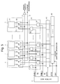
- Fig. 1 is a configuration diagram showing the main components of the linear image sensor according to the first embodiment
- Fig. 2 is a model diagram illustrating a driving method for controlling the charge accumulation time in the linear image sensor of the first embodiment
- Fig. 3 is a sectional view showing a schematic structure of one pixel in the linear image sensor of the first embodiment.
- the pixel structure shown in Fig. 3 is an example of the charge-readout type and is the simplest configuration which has no transfer gate T.
- the logical readout switch is identical to the selection switch X, and the discharge switch is identical to the reset switch R.
- the linear image sensor of the first embodiment consists of N pieces (in the present example, 1024 pieces) of pixels 1 arrayed in a one-dimensional direction, with each pixel including one photodiode 11.
- each pixel 1 includes one readout switch 12 located between the photodiode 11 and a signal output line 2 which is common to all the pixels, and a discharge switch 13 located between the photodiode 11 and a discharge line 3 which is also common to all the pixels.
- Both the readout switch 12 and the discharge switch 13 consist of a MOSFET, which turns on or off the connection between the photodiode 11 and a line (signal output line 2 or discharge line 3) according to the amount of voltage applied to its gate electrode.
- the controller 7 may be integrated with the linear image sensor on the same semiconductor substrate, or it may be provided separately from the sensor.
- the shift register 4 has four-stage flip flops 4a, 4b, 4c and 4d serially connected as one set, with one set of flip flops 4a-4d assigned to each pixel 1.
- the flip flop 4a outputs a command signal for turning on the readout switch 12 or discharge switch 13 in each pixel 1 for a preset period of time, sequentially from the leftmost pixel 1, based on the start signal STR and the clock signal CLK fed from the controller 7.
- One logical gate circuit 5 includes two AND gates 51 and 52, two AND gates 54 and 55 forming a phase identification circuit 110, as well as one three-input OR gate 53.
- the two AND gates 51 and 52 each have one input terminal connected to a common enable signal line 6 through which an enable signal ENBL is supplied from the controller 7.
- the first AND gate 51 which supplies a drive signal to the readout switch 12, has the other input terminal connected to the output of the first-stage flip flop 4a in one set of the shift register 4 via the AND gate 54.
- the second AND gate 52 which supplies a drive signal to the discharge switch 13, has the other input terminal is connected to the output of the flip flop 4a via the AND gate 55.
- a signal line 111a for supplying a phase identification signal PHS1 is connected to the other input terminal of the AND gate 54 which is not connected to any flip flop, while three signal lines 111b, 111c and 111d for respectively supplying phase identification signals PHS2, PHS3 and PHS4 via the output terminal of the three-input OR gate 53 are connected to the other input terminal of the AND gate 53.
- phase #1 is assigned for the scan of the readout switch 12 while the other three phases are assigned for the scan of the discharge switch 13.
- the switch 12 or 13 is in the ON state when the drive signal is at a high-level voltage value (logical "1") and in the OFF state when the drive signal at a low-level voltage value (logical "0").
- these configurations do not constitute limiting factors.
- the clock signal CLK is a pulse signal with a fixed period as shown in Fig. 2 (which will be described later).
- the shift register 4 shifts the signal (logical "1" or "0") held in a flip flop in the previous stage (e.g. 4a) to the flip flop in the next stage (e.g. 4b).
- phase identification signals PHS1-PHS4 as shown in Fig. 2 are generated by the controller 7. Accordingly, four timings for controlling the state of the flip flop 4a are realized in each pixel as the phase changes from #1 through #4.
- the four phases labelled as #1-#4 are respectively assigned to the timings of the readout control, first discharge control, second discharge control and third discharge control (which will be described later).
- the operation of selecting one pixel after another and reading a signal from each pixel is achieved by inputting a start signal into the shift register synchronously with the readout period T.
- the start signal STR is inputted four times into the shift register 4 at different timings during the scan process by the shift register 4 in order to drain electric charges in the middle of the readout period T.
- the first start signal is inputted synchronously with phase #1, indicating the start point of the readout control.
- the next start signal is inputted synchronously with phase #2 after a fixed amount of delay time is elapsed from the aforementioned start signal for the readout control, indicating the start point of the first discharge control.
- the two subsequent start signals are respectively inputted synchronously with phases #3 and #4, indicating the start points of the second and third discharge controls.
- the start signal STR is inputted into the shift register 4, the output of the first-stage flip flop (the leftmost one in Fig. 1 ) is set to the logical "1", i.e. the command value for turning on the switches 12 and 13.
- the value thus set in response to the start signal is shifted to the subsequent flip flop at every single clock of the clock signal CLK.
- the logical gate circuit 5 limits the ON state of the readout switch 12 and the discharge switch 13 of each pixel 1 by allowing or blocking each output value of the phase identification circuits 110 according to the enable signal ENBL. That is to say, when a signal value for turning on the switches 12 and 13 is outputted from the phase identification circuit 110, if the enable signal ENBL is simultaneously set to the high-level voltage value, the output value of the shift register 4 is directly transmitted to the switches 12 and 13, causing these switches 12 and 13 to turn on. Otherwise, i.e. if the enable signal ENBL is at the low-level voltage value, the output value of the shift register 4 does not reach the pixel 1 and the switches 12 and 13 remain in the OFF state.
- the photodiode 11 When the logical "1" outputted from the phase identification circuit 110 reaches the readout switch 12 as a result of setting the enable signal ENBL to the high level, the photodiode 11 is connected to the signal output line 2, so that the signal charges accumulated until that point are entirely read to the signal output line 2. On the other hand, when the logical "1" outputted from the shift register 4 reaches the discharge switch 13 as a result of setting the enable signal ENBL to the high level, the photodiode 11 is connected to the discharge line 3, so that the electric charges accumulated until that point are entirely drained through the discharge line 3 to the outside.
- the reason for using phases #2-#4 for controlling the discharge switch 13 in the present embodiment is to allow the setting of three different lengths of charge accumulation times shorter than the readout time T in addition to the default value of the charge accumulation time which is equal to the readout period T, so as to optimize the charge accumulation time for each pixel 1 so that every pixel will produce approximately the same amount of electric charges. Accordingly, if it is necessary to provide only one choice of the charge accumulation time shorter than the readout period T, only one phase needs to be allotted for the control of the discharge switch 13. In this case, only two phases inclusive of the readout control need to be provided, so that only two stages of flip flops need to be provided per pixel.
- Fig. 2 is an operation timing chart which shows, for ease of explanation, a simplified case where the number N of pixels is four (each pixel 1 having a pixel number of p0, p1, p2 or p3).
- a start signal for the second discharge control as indicated by Q2 is given.
- a start signal for the third discharge control as indicated by Q3 is given.
- the length of time required for the shift register 4 to make a round of scanning all the pixels i.e. the readout period T, is equal to the interval of the points in time at which the readout switch 12 is turned on; this length corresponds to 16 clocks of the clock signal CLK.
- the readout period T corresponds to the maximum value of the charge accumulation time.
- the charge accumulation time in a pixel will be the maximum if the discharge switch 13 in that pixel is not turned on within the period of time from the point where the readout switch 12 of that pixel is turned on to read the charge signal and then turned off, to the point where the same readout switch 12 is turned on the next time (i.e. after one round of scanning the pixels is completed) to read the charge signal.
- the signal charges accumulated until that point are extracted to the signal output line 2 and sent through this line 2 to the outside. Simultaneously with the readout of the signal charges, the potential of the photodiode 11 in the pixel p3 is reset, after which the accumulation of the electric charges produced by photoelectric conversion from the incident light is immediately resumed.
- phase #2 which is five clocks later than the previously described signal-readout operation
- a command value of logical "1" for turning on the discharge switch 13 at the timing which accords with the first discharge control (line Q1 in Fig. 2 ) is fed from the phase identification circuit 110 to the logical gate circuit 5 assigned to the pixel p3.
- this command value is blocked by the AND gate 52 and cannot reach the pixel p3, since the enable signal ENBL at this point is maintained at the low level. Accordingly, the charge accumulation in the photodiode 11 of the pixel p3 is continued.
- phase #3 which is 10 clocks later than the previously described signal-readout operation
- a command value of logical "1" for turning on the discharge switch 13 at the timing which accords with the second discharge control (line Q2 in Fig. 2 ) is fed from the phase identification circuit 110 to the logical gate circuit 5 assigned to the pixel p3.
- the command value passes through the AND gate 52 and reaches the pixel p3.
- the discharge switch 13 of the pixel p3 is turned on, causing the electric charges accumulated in the photodiode 11 until that point to be entirely drained through the discharge line 3 to the outside.
- the potential of the photodiode 11 is once more reset.
- the discharge switch 13 is turned off once more, the charge accumulation in the photodiode 11 of the pixel p3 is resumed from the reset state.
- phase #4 which is 15 clocks later than the previously described signal-readout operation, a command value of logical "1" for turning on the discharge switch 13 at the timing which accords with the third discharge control (line Q3 in Fig. 2 ) is fed from the phase identification circuit 110 to the logical gate circuit 5 assigned to the pixel p3.
- this command value is blocked by the AND gate 52 and cannot reach the pixel p3, since the enable signal ENBL is maintained at the low level. Accordingly, the charge accumulation in the photodiode 11 of the pixel p3 is continued.
- the readout switch 12 is once more turned on to read signal charges accumulated in the photodiode 11 of the pixel p3.
- the amount of signal charges read this time is the result of the accumulation which began at the intermediate point when the previously accumulated electric charges were entirely drained at phase #3.
- the charge accumulation time corresponds to 6 clocks.
- the discharging operation is not performed at any timing for the two pixels p0 and p1. Therefore, the charge accumulation time for these two pixels has a length corresponding to 16 clocks, which is equal to the readout period T.
- the discharging operation is performed at the timing of phase #2 according to the first discharge control, and therefore, the charge accumulation time has a length corresponding to 11 clocks.
- the charge accumulation time in addition to the maximum value, i.e. the readout period T. The choice of which pixel should be given which of the possible values of the charge accumulation time, can be made through the timing of switching the enable signal ENBL to the high level.
- the linear image sensor of the present embodiment it is possible to set a charge accumulation time shorter than the readout period T in an arbitrary number of pixels located at arbitrary positions.
- the positions on the linear image sensor 108 of the pixels which receive a bright line having an extremely high level of intensity among the components of light emitted from the light source 100 are fixed. Therefore, for example, it is possible to set an extremely short charge accumulation time at those pixels to prevent them from being saturated with electric charges.
- a signal with an adequately high SN ratio can be obtained at every pixel (or at every wavelength), while preventing the pixel from being saturated with electric charges, by previously investigating the intensity of light received by each pixel without passing through the liquid sample 104 and then finely adjusting the charge accumulation time at each pixel according to the intensity distribution.
- FIG. 5 is a configuration diagram showing the main components of the linear image sensor according to the second embodiment
- Fig. 6 is a model diagram illustrating the driving method for controlling the charge accumulation time in the linear image sensor of the second embodiment.
- the components identical or corresponding to those of the first embodiment are denoted by the same numerals.
- the linear image sensor of the second embodiment is completely identical to that of the first embodiment in terms of the configuration of each individual pixel 1. A difference exists in that the number of shift registers is increased in exchange for the decreased number of stages of each shift register. It should be noted that the second embodiment is configured to realize only one choice of the charge accumulation time that is shorter than the readout period T. To this end, there are two N-stage shift registers (41 and 42). The first shift register 41 is used to scan the readout switches 12, while the second shift register 42 is used to scan the discharge switches 13. The clock signal CLK supplied from the controller 7 is common to both shift registers 41 and 42, whereas the start signals STR1 and STR2 are independent from each other. The enable signal is also separated into two, one for the readout control and the other for the discharge control.
- the operation for controlling the charge accumulation time is also approximately the same as in the first embodiment: After the start signal STR1 for the readout control is inputted into the first shift register 41, the start signal STR2 for the discharge control is inputted into the second shift register 42 with a predetermined amount of delay time. This delay in time determines the length of the charge accumulation time shorter than the readout period T. As shown in Fig.
- the charge accumulation time at an arbitrary pixel can also be increased to k times the readout period T (where k is an integer equal to or greater than two) by appropriately omitting the readout operation performed according to the readout period T.
- the charge accumulation time at the pixel q is increased to two times the readout period T by omitting the readout operation one time by maintaining the enable signal ENBL1 at the low level at a timing when a command value of logical "1" for turning on the switch 12 is present at the output of the flip flop assigned to the pixel q in the first shift register 4a.
- the charge accumulation time cannot only be shorter than the readout period T but also longer than this period. This also holds true in the first embodiment.
- the linear image sensor it is possible to allot an optimum or nearly optimum charge accumulation time to any of the pixels forming the linear CMOS image sensor, by combining a shift register having [number of pixels] ⁇ [number of phases necessary for control] stages with logical gate circuits, or by combining [number of phases necessary for control] shift registers each having [number of pixels] stages with logical gate circuits.
- the number of phases necessary for control in the present context is the sum of the number of readout controls and that of the discharge controls. This number is "four" in the first embodiment and "two" in the second embodiment.
Landscapes
- Engineering & Computer Science (AREA)
- Multimedia (AREA)
- Signal Processing (AREA)
- Transforming Light Signals Into Electric Signals (AREA)
- Facsimile Heads (AREA)
- Solid State Image Pick-Up Elements (AREA)
Applications Claiming Priority (2)
| Application Number | Priority Date | Filing Date | Title |
|---|---|---|---|
| JP2012238850 | 2012-10-30 | ||
| PCT/JP2013/079111 WO2014069394A1 (fr) | 2012-10-30 | 2013-10-28 | Capteur d'image linéaire et procédé de pilotage associé |
Publications (2)
| Publication Number | Publication Date |
|---|---|
| EP2911384A1 true EP2911384A1 (fr) | 2015-08-26 |
| EP2911384A4 EP2911384A4 (fr) | 2015-11-04 |
Family
ID=50627300
Family Applications (1)
| Application Number | Title | Priority Date | Filing Date |
|---|---|---|---|
| EP13851721.4A Withdrawn EP2911384A4 (fr) | 2012-10-30 | 2013-10-28 | Capteur d'image linéaire et procédé de pilotage associé |
Country Status (4)
| Country | Link |
|---|---|
| US (1) | US20150296160A1 (fr) |
| EP (1) | EP2911384A4 (fr) |
| JP (1) | JPWO2014069394A1 (fr) |
| WO (1) | WO2014069394A1 (fr) |
Families Citing this family (5)
| Publication number | Priority date | Publication date | Assignee | Title |
|---|---|---|---|---|
| US9508765B2 (en) * | 2014-09-02 | 2016-11-29 | Shimadzu Corporation | Photodiode array detector with different charge accumulation time for each light receiving element within one unit |
| JP7048448B2 (ja) * | 2018-08-14 | 2022-04-05 | 株式会社東芝 | 固体撮像装置 |
| JP6824363B1 (ja) | 2019-10-30 | 2021-02-03 | 浜松ホトニクス株式会社 | イメージセンサ、及びイメージセンサの制御方法 |
| CN116132831B (zh) * | 2023-01-06 | 2026-03-03 | 威海华菱光电股份有限公司 | 线阵图像传感器芯片和图像传感器 |
| SE2450327A1 (en) * | 2024-03-25 | 2025-09-26 | Spec Imaging Ab | An assembly for measurements of one or more optical parameters of a sample medium and a method for measuring one or more optical parameters of a sample medium using an assembly |
Family Cites Families (23)
| Publication number | Priority date | Publication date | Assignee | Title |
|---|---|---|---|---|
| JPS6111622A (ja) * | 1984-06-27 | 1986-01-20 | Hitachi Ltd | 分光光度計 |
| ES2038255T3 (es) * | 1988-08-17 | 1993-07-16 | Hewlett-Packard Gmbh | Espectrometro con un conjunto ordenado de fotodiodos. |
| JP3166776B2 (ja) * | 1990-11-30 | 2001-05-14 | キヤノン株式会社 | 撮像装置及び撮像方法 |
| JP3013584B2 (ja) | 1992-02-14 | 2000-02-28 | ソニー株式会社 | 固体撮像装置 |
| JPH0815013A (ja) * | 1994-06-29 | 1996-01-19 | Shimadzu Corp | 分光光度計 |
| US6097021A (en) * | 1997-01-06 | 2000-08-01 | Texas Instruments Incorporated | Apparatus and method for a managed integration optical sensor array |
| JP4365912B2 (ja) * | 1998-11-18 | 2009-11-18 | キヤノン株式会社 | 撮像装置及びそれを用いた撮像システム |
| US6657662B1 (en) * | 1999-09-03 | 2003-12-02 | Xerox Corporation | System for resetting the video offset from dark photosensors in an image sensor array |
| TW530480B (en) * | 2001-09-27 | 2003-05-01 | Microtek Int Inc | Image sensor device and control method of scanner using the same |
| US7408683B2 (en) * | 2002-07-15 | 2008-08-05 | Brother Kogyo Kabushiki Kaisha | Image sensor for reading image and image reading apparatus including the image sensor |
| JP4325557B2 (ja) * | 2005-01-04 | 2009-09-02 | ソニー株式会社 | 撮像装置および撮像方法 |
| JP5197915B2 (ja) * | 2005-06-20 | 2013-05-15 | 浜松ホトニクス株式会社 | イメージセンサ |
| JP4745851B2 (ja) * | 2006-02-09 | 2011-08-10 | キヤノン株式会社 | 撮像装置 |
| US7427736B2 (en) * | 2006-03-23 | 2008-09-23 | Micron Technology, Inc. | Method and apparatus for providing a rolling double reset timing for global storage in image sensors |
| JP4208904B2 (ja) * | 2006-07-03 | 2009-01-14 | キヤノン株式会社 | 撮像装置及びその制御方法並びに撮像システム |
| JP4789767B2 (ja) * | 2006-09-28 | 2011-10-12 | キヤノン株式会社 | 撮像装置及びその制御方法 |
| JP5172267B2 (ja) * | 2007-10-09 | 2013-03-27 | 富士フイルム株式会社 | 撮像装置 |
| JP5225145B2 (ja) * | 2009-02-23 | 2013-07-03 | キヤノン株式会社 | 固体撮像装置 |
| FR2961019B1 (fr) * | 2010-06-03 | 2013-04-12 | Commissariat Energie Atomique | Capteur d'image lineaire en technologie cmos |
| JP2012129799A (ja) * | 2010-12-15 | 2012-07-05 | Sony Corp | 固体撮像素子および駆動方法、並びに電子機器 |
| JP2012182657A (ja) * | 2011-03-01 | 2012-09-20 | Sony Corp | 撮像装置、および撮像装置制御方法、並びにプログラム |
| JP2013005017A (ja) * | 2011-06-13 | 2013-01-07 | Sony Corp | 撮像装置、および撮像装置制御方法、並びにプログラム |
| JP6146015B2 (ja) * | 2013-01-18 | 2017-06-14 | 株式会社リコー | 光電変換素子、画像読取装置及び画像形成装置 |
-
2013
- 2013-10-28 WO PCT/JP2013/079111 patent/WO2014069394A1/fr not_active Ceased
- 2013-10-28 JP JP2014544490A patent/JPWO2014069394A1/ja active Pending
- 2013-10-28 US US14/438,260 patent/US20150296160A1/en not_active Abandoned
- 2013-10-28 EP EP13851721.4A patent/EP2911384A4/fr not_active Withdrawn
Also Published As
| Publication number | Publication date |
|---|---|
| EP2911384A4 (fr) | 2015-11-04 |
| JPWO2014069394A1 (ja) | 2016-09-08 |
| US20150296160A1 (en) | 2015-10-15 |
| WO2014069394A1 (fr) | 2014-05-08 |
Similar Documents
| Publication | Publication Date | Title |
|---|---|---|
| EP2911384A1 (fr) | Capteur d'image linéaire et procédé de pilotage associé | |
| US7649618B2 (en) | System and method to perform raman imaging without luminescence | |
| US7342212B2 (en) | Analog vertical sub-sampling in an active pixel sensor (APS) image sensor | |
| US6731335B1 (en) | CMOS image sensor having common outputting transistors and method for driving the same | |
| EP3101812B1 (fr) | Amplificateur de transconductance différentielle intrapixel pour can et architecture de capteur d'image | |
| KR100979197B1 (ko) | 고체촬상장치 | |
| US9666618B2 (en) | Pixel array with individual exposure control using at least two transfer gates for a pixel or pixel region | |
| EP2517461B1 (fr) | Circuits de sortie de colonne pour capteurs d'image | |
| US20110205384A1 (en) | Variable active image area image sensor | |
| EP0355174B1 (fr) | Spectromètre à réseau de photodiodes | |
| EP4395359A1 (fr) | Élément d'imagerie et dispositif d'imagerie | |
| US20220375214A1 (en) | High resolution fast framing infrared detection system | |
| EP2461575A1 (fr) | Dispositif de prise d image à semi-conducteurs | |
| EP1757912B1 (fr) | Appareil photo-détecteur | |
| US20130063640A1 (en) | Solid-state imaging device | |
| US7256379B2 (en) | Optical sensing device | |
| JP2017175107A (ja) | 撮像装置 | |
| EP1736751B1 (fr) | Capteur d'images | |
| EP1874044B1 (fr) | Dispositif d'imagerie a semi-conducteur | |
| Eminoglu et al. | MT6425CA: a 640 x 512-25µm CTIA ROIC for SWIR InGaAs detector arrays | |
| CN113709391B (zh) | Cmos图像传感器及其读取方法 | |
| US7683952B2 (en) | Optical image information detecting apparatus | |
| JPH04268422A (ja) | 分光装置 | |
| JP2004328730A (ja) | センサアレイを制御する方法及び装置 | |
| WO2025248972A1 (fr) | Dispositif de mesure spectroscopique et procédé de mesure spectroscopique |
Legal Events
| Date | Code | Title | Description |
|---|---|---|---|
| PUAI | Public reference made under article 153(3) epc to a published international application that has entered the european phase |
Free format text: ORIGINAL CODE: 0009012 |
|
| 17P | Request for examination filed |
Effective date: 20150522 |
|
| AK | Designated contracting states |
Kind code of ref document: A1 Designated state(s): AL AT BE BG CH CY CZ DE DK EE ES FI FR GB GR HR HU IE IS IT LI LT LU LV MC MK MT NL NO PL PT RO RS SE SI SK SM TR |
|
| AX | Request for extension of the european patent |
Extension state: BA ME |
|
| RA4 | Supplementary search report drawn up and despatched (corrected) |
Effective date: 20151007 |
|
| RIC1 | Information provided on ipc code assigned before grant |
Ipc: H01L 27/146 20060101ALI20151001BHEP Ipc: H04N 5/369 20110101AFI20151001BHEP Ipc: H04N 5/374 20110101ALI20151001BHEP |
|
| DAX | Request for extension of the european patent (deleted) | ||
| STAA | Information on the status of an ep patent application or granted ep patent |
Free format text: STATUS: THE APPLICATION HAS BEEN WITHDRAWN |
|
| 18W | Application withdrawn |
Effective date: 20190206 |