EP2911405A1 - Elektronische vorrichtung, ladungssteuerungsverfahren für die elektronische vorrichtung, verfahren zur anzeige der verbleibenden batterieladung der elektronischen vorrichtung, quellvorrichtung und senkenvorrichtung - Google Patents
Elektronische vorrichtung, ladungssteuerungsverfahren für die elektronische vorrichtung, verfahren zur anzeige der verbleibenden batterieladung der elektronischen vorrichtung, quellvorrichtung und senkenvorrichtung Download PDFInfo
- Publication number
- EP2911405A1 EP2911405A1 EP13847566.0A EP13847566A EP2911405A1 EP 2911405 A1 EP2911405 A1 EP 2911405A1 EP 13847566 A EP13847566 A EP 13847566A EP 2911405 A1 EP2911405 A1 EP 2911405A1
- Authority
- EP
- European Patent Office
- Prior art keywords
- unit
- line
- external device
- mhl
- charging
- Prior art date
- Legal status (The legal status is an assumption and is not a legal conclusion. Google has not performed a legal analysis and makes no representation as to the accuracy of the status listed.)
- Granted
Links
Images






Classifications
-
- H—ELECTRICITY
- H04—ELECTRIC COMMUNICATION TECHNIQUE
- H04N—PICTORIAL COMMUNICATION, e.g. TELEVISION
- H04N21/00—Selective content distribution, e.g. interactive television or video on demand [VOD]
- H04N21/40—Client devices specifically adapted for the reception of or interaction with content, e.g. set-top-box [STB]; Operations thereof
- H04N21/43—Processing of content or additional data, e.g. demultiplexing additional data from a digital video stream; Elementary client operations, e.g. monitoring of home network or synchronising decoder's clock; Client middleware
- H04N21/443—OS processes, e.g. booting an STB, implementing a Java virtual machine in an STB or power management in an STB
- H04N21/4436—Power management, e.g. shutting down unused components of the receiver
-
- H—ELECTRICITY
- H04—ELECTRIC COMMUNICATION TECHNIQUE
- H04N—PICTORIAL COMMUNICATION, e.g. TELEVISION
- H04N21/00—Selective content distribution, e.g. interactive television or video on demand [VOD]
- H04N21/40—Client devices specifically adapted for the reception of or interaction with content, e.g. set-top-box [STB]; Operations thereof
- H04N21/41—Structure of client; Structure of client peripherals
- H04N21/426—Internal components of the client ; Characteristics thereof
-
- H—ELECTRICITY
- H04—ELECTRIC COMMUNICATION TECHNIQUE
- H04N—PICTORIAL COMMUNICATION, e.g. TELEVISION
- H04N21/00—Selective content distribution, e.g. interactive television or video on demand [VOD]
- H04N21/40—Client devices specifically adapted for the reception of or interaction with content, e.g. set-top-box [STB]; Operations thereof
- H04N21/41—Structure of client; Structure of client peripherals
- H04N21/4104—Peripherals receiving signals from specially adapted client devices
- H04N21/4122—Peripherals receiving signals from specially adapted client devices additional display device, e.g. video projector
-
- H—ELECTRICITY
- H04—ELECTRIC COMMUNICATION TECHNIQUE
- H04N—PICTORIAL COMMUNICATION, e.g. TELEVISION
- H04N21/00—Selective content distribution, e.g. interactive television or video on demand [VOD]
- H04N21/40—Client devices specifically adapted for the reception of or interaction with content, e.g. set-top-box [STB]; Operations thereof
- H04N21/41—Structure of client; Structure of client peripherals
- H04N21/414—Specialised client platforms, e.g. receiver in car or embedded in a mobile appliance
- H04N21/41407—Specialised client platforms, e.g. receiver in car or embedded in a mobile appliance embedded in a portable device, e.g. video client on a mobile phone, PDA, laptop
-
- H—ELECTRICITY
- H04—ELECTRIC COMMUNICATION TECHNIQUE
- H04N—PICTORIAL COMMUNICATION, e.g. TELEVISION
- H04N21/00—Selective content distribution, e.g. interactive television or video on demand [VOD]
- H04N21/40—Client devices specifically adapted for the reception of or interaction with content, e.g. set-top-box [STB]; Operations thereof
- H04N21/43—Processing of content or additional data, e.g. demultiplexing additional data from a digital video stream; Elementary client operations, e.g. monitoring of home network or synchronising decoder's clock; Client middleware
- H04N21/436—Interfacing a local distribution network, e.g. communicating with another STB or one or more peripheral devices inside the home
-
- H—ELECTRICITY
- H04—ELECTRIC COMMUNICATION TECHNIQUE
- H04N—PICTORIAL COMMUNICATION, e.g. TELEVISION
- H04N21/00—Selective content distribution, e.g. interactive television or video on demand [VOD]
- H04N21/40—Client devices specifically adapted for the reception of or interaction with content, e.g. set-top-box [STB]; Operations thereof
- H04N21/43—Processing of content or additional data, e.g. demultiplexing additional data from a digital video stream; Elementary client operations, e.g. monitoring of home network or synchronising decoder's clock; Client middleware
- H04N21/436—Interfacing a local distribution network, e.g. communicating with another STB or one or more peripheral devices inside the home
- H04N21/4363—Adapting the video stream to a specific local network, e.g. a Bluetooth® network
- H04N21/43632—Adapting the video stream to a specific local network, e.g. a Bluetooth® network involving a wired protocol, e.g. IEEE 1394
-
- G—PHYSICS
- G06—COMPUTING OR CALCULATING; COUNTING
- G06F—ELECTRIC DIGITAL DATA PROCESSING
- G06F1/00—Details not covered by groups G06F3/00 - G06F13/00 and G06F21/00
- G06F1/26—Power supply means, e.g. regulation thereof
Definitions
- the present invention relates to an electronic device, a charging control method of the electronic device, a battery power-level display method of the electronic device, a source device, and a sink device, and particularly, to an electronic device that transmits content data through a digital interface between external devices, or the like.
- MHL mobile high-definition link
- An object of the present invention is to perform successful communication required between external devices.
- an electronic device including: a content data processing unit that is connected to an external device through a first line; and a communication unit that is connected to the external device through a second line, in which the communication unit transmits an inquiry signal to the external device through the second line in a state in which the first line is unavailable.
- the present technology includes the content data processing unit and the communication unit.
- the content data processing unit is connected to the external device through the first line.
- the communication unit is connected to the external device through the second line.
- the content data processing unit represents, for example, a content data transmitting unit that transmits content data to the external device, or a content data receiving unit that receives the content data from the external device.
- the communication unit transmits the inquiry signal to the external device through the second line in the state in which the first line is unavailable.
- the communication unit may recognize that the first line is in a state of being unavailable based on a resistance value between the second line and a ground line.
- the first line enters the unavailable state and it is not possible to transmit the content data through the first line.
- the inquiry signal is transmitted to the external device through the second line in the state in which the first line is unavailable. Therefore, in the state in which the first line is unavailable, for example, in a case where the interface unit is in a standby state, it is possible to inquire a required item to the external device while the standby state is maintained. In this case, since it is possible to decrease power consumption of the external device as much as possible, it is possible to contribute to saving of energy of the external device.
- the communication unit may receive a response signal in response to the inquiry signal from the external device through the second line in a state in which the first line is unavailable.
- the response signal in response to the inquiry signal may be received from the external device through a line other than the second line. It is considered that a power supply line or the like is used as the line other than the second line.
- the electronic device may further include: a charging unit that is connected to a power supply unit of the external device through a third line; and a charging control unit that controls a charging operation of the charging unit, in which the inquiry signal may indicate a signal generated to inquire current supply capability of the external device, and in which the charging control unit may control a value of a current which is drawn from the third line by the charging unit, in accordance with the response signal.
- the response signal may contain information of an upper limit current value.
- the response signal may contain information representing a type of upper limit current value.
- the interface unit is in the standby state, it is possible to acquire the response signal containing information of the current supply capability from the external device while the standby state is maintained, the current supply capability of the external device is used up to the upper limit for charging, and it is possible to achieve fast charging.
- the electronic device may further include: a power supply unit that is connected to a charging unit of the external device through a third line; a display unit; and a display control unit that controls a display operation of the display unit, in which the inquiry signal may indicate a signal generated to inquire a battery power level of the external device, and in which the display control unit may display battery power level information of the external device on the display unit, in accordance with the response signal.
- the inquiry signal may indicate a signal generated to inquire a battery power level of the external device
- the display control unit may display battery power level information of the external device on the display unit, in accordance with the response signal.
- an electronic device including: a digital interface unit that is connected to a digital interface unit of an external device through a transmission path, in which the digital interface unit includes a content data processing unit that is connected to the digital interface unit of the external device through a first line; and a communication unit that is connected to the digital interface unit of the external device through a second line, in which the communication unit transmits an inquiry signal to the digital interface unit of the external device through the second line when the digital interface unit of the external device is in a standby state.
- the present technology includes the digital interface unit that is connected to the digital interface unit of the external device through the transmission path.
- the digital interface unit includes the content data processing unit and the communication unit.
- the content data processing unit is connected to the external device through the first line.
- the communication unit is connected to the external device through the second line.
- the content data processing unit represents, for example, a content data transmitting unit that transmits content data to the external device, or a content data receiving unit that receives the content data from the external device.
- the communication unit transmits an inquiry signal to the digital interface unit of the external device through the second line when the digital interface unit of the external device is in the standby state.
- the first line enters the unavailable state and it is not possible to transmit the content data through the first line.
- the digital interface may indicate the interface having a mobile high-definition link (MHL) standard.
- the inquiry signal is transmitted to the external device through the second line when the digital interface unit of the external device is in the standby state. Therefore, in a case where the digital interface unit of the external device is in the standby state, it is possible to inquire a required item to the external device while the standby state is maintained. In this case, since it is possible to decrease power consumption of the external device as much as possible, it is possible to contribute to saving of energy of the external device.
- the communication unit may receive a response signal in response to the inquiry signal from the digital interface unit of the external device through the second line when the digital interface unit of the external device is in the standby state.
- the response signal in response to the inquiry signal may be received from the external device through a line other than the second line. It is considered that a power supply line or the like is used as the line other than the second line.
- a source device including: a content data transmitting unit that is connected to a sink device through a first line; a communication unit that is connected to the sink device through a second line; a charging unit that is connected to a power supply unit of the sink device through a third line; and a charging control unit that controls a charging operation of the charging unit, in which, when the first line is in a state of being unavailable, the communication unit transmits an inquiry signal generated to inquire current supply capability of the sink device through the second line and receives a response signal in response to the inquiry signal from the source device; and in which the charging control unit controls a value of a current which is drawn from the third line by the charging unit, in accordance with the response signal.
- a sink device including: a content data receiving unit that is connected to a source device through a first line; a communication unit that is connected to the source device through a second line; a power supply unit that is connected to a charging unit of the source device through a third line; a display unit; and a display control unit that controls a display operation of the display unit, in which, when the first line is in a state of being unavailable, the communication unit transmits an inquiry signal generated to inquire a battery power level of the source device through the second line to the source device and receives a response signal in response to the inquiry signal from the source device; and in which the display control unit displays battery power level information of the external device on the display unit, in accordance with the response signal.
- Fig. 1 illustrates a configuration example of an image display system 10 as an embodiment.
- the image display system 10 is configured to include a mobile phone 100 as a mobile high-definition link (MHL) source device, and a television 200 as an MHL sink device. These devices are connected to each other by an MHL cable 300.
- MHL mobile high-definition link
- the MHL is mainly an audio visual (AV) digital interface standard for a mobile device.
- the MHL causes the MHL source device and the MHL sink device to be connected to each other by an MHL cable and contents such as a video image, a still image, or a sound loaded in the MHL source device are reproduced by the MHL sink device (AV stream in one direction).
- control such as EDID reading, HDCP authentication, register reading/writing, or remote control is performed between the devices by transmitting and receiving a DDC command and an MHL sideband channel (MSC) command (bidirectional link control).
- MSC MHL sideband channel
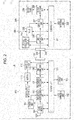
- Fig. 2 illustrates a configuration example of the mobile phone 100 and the television 200 which configure the image display system.
- the mobile phone 100 includes a control unit 101, a user operation unit 102, and a display unit 103.
- the mobile phone 100 includes a 3G/4G modem 104, a camera unit 105, a recording/reproducing unit 106, a transmission processing unit 107, an MHL transmitting unit (MHL source) 108, and an MHL terminal 109.
- the mobile phone 100 includes a charging circuit 110 and a battery 111.
- the control unit 101 controls an operation of each unit of the mobile phone 100.
- the user operation unit 102 and the display unit 103 configure a user interface and are connected to the control unit 101.
- the user operation unit 102 is configured to have a key, a button, or a dial which is disposed on a housing (not illustrated) of the mobile phone 100, a touch panel disposed on the display surface of the display unit 103, or the like.
- the display unit 103 is configured of a liquid crystal display (LCD), an organic electro luminescence (EL), or the like.
- the 3G/4G modem 104 performs mobile phone communication.
- the camera unit 105 performs imaging of a moving image or a still image.
- the recording/reproducing unit 106 drives a recording medium such as an embedded memory (nonvolatile memory) or a memory card and performs recording and reproducing (writing and reading).
- the recording/reproducing unit 106 performs recording and reproducing of a call performed through the modem 104.
- the recording/reproducing unit 106 performs recording and reproducing of image data of a moving image and a still image or audio data which is acquired through the modem 104 and performs recording and reproducing of image data of a moving image and a still image or audio data which is obtained by being imaged by the camera unit (including a microphone) 105. Additionally, the recording/reproducing unit 106 performs a codec process in which the image data of the moving image and the still image which is acquired by being imaged by the camera unit 105 is subjected to data compression.
- a user makes an instruction from the user operation unit 102 and thereby, recording contents in the recording medium in the recording/reproducing unit 106 can be displayed as a contents list.
- the user designates any content on the contents list from the user operation unit 102, data of the designated content from the recording medium in the recording/reproducing unit 106 is reproduced and is transferred to the transmission processing unit 107.
- a case is considered, in which the image data and the audio data acquired by the 3G/4G modem 104 or the image data and the audio data obtained by the camera unit 105 are transmitted in real time.
- the content data is not illustrated in the drawings but is directly transferred to the transmission processing unit 107.
- a case is also considered, in which, after a memory card is inserted into another device and content data is written, the memory card is mounted on the recording/reproducing unit 106 and the content data is transmitted to the transmission processing unit 107.
- the transmission processing unit 107 performs a process on data such as a moving image, a still image, or a sound which is reproduced in the recording/reproducing unit 106 and is transmitted to the television 200 such that the data has an appropriate form. For example, a transmission format and a video format of 3D image data are converted such that the data can be processed in the television 200.
- the MHL transmitting unit 108 configures a digital interface unit.
- the MHL transmitting unit 108 is connected to the MHL terminal 109.
- the MHL transmitting unit 108 transmits the data such as the image or sound processed in the transmission processing unit 107 from the MHL terminal 109 to the television 200 through the MHL cable 300 in one direction by communicating in accordance with the MHL standard.
- the MHL transmitting unit 108 will be described later in detail.
- the charging circuit 110 charges the battery 111.
- the charging circuit 110 is connected to a power supply unit (voltage regulator circuit) of the television 200 through a power supply line (VBUS).
- the charging circuit 110 causes a drawing current determined by the control unit 101 to be drawn from the power supply line and to charge the battery 111.
- the battery 111 supplies power to an internal circuit of the mobile phone 100. A control process of the drawing current in the control unit 101 will be described later in detail.
- the television 200 includes a control unit 201, a user operation unit 202, an MHL terminal 203, and an MHL receiving unit (MHL sink) 204.
- the television 200 includes a tuner 205, an antenna terminal 206, a switching unit 207, a display processing unit 208, a display panel 209, and a voltage regulator circuit 210.
- the control unit 201 controls an operation of each unit of the television 200.
- the user operation unit 202 configures a user interface and is connected to the control unit 201.
- the user operation unit 202 is configured to have a key, a button, or a dial which is disposed on a housing (not illustrated) of the television 200, a remote control, or the like.
- the MHL receiving unit 204 configures the digital interface unit.
- the MHL receiving unit 204 is connected to the MHL terminal 203.
- the MHL receiving unit 204 receives data such as an image or a sound which is transmitted, in one direction, from the MHL transmitting unit 108 of the mobile phone 100 which is connected to the MHL receiving unit through the MHL cable 300, by communicating in accordance with the MHL standard.
- the MHL receiving unit 204 supplies the received image data to the switching unit 207. Additionally, the sound data received by the MHL receiving unit 204 is supplied to a switching unit (not illustrated) for sound data.
- the MHL receiving unit 204 will be described later in detail.
- the tuner 205 receives BS broadcasting, digital terrestrial broadcasting, or the like. A broadcasting signal caught by an antenna (not illustrated) connected to the antenna terminal 206 is supplied to the tuner 205.
- the tuner 205 acquires image data (video signal) and sound data of a predetermined program based on the broadcasting signal.
- the switching unit 207 selectively extracts the image data received by the MHL receiving unit 204 or the image data acquired by the tuner 205.
- the display processing unit 208 performs a process of superimposing a subtitle such as a closed caption, graphics, or the like on the image data extracted by the switching unit 207. In addition, the display processing unit 208 performs a scaling process and an image quality improving process on the image data extracted by the switching unit 207 and then, obtains image data for display.
- the display panel 209 displays an image formed by the image data for display which is obtained by the display processing unit 208.
- the display panel 209 is configured of, for example, a liquid crystal display (LCD), an organic electro luminescence (EL), and a plasma display panel (PDP).
- the voltage regulator circuit 210 configures the power supply unit.
- the voltage regulator circuit 210 supplies power to the television 200.
- the voltage regulator circuit 210 supplies power to the mobile phone 110 through the power supply line.
- Fig. 3 illustrates a configuration example of the MHL transmitting unit 108 of the mobile phone 100 in Fig. 2 and the MHL receiving unit 204 of the television 200.
- the MHL transmitting unit 108 includes a transmitter and the MHL receiving unit 204 includes a receiver.
- the MHL transmitting unit 108 and the MHL receiving unit 204 are connected to each other through pins of five lines (MHL+, MHL-, CBUS, VBUS, and GND) and the MHL cable 300.
- a pin assignment varies depending on a connector.
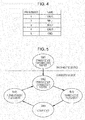
- Fig. 4 illustrates an example of the pin assignment.
- MHL+ and MHL- are a twisted pair and transmits an AV stream and a synchronized signal (MHL clock) thereof.
- CBUS is used to transmit a DDC command and an MSC command in a bidirectional manner.
- the DDC command is used for the EDID reading or the HDCP authentication.
- the MSC command is used to control the EDID reading, read and write of various registers, a remote control, or the like.
- VBUS is used to supply power of +5 V to the MHL source device from the MHL sink device.
- MHL sink MHL sink
- MHL transmitting unit MNL source
- Fig. 5 illustrates a state transition of the sink.
- the sink is in a connection state to the source and has five states as illustrated in the drawing.
- SNK1 represents a state (nonconnection of source) in which the sink is in a standby state (the sink is in a power save mode) and it is not possible to recognize the connection of the source.
- SNK2 represents a state in which the sink is in the standby state (the sink is in a power save mode) and the source is connected.
- SNK3 represents a transitional state in which the sink receives an active request from the source side and a process which is necessary for transition is performed.
- SNK4 represents that the sink is in an active state. Only in this state, the sink can transmit a command through the CBUS. In addition, only in this state, video and audio transmission can be performed through an MHL+/MHL- line from the source to the sink.
- SNK5 represents a transitional state in which the sink returns to the standby state by a request from the source or the sink.
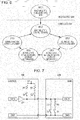
- Fig. 6 illustrates a state transition of the source.
- the source is in a connection state to the sink and has six states as illustrated in the drawing.
- SRC1 represents a state (nonconnection of sink) in which the source is in an inactive state and it is not possible to recognize the connection of the sink.
- SRC2 represents a state in which the source is in the inactive state and is only electrically connected to the sink. At this time, the state of the sink is "SNK2".
- SRC3 represents a transitional state in which the source transmits an active request to the sink side and a process which is necessary for transition is performed.
- the state of the sink is "SNK3".
- SRC4 represents a state in which the source is in an active state, and it is before current supply capability of the sink is acquired, and the current supply capability of the sink is not known.
- the state of the sink is "SNK4".
- SRC5 represents a state in which the source is in an active state and it is after the current supply capability of the sink is acquired.
- the state of the sink is "SNK4".
- the source can transmit a command through the CBUS.
- video and audio transmission that is, content data transmission can be performed through the MHL+/MHL- line from the source to the sink.
- SRC6 represents a transitional state in which the source returns to the inactive state by a request from the source or the sink. At this time, the state of the sink is "SNK5".
- Fig. 7 illustrates a concept of the CBUS when the MHL receiving unit (MHL sink) 204 and the MHL transmitting unit (MHL source) 108 are connected to each other through the MHL cable 300.
- the MHL receiving unit 204 is described as a "SINK”
- the MHL transmitting unit 108 is described as a "SOURCE”.
- the MHL receiving unit 204 has a resistance value between CBUS-GND as R3 (S3 is closed and S4 is opened).
- the sink in a power save mode.
- the sink causes only a standby circuit of an MHL unit to be in an energized state and causes the other circuits of the MHL unit to be in a de-energized state. In the standby circuit, it is possible to detect a voltage change and a pulse width of about tens of milliseconds of the CBUS.
- the source side is pulled up at a voltage V1 and resistance R2 (S1 is opened and S2 is closed). Then, the source monitors the resistance value between CBUS-GND and, when the voltage between CBUS-GND is divided to R2 and R3, the source detects the sink in "SNK2" (standby state) and the source itself is transited to "SRC2". That is, the source recognizes that the sink is in "SNK2" (standby state) based on the resistance value between CBUS-GND. In addition, the source starts to draw a current from the VBUS (not illustrated in Fig. 7 ) with 0.1 A as an upper limit.
- the source When the source issues an active request to the sink, the source transmits a unique pulse illustrated in Fig. 8 , that is, an active request pulse to the sink and transition to "SRC3" is performed to the source on the CBUS.
- a transition direction of the pulse is from the source to the sink.
- a pattern of the pulse which is transmitted is sequentially transmitted from the left direction to the right direction.
- a first half of the pulse width is defined as 20 mS to 60 mS.
- Charging current control in the control unit 101 of the mobile phone 100 is described.
- power of 5 V for battery charging is supplied to the source device from the sink device through the VBUS.
- the maximum possible current drawn by the source varies by the MHL version.
- an MHL version A has 0.5 A
- an MHL version B has 0.9 A or 1.5 A.
- Whether the current supply capability of a certain sink has any one of the cases described above can be determined by reading device capability registers inside the sink.
- the control unit 101 acquires information of the current supply capability of the MHL receiving unit 204 side through the MHL transmitting unit (MHL source) 108 and the charging voltage is determined as follows. Then, the control unit 101 controls the charging circuit 110 such that the determined charging current is drawn from the VBUS.
- the control unit 101 reads the MHL version (registering the MHL version number corresponding to the device itself) in the device capability register and, in a case of the version A, the charging current is determined to be 0.5 A.
- the control unit 101 refers to a device category (register the current supply capability of the device itself). The device category is shown by combining 2-bit values. The control unit 101 determines that "00" corresponds to 0.5 A, "01" corresponds to 0.9 A, and "01" corresponds to 1.5 A.
- a flowchart in Fig. 9 represents an example of a procedure of a determination process of the charging current in the control unit 101.
- the control unit 101 starts a process in Step ST1 and then, proceeds to a process in Step ST2.
- Step ST2 the control unit 101 determines whether or not the MHL version is A and, when the MHL version is A, in Step ST3, the control unit 101 determines that the charging current is 0.5 A and then, in Step ST4, the process ends.
- Step ST2 when the MHL version is not A, that is, when the MHL version is B, the control unit 101 checks the 2-bit value of the device category in Step S5. Then, in Step ST6, the control unit 101 determines whether or not the 2-bit value is "00". When the 2-bit value is "00", in Step ST7, the control unit 101 determines that the charging current is 0.5 A and then, in Step ST4, the process ends.
- Step ST6 the control unit 101 determines whether or not the 2-bit value is "01".
- Step ST9 the control unit 101 determines that the charging current is 0.9 A and then, in Step ST4, the process ends.
- Step ST10 the control unit 101 determines whether or not the 2-bit value is "10".
- Step ST11 the control unit 101 determines that the charging current is 1.5 A and then, in Step ST4, the process ends.
- Step ST12 the control unit 101 determines that an error occurs and immediately, in Step ST4, the process ends.
- the charging current is maintained to be the guaranteed minimum current value of 0.1 A.
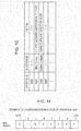
- Fig. 10 illustrates a format (a snippet) of the device capability register.
- the device capability register is configured of a plurality of register spaces including the MHL version, device category, or the like.
- An "offset value" represents a position of the device capability register from the top. For example, the offset value of the MHL version is 0 ⁇ 01, which indicates that the MHL version is positioned at the second byte from the top.
- Fig. 11 illustrates an example of a configuration of the MHL version.
- the example corresponds to an example of a configuration in a case of a version A (0 ⁇ 41).
- Fig. 12 illustrates an example of a configuration of the device category.
- the example corresponds to an example of a configuration in a case of 0.9 A, a bit value of the sixth bit corresponds to "0", and a bit value of the fifth bit corresponds to "1".
- the MHL transmitting unit (MHL source) 108 performs reading of the device capability register using a command defined on the CBUS.
- Fig. 13 illustrates a reading procedure of the MHL version of the MHL receiver (MHL sink) 204 by the MHL transmitter 108 using the command on the CBUS. The reading of the device category is performed in accordance with the procedure.
- the MHL transmitting unit 108 is described as a "SOURCE” and the MHL receiving unit 204 is described as a "SINK".
- a device capability register request command and an MHL version offset value "0 ⁇ 01" are transmitted to the sink from the source side.
- the sink sends back a device capability register response command and a value registered in the MHL version.
- Fig. 13 illustrates a case in which 0 ⁇ 41 (version A) is sent as the response. Additionally, in a case where the device category is requested, a request command is issued and then, 0 ⁇ 02 is transmitted.
- the MHL transmitting unit 108 does not acquire the information of the current supply capability of the MHL receiving unit 204 side, in the mobile phone 100, as the charging current drawn from the VBUS, it is possible to use, at most, the guaranteed minimum current value (for example, 0.1 A) defined by each MHL version.
- the current supply capability is different on the MHL receiving unit (MHL sink) 204 side between the standby state of "SNK2" and the active state of "SNK4". Therefore, although the MHL transmitting unit 108 performs reading in the active state of "SRC4", the read value is invalid when the MHL transmitting unit 108 returns to the inactive state of "SRC2" passing through the state of "SRC5", and the guaranteed minimum current value (0.1 A) is used at most.
- the upper limit (0.1 A) of the guaranteed minimum current value is used in each state of "SRC2", “SRC3", and “SRC4".
- the upper limit (for example, the maximum 1.5 A at the version B) of the current supply capability on the MHL receiving unit 204 side is used in the state of "SRC5". Then, when the transition to "SRC2" passing through "SRC6" is performed, the MHL transmitting unit 108 side returns to the guaranteed minimum value.
- the mobile phone 100 is connected to the television 200 with only a purpose of simply charging a battery.
- the current value which can be used by the mobile phone 100 through the VBUS is the upper limit of 0.1 A. This means that power shortage occurs when charging the battery 111 of the mobile phone 100, thus a long time is taken to charge the battery fully, and the technology is unlikely to be used by a user.
- the current supply capability can be used up to the upper limit on the MHL transmitting unit 108 side when the MHL receiving unit 204 is charged in the active state of "SNK4".
- power consumption on the MHL receiving unit 204 that is, the television side is wastefully increased, compared to "SNK2" in which only the standby circuit is turned on.
- the MHL receiving unit (MHL sink) 204 of the television 200 is in "SNK2" (standby state) (refer to Fig. 5 )
- acquisition of the information of the current supply capability on the MHL receiving unit 204 side and determination of the charging current are performed as follows. That is, the MHL transmitting unit (MHL source) 108 generates a pulse having a low speed and a long cycle on the CBUS, uses the pulse as data communication means, and acquires the information of the current supply capability on the MHL receiving unit 204 side.
- the current supply capability on the MHL receiving unit 204 side can be used up to the upper limit thereof for the battery charging on the MHL transmitting unit 108 side.
- the MHL transmitting unit (MHL source) 108 transmits an upper limit current value request pulse as the inquiry signal to the MHL receiving unit (MHL sink) 204.
- the MHL transmitting unit 108 transmits a unique pulse waveform, as illustrated in Fig. 14 , of which a width of the pulse can be sufficiently recognized through the standby circuit on the MHL receiving unit (MHL sink) 204 and of which a pulse length is substantially about 10 mS to 60 mS, to the MHL receiving unit 204 through the CBUS.
- the upper limit current value request pulse is configured to include, for example, pulses of Wake Up, STX, 4-bit command, and ETX.
- the MHL transmitting unit 108 sequentially transmits the pulses. Then, for example, "1001" is assigned as the 4-bit command which means an upper limit current value request.
- the MHL receiving unit 204 responds to the upper limit current value request pulse and transmits, for example, as illustrated in Fig. 15 , a response pulse as the response signal to the MHL transmitting unit 108 through the CBUS.
- the response pulse is configured to include, for example, pulses of STX, 4-bit response, ETX.
- the MHL receiving unit 204 sequentially transmits the pulses.
- the 4-bit response contains information of the upper limit current value. For example, as the 4-bit responses, "0000” which means 0 A (no power supply), "0101” which means 0.5 A, "1001" which means 0.9 A, "1111” which means 1.5 A, or the like is assigned. Additionally, Fig. 15 illustrates a case in which a 4-bit response value is "0101" (0.5 A).
- Fig. 14 and Fig. 15 as long as the pulse waveforms of the Wake up, the STX, and the ETX can be recognized through the standby circuit of the MHL receiving unit (MHL sink) 204, another waveform may be used.
- the control unit 101 of the mobile phone 100 ascertains the current supply capability (upper limit current value) on the MHL receiving unit 204 side, thus of the television 200, based on the 4-bit response value of the response pulse received by the MHL transmitting unit 108 and determines the charging current. Then, the control unit 101 controls the charging circuit 110 such that the determined charging current is drawn from the VBUS.
- the MHL transmitting unit (MHL source) 108 of the mobile phone 100 transmits the upper limit current value request pulse to the MHL receiving unit 204 through the CBUS when the MHL receiving unit (MHL sink) 204 of the television 200 is in the standby state. Therefore, in a case where the MHL receiving unit 204 of the television 200 is in the standby state, it is possible to inquire the upper limit current value to the MHL receiving unit 204 while the standby state is maintained.
- the current supply capability on the MHL receiving unit (MHL sink) 204 side, that is, of the television 200 can be used up to the upper limit thereof for charging and fast charging can be performed.
- the standby state since the standby state is maintained, it is possible to decrease the power consumption as much as possible and to contribute to saving of energy of the external device.
- the MHL transmitting unit (MHL source) 108 of the mobile phone 100 transmits the upper limit current value request pulse as illustrated in Fig. 14 to the MHL receiving unit 204.
- the MHL receiving unit 204 transmits the response pulse as illustrated in Fig. 15 to the MHL transmitting unit 108.
- the communication in the standby state of the MHL receiving unit (MHL sink) 204 is limited to only acquiring the upper limit current value, it is possible to further simplify the upper limit current value request pulse illustrated in Fig. 14 and the response pulse illustrated in Fig. 15 .
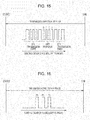
- Fig. 16 illustrates an example of the upper limit current value request pulse which is sent from the MHL transmitting unit 108 to the MHL receiving unit 204.
- the upper limit current value request pulse has a form simplified from the upper limit current value request pulse illustrated in Fig. 14 .
- a long pulse thereof is configured to have Pa, Pb, and Pc which are continued at an equal interval.
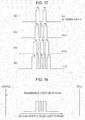
- Figs. 17(a) to (d) illustrate an example of the response pulse which is sent to the MHL transmitting unit 108 from the MHL receiving unit 204.
- the response pulse has a form simplified from the response pulse illustrated in Fig. 15 .
- the response pulse contains information representing a type of upper limit current value.
- the response pulses in Figs. 17 (a) to (d) are examples of a case in which the types of upper limit current value on the MHL receiving unit 204 side are limited to four types of 0 A, 0.5 A, 0.9 A, and 1.5 A.
- the response pulse is configured to have long pulses Pa and Pb before and after zero to three short pulses Pc so as to interpose the short pulses therebetween.
- the MHL receiving unit 204 determines the first long pulse Pa as a start (STX) of the transmission and the last and next long pulse Pb as an end (ETX) of the transmission, and can find out the upper limit current value by counting the number of the short pulses Pc between the long pulses.
- Figs. 17(a), (b), (c), and (d) illustrate response pulses showing that the upper limit current values are 0 A, 0.5 A, 0.9 A, and 1.5 A, respectively.
- Fig. 18 illustrates an example of the response pulse which is sent to the MHL transmitting unit 108 in a case where the upper limit current value on the MHL receiving unit 204 side is 0.5 A.
- the upper limit current value request pulse as the inquiry signal is sent to the MHL receiving unit (MHL sink) 204 of the television 200 from the MHL transmitting unit (MHL source) 108 of the mobile phone 100.
- the response pulse as the response signal returns to the MHL transmitting unit 108 from the MHL receiving unit 204.
- a configuration is considered, in which the inquiry signal is sent to the MHL transmitting unit (MHL source) 108 of the mobile phone 100 from the MHL receiving unit (MHL sink) 204 of the television 200 and, with respect to this, the response signal returns to the MHL receiving unit 204 from the MHL transmitting unit 108.
- a battery power-level request pulse as the inquiry signal is sent to the MHL transmitting unit (MHL source) 108 of the mobile phone 100 from the MHL receiving unit (MHL sink) 204 of the television 200.
- MHL transmitting unit MHL source
- MHL receiving unit MHL sink
- a 4-bit command in the battery power-level request pulse means a battery power-level request. For example, replacement with "1010" is performed.
- the MHL transmitting unit 108 uses the response pulse as illustrated in Fig. 15 described above as the battery power level and respond to the MHL receiving unit 204.
- the 4-bit response indicates that, for example, a tens place of the battery power level (%) is designated. For example, in a case where the battery power level is 80%, the 4-bit response is "1000(8)". In a case where the battery power level is 100%, the 4-bit response is "1010(10)".
- the control unit 201 On the MHL receiving unit (MHL sink) 204 side, that is, the television 200, which receives the response pulse of the battery power level, the control unit 201 generates OSD display data based on the battery power-level information and performs display of the battery power level of the mobile phone 100 on a predetermined portion, for example, on a corner of a screen, of the display panel 209. In this way, a user who views the television 200 can easily know the battery power level and thus, charging progress of the mobile phone 100. Then, the transmission of the battery power-level request pulse from the television 200 to the mobile phone 100 may be automatically performed periodically, or may be performed in response to a user's intentional operation.
- MHL sink MHL sink
- MHL transmitting unit MHL source
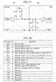
- the state in Fig. 19 becomes a state in which S3 is closed, S4 is opened, and at this time, a voltage between CBUS-GND becomes low.
- R3 (1 k ⁇ ) is switched to R4 (100 k ⁇ ) when S3 is opened and S4 is closed as illustrated in Fig. 20 . Therefore, the voltage between CBUS-GND is increased to be high.
- the source determines that a response pulse is issued from the sink.
- the sink performs transmission to the source by switching the switch opening/closing states; when the voltage is high, the transmission is performed as in Fig. 20 and, when the voltage is low, the transmission is performed as in Fig. 19 .
- the inquiry signal an example of the upper limit current value request pulse and the battery power-level request pulse is shown.
- another inquiry signal it is possible to consider another inquiry signal to the same.
- the 4-bit command in the upper limit current value request pulse in Fig. 14 described above is converted into a value which means the request.
- Fig. 22 illustrates an example of a correlation between the value of the 4-bit command and the meaning thereof.
- “1001” means the upper limit current value request and "1010” means the battery power-level request, as described above. Then, it is shown that "1011” to “1111” are reserved and are not used currently.
- the request pulse is sent through the CBUS and the response pulse in response to that is received through the CBUS.
- the response pulse may not return through the CBUS, necessarily.
- the request pulse is sent to the MHL receiving unit (MHL sink) 204 from the MHL transmitting unit (MHL source) 108, it is considered that the MHL receiving unit (MHL sink) 204 returns the response pulse corresponding to the request pulse through the VBUS which is the power supply line.
- the MHL source device corresponds to the mobile phone 100 and the MHL sink device corresponds to the television 200.
- the MHL source device corresponds to the mobile phone 100 and the MHL sink device corresponds to the television 200.
- a combination of the MHL source device and the MHL sink device is not limited thereto.
- the present technology can achieve the following configuration.
Landscapes
- Engineering & Computer Science (AREA)
- Multimedia (AREA)
- Signal Processing (AREA)
- General Engineering & Computer Science (AREA)
- Software Systems (AREA)
- Computer Networks & Wireless Communication (AREA)
- Telephone Function (AREA)
- Charge And Discharge Circuits For Batteries Or The Like (AREA)
- Two-Way Televisions, Distribution Of Moving Picture Or The Like (AREA)
Applications Claiming Priority (2)
| Application Number | Priority Date | Filing Date | Title |
|---|---|---|---|
| JP2012229143 | 2012-10-16 | ||
| PCT/JP2013/077885 WO2014061624A1 (ja) | 2012-10-16 | 2013-10-15 | 電子機器、電子機器の充電制御方法、電子機器のバッテリ残量表示方法、ソース機器およびシンク機器 |
Publications (3)
| Publication Number | Publication Date |
|---|---|
| EP2911405A1 true EP2911405A1 (de) | 2015-08-26 |
| EP2911405A4 EP2911405A4 (de) | 2016-04-13 |
| EP2911405B1 EP2911405B1 (de) | 2019-12-04 |
Family
ID=50488187
Family Applications (1)
| Application Number | Title | Priority Date | Filing Date |
|---|---|---|---|
| EP13847566.0A Active EP2911405B1 (de) | 2012-10-16 | 2013-10-15 | Elektronische vorrichtung, ladungssteuerungsverfahren für die elektronische vorrichtung, verfahren zur anzeige der verbleibenden batterieladung der elektronischen vorrichtung, quellvorrichtung und senkenvorrichtung |
Country Status (5)
| Country | Link |
|---|---|
| US (1) | US10231017B2 (de) |
| EP (1) | EP2911405B1 (de) |
| JP (1) | JP6237637B2 (de) |
| CN (1) | CN104756508B (de) |
| WO (1) | WO2014061624A1 (de) |
Families Citing this family (5)
| Publication number | Priority date | Publication date | Assignee | Title |
|---|---|---|---|---|
| US20150334333A1 (en) * | 2013-07-30 | 2015-11-19 | Kabushiki Kaisha Toshiba | Electronic device and method for controlling the same |
| TWI630481B (zh) * | 2014-04-04 | 2018-07-21 | 美商萊迪思半導體公司 | 檢測連接至一裝置之多媒體鏈接之方向 |
| CN112118479A (zh) * | 2015-02-02 | 2020-12-22 | 麦克赛尔株式会社 | 广播接收装置和内容输出方法 |
| KR102349363B1 (ko) * | 2015-08-24 | 2022-01-11 | 삼성전자주식회사 | 영상처리시스템, 영상표시장치, 전자장치, 절전형 인터페이스장치 및 영상표시장치의 구동방법 |
| ES2693419B2 (es) | 2017-06-08 | 2019-10-15 | Ruiz Del Arbol Jose Ramon Vazquez | Pavimento de hormigón armado de espesor reducido |
Family Cites Families (17)
| Publication number | Priority date | Publication date | Assignee | Title |
|---|---|---|---|---|
| TW479393B (en) * | 2000-09-27 | 2002-03-11 | Acer Peripherals Inc | Automatic USB charging apparatus and its operating method |
| CN101909190B (zh) * | 2005-09-30 | 2012-09-26 | 松下电器产业株式会社 | 无线传送系统 |
| JP5292776B2 (ja) | 2007-07-19 | 2013-09-18 | ソニー株式会社 | 送信装置、送信装置の電源切換方法、受信装置および受信装置の電源供給方法 |
| JP5636421B2 (ja) * | 2009-04-17 | 2014-12-03 | エスティー‐エリクソン グレノーブル エスエーエスSt−Ericsson Grenoble Sas | Hdmiシステムにおける拡張給電 |
| US8830073B2 (en) * | 2009-12-01 | 2014-09-09 | Apple Inc. | Power converter with reduced power consumption when toggling between sleep and normal modes during device charging |
| US8069356B2 (en) | 2010-01-06 | 2011-11-29 | Apple Inc. | Accessory power management |
| JP2011229110A (ja) * | 2010-03-31 | 2011-11-10 | Toshiba Corp | 電子機器及び電力制御方法 |
| JP5671838B2 (ja) * | 2010-05-21 | 2015-02-18 | ソニー株式会社 | データ送信装置、データ受信装置、データ送信方法およびデータ受信方法 |
| US8396600B2 (en) * | 2010-07-23 | 2013-03-12 | Chevron Phillips Chemical Company Lp | Prediction and control solution for polymerization reactor operation |
| KR20120014801A (ko) * | 2010-08-10 | 2012-02-20 | 삼성전자주식회사 | 컴퓨터 시스템 및 그 제어방법 |
| JP5514364B2 (ja) * | 2010-08-27 | 2014-06-04 | 株式会社日立製作所 | 記憶制御装置及び記憶制御装置の動作モード制御方法 |
| KR101717505B1 (ko) * | 2010-12-02 | 2017-03-17 | 삼성전자주식회사 | 외부 기기 충전 방법 및 이를 이용하는 디스플레이 장치 |
| US9015509B2 (en) | 2011-02-07 | 2015-04-21 | Silicon Image, Inc. | Mechanism for low power standby mode control circuit |
| JP5673172B2 (ja) * | 2011-02-09 | 2015-02-18 | ソニー株式会社 | 電子機器、電子機器における立体画像情報送信方法、および電子機器における立体画像情報受信方法 |
| KR101566174B1 (ko) * | 2011-03-02 | 2015-11-05 | 삼성전자 주식회사 | 영상처리장치 및 그 제어방법 |
| JP2012109990A (ja) * | 2011-12-20 | 2012-06-07 | Toshiba Corp | 電源供給回路 |
| US9269305B2 (en) * | 2012-09-11 | 2016-02-23 | Apple Inc. | Reduced backlight turn on time |
-
2013
- 2013-10-15 JP JP2014542128A patent/JP6237637B2/ja not_active Expired - Fee Related
- 2013-10-15 EP EP13847566.0A patent/EP2911405B1/de active Active
- 2013-10-15 CN CN201380052654.2A patent/CN104756508B/zh not_active Expired - Fee Related
- 2013-10-15 WO PCT/JP2013/077885 patent/WO2014061624A1/ja not_active Ceased
- 2013-10-15 US US14/433,105 patent/US10231017B2/en active Active
Also Published As
| Publication number | Publication date |
|---|---|
| WO2014061624A1 (ja) | 2014-04-24 |
| US10231017B2 (en) | 2019-03-12 |
| EP2911405A4 (de) | 2016-04-13 |
| US20150249862A1 (en) | 2015-09-03 |
| JPWO2014061624A1 (ja) | 2016-09-05 |
| EP2911405B1 (de) | 2019-12-04 |
| CN104756508B (zh) | 2018-09-21 |
| CN104756508A (zh) | 2015-07-01 |
| JP6237637B2 (ja) | 2017-11-29 |
Similar Documents
| Publication | Publication Date | Title |
|---|---|---|
| US20250021404A1 (en) | Multi-interface streaming media system | |
| JP5515919B2 (ja) | 電子機器および接続外部機器のデジタルインタフェース判別方法 | |
| KR101574047B1 (ko) | 타겟 디바이스로 명령을 전송하기 위한 기술 | |
| EP2238530B1 (de) | Entdeckung elektronischer geräte anhand eines steuerbusses | |
| US10038871B2 (en) | Method and device for transmitting and receiving power using HDMI | |
| EP2911405B1 (de) | Elektronische vorrichtung, ladungssteuerungsverfahren für die elektronische vorrichtung, verfahren zur anzeige der verbleibenden batterieladung der elektronischen vorrichtung, quellvorrichtung und senkenvorrichtung | |
| US20090307734A1 (en) | Communication device for providing communication between electronic apparatuses | |
| US10176140B2 (en) | HDMI apparatus of high-definition TV has switching circuit that outputs low-level/ground potential to second pin of HDMI connector if a first signal is not outputted | |
| US9760156B2 (en) | Display apparatus, display system having plural display apparatuses, and method for controlling the display system | |
| JP5943439B2 (ja) | 電子機器、通信システムおよびホットプラグ制御方法 | |
| EP2166530A2 (de) | Flüssigkristallanzeige und Anzeigesystem damit | |
| EP2549360A1 (de) | Anzeigevorrichtung, Host-Vorrichtung, Anzeigesystem, Verfahren zur Steuerung der Anzeigevorrichtung, und das Anzeigesystem | |
| US20180054589A1 (en) | Method for transmitting and receiving power using hdmi and apparatus therefor | |
| CN111031371B (zh) | 单线投屏系统及方法 | |
| US20120005381A1 (en) | Universal serial bus (usb) interface device having functions of high definition conversion and audio supporting | |
| CN102880273A (zh) | 显示设备及其向外接设备供电的方法 | |
| CN100435574C (zh) | Tv中转换高分辨率多媒体接口输入的方法 | |
| CN102510112B (zh) | 对可携式电子装置充电的系统与显示装置 | |
| CN224036061U (zh) | 双屏控制电路 | |
| KR100608047B1 (ko) | Pc와의 인터페이스가 가능한 부가 기능 처리 장치 | |
| CN108920115A (zh) | 一种智能切换pc模式和显示器模式的方法 | |
| JP2013243762A (ja) | 通信装置及び制御方法 | |
| CN101686342A (zh) | 一种具备读卡功能的电视机 | |
| CN102572353A (zh) | 电子装置、控制电子装置的方法、发送装置和接收装置 |
Legal Events
| Date | Code | Title | Description |
|---|---|---|---|
| PUAI | Public reference made under article 153(3) epc to a published international application that has entered the european phase |
Free format text: ORIGINAL CODE: 0009012 |
|
| 17P | Request for examination filed |
Effective date: 20150408 |
|
| AK | Designated contracting states |
Kind code of ref document: A1 Designated state(s): AL AT BE BG CH CY CZ DE DK EE ES FI FR GB GR HR HU IE IS IT LI LT LU LV MC MK MT NL NO PL PT RO RS SE SI SK SM TR |
|
| AX | Request for extension of the european patent |
Extension state: BA ME |
|
| DAX | Request for extension of the european patent (deleted) | ||
| RA4 | Supplementary search report drawn up and despatched (corrected) |
Effective date: 20160315 |
|
| RIC1 | Information provided on ipc code assigned before grant |
Ipc: H04N 21/414 20110101ALI20160309BHEP Ipc: H04N 21/41 20110101AFI20160309BHEP Ipc: H04N 21/443 20110101ALI20160309BHEP |
|
| STAA | Information on the status of an ep patent application or granted ep patent |
Free format text: STATUS: EXAMINATION IS IN PROGRESS |
|
| 17Q | First examination report despatched |
Effective date: 20170821 |
|
| REG | Reference to a national code |
Ref country code: DE Ref legal event code: R079 Ref document number: 602013063718 Country of ref document: DE Free format text: PREVIOUS MAIN CLASS: H04N0021426000 Ipc: H04N0021410000 |
|
| GRAP | Despatch of communication of intention to grant a patent |
Free format text: ORIGINAL CODE: EPIDOSNIGR1 |
|
| STAA | Information on the status of an ep patent application or granted ep patent |
Free format text: STATUS: GRANT OF PATENT IS INTENDED |
|
| RIC1 | Information provided on ipc code assigned before grant |
Ipc: H04N 21/443 20110101ALI20190508BHEP Ipc: H04N 21/414 20110101ALI20190508BHEP Ipc: H04N 21/41 20110101AFI20190508BHEP Ipc: G06F 1/26 20060101ALN20190508BHEP |
|
| INTG | Intention to grant announced |
Effective date: 20190529 |
|
| GRAS | Grant fee paid |
Free format text: ORIGINAL CODE: EPIDOSNIGR3 |
|
| GRAA | (expected) grant |
Free format text: ORIGINAL CODE: 0009210 |
|
| STAA | Information on the status of an ep patent application or granted ep patent |
Free format text: STATUS: THE PATENT HAS BEEN GRANTED |
|
| AK | Designated contracting states |
Kind code of ref document: B1 Designated state(s): AL AT BE BG CH CY CZ DE DK EE ES FI FR GB GR HR HU IE IS IT LI LT LU LV MC MK MT NL NO PL PT RO RS SE SI SK SM TR |
|
| REG | Reference to a national code |
Ref country code: GB Ref legal event code: FG4D |
|
| REG | Reference to a national code |
Ref country code: CH Ref legal event code: EP |
|
| REG | Reference to a national code |
Ref country code: AT Ref legal event code: REF Ref document number: 1211003 Country of ref document: AT Kind code of ref document: T Effective date: 20191215 |
|
| REG | Reference to a national code |
Ref country code: DE Ref legal event code: R096 Ref document number: 602013063718 Country of ref document: DE |
|
| REG | Reference to a national code |
Ref country code: IE Ref legal event code: FG4D |
|
| REG | Reference to a national code |
Ref country code: NL Ref legal event code: MP Effective date: 20191204 |
|
| REG | Reference to a national code |
Ref country code: LT Ref legal event code: MG4D |
|
| PG25 | Lapsed in a contracting state [announced via postgrant information from national office to epo] |
Ref country code: LT Free format text: LAPSE BECAUSE OF FAILURE TO SUBMIT A TRANSLATION OF THE DESCRIPTION OR TO PAY THE FEE WITHIN THE PRESCRIBED TIME-LIMIT Effective date: 20191204 Ref country code: GR Free format text: LAPSE BECAUSE OF FAILURE TO SUBMIT A TRANSLATION OF THE DESCRIPTION OR TO PAY THE FEE WITHIN THE PRESCRIBED TIME-LIMIT Effective date: 20200305 Ref country code: NO Free format text: LAPSE BECAUSE OF FAILURE TO SUBMIT A TRANSLATION OF THE DESCRIPTION OR TO PAY THE FEE WITHIN THE PRESCRIBED TIME-LIMIT Effective date: 20200304 Ref country code: LV Free format text: LAPSE BECAUSE OF FAILURE TO SUBMIT A TRANSLATION OF THE DESCRIPTION OR TO PAY THE FEE WITHIN THE PRESCRIBED TIME-LIMIT Effective date: 20191204 Ref country code: SE Free format text: LAPSE BECAUSE OF FAILURE TO SUBMIT A TRANSLATION OF THE DESCRIPTION OR TO PAY THE FEE WITHIN THE PRESCRIBED TIME-LIMIT Effective date: 20191204 Ref country code: FI Free format text: LAPSE BECAUSE OF FAILURE TO SUBMIT A TRANSLATION OF THE DESCRIPTION OR TO PAY THE FEE WITHIN THE PRESCRIBED TIME-LIMIT Effective date: 20191204 Ref country code: BG Free format text: LAPSE BECAUSE OF FAILURE TO SUBMIT A TRANSLATION OF THE DESCRIPTION OR TO PAY THE FEE WITHIN THE PRESCRIBED TIME-LIMIT Effective date: 20200304 |
|
| PG25 | Lapsed in a contracting state [announced via postgrant information from national office to epo] |
Ref country code: RS Free format text: LAPSE BECAUSE OF FAILURE TO SUBMIT A TRANSLATION OF THE DESCRIPTION OR TO PAY THE FEE WITHIN THE PRESCRIBED TIME-LIMIT Effective date: 20191204 Ref country code: HR Free format text: LAPSE BECAUSE OF FAILURE TO SUBMIT A TRANSLATION OF THE DESCRIPTION OR TO PAY THE FEE WITHIN THE PRESCRIBED TIME-LIMIT Effective date: 20191204 |
|
| PG25 | Lapsed in a contracting state [announced via postgrant information from national office to epo] |
Ref country code: AL Free format text: LAPSE BECAUSE OF FAILURE TO SUBMIT A TRANSLATION OF THE DESCRIPTION OR TO PAY THE FEE WITHIN THE PRESCRIBED TIME-LIMIT Effective date: 20191204 |
|
| PG25 | Lapsed in a contracting state [announced via postgrant information from national office to epo] |
Ref country code: EE Free format text: LAPSE BECAUSE OF FAILURE TO SUBMIT A TRANSLATION OF THE DESCRIPTION OR TO PAY THE FEE WITHIN THE PRESCRIBED TIME-LIMIT Effective date: 20191204 Ref country code: ES Free format text: LAPSE BECAUSE OF FAILURE TO SUBMIT A TRANSLATION OF THE DESCRIPTION OR TO PAY THE FEE WITHIN THE PRESCRIBED TIME-LIMIT Effective date: 20191204 Ref country code: PT Free format text: LAPSE BECAUSE OF FAILURE TO SUBMIT A TRANSLATION OF THE DESCRIPTION OR TO PAY THE FEE WITHIN THE PRESCRIBED TIME-LIMIT Effective date: 20200429 Ref country code: NL Free format text: LAPSE BECAUSE OF FAILURE TO SUBMIT A TRANSLATION OF THE DESCRIPTION OR TO PAY THE FEE WITHIN THE PRESCRIBED TIME-LIMIT Effective date: 20191204 Ref country code: CZ Free format text: LAPSE BECAUSE OF FAILURE TO SUBMIT A TRANSLATION OF THE DESCRIPTION OR TO PAY THE FEE WITHIN THE PRESCRIBED TIME-LIMIT Effective date: 20191204 Ref country code: RO Free format text: LAPSE BECAUSE OF FAILURE TO SUBMIT A TRANSLATION OF THE DESCRIPTION OR TO PAY THE FEE WITHIN THE PRESCRIBED TIME-LIMIT Effective date: 20191204 |
|
| PG25 | Lapsed in a contracting state [announced via postgrant information from national office to epo] |
Ref country code: SM Free format text: LAPSE BECAUSE OF FAILURE TO SUBMIT A TRANSLATION OF THE DESCRIPTION OR TO PAY THE FEE WITHIN THE PRESCRIBED TIME-LIMIT Effective date: 20191204 Ref country code: SK Free format text: LAPSE BECAUSE OF FAILURE TO SUBMIT A TRANSLATION OF THE DESCRIPTION OR TO PAY THE FEE WITHIN THE PRESCRIBED TIME-LIMIT Effective date: 20191204 Ref country code: IS Free format text: LAPSE BECAUSE OF FAILURE TO SUBMIT A TRANSLATION OF THE DESCRIPTION OR TO PAY THE FEE WITHIN THE PRESCRIBED TIME-LIMIT Effective date: 20200404 |
|
| REG | Reference to a national code |
Ref country code: DE Ref legal event code: R097 Ref document number: 602013063718 Country of ref document: DE |
|
| REG | Reference to a national code |
Ref country code: AT Ref legal event code: MK05 Ref document number: 1211003 Country of ref document: AT Kind code of ref document: T Effective date: 20191204 |
|
| PLBE | No opposition filed within time limit |
Free format text: ORIGINAL CODE: 0009261 |
|
| STAA | Information on the status of an ep patent application or granted ep patent |
Free format text: STATUS: NO OPPOSITION FILED WITHIN TIME LIMIT |
|
| PG25 | Lapsed in a contracting state [announced via postgrant information from national office to epo] |
Ref country code: DK Free format text: LAPSE BECAUSE OF FAILURE TO SUBMIT A TRANSLATION OF THE DESCRIPTION OR TO PAY THE FEE WITHIN THE PRESCRIBED TIME-LIMIT Effective date: 20191204 |
|
| 26N | No opposition filed |
Effective date: 20200907 |
|
| PG25 | Lapsed in a contracting state [announced via postgrant information from national office to epo] |
Ref country code: SI Free format text: LAPSE BECAUSE OF FAILURE TO SUBMIT A TRANSLATION OF THE DESCRIPTION OR TO PAY THE FEE WITHIN THE PRESCRIBED TIME-LIMIT Effective date: 20191204 Ref country code: PL Free format text: LAPSE BECAUSE OF FAILURE TO SUBMIT A TRANSLATION OF THE DESCRIPTION OR TO PAY THE FEE WITHIN THE PRESCRIBED TIME-LIMIT Effective date: 20191204 Ref country code: AT Free format text: LAPSE BECAUSE OF FAILURE TO SUBMIT A TRANSLATION OF THE DESCRIPTION OR TO PAY THE FEE WITHIN THE PRESCRIBED TIME-LIMIT Effective date: 20191204 |
|
| PG25 | Lapsed in a contracting state [announced via postgrant information from national office to epo] |
Ref country code: IT Free format text: LAPSE BECAUSE OF FAILURE TO SUBMIT A TRANSLATION OF THE DESCRIPTION OR TO PAY THE FEE WITHIN THE PRESCRIBED TIME-LIMIT Effective date: 20191204 |
|
| REG | Reference to a national code |
Ref country code: CH Ref legal event code: PL |
|
| PG25 | Lapsed in a contracting state [announced via postgrant information from national office to epo] |
Ref country code: LU Free format text: LAPSE BECAUSE OF NON-PAYMENT OF DUE FEES Effective date: 20201015 Ref country code: MC Free format text: LAPSE BECAUSE OF FAILURE TO SUBMIT A TRANSLATION OF THE DESCRIPTION OR TO PAY THE FEE WITHIN THE PRESCRIBED TIME-LIMIT Effective date: 20191204 |
|
| REG | Reference to a national code |
Ref country code: BE Ref legal event code: MM Effective date: 20201031 |
|
| PG25 | Lapsed in a contracting state [announced via postgrant information from national office to epo] |
Ref country code: BE Free format text: LAPSE BECAUSE OF NON-PAYMENT OF DUE FEES Effective date: 20201031 Ref country code: CH Free format text: LAPSE BECAUSE OF NON-PAYMENT OF DUE FEES Effective date: 20201031 Ref country code: LI Free format text: LAPSE BECAUSE OF NON-PAYMENT OF DUE FEES Effective date: 20201031 |
|
| PG25 | Lapsed in a contracting state [announced via postgrant information from national office to epo] |
Ref country code: IE Free format text: LAPSE BECAUSE OF NON-PAYMENT OF DUE FEES Effective date: 20201015 |
|
| PG25 | Lapsed in a contracting state [announced via postgrant information from national office to epo] |
Ref country code: TR Free format text: LAPSE BECAUSE OF FAILURE TO SUBMIT A TRANSLATION OF THE DESCRIPTION OR TO PAY THE FEE WITHIN THE PRESCRIBED TIME-LIMIT Effective date: 20191204 Ref country code: MT Free format text: LAPSE BECAUSE OF FAILURE TO SUBMIT A TRANSLATION OF THE DESCRIPTION OR TO PAY THE FEE WITHIN THE PRESCRIBED TIME-LIMIT Effective date: 20191204 Ref country code: CY Free format text: LAPSE BECAUSE OF FAILURE TO SUBMIT A TRANSLATION OF THE DESCRIPTION OR TO PAY THE FEE WITHIN THE PRESCRIBED TIME-LIMIT Effective date: 20191204 |
|
| PG25 | Lapsed in a contracting state [announced via postgrant information from national office to epo] |
Ref country code: MK Free format text: LAPSE BECAUSE OF FAILURE TO SUBMIT A TRANSLATION OF THE DESCRIPTION OR TO PAY THE FEE WITHIN THE PRESCRIBED TIME-LIMIT Effective date: 20191204 |
|
| P01 | Opt-out of the competence of the unified patent court (upc) registered |
Effective date: 20230527 |
|
| PGFP | Annual fee paid to national office [announced via postgrant information from national office to epo] |
Ref country code: GB Payment date: 20230920 Year of fee payment: 11 |
|
| PGFP | Annual fee paid to national office [announced via postgrant information from national office to epo] |
Ref country code: FR Payment date: 20230920 Year of fee payment: 11 |
|
| PGFP | Annual fee paid to national office [announced via postgrant information from national office to epo] |
Ref country code: DE Payment date: 20230920 Year of fee payment: 11 |
|
| REG | Reference to a national code |
Ref country code: DE Ref legal event code: R119 Ref document number: 602013063718 Country of ref document: DE |
|
| GBPC | Gb: european patent ceased through non-payment of renewal fee |
Effective date: 20241015 |
|
| PG25 | Lapsed in a contracting state [announced via postgrant information from national office to epo] |
Ref country code: DE Free format text: LAPSE BECAUSE OF NON-PAYMENT OF DUE FEES Effective date: 20250501 |
|
| PG25 | Lapsed in a contracting state [announced via postgrant information from national office to epo] |
Ref country code: GB Free format text: LAPSE BECAUSE OF NON-PAYMENT OF DUE FEES Effective date: 20241015 |
|
| PG25 | Lapsed in a contracting state [announced via postgrant information from national office to epo] |
Ref country code: FR Free format text: LAPSE BECAUSE OF NON-PAYMENT OF DUE FEES Effective date: 20241031 |