EP2913378A1 - Target für ultraviolettlichterzeugung, durch einen elektronenstrahl erregte ultraviolettlichtquelle und herstellungsverfahren für das target für ultraviolettlichterzeugung - Google Patents
Target für ultraviolettlichterzeugung, durch einen elektronenstrahl erregte ultraviolettlichtquelle und herstellungsverfahren für das target für ultraviolettlichterzeugung Download PDFInfo
- Publication number
- EP2913378A1 EP2913378A1 EP13849168.3A EP13849168A EP2913378A1 EP 2913378 A1 EP2913378 A1 EP 2913378A1 EP 13849168 A EP13849168 A EP 13849168A EP 2913378 A1 EP2913378 A1 EP 2913378A1
- Authority
- EP
- European Patent Office
- Prior art keywords
- ultraviolet light
- target
- film
- heat treatment
- light generation
- Prior art date
- Legal status (The legal status is an assumption and is not a legal conclusion. Google has not performed a legal analysis and makes no representation as to the accuracy of the status listed.)
- Granted
Links
Images










Classifications
-
- H—ELECTRICITY
- H01—ELECTRIC ELEMENTS
- H01J—ELECTRIC DISCHARGE TUBES OR DISCHARGE LAMPS
- H01J63/00—Cathode-ray or electron-stream lamps
- H01J63/06—Lamps with luminescent screen excited by the ray or stream
-
- C—CHEMISTRY; METALLURGY
- C09—DYES; PAINTS; POLISHES; NATURAL RESINS; ADHESIVES; COMPOSITIONS NOT OTHERWISE PROVIDED FOR; APPLICATIONS OF MATERIALS NOT OTHERWISE PROVIDED FOR
- C09K—MATERIALS FOR MISCELLANEOUS APPLICATIONS, NOT PROVIDED FOR ELSEWHERE
- C09K11/00—Luminescent materials, e.g. electroluminescent or chemiluminescent
- C09K11/08—Luminescent materials, e.g. electroluminescent or chemiluminescent containing inorganic luminescent materials
- C09K11/77—Luminescent materials, e.g. electroluminescent or chemiluminescent containing inorganic luminescent materials containing rare earth metals
- C09K11/7766—Luminescent materials, e.g. electroluminescent or chemiluminescent containing inorganic luminescent materials containing rare earth metals containing two or more rare earth metals
- C09K11/7774—Aluminates
-
- C—CHEMISTRY; METALLURGY
- C09—DYES; PAINTS; POLISHES; NATURAL RESINS; ADHESIVES; COMPOSITIONS NOT OTHERWISE PROVIDED FOR; APPLICATIONS OF MATERIALS NOT OTHERWISE PROVIDED FOR
- C09K—MATERIALS FOR MISCELLANEOUS APPLICATIONS, NOT PROVIDED FOR ELSEWHERE
- C09K11/00—Luminescent materials, e.g. electroluminescent or chemiluminescent
- C09K11/08—Luminescent materials, e.g. electroluminescent or chemiluminescent containing inorganic luminescent materials
- C09K11/77—Luminescent materials, e.g. electroluminescent or chemiluminescent containing inorganic luminescent materials containing rare earth metals
- C09K11/7766—Luminescent materials, e.g. electroluminescent or chemiluminescent containing inorganic luminescent materials containing rare earth metals containing two or more rare earth metals
- C09K11/77742—Silicates
-
- C—CHEMISTRY; METALLURGY
- C23—COATING METALLIC MATERIAL; COATING MATERIAL WITH METALLIC MATERIAL; CHEMICAL SURFACE TREATMENT; DIFFUSION TREATMENT OF METALLIC MATERIAL; COATING BY VACUUM EVAPORATION, BY SPUTTERING, BY ION IMPLANTATION OR BY CHEMICAL VAPOUR DEPOSITION, IN GENERAL; INHIBITING CORROSION OF METALLIC MATERIAL OR INCRUSTATION IN GENERAL
- C23C—COATING METALLIC MATERIAL; COATING MATERIAL WITH METALLIC MATERIAL; SURFACE TREATMENT OF METALLIC MATERIAL BY DIFFUSION INTO THE SURFACE, BY CHEMICAL CONVERSION OR SUBSTITUTION; COATING BY VACUUM EVAPORATION, BY SPUTTERING, BY ION IMPLANTATION OR BY CHEMICAL VAPOUR DEPOSITION, IN GENERAL
- C23C16/00—Chemical coating by decomposition of gaseous compounds, without leaving reaction products of surface material in the coating, i.e. chemical vapour deposition [CVD] processes
- C23C16/22—Chemical coating by decomposition of gaseous compounds, without leaving reaction products of surface material in the coating, i.e. chemical vapour deposition [CVD] processes characterised by the deposition of inorganic material, other than metallic material
- C23C16/30—Deposition of compounds, mixtures or solid solutions, e.g. borides, carbides, nitrides
- C23C16/40—Oxides
-
- H—ELECTRICITY
- H01—ELECTRIC ELEMENTS
- H01J—ELECTRIC DISCHARGE TUBES OR DISCHARGE LAMPS
- H01J63/00—Cathode-ray or electron-stream lamps
- H01J63/02—Details, e.g. electrode, gas filling, shape of vessel
- H01J63/04—Vessels provided with luminescent coatings; Selection of materials for the coatings
Definitions
- One aspect of the present invention relates to a target for ultraviolet light generation, an electron-beam-excited ultraviolet light source, and a method for manufacturing a target for ultraviolet light generation.
- Patent Literature 1 describes the use of a single crystal containing praseodymium (Pr) as a material for a scintillator employed in PET devices.
- Patent Literature 2 discloses a technique concerning an illumination system in which a wavelength of light emitted from a light-emitting diode is converted by a phosphor so as to attain white light.
- Electron tubes such as mercury-xenon lamps and deuterium lamps have conventionally been used as ultraviolet light sources.
- these ultraviolet light sources are low in light emission efficiency and large in size and have problems in terms of stability and life.
- electron-beam-excited ultraviolet light sources equipped with a structure for exciting ultraviolet light by irradiating a target with an electron beam have been known as another type of ultraviolet light sources.
- the electron-beam-excited ultraviolet light sources are expected to become light sources in the field of optical measurement taking advantage of their high stability, for sterilization and disinfection making use of their low power consumption, or for medical care and biochemistry utilizing their high wavelength selectivity.
- the electron-beam-excited ultraviolet light sources also have a merit that their power consumption is lower than that of mercury lamps and the like.
- the electron-beam-excited ultraviolet light sources are also demanded to improve their ultraviolet light generation efficiency further. It is an object of one aspect of the present invention to provide a target for ultraviolet light generation, an electron-beam-excited ultraviolet light source, and a method for manufacturing a target for ultraviolet light generation, which can enhance the ultraviolet light generation efficiency.
- a second target for ultraviolet light generation in accordance with one aspect of the present invention comprises a substrate adapted to transmit ultraviolet light therethrough and a light-emitting layer disposed on the substrate and generating ultraviolet light in response to an electron beam, the light-emitting layer including a polycrystalline film constituted by a rare-earth-containing aluminum garnet polycrystal doped with an activator, the polycrystalline film having an ultraviolet light emission peak wavelength of 300 nm or shorter.
- the inventors thought of using an oxide crystal containing Lu and Si doped with an activator (such as LPS and LSO) or a rare-earth-containing aluminum garnet crystal doped with an activator (such as LuAG and YAG) as a target for ultraviolet light generation.
- an activator such as LPS and LSO
- a rare-earth-containing aluminum garnet crystal doped with an activator such as LuAG and YAG
- single crystals such as those described in the prior art literature is hard to yield sufficient ultraviolet light generation efficiency.
- polycrystals are used in a substrate form as they are, on the other hand, their thickness lowers transmittance for ultraviolet light and increases manufacturing cost.
- the first target for ultraviolet light generation in accordance with one aspect of the present invention can effectively enhance the ultraviolet light emission efficiency as compared with the case of single crystals, since its light-emitting layer contains a polycrystalline film constituted by an oxide polycrystal containing Lu and Si doped with an activator.
- the oxide polycrystal may include at least one of Lu 2 Si 2 O 7 (LPS) and Lu 2 SiO 5 (LSO).
- the activator may be Pr.
- the rare-earth-containing aluminum garnet polycrystal may be Lu 3 Al 5 O 12 (LuAG), the activator being at least one of Sc, La, and Bi.
- the rare-earth-containing aluminum garnet polycrystal may also be Y 3 Al 5 O 12 (YAG), the activator being at least one of Sc and La.
- the polycrystalline film may have a thickness of at least 0.1 ⁇ m but not more than 10 ⁇ m. According to tests and studies conducted by the inventors, the thickness of the polycrystalline film may be at least 0.1 ⁇ m in order for electron beams to contribute to light emission without passing therethrough and may be 10 ⁇ m or less from the viewpoint of productivity. The polycrystalline film having such a thickness can enhance the ultraviolet light emission more effectively.
- the substrate may be constituted by sapphire, silica, or rock crystal. This enables the substrate to transmit ultraviolet light therethrough and endure the temperature of heat treatment of the light-emitting layer.
- the electron-beam-excited ultraviolet light source in accordance with one aspect of the present invention comprises any of the targets for ultraviolet light generation mentioned above and an electron source providing the target with the electron beam.
- This electron-beam-excited ultraviolet light source can enhance the ultraviolet light generation efficiency while suppressing the manufacturing cost by having any of the targets for ultraviolet light generation mentioned above.
- a first method for manufacturing a target for ultraviolet light generation in accordance with one aspect of the present invention comprises a first step of vapor-depositing an activator and an oxide containing Lu and Si on a substrate adapted to transmit ultraviolet light therethrough, so as to form a film, and a second step of turning the film into a polycrystal by heat treatment.
- a second method for manufacturing a target for ultraviolet light generation in accordance with one aspect of the present invention comprises a first step of vapor-depositing an activator having an ultraviolet light emission peak wavelength of 300 nm or shorter and a material for a rare-earth-containing aluminum garnet crystal, so as to form a film, and a second step of turning the film into a polycrystal by heat treatment.
- the first step forms an amorphous film on an ultraviolet-light-transmissive substrate.
- the amorphous film hardly excites ultraviolet light even when irradiated with electron beams.
- Heat-treating (annealing) the amorphous film in the second step as in these manufacturing methods can turn the amorphous film into a polycrystal. That is, the above-mentioned first manufacturing method can favorably manufacture a target for ultraviolet light generation comprising a polycrystalline film constituted by an oxide polycrystal containing Lu and Si doped with an activator.
- the above-mentioned second manufacturing method can also favorably manufacture a target for ultraviolet light generation comprising a polycrystalline film constituted by a rare-earth-containing aluminum garnet crystal doped with an activator.
- the first and second steps may be performed concurrently.
- the film may have a thickness of at least 0.1 ⁇ m but not more than 10 ⁇ m after the heat treatment in the second step. This can more effectively enhance the ultraviolet light emission efficiency.
- the surroundings of the film may be at an atmospheric pressure during the heat treatment in the second step.
- the surroundings of the film may be in a vacuum.
- the target for ultraviolet light generation, electron-beam-excited ultraviolet light source, and method for manufacturing a target for ultraviolet light generation in accordance with one aspect of the present invention can enhance the ultraviolet light generation efficiency.
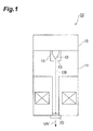
- Fig. 1 is a schematic view illustrating an inner structure of an electron-beam-excited ultraviolet light source 10 in accordance with an embodiment.
- an electron source 12 and an extraction electrode 13 are arranged on the upper end side within a glass envelope (electron tube) 11 evacuated under vacuum.
- an appropriate extraction voltage is applied between the electron source 12 and extraction electrode 13 from a power supply part 16
- an electron beam EB accelerated by a high voltage is emitted from the electron source 12.
- the electron source 12 one emitting an electron beam having a large area (e.g., cold cathodes such as carbon nanotubes or hot cathodes) can be used.
- a target 20 for ultraviolet light generation is arranged on the lower end side within the envelope 11.
- the target 20 is set to the ground potential, for example, while a high negative voltage is applied from the power supply part 16 to the electron source 12.
- the target 20 is irradiated with the electron beam EB emitted from the electron source 12.
- the target 20 is excited in response to the electron beam EB and generates ultraviolet light UV.
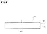
- the light-emitting layer 22 is excited in response to the electron beam EB illustrated in Fig. 1 and generates the ultraviolet light UV.
- the light-emitting layer 22 includes a polycrystalline film formed by turning an oxide containing Lu and Si doped with an activator into a polycrystal.
- Preferred examples of such an oxide polycrystal include Lu 2 Si 2 O 7 (LPS) and Lu 2 SiO 5 (LSO) polycrystals doped with a rare-earth element (Pr in an example) serving as an activator.
- LPS Lu 2 Si 2 O 7
- LSO Lu 2 SiO 5
- Different kinds of the oxide crystal e.g., LPS and LSO
- a preferred thickness of the polycrystalline film is at least 0.1 ⁇ m but not more than 10 ⁇ m.
- a preferred activator content is at least 0.001 atom % but not more than 10 atom %.
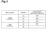
- Fig. 3 is a chart listing specific examples of the rare-earth-containing aluminum garnet crystal doped with an activator which can be used in the light-emitting layer 22 of this embodiment.
- Fig. 3 illustrates ultraviolet light emission peak wavelengths (unit: nm) corresponding to combinations of activators and base materials.
- examples of the rare-earth-containing aluminum garnet crystal doped with an activator include La:LuAG, Sc:LuAG, Bi:LuAG, La:YAG, and Sc:YAG. Their light emission peak wavelengths are not longer than 300 nm and vary depending on the activator content.
- different kinds of rare-earth-containing aluminum garnet crystals e.g., LuAG and YAG
- different kinds of activators e.g., at least two of La, Sc, and Bi
- the laser ablation device 50 further comprises a rotary holder 55, a heater 56 for heating the substrate 21, and a gas inlet 57 for feeding an oxygen gas into the vacuum container 51.
- the rotary holder 55 supports the substrate 21 arranged above the material 53.
- the rotary holder 55 holds the substrate 21 rotatably about an axis connecting the material 53 and substrate 21, while exposing the principal surface 21a of the substrate 21 against the material 53.
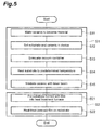
- the substrate 21 is prepared and installed on the rotary holder 55 of the laser ablation device 50, while the material 53 made in the step S11 is mounted on the sample mount 52 (step S12).
- the vacuum container 51 is evacuated (step S 13), and the heater 56 heats the substrate 21 to a predetermined temperature (e.g., 800°C) (step S14).
- the material 53 is irradiated with the laser beam B while feeding the oxygen gas into the vacuum container 51 from the gas inlet 57 (step S15).
- the material 53 evaporates in response to the laser beam B and scatters within the vacuum container 51. A part of the scattered material 53 adheres to the principal surface 21a of the substrate 21, thereby forming an amorphous film.
- the amorphous film formed on the principal surface 21a of the substrate 21 is heat-treated, so as to become a polycrystal (second step S2).
- the substrate 21 having the amorphous film formed thereon is taken out of the laser ablation device 50 and put into a heat treatment furnace (step S21).
- the temperature in the heat treatment furnace is set higher than 1000°C, for example, and this temperature is maintained for a predetermined time, so as to subject the amorphous film on the substrate 21 to heat treatment (annealing) (step S22).
- the heat-treated amorphous film becomes a polycrystal at this time.
- the target 20 in accordance with this embodiment can effectively enhance the ultraviolet light generation efficiency as compared with the case of single crystals. Further, since the above-mentioned polycrystalline film is formed on the ultraviolet-light-transmissive substrate 21, the target in accordance with this embodiment can suppress the manufacturing cost as compared with the case using the polycrystalline substrate and enhance the transmittance for ultraviolet light.
- the substrate 21 is preferably made of sapphire, silica, or rock crystal as in this embodiment. This enables the substrate 21 to transmit ultraviolet light therethrough and the amorphous film to be heat-treated at high temperature in the step S22.
- the polycrystalline film of the light-emitting layer 22 has a thickness of at least 0.1 ⁇ m but not more than 10 ⁇ m as in this embodiment.
- the thickness of the polycrystalline film is preferably at least 0.1 ⁇ m in order for electron beams to contribute to light emission without passing therethrough and preferably 10 ⁇ m or less from the viewpoint of productivity.
- the polycrystalline film having such a thickness can enhance the ultraviolet light emission more effectively.
- the manufacturing method of this embodiment vapor-deposits an amorphous film on the substrate 21 and then heat-treats the amorphous film. While the first step S1 forms an amorphous film on the substrate 21, ultraviolet light hardly occurs even when the amorphous film is irradiated with electron beams. By contrast, heat-treating the amorphous film in the second step can turn the amorphous film into a polycrystalline film, whereby a target for ultraviolet light generation which generates ultraviolet light with a high efficiency can be manufactured.
- the first and second steps S1 and S2 may be performed concurrently.
- the first to sixth examples to be explained in the following are examples concerning the case where the polycrystalline film of the light-emitting layer 22 is constituted by a Pr:LSO polycrystal.
- the facts found out from these examples seem to be the same in oxide polycrystals containing Lu and Si doped with an activator having the same characteristics as those of the Pr:LSO polycrystal, e.g., Pr:LPS polycrystal.
- an LSO-containing ceramic including 0.5 atom % of Pr was made as the material 53. Subsequently, this Pr:LSO-containing ceramic was mounted on the sample mount 52 of the laser ablation device 50, while a sapphire substrate having a diameter of 2 inch was installed on the rotary holder 55. The distance between the Pr:LSO-containing ceramic and sapphire substrate was 150 mm. Thereafter, the vacuum container 51 was evacuated, and the sapphire substrate was heated to 500°C. Then, while feeding the oxygen gas into the vacuum container 51, the material 53 was irradiated with the laser beam B for 120 min, so as to make an amorphous film.
- a KrF excimer laser (150 mJ, 40 Hz) was used as a laser source for the laser beam B. Thereafter, the sapphire substrate was put into a heat treatment furnace, and the sapphire substrate and amorphous film were heated for 2 hr at 1200°C in a vacuum (10 -2 Pa).
- Fig. 6(a) is a graph illustrating results of X-ray diffractometry of the amorphous film before the heat treatment.
- Fig. 6(b) is a graph illustrating results of X-ray diffractometry of the film after the heat treatment.
- these graphs While only diffraction lines deriving from Lu 2 O 3 (indicated by crosses in the graph) and those with large half-widths were observed before the heat treatment, diffraction lines deriving from Pr:LSO crystals (indicated by circles in the graph) were observed after the heat treatment. It is seen from these graphs that the amorphous film has been changed into a Pr:LSO polycrystalline film by the heat treatment.
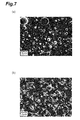
- Figs. 7(a) and 7(b) are SEM photographs concerning the surface of the Pr:LSO film before and after the heat treatment, respectively. Referring to Fig. 7(b) , a region subdivided into sections on the order of several micrometers is observed unlike Fig. 7(a) . It is seen from this fact that the amorphous film has been changed into a Pr:LSO polycrystalline film by the heat treatment.
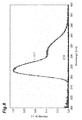
- Fig. 8 is a graph illustrating spectra of ultraviolet light obtained by irradiating the Pr:LSO film with an electron beam.
- graphs G11 and G12 represent light emission spectra of the Pr:LSO film after and before the heat treatment, respectively.
- the film before the heat treatment did not emit light.
- the electron beam had an acceleration voltage of 10 kV, an intensity (amperage) of 100 ⁇ A, and a diameter of 2 mm.
- the amorphous film before the heat treatment hardly generated ultraviolet light even when irradiated with the electron beam.
- the polycrystalline Pr:LSO film after the heat treatment favorably generated ultraviolet light upon irradiation with the electron beam.
- the atmosphere at the time of heat treatment which was a vacuum in the first example, was the air.
- the other steps, conditions, and the like are the same as those of the first example.
- results of X-ray diffractometry of the Pr:LSO film made by this example diffraction lines deriving from Pr:LSO crystals were observed as in Fig. 6(b) .
- Fig. 9 is a graph illustrating spectra of ultraviolet light obtained by irradiating the Pr:LSO film with an electron beam.
- graphs G21 and G22 represent light emission spectra of the Pr:LSO films made by the first example (heat treatment in a vacuum) and the second example (heat treatment in the air), respectively.
- the electron beam had an acceleration voltage of 10 kV, an intensity (amperage) of 100 ⁇ A, and a diameter of 2 mm.
- the peak intensity of ultraviolet light generated by irradiation with the electron beam is much higher (i.e., light emission efficiency is much higher) in the Pr:LSO film heat-treated in the air than in the Pr:LSO film heat-treated in a vacuum.
- Fig. 10 is a graph illustrating a spectrum of ultraviolet light obtained by irradiating a Pr:LSO polycrystal-containing substrate with an electron beam under the same condition as with this example as a comparative example.
- graph G31 represents a light emission spectrum concerning the Pr:LSO polycrystal-containing substrate
- graph G32 is identical to the graph G22 of Fig. 9 .
- the peak intensity of ultraviolet light generated by irradiation with the electron beam is much higher (i.e., light emission efficiency is much higher) in the Pr:LSO polycrystalline film than in the Pr:LSO polycrystal-containing substrate.
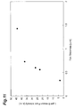
- Fig. 11 is a graph plotting the resulting relationship between the thickness of the Pr:LSO polycrystalline film and the peak intensity of ultraviolet light.
- the thickness of the Pr:LSO polycrystalline film is smaller than a certain value (about 800 nm), the peak intensity of ultraviolet light is higher as the Pr:LSO polycrystalline film is thicker, thereby enhancing the light emission efficiency.
- the thickness of the Pr:LSO polycrystalline film exceeds this value, however, the increase in peak intensity of ultraviolet light is small. It is also seen from this graph that a sufficiently practical ultraviolet light intensity (light emission efficiency) is obtained when the thickness of the Pr:LSO polycrystalline film is 0.1 ⁇ m or greater.
- amorphous films were made by vapor-depositing a material containing Pr:LSO. Two of these amorphous films were heat-treated in a vacuum at temperatures of 1000°C and 1200°C, respectively, so as to make two Pr:LSO polycrystalline films. The remaining one was not heat-treated.
- the other steps, conditions, and the like are the same as those of the first example.
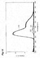
- Each of thus made three Pr:LSO films was irradiated with an electron beam (with an acceleration voltage of 10 kV and an intensity (amperage) of 100 ⁇ A), and the spectrum of generated ultraviolet light was measured.
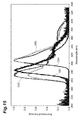
- Fig. 12 is a graph illustrating the measured spectra.
- graphs G40, G41, and G42 represent the respective cases without heat treatment and with heat treatment at temperatures of 1000°C and 1200°C.
- the peak intensity of ultraviolet light increases as the heat treatment temperature of the Pr:LSO film rises, thereby yielding higher light emission efficiency.
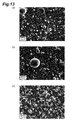
- Fig. 13 is an SEM photograph concerning the surface of the Pr:LSO polycrystalline film after the heat treatment.
- Figs. 13(a), 13(b), and 13(c) illustrate the Pr:LSO film surface in the respective cases without heat treatment and with heat treatment at temperatures of 1000°C and 1200°C. It is seen from Fig. 13 that the crystallization of Pr:LSO advances as the heat treatment temperature is higher.
- amorphous films were made by vapor-depositing a material containing Pr:LSO. Two of these amorphous films were heat-treated in the air at temperatures of 1200°C and 1400°C, respectively, so as to make two Pr:LSO polycrystalline films. The remaining one was not heat-treated.
- the other steps, conditions, and the like are the same as those of the first example.
- Each of thus made three Pr:LSO films was irradiated with an electron beam (with an acceleration voltage of 10 kV and an intensity (amperage) of 100 ⁇ A), and the spectrum of generated ultraviolet light was measured.
- Fig. 14 is a graph illustrating the measured spectra.
- graphs G50, G51, and G52 represent the respective cases without heat treatment and with heat treatment at temperatures of 1000°C and 1200°C.
- substantially the same light emission characteristic was obtained whether the heat treatment temperature of the Pr:LSO film was 1200°C or 1400°C when the heat treatment was performed in the air.
- the light emission peak intensity in the case where the atmosphere at the time of heat treatment was at the atmospheric pressure was about 1.5 times that in the case where the atmosphere at the time of heat treatment was a vacuum. Therefore, the atmosphere at the time of heat treatment is more preferably at the atmospheric pressure.
- the heat treatment temperature is preferably at least 1000°C. It will be more preferred if the heat treatment temperature is 1200°C to 1900°C in particular.
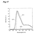
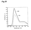
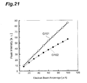
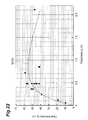
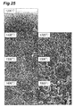
- amorphous films were made by vapor-depositing a material containing Pr:LSO and then heat-treated (for 2 hr) in a heat treatment furnace with a vacuum atmosphere at respective temperatures of 1000°C, 1200°C, 1400°C, and 1500°C, so as to form Pr:LSO polycrystalline films.
- the other steps, conditions, and the like are the same as those of the first example.
- Each of thus made Pr:LSO polycrystalline films was irradiated with an electron beam (with an acceleration voltage of 10 kV and an intensity (amperage) of 100 ⁇ A), and the spectrum of generated ultraviolet light was measured.
Landscapes
- Chemical & Material Sciences (AREA)
- Engineering & Computer Science (AREA)
- Materials Engineering (AREA)
- Organic Chemistry (AREA)
- Inorganic Chemistry (AREA)
- General Chemical & Material Sciences (AREA)
- Chemical Kinetics & Catalysis (AREA)
- Mechanical Engineering (AREA)
- Metallurgy (AREA)
- Luminescent Compositions (AREA)
- Discharge Lamps And Accessories Thereof (AREA)
Applications Claiming Priority (2)
| Application Number | Priority Date | Filing Date | Title |
|---|---|---|---|
| JP2012233973A JP5580865B2 (ja) | 2012-10-23 | 2012-10-23 | 紫外光発生用ターゲット、電子線励起紫外光源、及び紫外光発生用ターゲットの製造方法 |
| PCT/JP2013/074129 WO2014065028A1 (ja) | 2012-10-23 | 2013-09-06 | 紫外光発生用ターゲット、電子線励起紫外光源、及び紫外光発生用ターゲットの製造方法 |
Publications (3)
| Publication Number | Publication Date |
|---|---|
| EP2913378A1 true EP2913378A1 (de) | 2015-09-02 |
| EP2913378A4 EP2913378A4 (de) | 2016-09-14 |
| EP2913378B1 EP2913378B1 (de) | 2017-10-11 |
Family
ID=50544409
Family Applications (1)
| Application Number | Title | Priority Date | Filing Date |
|---|---|---|---|
| EP13849168.3A Not-in-force EP2913378B1 (de) | 2012-10-23 | 2013-09-06 | Target für ultraviolettlichterzeugung, durch einen elektronenstrahl erregte ultraviolettlichtquelle und herstellungsverfahren für das target für ultraviolettlichterzeugung |
Country Status (6)
| Country | Link |
|---|---|
| US (1) | US9240313B2 (de) |
| EP (1) | EP2913378B1 (de) |
| JP (1) | JP5580865B2 (de) |
| KR (1) | KR20150079628A (de) |
| CN (1) | CN104755583B (de) |
| WO (1) | WO2014065028A1 (de) |
Cited By (3)
| Publication number | Priority date | Publication date | Assignee | Title |
|---|---|---|---|---|
| EP3385356A4 (de) * | 2015-11-30 | 2019-05-22 | Dyden Corporation | Ultraviolettlichtemittierender phosphor, lichtemittierendes element und lichtemittierende vorrichtung |
| EP3552225A4 (de) * | 2016-12-08 | 2020-09-09 | LightLab Sweden AB | Eine zur emission von uv-licht angepasste feldemissionslichtquelle |
| US10863752B2 (en) | 2015-10-29 | 2020-12-15 | National Institute of Technology | Plasma sterilization device |
Families Citing this family (7)
| Publication number | Priority date | Publication date | Assignee | Title |
|---|---|---|---|---|
| JP5580866B2 (ja) * | 2012-10-23 | 2014-08-27 | 浜松ホトニクス株式会社 | 紫外光発生用ターゲット、電子線励起紫外光源、及び紫外光発生用ターゲットの製造方法 |
| JP6029926B2 (ja) * | 2012-10-23 | 2016-11-24 | 浜松ホトニクス株式会社 | 紫外光発生用ターゲット、電子線励起紫外光源、及び紫外光発生用ターゲットの製造方法 |
| JP6955656B2 (ja) * | 2016-02-15 | 2021-10-27 | 国立大学法人神戸大学 | 紫外発光蛍光体と紫外発光デバイス及び紫外発光蛍光体の作製方法 |
| JP7033540B2 (ja) * | 2016-10-28 | 2022-03-10 | 大電株式会社 | 紫外線発光蛍光体、発光素子、及び発光装置 |
| JP6837834B2 (ja) * | 2016-12-28 | 2021-03-03 | 浜松ホトニクス株式会社 | 紫外光発生用ターゲット及びその製造方法、並びに電子線励起紫外光源 |
| JP7030333B2 (ja) * | 2018-04-23 | 2022-03-07 | 国立大学法人神戸大学 | Uvb領域の紫外発光蛍光体および紫外発光デバイス |
| JP7236859B2 (ja) * | 2018-12-17 | 2023-03-10 | 浜松ホトニクス株式会社 | 紫外光発生用ターゲット及びその製造方法、並びに電子線励起紫外光源 |
Family Cites Families (23)
| Publication number | Priority date | Publication date | Assignee | Title |
|---|---|---|---|---|
| US4958080A (en) * | 1988-10-06 | 1990-09-18 | Schlumberger Technology Corporation | Lutetium orthosilicate single crystal scintillator detector |
| US6404127B2 (en) * | 1993-07-20 | 2002-06-11 | University Of Georgia Research Foundation, Inc. | Multi-color microcavity resonant display |
| JP2002033080A (ja) * | 2000-07-14 | 2002-01-31 | Futaba Corp | 紫外線光源 |
| JP2002057388A (ja) * | 2000-08-11 | 2002-02-22 | Nippon Avionics Co Ltd | 固体レーザ発振器 |
| DE10129630A1 (de) * | 2001-06-20 | 2003-01-02 | Philips Corp Intellectual Pty | Niederdruckgasentladungslampe mit Leuchtstoffbeschichtung |
| JP4235748B2 (ja) * | 2002-03-18 | 2009-03-11 | 株式会社日立プラズマパテントライセンシング | 表示装置 |
| DE10238398A1 (de) * | 2002-08-22 | 2004-02-26 | Philips Intellectual Property & Standards Gmbh | Vorrichtung zur Erzeugung von Bildern und/oder Projektionen |
| US7038370B2 (en) | 2003-03-17 | 2006-05-02 | Lumileds Lighting, U.S., Llc | Phosphor converted light emitting device |
| US20040245479A1 (en) * | 2003-04-24 | 2004-12-09 | Fuji Photo Film Co., Ltd. | Stimulable cerium activated lutetium silicate phosphor |
| EP1696957A2 (de) * | 2003-12-17 | 2006-09-06 | Philips Intellectual Property & Standards GmbH | Strahlentherapie und medizinische bilddarstellung mit uv-emittierenden nanoteilchen |
| JP2006049284A (ja) | 2004-06-29 | 2006-02-16 | Suga Test Instr Co Ltd | 耐候光試験用ランプ |
| DE112005002127T5 (de) * | 2004-09-03 | 2007-10-04 | Sumitomo Electric Industries, Ltd. | Leuchtstoff, Verfahren zur Herstellung desselben und lichtemittierende Vorrichtung unter Verwendung desselben |
| EP1816241A4 (de) * | 2004-11-08 | 2010-04-28 | Tohoku Techno Arch Co Ltd | Pr-haltiger einkristall für szintillator, herstellungsverfahren dafür, strahlungsdetektor und inspektionsapparatur |
| CN101084329A (zh) * | 2004-11-08 | 2007-12-05 | 东北泰克诺亚奇股份有限公司 | 含Pr的闪烁体用单晶及其制造方法和放射线检测器以及检查装置 |
| JP4931175B2 (ja) * | 2005-09-14 | 2012-05-16 | 株式会社アルバック | 電子線励起発光素子用蛍光体、その作製方法、及び電子線励起発光素子 |
| JP4883998B2 (ja) * | 2005-12-14 | 2012-02-22 | 秀臣 鯉沼 | 蛍光体とその製造方法 |
| JP2008231218A (ja) | 2007-03-20 | 2008-10-02 | Nippon Electric Glass Co Ltd | 蛍光体材料及び白色led |
| US8120238B2 (en) * | 2007-09-03 | 2012-02-21 | National University Corporation Kobe University | Deep ultraviolet semiconductor optical device |
| FR2930673A1 (fr) * | 2008-04-28 | 2009-10-30 | Saint Gobain | Lampe plane a emission par effet de champ et sa fabrication |
| JP2010024278A (ja) * | 2008-07-16 | 2010-02-04 | Stanley Electric Co Ltd | 蛍光体セラミック板およびそれを用いた発光素子 |
| JP4977859B2 (ja) * | 2009-03-19 | 2012-07-18 | 防衛省技術研究本部長 | レーザーアブレーションを利用した発光膜形成方法及び発光素子 |
| WO2011024615A1 (ja) * | 2009-08-31 | 2011-03-03 | 国立大学法人京都大学 | 紫外線照射装置 |
| JP5580777B2 (ja) * | 2011-04-25 | 2014-08-27 | 浜松ホトニクス株式会社 | 紫外光発生用ターゲット、電子線励起紫外光源、及び紫外光発生用ターゲットの製造方法 |
-
2012
- 2012-10-23 JP JP2012233973A patent/JP5580865B2/ja not_active Expired - Fee Related
-
2013
- 2013-09-06 KR KR1020157010428A patent/KR20150079628A/ko not_active Ceased
- 2013-09-06 US US14/437,376 patent/US9240313B2/en not_active Expired - Fee Related
- 2013-09-06 WO PCT/JP2013/074129 patent/WO2014065028A1/ja not_active Ceased
- 2013-09-06 CN CN201380055517.4A patent/CN104755583B/zh not_active Expired - Fee Related
- 2013-09-06 EP EP13849168.3A patent/EP2913378B1/de not_active Not-in-force
Cited By (4)
| Publication number | Priority date | Publication date | Assignee | Title |
|---|---|---|---|---|
| US10863752B2 (en) | 2015-10-29 | 2020-12-15 | National Institute of Technology | Plasma sterilization device |
| EP3385356A4 (de) * | 2015-11-30 | 2019-05-22 | Dyden Corporation | Ultraviolettlichtemittierender phosphor, lichtemittierendes element und lichtemittierende vorrichtung |
| US11015119B2 (en) | 2015-11-30 | 2021-05-25 | Dyden Corporation | Ultraviolet light-emitting phosphor, light-emitting element, and light-emitting device |
| EP3552225A4 (de) * | 2016-12-08 | 2020-09-09 | LightLab Sweden AB | Eine zur emission von uv-licht angepasste feldemissionslichtquelle |
Also Published As
| Publication number | Publication date |
|---|---|
| EP2913378B1 (de) | 2017-10-11 |
| US20150294853A1 (en) | 2015-10-15 |
| EP2913378A4 (de) | 2016-09-14 |
| WO2014065028A1 (ja) | 2014-05-01 |
| CN104755583A (zh) | 2015-07-01 |
| JP5580865B2 (ja) | 2014-08-27 |
| JP2014086255A (ja) | 2014-05-12 |
| US9240313B2 (en) | 2016-01-19 |
| CN104755583B (zh) | 2017-05-17 |
| KR20150079628A (ko) | 2015-07-08 |
Similar Documents
| Publication | Publication Date | Title |
|---|---|---|
| EP2913378B1 (de) | Target für ultraviolettlichterzeugung, durch einen elektronenstrahl erregte ultraviolettlichtquelle und herstellungsverfahren für das target für ultraviolettlichterzeugung | |
| EP2913376B1 (de) | Target für ultraviolettlichterzeugung, durch einen elektronenstrahl erregte ultraviolettlichtquelle und herstellungsverfahren für das target für ultraviolettlichterzeugung | |
| EP2703470B1 (de) | Uv-licht-erzeugendes target, durch elektronenstrahlen erregte uv-lichtquelle sowie verfahren zur herstellung des uv-licht-erzeugenden targets | |
| CN113227319A (zh) | 紫外发光荧光体及其制造方法、以及紫外线激发光源 | |
| EP2913377B1 (de) | Target für ultraviolettlichterzeugung, durch einen elektronenstrahl erregte ultraviolettlichtquelle und herstellungsverfahren für das target für ultraviolettlichterzeugung | |
| EP2703471A1 (de) | Uv-licht-erzeugendes target, durch elektronenstrahlen erregte uv-lichtquelle sowie verfahren zur herstellung des uv-licht-erzeugenden targets | |
| US11887837B2 (en) | Ultraviolet light generation target, method for manufacturing ultraviolet light generation target, and electron-beam-excited ultraviolet light source | |
| JP5339683B2 (ja) | 蛍光体膜の多元真空蒸着法を用いた製造方法 | |
| JP6622009B2 (ja) | 紫外光発生用ターゲット及びその製造方法 | |
| CN108257848A (zh) | 紫外光产生用靶及其制造方法以及电子束激发紫外光源 | |
| JP2007109489A (ja) | 陽極、その製造方法及び蛍光ランプ |
Legal Events
| Date | Code | Title | Description |
|---|---|---|---|
| PUAI | Public reference made under article 153(3) epc to a published international application that has entered the european phase |
Free format text: ORIGINAL CODE: 0009012 |
|
| 17P | Request for examination filed |
Effective date: 20150522 |
|
| AK | Designated contracting states |
Kind code of ref document: A1 Designated state(s): AL AT BE BG CH CY CZ DE DK EE ES FI FR GB GR HR HU IE IS IT LI LT LU LV MC MK MT NL NO PL PT RO RS SE SI SK SM TR |
|
| AX | Request for extension of the european patent |
Extension state: BA ME |
|
| DAX | Request for extension of the european patent (deleted) | ||
| RA4 | Supplementary search report drawn up and despatched (corrected) |
Effective date: 20160816 |
|
| RIC1 | Information provided on ipc code assigned before grant |
Ipc: H01J 63/06 20060101ALI20160809BHEP Ipc: C09K 11/00 20060101AFI20160809BHEP Ipc: H01J 63/04 20060101ALI20160809BHEP Ipc: C09K 11/79 20060101ALI20160809BHEP Ipc: C09K 11/80 20060101ALI20160809BHEP |
|
| GRAP | Despatch of communication of intention to grant a patent |
Free format text: ORIGINAL CODE: EPIDOSNIGR1 |
|
| INTG | Intention to grant announced |
Effective date: 20170428 |
|
| RIN1 | Information on inventor provided before grant (corrected) |
Inventor name: KAWAI KOJI Inventor name: HONDA YOSHINORI Inventor name: FUKUYO FUMITSUGU Inventor name: TAKAOKA HIDETSUGU Inventor name: SUZUKI TAKASHI Inventor name: ICHIKAWA NORIO Inventor name: TAKETOMI HIROYUKI |
|
| GRAS | Grant fee paid |
Free format text: ORIGINAL CODE: EPIDOSNIGR3 |
|
| GRAA | (expected) grant |
Free format text: ORIGINAL CODE: 0009210 |
|
| AK | Designated contracting states |
Kind code of ref document: B1 Designated state(s): AL AT BE BG CH CY CZ DE DK EE ES FI FR GB GR HR HU IE IS IT LI LT LU LV MC MK MT NL NO PL PT RO RS SE SI SK SM TR |
|
| REG | Reference to a national code |
Ref country code: GB Ref legal event code: FG4D |
|
| REG | Reference to a national code |
Ref country code: CH Ref legal event code: EP |
|
| REG | Reference to a national code |
Ref country code: IE Ref legal event code: FG4D |
|
| REG | Reference to a national code |
Ref country code: AT Ref legal event code: REF Ref document number: 936007 Country of ref document: AT Kind code of ref document: T Effective date: 20171115 |
|
| REG | Reference to a national code |
Ref country code: DE Ref legal event code: R096 Ref document number: 602013027943 Country of ref document: DE |
|
| REG | Reference to a national code |
Ref country code: NL Ref legal event code: MP Effective date: 20171011 |
|
| REG | Reference to a national code |
Ref country code: LT Ref legal event code: MG4D |
|
| REG | Reference to a national code |
Ref country code: AT Ref legal event code: MK05 Ref document number: 936007 Country of ref document: AT Kind code of ref document: T Effective date: 20171011 |
|
| PG25 | Lapsed in a contracting state [announced via postgrant information from national office to epo] |
Ref country code: NL Free format text: LAPSE BECAUSE OF FAILURE TO SUBMIT A TRANSLATION OF THE DESCRIPTION OR TO PAY THE FEE WITHIN THE PRESCRIBED TIME-LIMIT Effective date: 20171011 |
|
| PG25 | Lapsed in a contracting state [announced via postgrant information from national office to epo] |
Ref country code: ES Free format text: LAPSE BECAUSE OF FAILURE TO SUBMIT A TRANSLATION OF THE DESCRIPTION OR TO PAY THE FEE WITHIN THE PRESCRIBED TIME-LIMIT Effective date: 20171011 Ref country code: FI Free format text: LAPSE BECAUSE OF FAILURE TO SUBMIT A TRANSLATION OF THE DESCRIPTION OR TO PAY THE FEE WITHIN THE PRESCRIBED TIME-LIMIT Effective date: 20171011 Ref country code: NO Free format text: LAPSE BECAUSE OF FAILURE TO SUBMIT A TRANSLATION OF THE DESCRIPTION OR TO PAY THE FEE WITHIN THE PRESCRIBED TIME-LIMIT Effective date: 20180111 Ref country code: LT Free format text: LAPSE BECAUSE OF FAILURE TO SUBMIT A TRANSLATION OF THE DESCRIPTION OR TO PAY THE FEE WITHIN THE PRESCRIBED TIME-LIMIT Effective date: 20171011 Ref country code: SE Free format text: LAPSE BECAUSE OF FAILURE TO SUBMIT A TRANSLATION OF THE DESCRIPTION OR TO PAY THE FEE WITHIN THE PRESCRIBED TIME-LIMIT Effective date: 20171011 |
|
| PG25 | Lapsed in a contracting state [announced via postgrant information from national office to epo] |
Ref country code: HR Free format text: LAPSE BECAUSE OF FAILURE TO SUBMIT A TRANSLATION OF THE DESCRIPTION OR TO PAY THE FEE WITHIN THE PRESCRIBED TIME-LIMIT Effective date: 20171011 Ref country code: IS Free format text: LAPSE BECAUSE OF FAILURE TO SUBMIT A TRANSLATION OF THE DESCRIPTION OR TO PAY THE FEE WITHIN THE PRESCRIBED TIME-LIMIT Effective date: 20180211 Ref country code: AT Free format text: LAPSE BECAUSE OF FAILURE TO SUBMIT A TRANSLATION OF THE DESCRIPTION OR TO PAY THE FEE WITHIN THE PRESCRIBED TIME-LIMIT Effective date: 20171011 Ref country code: BG Free format text: LAPSE BECAUSE OF FAILURE TO SUBMIT A TRANSLATION OF THE DESCRIPTION OR TO PAY THE FEE WITHIN THE PRESCRIBED TIME-LIMIT Effective date: 20180111 Ref country code: RS Free format text: LAPSE BECAUSE OF FAILURE TO SUBMIT A TRANSLATION OF THE DESCRIPTION OR TO PAY THE FEE WITHIN THE PRESCRIBED TIME-LIMIT Effective date: 20171011 Ref country code: LV Free format text: LAPSE BECAUSE OF FAILURE TO SUBMIT A TRANSLATION OF THE DESCRIPTION OR TO PAY THE FEE WITHIN THE PRESCRIBED TIME-LIMIT Effective date: 20171011 Ref country code: GR Free format text: LAPSE BECAUSE OF FAILURE TO SUBMIT A TRANSLATION OF THE DESCRIPTION OR TO PAY THE FEE WITHIN THE PRESCRIBED TIME-LIMIT Effective date: 20180112 |
|
| REG | Reference to a national code |
Ref country code: DE Ref legal event code: R097 Ref document number: 602013027943 Country of ref document: DE |
|
| PG25 | Lapsed in a contracting state [announced via postgrant information from national office to epo] |
Ref country code: CZ Free format text: LAPSE BECAUSE OF FAILURE TO SUBMIT A TRANSLATION OF THE DESCRIPTION OR TO PAY THE FEE WITHIN THE PRESCRIBED TIME-LIMIT Effective date: 20171011 Ref country code: EE Free format text: LAPSE BECAUSE OF FAILURE TO SUBMIT A TRANSLATION OF THE DESCRIPTION OR TO PAY THE FEE WITHIN THE PRESCRIBED TIME-LIMIT Effective date: 20171011 Ref country code: DK Free format text: LAPSE BECAUSE OF FAILURE TO SUBMIT A TRANSLATION OF THE DESCRIPTION OR TO PAY THE FEE WITHIN THE PRESCRIBED TIME-LIMIT Effective date: 20171011 Ref country code: SK Free format text: LAPSE BECAUSE OF FAILURE TO SUBMIT A TRANSLATION OF THE DESCRIPTION OR TO PAY THE FEE WITHIN THE PRESCRIBED TIME-LIMIT Effective date: 20171011 |
|
| PLBE | No opposition filed within time limit |
Free format text: ORIGINAL CODE: 0009261 |
|
| STAA | Information on the status of an ep patent application or granted ep patent |
Free format text: STATUS: NO OPPOSITION FILED WITHIN TIME LIMIT |
|
| PG25 | Lapsed in a contracting state [announced via postgrant information from national office to epo] |
Ref country code: RO Free format text: LAPSE BECAUSE OF FAILURE TO SUBMIT A TRANSLATION OF THE DESCRIPTION OR TO PAY THE FEE WITHIN THE PRESCRIBED TIME-LIMIT Effective date: 20171011 Ref country code: IT Free format text: LAPSE BECAUSE OF FAILURE TO SUBMIT A TRANSLATION OF THE DESCRIPTION OR TO PAY THE FEE WITHIN THE PRESCRIBED TIME-LIMIT Effective date: 20171011 Ref country code: SM Free format text: LAPSE BECAUSE OF FAILURE TO SUBMIT A TRANSLATION OF THE DESCRIPTION OR TO PAY THE FEE WITHIN THE PRESCRIBED TIME-LIMIT Effective date: 20171011 Ref country code: PL Free format text: LAPSE BECAUSE OF FAILURE TO SUBMIT A TRANSLATION OF THE DESCRIPTION OR TO PAY THE FEE WITHIN THE PRESCRIBED TIME-LIMIT Effective date: 20171011 |
|
| 26N | No opposition filed |
Effective date: 20180712 |
|
| PG25 | Lapsed in a contracting state [announced via postgrant information from national office to epo] |
Ref country code: SI Free format text: LAPSE BECAUSE OF FAILURE TO SUBMIT A TRANSLATION OF THE DESCRIPTION OR TO PAY THE FEE WITHIN THE PRESCRIBED TIME-LIMIT Effective date: 20171011 |
|
| PG25 | Lapsed in a contracting state [announced via postgrant information from national office to epo] |
Ref country code: MC Free format text: LAPSE BECAUSE OF FAILURE TO SUBMIT A TRANSLATION OF THE DESCRIPTION OR TO PAY THE FEE WITHIN THE PRESCRIBED TIME-LIMIT Effective date: 20171011 |
|
| REG | Reference to a national code |
Ref country code: CH Ref legal event code: PL |
|
| GBPC | Gb: european patent ceased through non-payment of renewal fee |
Effective date: 20180906 |
|
| REG | Reference to a national code |
Ref country code: BE Ref legal event code: MM Effective date: 20180930 |
|
| REG | Reference to a national code |
Ref country code: IE Ref legal event code: MM4A |
|
| PG25 | Lapsed in a contracting state [announced via postgrant information from national office to epo] |
Ref country code: LU Free format text: LAPSE BECAUSE OF NON-PAYMENT OF DUE FEES Effective date: 20180906 |
|
| PG25 | Lapsed in a contracting state [announced via postgrant information from national office to epo] |
Ref country code: IE Free format text: LAPSE BECAUSE OF NON-PAYMENT OF DUE FEES Effective date: 20180906 |
|
| PG25 | Lapsed in a contracting state [announced via postgrant information from national office to epo] |
Ref country code: BE Free format text: LAPSE BECAUSE OF NON-PAYMENT OF DUE FEES Effective date: 20180930 Ref country code: FR Free format text: LAPSE BECAUSE OF NON-PAYMENT OF DUE FEES Effective date: 20180930 Ref country code: LI Free format text: LAPSE BECAUSE OF NON-PAYMENT OF DUE FEES Effective date: 20180930 Ref country code: CH Free format text: LAPSE BECAUSE OF NON-PAYMENT OF DUE FEES Effective date: 20180930 |
|
| PG25 | Lapsed in a contracting state [announced via postgrant information from national office to epo] |
Ref country code: GB Free format text: LAPSE BECAUSE OF NON-PAYMENT OF DUE FEES Effective date: 20180906 |
|
| PGFP | Annual fee paid to national office [announced via postgrant information from national office to epo] |
Ref country code: DE Payment date: 20190827 Year of fee payment: 7 |
|
| PG25 | Lapsed in a contracting state [announced via postgrant information from national office to epo] |
Ref country code: MT Free format text: LAPSE BECAUSE OF NON-PAYMENT OF DUE FEES Effective date: 20180906 |
|
| PG25 | Lapsed in a contracting state [announced via postgrant information from national office to epo] |
Ref country code: TR Free format text: LAPSE BECAUSE OF FAILURE TO SUBMIT A TRANSLATION OF THE DESCRIPTION OR TO PAY THE FEE WITHIN THE PRESCRIBED TIME-LIMIT Effective date: 20171011 |
|
| PG25 | Lapsed in a contracting state [announced via postgrant information from national office to epo] |
Ref country code: PT Free format text: LAPSE BECAUSE OF FAILURE TO SUBMIT A TRANSLATION OF THE DESCRIPTION OR TO PAY THE FEE WITHIN THE PRESCRIBED TIME-LIMIT Effective date: 20171011 |
|
| PG25 | Lapsed in a contracting state [announced via postgrant information from national office to epo] |
Ref country code: HU Free format text: LAPSE BECAUSE OF FAILURE TO SUBMIT A TRANSLATION OF THE DESCRIPTION OR TO PAY THE FEE WITHIN THE PRESCRIBED TIME-LIMIT; INVALID AB INITIO Effective date: 20130906 Ref country code: MK Free format text: LAPSE BECAUSE OF NON-PAYMENT OF DUE FEES Effective date: 20171011 Ref country code: CY Free format text: LAPSE BECAUSE OF FAILURE TO SUBMIT A TRANSLATION OF THE DESCRIPTION OR TO PAY THE FEE WITHIN THE PRESCRIBED TIME-LIMIT Effective date: 20171011 |
|
| PG25 | Lapsed in a contracting state [announced via postgrant information from national office to epo] |
Ref country code: AL Free format text: LAPSE BECAUSE OF FAILURE TO SUBMIT A TRANSLATION OF THE DESCRIPTION OR TO PAY THE FEE WITHIN THE PRESCRIBED TIME-LIMIT Effective date: 20171011 |
|
| REG | Reference to a national code |
Ref country code: DE Ref legal event code: R119 Ref document number: 602013027943 Country of ref document: DE |
|
| PG25 | Lapsed in a contracting state [announced via postgrant information from national office to epo] |
Ref country code: DE Free format text: LAPSE BECAUSE OF NON-PAYMENT OF DUE FEES Effective date: 20210401 |