EP2913963B1 - Système et procédé de mise en cache de données pour un dispositif ethernet - Google Patents
Système et procédé de mise en cache de données pour un dispositif ethernet Download PDFInfo
- Publication number
- EP2913963B1 EP2913963B1 EP13849347.3A EP13849347A EP2913963B1 EP 2913963 B1 EP2913963 B1 EP 2913963B1 EP 13849347 A EP13849347 A EP 13849347A EP 2913963 B1 EP2913963 B1 EP 2913963B1
- Authority
- EP
- European Patent Office
- Prior art keywords
- data
- cache
- read
- write
- group
- Prior art date
- Legal status (The legal status is an assumption and is not a legal conclusion. Google has not performed a legal analysis and makes no representation as to the accuracy of the status listed.)
- Active
Links
Images




Classifications
-
- H—ELECTRICITY
- H04—ELECTRIC COMMUNICATION TECHNIQUE
- H04L—TRANSMISSION OF DIGITAL INFORMATION, e.g. TELEGRAPHIC COMMUNICATION
- H04L49/00—Packet switching elements
- H04L49/35—Switches specially adapted for specific applications
- H04L49/351—Switches specially adapted for specific applications for local area network [LAN], e.g. Ethernet switches
-
- H—ELECTRICITY
- H04—ELECTRIC COMMUNICATION TECHNIQUE
- H04L—TRANSMISSION OF DIGITAL INFORMATION, e.g. TELEGRAPHIC COMMUNICATION
- H04L47/00—Traffic control in data switching networks
- H04L47/50—Queue scheduling
- H04L47/62—Queue scheduling characterised by scheduling criteria
- H04L47/6245—Modifications to standard FIFO or LIFO
-
- H—ELECTRICITY
- H04—ELECTRIC COMMUNICATION TECHNIQUE
- H04L—TRANSMISSION OF DIGITAL INFORMATION, e.g. TELEGRAPHIC COMMUNICATION
- H04L49/00—Packet switching elements
- H04L49/90—Buffering arrangements
- H04L49/901—Buffering arrangements using storage descriptor, e.g. read or write pointers
-
- H—ELECTRICITY
- H04—ELECTRIC COMMUNICATION TECHNIQUE
- H04L—TRANSMISSION OF DIGITAL INFORMATION, e.g. TELEGRAPHIC COMMUNICATION
- H04L61/00—Network arrangements, protocols or services for addressing or naming
- H04L61/58—Caching of addresses or names
Definitions
- the present disclosure relates to the data caching field and more particularly to a data caching system and a data caching method for an Ethernet device.
- the Ethernet frame format of the IEEE 802.3ba standard is the same as the frame format of the IEEE802.3 standard. Similar to the XGMII interface of a 10G Ethernet, the media independent interfaces of a 40G Ethernet and a 100G Ethernet are an XLGMII interface and a CGMII interface, the XLGMII and the CGMII both employ eight channels for byte distribution to distribute a 8-bit data signal and a 1-bit control signal on each channel, thus, the bit widths of the interfaces are expanded to 64-bit (8-byte) data and 8-bit control signal. When a control signal is valid, control information is carried on a data line, and when a control signal is invalid, Ethernet valid data is carried on the data line.
- the MAC interfaces of a 40G Ethernet and a 100G Ethernet are generally improved in data width and reduced in working frequency.
- the data width of the MAC is 640 bits
- the control bit width of the MAC is 80 bits
- the operating clock is 156.25MHz.
- the common data memories mainly consist of two kinds of RAMs: SRAM and SDRAM.
- SRAM has a small storage capacity, for example dozens of M bits, and the SRAM can be realized on a chip with low power consumption.
- SARM is advantaged in simple operation and 100% bandwidth utilization rate; a network switching device using an SRAM as a cache is usually deployed in a layer-2/layer-3 fast switching chip in an Ethernet, and such applications have a particularly high requirement on packet switching speed and a low requirement on storage capacity.
- SDRAM generally has a large capacity, and mainly includes DDR and QDR, the currently most advanced DDR3 SDRAM chip is already capable of providing a storage capacity of 8G bits and stably running at a frequency of 2GHz, thus, SDRAM can provide an extremely high storage capacity and a remarkably large theoretical bandwidth at a low cost.
- periodic refreshing is needed, for this and other reasons including tRP, tRFC and other overheads, the actual bandwidth utilization rate is very low.
- a network switching device using an SDRAM as a cache is generally deployed in chip device such as a layer-2/layer-3 traffic managing and network processing device in an Ethernet.
- a structure design for a device based on an SRAM or a DDR SDRAM is usually simple, and the performance of the designed device is satisfactory.
- High-frequency SDRAM although capable of providing enough actual bandwidth, is high in power consumption, moreover, the peripheral logic design of high-frequency SDRAM is highly difficult; and low-frequency SDRAM is low in actual bandwidth utilization rate because of a high proportion of overheads such as tRP and tRFC.
- tRP and tRFC overheads
- US 2011/0225376 A1 discloses a memory manager for a network processor having a plurality of processing modules and a shared memory.
- the memory manager allocates blocks of the shared memory to requesting ones of the plurality of processing modules.
- a free block list tracks availability of memory blocks of the shared memory.
- a reference counter maintains, for each allocated memory block, a reference count indicating a number of access requests to the memory block by ones of the plurality of processing modules. The reference count is located with data at the allocated memory block.
- a memory access accumulator For subsequent access requests to a given memory block concurrent with processing of a prior access request to the memory block, a memory access accumulator (i) accumulates an incremental value corresponding to the subsequent access requests, (ii) updates the reference count associated with the memory block, and (iii) updates the memory block with the accumulated result.
- a data caching system and a data caching method are provided in the present disclosure.
- a data caching system for an Ethernet device which includes: an input package process device IPC configured to receive data frames from various Ethernet interfaces, and convert the data frames received from the Ethernet interfaces into data frames having a uniform bit width and a uniform encapsulation format; a package address management device PMG configured to maintain a cache address in which data has already been written and a currently idle cache address in a cache; a memory control device MCT configured to receive the currently idle cache address from the PMG, generate a write instruction and/or a read instruction for the cache, and perform a write operation and/or a read operation to write the data received and processed by the IPC into an currently idle cache or to read data from the cache, wherein the read instruction and/or the write instruction are/is based on an internal read request and/or an internal write request of the system or are/is generated according to a read request received from the outside of the system; and an output package process device OPC configured to perform bit conversion and format encapsulation
- the IPC includes: a plurality of bit converters BCs, each of which is configured to receive the data frames from one type of Ethernet interfaces and independently convert the received Ethernet data frames into data frames having a uniform bit width and a uniform encapsulation format; and a port scheduler SCH is configured to perform a scheduling operation according to the data sending request of each BC, and send, by taking a data block of a size of fixed bytes as a unit, the data subjected to the bit conversion and the format encapsulation in the plurality of BCs to the cache in a scheduling sequence.
- BCs bit converters
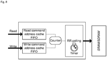
- each BC is connected with an FIFO; a read FIFO and a write FIFO are separately set to execute a read instruction or a write instruction so that a read channel is separated from a write channel; the read FIFO and the write FIFO are polled by a polling device; if there are a predetermined number of read instructions or write instructions in the polled FIFO, the polling device makes the polled FIFO execute the predetermined number of read instructions or write instructions at a time; if there is data needed to be processed in the polled FIFO while the number of the read instructions or write instructions accumulated within a preset period of time fails to reach a predetermined number, the polling device forces the polled FIFO to execute existing read instructions or write instructions at a time.
- the MCT includes: a Group Read/Write Order device GROUP configured to generate a write instruction according to a write request sent from the IPC and the currently idle cache address maintained by the PMG and execute the generated write instruction, generate a read instruction according to a read request sent from the OPC and execute the generated read instruction, and generate a read instruction according to a read request sent from an external application layer of the system and execute the generated read instruction; and an output channel mode selection device configured to select a data output channel, wherein the GROUP outputs the data read from the cache to the OPC or the external application layer of the system according to the output channel selected by the output channel mode selection device.
- GROUP Group Read/Write Order device
- the PMG maintains cache addresses according to a group data cache region and acquires an idle cache address through interleaving access, wherein after a first group of data cache regions are accessed, the other regions excluding the first group of data cache regions are accessed during a second access, and the first group of data cache regions are accessed again only when there is no idle cache address in the other regions excluding the first group of data cache regions; likewise, the other regions excluding the second group of data cache regions are accessed during a third access, and the second group of data cache regions are accessed again only when there is no idle cache address in the other regions excluding the second group of data cache regions; and if no idle cache address is found after each group of data cache regions are traversed, the current write operation is given up to discard data and not resumed unless there is an idle cache address available.
- the group data cache region groups are corresponding to a group of Bank addresses of the cache, wherein a first Bank is precharged after the first Bank is accessed and before the first Bank is accessed again.
- a data caching method for an Ethernet device includes: S101: receiving data frames from various Ethernet interfaces and converting the Ethernet data frames received from the Ethernet interfaces into data frames having a uniform bit width and a uniform encapsulation format; S102: maintaining a cache address in which data has already been written and a currently idle cache address in a cache; S103: receiving the currently idle cache address and generating a write instruction and/or a read instruction for the cache, and performing a write operation and/or a read operation so as to write the data received and processed by an IPC into a currently idle cache or to read data from the cache, wherein the read instruction and/or the write instruction are/is based on an internal read request and/or an internal write request of the system or are/is generated according to a read request received from the outside of the system; and S104: performing bit conversion and format encapsulation on the data that is read according to the read request and outputting the data subjected to the bit conversion
- the algorithm for the scheduling is based on a ROUND-ROBIN polling algorithm or a weighted ROUND-ROBIN polling algorithm.
- Step S103 the generated read instructions or write instructions are accumulated, and when the generated read instructions or write instructions are accumulated to a predetermined number, the accumulated read instructions or write instructions are executed at a time; if the number of the read instructions or write instruction accumulated within a given period of time fails to reach the predetermined number, the accumulated read instructions or write instructions are executed at a time.
- the group data cache region corresponds to a group of Bank addresses of the cache, wherein a first Bank is precharged after the first Bank is accessed and before the first Bank is accessed again.
- the method and the system provided herein are supportive to a plurality of Ethernet interfaces such as XGMII, XLGMII and CGMII as well as a Bypass mode and an Applicant Mode and can be flexibly applied to a fast switching network and a traffic management network to overcome the low efficiency of SDRAM.
- the system and the method provided herein with high expandability improve the expandability and the high bandwidth storage capacity of a network switching device, realize a high bandwidth utilization rate and make it possible to improve bandwidth utilization rate based on traffic management.
- the present disclosure directly realizes the Bank interleaving of an SDRAM in a write direction through cache address management and optimizes the input Bank addresses by re-sorting the Bank addresses in a read direction, thus minimizing the utilization rate consumption of a cache bus operation caused by an overhead time.
- Fig. 1 is a block diagram illustrating the structure of a universal data caching system according to an embodiment of the present disclosure, specifically, the universal data caching system includes:
- a universal data caching method is also provided in an embodiment of the present disclosure which, as shown in Fig. 2 , specifically includes the following steps:
- Step S102 BC ports currently needing to send data are scheduled using an SCH to select a BC port for sending data, the data subjected to the bit conversion and the format conversion is acquired from the BC port and sent to an FIFO to be read so as to write needed data into an SRAM/SDRAM cache.
- the algorithm for the scheduling may be based on ROUND-ROBIN or weighted ROUND-ROBIN, and the ROUND-ROBIN and the weighted ROUND-ROBIN may be switched through a configuration.
- Step S103 the PMG acquires a cache address into which data can be currently written and then sends the cache address to a GROUP device, in this step, a data frame for which no cache address is provided for writing is discarded.
- Step S104 the GROUP device acquires the cache address sent from the PMG, receives cache data needing reading and a corresponding cache address from the inside or the outside of the whole system and generates a write command or a read command.
- the GROUP device adjusts the read/write command and, after a predetermined number of read/write commands are accumulated, sends the read/write commands at a time for continuous reading or writing; if the number of the accumulated commands cannot reach the predetermined number, then a counter counting within a given period of time is set so that the accumulated commands are sent at a time for continuous reading or writing when the value counted by the counter is reached, wherein the number of the continuously read/written commands and a timer are both configurable.
- Step S105 Ethernet data output from the GROUP device is received, subjected to bit conversion in each independent BC inverter, encapsulated and then output from Ethernet interfaces corresponding to bit widths;
- the universal data caching system and method provided herein supportive to various Ethernet interfaces such as XGMII, XLGMII and CGMII are highly expandable and capable of reading or writing data continuously, besides, the system and method achieve a high cache read/write command operation efficiency and can be directly applied to an FPGA or ASIC as needed to improve the expandability and the high bandwidth storage capacity of a network switching device.
- the data caching method provided herein is described below by taking data of a 10G Ethernet as an example.
- the clock frequency is 156.25MHz
- the data width of the XGMII interface is 64 bits and the control data width of the XGMII interface is 8 bits, at the same clock frequency, the data width, the control data width and the clock frequency of the Ethernet data of a 40G XLGMII interface are all four times higher than those of data of a 10G Ethernet;
- the data width of a 100G CGMII interface is 640 bits, and the control data width of the 100G CGMII interface is 80 bits.
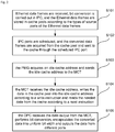
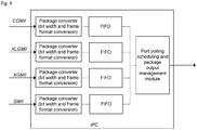
- Fig. 3 is a diagram illustrating the overall framework of the embodiment, and the data caching method specifically includes the following steps: Step 1: an IPC receives a package, the data and related control information sent from a port are subjected to bit conversion and frame format conversion first, a BC supporting an Ethernet MAC data frame format conversion from 32 bits to 640 bits is configured for each high-speed interface.
- the bit widths of different interfaces are uniformly converted to the internal bit width of a device and a format encapsulation operation is implemented.
- the format is encapsulated according to that a frame head is SOP and a frame end is EOP.
- the number of the BCs supportable ranges from 1 to 32, and the input bit width supported by each interface changes from 32 bits to 640 bits, and the supported internal bit supported also changes from 32 bits to 640 bits.
- Step 2 the converted port data and the related control information are stored in an FIFO, the FIFO of each port is independent, and as shown in Fig. 4 , each converter is connected with an FIFO, and the converted Ethernet data is written into an FIFO.
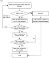
- Fig. 5 which illustrates the flow of the writing of BC port data into an FIFO
- the writing of BC port data into an FIFO is started when the frame head SOP of a package is detected if there is enough space in the FIFO, the package sent from a port will not be written into a data FIFO any more after the FIFO is fully written; if the last package is not completely stored in a data FIFO yet when the FIFO is full, then the package is processed as an error; if the last package is stored at the end of a data frame when an FIFO is full, then an application for polling the FIFO port is sent, after a package output opportunity is gotten through the scheduling of an SCH, the data is sent to the SCH and sequentially sent to the PMG.
- the FULL state cannot be released unless the residual space of the package FIFO is larger than a predetermined number of bits (e.g. 64 bits).
- the bit width of the FIFO is that output by the BC, and the set depth of the FIFO should guarantee the caching of the maximum traffic impact from the interface within the processing delay of a data message on the condition that a data channel suffers no backpressure.
- Step 3 the SCH schedules ports having data waiting to be sent according to the states of data FIFOs and selects a port for sending data.
- the PMG Before data is sent, it is checked whether or not the PMG has an idle address for writing data, if so, data is sent from an SDRAM/SRAM to the SCH through the selected port by taking a data block of a size of given bits as a unit, and the SCH transmits the data to the PMG.
- the end of a package consists of data smaller in size than a data block, then the package is transmitted in its actual size.
- the SCH stops responding to data sending requests of the port FIFOs after completing the current data block transmission until the backpressure signal of the PMG is cleared.
- the SCH schedules the port Ethernet data waiting to be sent using a ROUND-ROBIN or Weighted ROUND-ROBIN polling method.
- the port currently having data is served first; if there are a plurality of ports having data for sending, then the plurality of ports are served in a ROUND-ROBIN manner by taking a data block as a unit.
- the ROUND-ROBIN polling method is mainly applied in a scenario where the internal bandwidth of a system is smaller than the sum of the bandwidths of all input ports, and some ports can be selectively abandoned at an input port in the weighted ROUND-ROBIN polling mode.
- the PMG manages the data cache regions according to cache units which are fixedly distributed according to the biggest package supported by the system. As shown in Fig. 6 , the maximum Ethernet data package size is 2048 bytes, thus, the maximum package size of the cache units is set to be 2048 bytes, the total size of all the cache units is corresponding to the total size of SDRAM/SRAM caches. In the initial state of the system, all the data cache regions internally managed by the PMG are distributable state.
- the cache distribution process of the PMG is as follows: after receiving a data write request from the IPC, the PMG checks whether or not the currently idle cache region can provide enough space for new data to write in, if so, distributes an idle cache region for data writing and internally marks the status bit of the cache unit as 'used'.
- the PMG directly transmits the storage address corresponding to the package, the size of the package, Ethernet type and other related information, to the OPC through the MCT, after processing the related information, the OPC reads data from a corresponding cache address of the MCT, after the data is read, the PGM recovers a corresponding cache address and internally marks the cache unit as 'idle' for the next distribution;
- the PMG directly transmits the storage address corresponding to the package, the size of the package, Ethernet type and other related information to an external application through the MCT, the external application performs a QoS processing on the related information of the package and then returns OPC description information, and similarly, after the OPC reads data from the MCT, the PMG recovers a corresponding cache address and internally marks the cache unit as 'idle' for the next distribution, then the read operation and the recovery of a cache address are completed.
- the data cache regions managed by the PMG are classified based on the features of SDRAMs. It is well known that the low efficiency of DDR SDRAM is due to the overheads caused by the dynamic refresh mechanism of DDR SDRAM, wherein the main overheads are as follows:
- a DDR SDRAM also requires a time interval for the switching from a read operation to a write operation and a time interval for the switching from a write operation to a read operation, the two time intervals are tRWT (Read to Write) which is generally 5-6 clock periods and tWTR (Write to Read) which is generally 4 clock periods; because of the characteristics of the write data of the DDR SDRAM, a read command cannot be sent unless a delay elapses from the completion of the writing of all write data into a data line, thus, a read-write conversion operation significantly lowers the efficiency of the DDR SDRAM.
- tRWT Read to Write
- tWTR Write to Read
- the DDR SDRAM needs to close the row already opened in the current Bank, that is, perform a Precharge operation, every time the DDR SDRAM changes a row in the same Bank, then the DDR SDRAM activates the row needing accessing, that is, performs an Active operation, and finally carries out a data read/write operation.
- a given delay that is, tRP
- the tRP of an ordinary SDRAM occupies four clock periods during which no data read/write operation can be performed.
- the bandwidth utilization rates corresponding to burst lengths 2, 4 and 8 are merely 28%, 44% and 61.5%.
- two successive Active operations are required to be performed at a given time interval, that is, at tRC which typically approximates to 15-20 clock periods, thus causing a huge waste of bandwidth utilization rate.
- the foregoing Bank interleaving 1) is completed by the PMG, the forgoing technologies 2) and 3) are completed by the MCT, and the Bank interleaving 1) is completed in the following way:
- the overhead time of BankO can be perfectly hidden as long as the Precharge operation which is performed on the Bank operated in the first read process between two successive ones of the second to the seventh operation enables the rest Banks to be accessed within the overhead time tRC between two successive Active operations aiming at BankO, thus saving a lot of idle waiting periods.
- Step 5 the MTC generates a read/write command and a read/write address regarding the cache and executes the read/write command.
- the MCT receives a cache address from the PMG, a data write request from the IPC, a read request of the OPC in a Bypass mode and a read request input by an external application in an Applicant mode and completes the interaction of the read/write data, the read/write command and the read/write address with the SDRAM/SRAM cache.
- Step 7 the OPC receives the data read from the cache, performs data bit conversion and frame format encapsulation on the data received and sends the data subjected to the data bit conversion and the frame format encapsulation to a high-speed interface.
- the main structure for chip output is as follows: First, bit conversion and frame format conversion are performed on a data block and related control information (SOP and EOP, mainly) sent from the MCT still by using the BC in line with the IPC so that data frames of an internal bit width are converted to bit widths of different interfaces, and the format of the data frame formats is re-encapsulated.
- the format is encapsulated according to a rule that a frame head is Start Of Package (SOP) and a frame end is End Of Package (EOP).
- the OPC sets a large FIFO for each externally connected high-speed interface to cache the package subjected to the bit and frame format conversion, and after a complete package is cached in the FIFO, the data of the package is read from the FIFO and sent to the interface.
- data of a high-speed Ethernet are cached in a plurality of distributed cache pools, a distribution control is performed by a port scheduler, a currently idle cache pool address is preferably selected after the scheduling to write data into the cache pool of an SDRAM; a device can read a package from the cache pool of the SDRAM automatically or receive an external request concerning the special reading of the currently stored data and then read a package, sequentially process an Ethernet package output from the cache and output the processed Ethernet package to a high-speed interface, thereby realizing the caching-forwarding of Ethernet data in the device.
Landscapes
- Engineering & Computer Science (AREA)
- Computer Networks & Wireless Communication (AREA)
- Signal Processing (AREA)
- Data Exchanges In Wide-Area Networks (AREA)
- Memory System Of A Hierarchy Structure (AREA)
Claims (10)
- Système de mise en mémoire cache de données pour un dispositif Ethernet, dans lequel le système de mise en mémoire cache de données comprend :un dispositif de procédé de paquet d'entrée, IPC (101), configuré pour recevoir des trames de données en provenance de diverses interfaces Ethernet, et convertir les trames de données reçues en provenance des interfaces Ethernet en trames de données ayant une largeur de bit uniforme et un format d'encapsulation uniforme ;un dispositif de gestion d'adresse de paquet, PMG (102), configuré pour conserver une adresse de mémoire cache dans laquelle des données ont déjà été écrites et une adresse de mémoire cache actuellement inactive dans une mémoire cache ;un dispositif de commande de mémoire, MCT, (103), configuré pourrecevoir l'adresse de mémoire cache actuellement inactive en provenance du PMG, générer une instruction d'écriture pour la mémoire cache, et réaliser une opération d'écriture pour écrire les données reçues et traitées par l'IPC dans une mémoire cache actuellement inactive, dans lequel l'instruction d'écriture est basée sur une demande d'écriture interne du système,recevoir l'adresse de mémoire cache en provenance du PMG, générer une instruction de lecture pour la mémoire cache, et réaliser une opération de lecture pour lire des données depuis la mémoire cache, dans lequel l'instruction de lecture est basée sur une demande de lecture interne ou est générée selon une demande de lecture reçue en provenance de l'extérieur du système ; etun dispositif de procédé de paquet de sortie, OPC (104), configuré pour réaliser une conversion de bit et une encapsulation de format sur les données qui sont lues par le MCT sur la base de la demande de lecture, et fournir en sortie les données soumises à la conversion de bit et à l'encapsulation de format par le biais d'une interface Ethernet correspondante ;le système de mise en mémoire cache de données étant caractérisé en ce quele PMG (102) est en outre configuré pour conserver des adresses de mémoire cache selon une région de mémoire cache de données de groupe et acquérir une adresse de mémoire cache inactive par un accès d'entrelacement, dans lequel après accès à un premier groupe de régions de mémoire cache de données, on accède aux autres régions à l'exclusion du premier groupe de régions de mémoire cache de données durant un deuxième accès, et on accède à nouveau au premier groupe de régions de mémoire cache de données uniquement lorsqu'il n'y a pas d'adresse de mémoire cache inactive dans les autres régions à l'exclusion du premier groupe de régions de mémoire cache de données ; de même, on accède aux autres régions à l'exclusion d'un deuxième groupe de régions de mémoire cache de données durant un troisième accès, et on accède à nouveau au deuxième groupe de régions de mémoire cache de données uniquement lorsqu'il n'y a pas d'adresse de mémoire cache inactive dans les autres régions à l'exclusion du deuxième groupe de régions de mémoire cache de données ; et si aucune adresse de mémoire cache inactive n'est trouvée après traversée de chaque groupe de régions de mémoire cache de données, l'opération d'écriture actuelle est abandonnée pour rejeter des données et n'est pas reprise à moins qu'il y ait une adresse de mémoire cache inactive disponible, eten ce que la région de mémoire cache de données de groupe correspond à un groupe d'adresses de banque de la mémoire cache, dans lequel une première banque est préchargée après accès à la première banque et avant accès à nouveau à la première banque.
- Système de mise en mémoire cache de données selon la revendication 1, dans lequel l'IPC (101) comprend une pluralité de convertisseurs de bit, BC, et un ordonnanceur de port, SCH, dans lequel
le BC est configuré pour recevoir des trames de données en provenance d'un type d'interfaces Ethernet et convertir indépendamment les trames de données Ethernet reçues en trames de données ayant une largeur de bit uniforme et un format d'encapsulation uniforme ; et
l'ordonnanceur de port SCH est configuré pour réaliser une opération d'ordonnancement selon une demande d'envoi de données de chaque BC, et envoyer, en prenant un bloc de données d'une taille d'octets fixes en tant qu'unité, les données soumises à la conversion de bit et à l'encapsulation de format dans la pluralité de BC à la mémoire cache dans une séquence d'ordonnancement. - Système de mise en mémoire cache de données selon la revendication 2, dans lequel
le BC est connecté à une file, FIFO ;
une FIFO de lecture et une FIFO d'écriture sont réglées séparément pour exécuter une instruction de lecture ou une instruction d'écriture de sorte qu'un canal de lecture soit séparé d'un canal d'écriture ; la FIFO de lecture et la FIFO d'écriture sont interrogées par un dispositif d'interrogation ; s'il y a un nombre prédéterminé d'instructions de lecture ou d'instructions d'écriture dans la FIFO interrogée, le dispositif d'interrogation amène la FIFO interrogée à exécuter le nombre prédéterminé d'instructions de lecture ou d'instructions d'écriture une par une ; s'il y a des données devant être traitées dans la FIFO interrogée tandis que le nombre des instructions de lecture ou des instructions d'écriture accumulées dans une période de temps préétablie ne parvient pas à atteindre un nombre prédéterminé, le dispositif d'interrogation force la FIFO interrogée à exécuter des instructions de lecture ou des instructions d'écriture existantes une par une. - Système de mise en mémoire cache de données selon la revendication 1, dans lequel le MCT (103) comprend :un dispositif d'ordre de lecture/d'écriture de groupe, GROUP, configuré pour générer une instruction d'écriture selon une demande d'écriture envoyée par l'IPC et l'adresse de mémoire cache actuellement inactive conservée par le PMG, et exécuter l'instruction d'écriture générée ; générer une instruction de lecture selon une demande de lecture envoyée par l'OPC et exécuter l'instruction de lecture générée ; générer une instruction de lecture selon une demande de lecture envoyée par une couche d'application externe du système et exécuter l'instruction de lecture générée ; et fournir en sortie les données lues depuis la mémoire cache à l'OPC ou la couche d'application externe du système selon un canal de sortie choisi par un dispositif de sélection de mode de canal de sortie ;le dispositif de sélection de mode de canal de sortie est configuré pour sélectionner le canal de sortie de données.
- Système de mise en mémoire cache de données selon la revendication 1, dans lequel lorsqu'une pluralité d'instructions de lecture est générée par le MCT, la pluralité d'instructions de lecture est triée de sorte que les instructions de lecture correspondant à des adresses de mémoire cache lues de manière entrelacée soient placées à l'avant pour exécuter une opération de lecture, et des données sont triées à nouveau dans une séquence souhaitée par l'intérieur ou l'extérieur du système puis fournies en sortie.
- Procédé de mise en mémoire cache de données pour un dispositif Ethernet, dans lequel le procédé de mise en mémoire cache de données comprend les étapes suivantes :(S101) au niveau d'un dispositif de procédé de paquet d'entrée, IPC (101), la réception de trames de données en provenance de diverses interfaces Ethernet et la conversion des trames de données Ethernet reçues en provenance des interfaces Ethernet en trames de données ayant une largeur de bit uniforme et un format d'encapsulation uniforme ;(S102) la conservation d'une adresse de mémoire cache dans laquelle des données ont déjà été écrites et d'une adresse de mémoire cache actuellement inactive dans une mémoire cache ;(S103) la réception de l'adresse de mémoire cache actuellement inactive et la génération d'une instruction d'écriture pour la mémoire cache, et la réalisation d'une opération d'écriture de façon à écrire les données reçues et traitées par l'IPC dans une mémoire cache actuellement inactive, dans lequel l'instruction d'écriture est basée sur une demande d'écriture interne du système,la réception de l'adresse de mémoire cache et la génération d'une instruction de lecture pour la mémoire cache, et la réalisation d'une opération de lecture de façon à lire des données depuis la mémoire cache, dans lequel l'instruction de lecture est basée sur une demande de lecture interne du système ou est générée selon une demande de lecture reçue en provenance de l'extérieur du système ; et(5104) la réalisation d'une conversion de bit et d'un format d'encapsulation sur les données qui sont lues selon la demande de lecture et la fourniture en sortie des données soumises à la conversion de bit et à l'encapsulation de format par le biais d'une interface Ethernet correspondante,le procédé de mise en mémoire cache de données étant caractérisé en ce queà l'étape de conservation d'une adresse de mémoire cache, la maintenance fait référence à la maintenance d'adresses de mémoire cache selon une région de mémoire cache de données de groupe, et l'adresse de mémoire cache inactive est acquise par un accès d'entrelacement, dans lequel après accès à un premier groupe de régions de mémoire cache de données, on accède aux autres régions à l'exclusion du premier groupe de régions de mémoire cache de données durant un deuxième accès, et on accède à nouveau au premier groupe de régions de mémoire cache de données uniquement lorsqu'il n'y a pas d'adresse de mémoire cache inactive dans les autres régions à l'exclusion du premier groupe de régions de mémoire cache de données ; de même, on accède aux autres régions à l'exclusion d'un deuxième groupe de régions de mémoire cache de données durant un troisième accès, et on accède à nouveau au deuxième groupe de régions de mémoire cache de données uniquement lorsqu'il n'y a pas d'adresse de mémoire cache inactive dans les autres régions à l'exclusion du deuxième groupe de régions de mémoire cache de données ; et si aucune adresse de mémoire cache inactive n'est trouvée après traversée de chaque groupe de régions de mémoire cache de données, l'opération d'écriture actuelle est abandonnée pour rejeter des données et n'est pas reprise à moins qu'il y ait une adresse de mémoire cache inactive disponible, eten ce que la région de mémoire cache de données de groupe correspond à un groupe d'adresses de banque de la mémoire cache, dans laquelle une première banque est préchargée après accès à la première banque et avant accès à nouveau à la première banque.
- Procédé de mise en mémoire cache de données selon la revendication 6, dans lequel à l'étape de réception et de conversion des trames de données Ethernet, les données soumises à la conversion de bit et à l'encapsulation de format sont ordonnancées pour être envoyées séquentiellement à la mémoire cache dans une séquence d'ordonnancement en prenant un bloc de données d'une taille d'octets fixes en tant qu'unité.
- Procédé de mise en mémoire cache de données selon la revendication 7, dans lequel l'algorithme pour l'ordonnancement est basé sur un algorithme d'interrogation de circuit cyclique ou un algorithme d'interrogation de circuit cyclique pondéré.
- Procédé de mise en mémoire cache de données selon la revendication 6, dans lequel à l'étape de génération d'une instruction d'écriture et d'une instruction de lecture pour la mémoire cache, les instructions de lecture ou les instructions d'écriture générées sont accumulées, et lorsque les instructions de lecture ou les instructions d'écriture générées sont accumulées jusqu'à un nombre prédéterminé, les instructions de lecture ou les instructions d'écriture accumulées sont exécutées une par une ; si le nombre des instructions de lecture ou des instructions d'écriture accumulées dans une période de temps donnée ne parvient pas à atteindre le nombre prédéterminé, les instructions de lecture ou les instructions d'écriture accumulées sont exécutées une par une.
- Procédé de mise en mémoire cache de données selon la revendication 6, dans lequel lorsqu'une pluralité d'instructions de lecture est générée, la pluralité d'instructions de lecture est triée de sorte que des instructions de lecture correspondant à des adresses de mémoire cache lues de manière entrelacée soient placées à l'avant pour exécuter une opération de lecture, et des données sont triées à nouveau dans une séquence souhaitée par l'intérieur ou l'extérieur du système puis fournies en sortie.
Applications Claiming Priority (2)
| Application Number | Priority Date | Filing Date | Title |
|---|---|---|---|
| CN201210415255.5A CN103780506B (zh) | 2012-10-26 | 2012-10-26 | 一种用于以太网设备的数据缓存系统及方法 |
| PCT/CN2013/085607 WO2014063599A1 (fr) | 2012-10-26 | 2013-10-21 | Système et procédé de mise en tampon de données pour un dispositif ethernet |
Publications (3)
| Publication Number | Publication Date |
|---|---|
| EP2913963A1 EP2913963A1 (fr) | 2015-09-02 |
| EP2913963A4 EP2913963A4 (fr) | 2015-10-28 |
| EP2913963B1 true EP2913963B1 (fr) | 2018-08-29 |
Family
ID=50544012
Family Applications (1)
| Application Number | Title | Priority Date | Filing Date |
|---|---|---|---|
| EP13849347.3A Active EP2913963B1 (fr) | 2012-10-26 | 2013-10-21 | Système et procédé de mise en cache de données pour un dispositif ethernet |
Country Status (4)
| Country | Link |
|---|---|
| US (1) | US9712461B2 (fr) |
| EP (1) | EP2913963B1 (fr) |
| CN (1) | CN103780506B (fr) |
| WO (1) | WO2014063599A1 (fr) |
Families Citing this family (32)
| Publication number | Priority date | Publication date | Assignee | Title |
|---|---|---|---|---|
| CN105630825B (zh) * | 2014-11-04 | 2021-04-06 | 中兴通讯股份有限公司 | 一种数据转换方法及装置 |
| CN105573922B (zh) * | 2014-11-07 | 2020-07-10 | 中兴通讯股份有限公司 | 一种实现数据格式转换的方法和装置 |
| CN105681904A (zh) * | 2016-01-18 | 2016-06-15 | 四川长虹电器股份有限公司 | 提高电视响应速度的方法 |
| CN105912479B (zh) * | 2016-04-07 | 2023-05-05 | 合肥锐世数字科技有限公司 | 一种并发数据的缓存方法及装置 |
| CN107809395B (zh) * | 2017-10-11 | 2019-12-10 | 大唐恩智浦半导体有限公司 | 一种电池管理系统的通信方法及电池管理系统 |
| CN108234266B (zh) * | 2018-01-22 | 2020-08-21 | 珠海格力电器股份有限公司 | 总线型通讯网络的数据传输方法和装置及存储介质 |
| CN110012367B (zh) * | 2019-03-27 | 2021-10-19 | 烽火通信科技股份有限公司 | 用于gpon olt的omci组帧装置及组帧方法 |
| CN110996057B (zh) * | 2019-12-02 | 2021-11-16 | 腾讯云计算(北京)有限责任公司 | 媒体数据处理方法、装置、计算机设备和存储介质 |
| CN113535633B (zh) * | 2020-04-17 | 2025-07-29 | 深圳市中兴微电子技术有限公司 | 一种片上缓存装置和读写方法 |
| CN112073316B (zh) * | 2020-09-09 | 2022-08-26 | 南京盛科通信有限公司 | 多通道位宽变化的数据传输系统、方法、设备和存储介质 |
| CN112905150A (zh) * | 2021-02-18 | 2021-06-04 | 袁本翔 | 一种基于异步fifo芯片的处理电路及可重构工作方法 |
| CN113109778B (zh) * | 2021-02-26 | 2023-06-30 | 西安电子科技大学 | 一种基于中断响应机制的多体制雷达预处理实现方法 |
| CN115206362A (zh) | 2021-04-13 | 2022-10-18 | 长鑫存储技术有限公司 | 数据传输电路、方法及存储装置 |
| US11810637B2 (en) | 2021-04-13 | 2023-11-07 | Changxin Memory Technologies, Inc. | Data transmission circuit, data transmission method, and storage apparatus with read-write conversion circuit |
| CN115206361B (zh) * | 2021-04-13 | 2025-06-27 | 长鑫存储技术有限公司 | 数据传输电路、方法及存储装置 |
| US11901028B2 (en) | 2021-04-13 | 2024-02-13 | Changxin Memory Technologies, Inc. | Data transmission circuit, data transmission method, and storage apparatus |
| CN113672169A (zh) * | 2021-07-19 | 2021-11-19 | 浙江大华技术股份有限公司 | 流处理系统的数据读写方法和流处理系统 |
| CN113824649B (zh) * | 2021-09-17 | 2023-10-27 | 上海航天计算机技术研究所 | 面向固定帧长的数据流量控制装置 |
| CN113873251B (zh) * | 2021-10-12 | 2024-11-01 | 上海航天测控通信研究所 | 一种地址分区管理的多通道全色多光谱图像压缩调度方法 |
| CN113934378B (zh) * | 2021-11-01 | 2024-04-19 | 新华三技术有限公司合肥分公司 | 一种数据缓存方法、逻辑装置和电子设备 |
| CN114741331B (zh) * | 2022-04-01 | 2025-11-04 | 深圳云豹智能股份有限公司 | 一种数据缓存装置、系统及数据处理方法 |
| CN115378887B (zh) * | 2022-07-05 | 2024-01-23 | 西安电子科技大学 | 一种时间触发以太网交换机tt业务交换装置 |
| CN117560359B (zh) * | 2022-08-03 | 2025-12-19 | 深圳市中兴微电子技术有限公司 | DigRF帧处理方法、装置、计算机设备及可读介质 |
| CN115297094B (zh) * | 2022-10-08 | 2023-02-28 | 苏州浪潮智能科技有限公司 | 视频传输控制方法、装置、设备及计算机可读存储介质 |
| CN116074406B (zh) * | 2022-11-29 | 2024-07-19 | 北京华峰装备技术有限公司 | 指令发送方法及装置 |
| CN115904246A (zh) * | 2022-12-22 | 2023-04-04 | 北京天融信网络安全技术有限公司 | 一种基于多路ddr内存的数据读取方法及装置 |
| KR20240170170A (ko) * | 2023-05-26 | 2024-12-03 | 에스케이하이닉스 주식회사 | 별개의 커맨드들을 병합한 커맨드를 처리하는 스토리지 컨트롤러를 포함하는 스토리지 장치 및 이의 동작 방법 |
| CN116893983B (zh) * | 2023-09-11 | 2023-12-12 | 中移(苏州)软件技术有限公司 | 数据缓存方法、设备及介质 |
| CN117725002B (zh) * | 2023-12-12 | 2025-09-30 | 海光信息技术股份有限公司 | 数据传输方法、数据传输装置和电子设备 |
| CN117640783B (zh) * | 2024-01-25 | 2024-04-09 | 富瀚微电子(成都)有限公司 | 一种数据传输方法、系统、电子设备以及可读介质 |
| CN118473601B (zh) * | 2024-07-09 | 2024-10-11 | 成都态坦测试科技有限公司 | 一种复用组帧方法、装置及终端设备 |
| CN120282050B (zh) * | 2025-06-10 | 2025-08-19 | 杭州芯旗电子技术有限公司 | 基于fpga的细颗粒光传送网的开销处理装置及方法 |
Citations (1)
| Publication number | Priority date | Publication date | Assignee | Title |
|---|---|---|---|---|
| CN102629914A (zh) * | 2012-04-27 | 2012-08-08 | 深圳市邦彦信息技术有限公司 | 一种以太网数据包缓存方法和装置 |
Family Cites Families (10)
| Publication number | Priority date | Publication date | Assignee | Title |
|---|---|---|---|---|
| US6771646B1 (en) * | 1999-06-30 | 2004-08-03 | Hi/Fn, Inc. | Associative cache structure for lookups and updates of flow records in a network monitor |
| US6865189B2 (en) * | 2001-03-22 | 2005-03-08 | Lsi Logic Corporation | Minimal latency serial media independent interface to media independent interface converter |
| CN1221104C (zh) * | 2002-07-12 | 2005-09-28 | 华为技术有限公司 | 一种利用帧定位实现包方式数据高位宽到低位宽的格式转换方法 |
| CN100466601C (zh) * | 2005-04-28 | 2009-03-04 | 华为技术有限公司 | 一种数据读写装置及其读写方法 |
| CN100571195C (zh) * | 2005-07-27 | 2009-12-16 | 华为技术有限公司 | 多端口以太网交换装置及数据传输方法 |
| CN201118640Y (zh) * | 2007-07-20 | 2008-09-17 | 核工业理化工程研究院 | 多接口通讯协议转换器 |
| CN101146091B (zh) * | 2007-09-05 | 2010-09-08 | 中兴通讯股份有限公司 | 多通道数据输出方法及系统 |
| CN101567845B (zh) * | 2009-04-27 | 2011-12-07 | 成都科来软件有限公司 | 一种通用网络数据包实时处理系统及方法 |
| US8499137B2 (en) * | 2010-03-12 | 2013-07-30 | Lsi Corporation | Memory manager for a network communications processor architecture |
| US9319348B2 (en) * | 2011-05-24 | 2016-04-19 | Cisco Technology, Inc. | Octal serial gigabit media-independent interface |
-
2012
- 2012-10-26 CN CN201210415255.5A patent/CN103780506B/zh active Active
-
2013
- 2013-10-21 US US14/437,904 patent/US9712461B2/en active Active
- 2013-10-21 EP EP13849347.3A patent/EP2913963B1/fr active Active
- 2013-10-21 WO PCT/CN2013/085607 patent/WO2014063599A1/fr not_active Ceased
Patent Citations (1)
| Publication number | Priority date | Publication date | Assignee | Title |
|---|---|---|---|---|
| CN102629914A (zh) * | 2012-04-27 | 2012-08-08 | 深圳市邦彦信息技术有限公司 | 一种以太网数据包缓存方法和装置 |
Also Published As
| Publication number | Publication date |
|---|---|
| CN103780506B (zh) | 2017-08-08 |
| CN103780506A (zh) | 2014-05-07 |
| US20150295859A1 (en) | 2015-10-15 |
| EP2913963A1 (fr) | 2015-09-02 |
| US9712461B2 (en) | 2017-07-18 |
| WO2014063599A1 (fr) | 2014-05-01 |
| EP2913963A4 (fr) | 2015-10-28 |
Similar Documents
| Publication | Publication Date | Title |
|---|---|---|
| EP2913963B1 (fr) | Système et procédé de mise en cache de données pour un dispositif ethernet | |
| US8225026B2 (en) | Data packet access control apparatus and method thereof | |
| US9870327B2 (en) | Message-based memory access apparatus and access method thereof | |
| CN102684976B (zh) | 一种基于ddr sdram进行数据读写的方法、装置及系统 | |
| EP3657744B1 (fr) | Traitement de message | |
| CN101222444B (zh) | 缓存数据处理方法、装置及系统 | |
| US8886741B2 (en) | Receive queue models to reduce I/O cache consumption | |
| GB2388216A (en) | Multi-bank scheduling to improve performance on tree access in a dram based RAM subsystem | |
| US7822915B2 (en) | Memory controller for packet applications | |
| EP3166269B1 (fr) | Procédé et appareil de gestion de file d'attente | |
| TWI301367B (en) | Compact packet switching node storage architecture employing double data rate synchronous dynamic ram | |
| CN113821457B (zh) | 一种高性能读写链表缓存的装置及方法 | |
| CN100466601C (zh) | 一种数据读写装置及其读写方法 | |
| US20150006828A1 (en) | Memory architecture determining the number of replicas stored in memory banks or devices according to a packet size | |
| CN101656586B (zh) | 提高同步数字体系虚级联延时补偿缓存效率的方法及装置 | |
| CN102439534A (zh) | 降低数据类芯片外挂ddr功耗的方法及数据类芯片系统 | |
| US10031884B2 (en) | Storage apparatus and method for processing plurality of pieces of client data | |
| CN102571535B (zh) | 一种数据延迟装置、方法及通信系统 | |
| US7127547B2 (en) | Processor with multiple linked list storage feature | |
| CN102833145A (zh) | 一种自适应动态调整带宽的装置及方法 | |
| US8572349B2 (en) | Processor with programmable configuration of logical-to-physical address translation on a per-client basis | |
| WO2020219293A1 (fr) | Partitionnement de contrôleur de mémoire pour système de mémoire hybride | |
| WO2019120274A1 (fr) | Procédé et appareil de mémoire tampon circulaire de données pour socfpga, support de stockage et terminal | |
| CN120336254A (zh) | 一种基于fpga的多通道ddr4存储装置 | |
| Priyanka et al. | AMBA AXI COMPLIANT DMA CONTROLLER FOR EFFICIENT DATA TRANSFER |
Legal Events
| Date | Code | Title | Description |
|---|---|---|---|
| PUAI | Public reference made under article 153(3) epc to a published international application that has entered the european phase |
Free format text: ORIGINAL CODE: 0009012 |
|
| 17P | Request for examination filed |
Effective date: 20150507 |
|
| AK | Designated contracting states |
Kind code of ref document: A1 Designated state(s): AL AT BE BG CH CY CZ DE DK EE ES FI FR GB GR HR HU IE IS IT LI LT LU LV MC MK MT NL NO PL PT RO RS SE SI SK SM TR |
|
| AX | Request for extension of the european patent |
Extension state: BA ME |
|
| RA4 | Supplementary search report drawn up and despatched (corrected) |
Effective date: 20150929 |
|
| RIC1 | Information provided on ipc code assigned before grant |
Ipc: H04L 12/70 20130101AFI20150923BHEP Ipc: H04L 12/879 20130101ALI20150923BHEP Ipc: H04L 12/931 20130101ALI20150923BHEP |
|
| DAX | Request for extension of the european patent (deleted) | ||
| REG | Reference to a national code |
Ref country code: DE Ref legal event code: R079 Ref document number: 602013042892 Country of ref document: DE Free format text: PREVIOUS MAIN CLASS: H04L0012700000 Ipc: H04L0029120000 |
|
| GRAP | Despatch of communication of intention to grant a patent |
Free format text: ORIGINAL CODE: EPIDOSNIGR1 |
|
| STAA | Information on the status of an ep patent application or granted ep patent |
Free format text: STATUS: GRANT OF PATENT IS INTENDED |
|
| RIC1 | Information provided on ipc code assigned before grant |
Ipc: H04L 12/879 20130101ALI20180223BHEP Ipc: H04L 12/70 20130101ALI20180223BHEP Ipc: H04L 12/863 20130101ALI20180223BHEP Ipc: H04L 12/931 20130101ALI20180223BHEP Ipc: H04L 29/12 20060101AFI20180223BHEP |
|
| INTG | Intention to grant announced |
Effective date: 20180323 |
|
| GRAS | Grant fee paid |
Free format text: ORIGINAL CODE: EPIDOSNIGR3 |
|
| GRAA | (expected) grant |
Free format text: ORIGINAL CODE: 0009210 |
|
| STAA | Information on the status of an ep patent application or granted ep patent |
Free format text: STATUS: THE PATENT HAS BEEN GRANTED |
|
| AK | Designated contracting states |
Kind code of ref document: B1 Designated state(s): AL AT BE BG CH CY CZ DE DK EE ES FI FR GB GR HR HU IE IS IT LI LT LU LV MC MK MT NL NO PL PT RO RS SE SI SK SM TR |
|
| REG | Reference to a national code |
Ref country code: GB Ref legal event code: FG4D |
|
| REG | Reference to a national code |
Ref country code: CH Ref legal event code: EP |
|
| REG | Reference to a national code |
Ref country code: AT Ref legal event code: REF Ref document number: 1036543 Country of ref document: AT Kind code of ref document: T Effective date: 20180915 |
|
| REG | Reference to a national code |
Ref country code: IE Ref legal event code: FG4D |
|
| REG | Reference to a national code |
Ref country code: DE Ref legal event code: R096 Ref document number: 602013042892 Country of ref document: DE |
|
| REG | Reference to a national code |
Ref country code: FR Ref legal event code: PLFP Year of fee payment: 6 |
|
| REG | Reference to a national code |
Ref country code: NL Ref legal event code: MP Effective date: 20180829 |
|
| REG | Reference to a national code |
Ref country code: LT Ref legal event code: MG4D |
|
| PG25 | Lapsed in a contracting state [announced via postgrant information from national office to epo] |
Ref country code: FI Free format text: LAPSE BECAUSE OF FAILURE TO SUBMIT A TRANSLATION OF THE DESCRIPTION OR TO PAY THE FEE WITHIN THE PRESCRIBED TIME-LIMIT Effective date: 20180829 Ref country code: GR Free format text: LAPSE BECAUSE OF FAILURE TO SUBMIT A TRANSLATION OF THE DESCRIPTION OR TO PAY THE FEE WITHIN THE PRESCRIBED TIME-LIMIT Effective date: 20181130 Ref country code: SE Free format text: LAPSE BECAUSE OF FAILURE TO SUBMIT A TRANSLATION OF THE DESCRIPTION OR TO PAY THE FEE WITHIN THE PRESCRIBED TIME-LIMIT Effective date: 20180829 Ref country code: BG Free format text: LAPSE BECAUSE OF FAILURE TO SUBMIT A TRANSLATION OF THE DESCRIPTION OR TO PAY THE FEE WITHIN THE PRESCRIBED TIME-LIMIT Effective date: 20181129 Ref country code: NL Free format text: LAPSE BECAUSE OF FAILURE TO SUBMIT A TRANSLATION OF THE DESCRIPTION OR TO PAY THE FEE WITHIN THE PRESCRIBED TIME-LIMIT Effective date: 20180829 Ref country code: NO Free format text: LAPSE BECAUSE OF FAILURE TO SUBMIT A TRANSLATION OF THE DESCRIPTION OR TO PAY THE FEE WITHIN THE PRESCRIBED TIME-LIMIT Effective date: 20181129 Ref country code: RS Free format text: LAPSE BECAUSE OF FAILURE TO SUBMIT A TRANSLATION OF THE DESCRIPTION OR TO PAY THE FEE WITHIN THE PRESCRIBED TIME-LIMIT Effective date: 20180829 Ref country code: LT Free format text: LAPSE BECAUSE OF FAILURE TO SUBMIT A TRANSLATION OF THE DESCRIPTION OR TO PAY THE FEE WITHIN THE PRESCRIBED TIME-LIMIT Effective date: 20180829 Ref country code: IS Free format text: LAPSE BECAUSE OF FAILURE TO SUBMIT A TRANSLATION OF THE DESCRIPTION OR TO PAY THE FEE WITHIN THE PRESCRIBED TIME-LIMIT Effective date: 20181229 |
|
| REG | Reference to a national code |
Ref country code: AT Ref legal event code: MK05 Ref document number: 1036543 Country of ref document: AT Kind code of ref document: T Effective date: 20180829 |
|
| PG25 | Lapsed in a contracting state [announced via postgrant information from national office to epo] |
Ref country code: HR Free format text: LAPSE BECAUSE OF FAILURE TO SUBMIT A TRANSLATION OF THE DESCRIPTION OR TO PAY THE FEE WITHIN THE PRESCRIBED TIME-LIMIT Effective date: 20180829 Ref country code: AL Free format text: LAPSE BECAUSE OF FAILURE TO SUBMIT A TRANSLATION OF THE DESCRIPTION OR TO PAY THE FEE WITHIN THE PRESCRIBED TIME-LIMIT Effective date: 20180829 Ref country code: LV Free format text: LAPSE BECAUSE OF FAILURE TO SUBMIT A TRANSLATION OF THE DESCRIPTION OR TO PAY THE FEE WITHIN THE PRESCRIBED TIME-LIMIT Effective date: 20180829 |
|
| PG25 | Lapsed in a contracting state [announced via postgrant information from national office to epo] |
Ref country code: ES Free format text: LAPSE BECAUSE OF FAILURE TO SUBMIT A TRANSLATION OF THE DESCRIPTION OR TO PAY THE FEE WITHIN THE PRESCRIBED TIME-LIMIT Effective date: 20180829 Ref country code: EE Free format text: LAPSE BECAUSE OF FAILURE TO SUBMIT A TRANSLATION OF THE DESCRIPTION OR TO PAY THE FEE WITHIN THE PRESCRIBED TIME-LIMIT Effective date: 20180829 Ref country code: AT Free format text: LAPSE BECAUSE OF FAILURE TO SUBMIT A TRANSLATION OF THE DESCRIPTION OR TO PAY THE FEE WITHIN THE PRESCRIBED TIME-LIMIT Effective date: 20180829 Ref country code: CZ Free format text: LAPSE BECAUSE OF FAILURE TO SUBMIT A TRANSLATION OF THE DESCRIPTION OR TO PAY THE FEE WITHIN THE PRESCRIBED TIME-LIMIT Effective date: 20180829 Ref country code: RO Free format text: LAPSE BECAUSE OF FAILURE TO SUBMIT A TRANSLATION OF THE DESCRIPTION OR TO PAY THE FEE WITHIN THE PRESCRIBED TIME-LIMIT Effective date: 20180829 Ref country code: IT Free format text: LAPSE BECAUSE OF FAILURE TO SUBMIT A TRANSLATION OF THE DESCRIPTION OR TO PAY THE FEE WITHIN THE PRESCRIBED TIME-LIMIT Effective date: 20180829 Ref country code: PL Free format text: LAPSE BECAUSE OF FAILURE TO SUBMIT A TRANSLATION OF THE DESCRIPTION OR TO PAY THE FEE WITHIN THE PRESCRIBED TIME-LIMIT Effective date: 20180829 |
|
| PG25 | Lapsed in a contracting state [announced via postgrant information from national office to epo] |
Ref country code: DK Free format text: LAPSE BECAUSE OF FAILURE TO SUBMIT A TRANSLATION OF THE DESCRIPTION OR TO PAY THE FEE WITHIN THE PRESCRIBED TIME-LIMIT Effective date: 20180829 Ref country code: SK Free format text: LAPSE BECAUSE OF FAILURE TO SUBMIT A TRANSLATION OF THE DESCRIPTION OR TO PAY THE FEE WITHIN THE PRESCRIBED TIME-LIMIT Effective date: 20180829 Ref country code: SM Free format text: LAPSE BECAUSE OF FAILURE TO SUBMIT A TRANSLATION OF THE DESCRIPTION OR TO PAY THE FEE WITHIN THE PRESCRIBED TIME-LIMIT Effective date: 20180829 |
|
| REG | Reference to a national code |
Ref country code: CH Ref legal event code: PL Ref country code: DE Ref legal event code: R097 Ref document number: 602013042892 Country of ref document: DE |
|
| REG | Reference to a national code |
Ref country code: BE Ref legal event code: MM Effective date: 20181031 |
|
| PG25 | Lapsed in a contracting state [announced via postgrant information from national office to epo] |
Ref country code: MC Free format text: LAPSE BECAUSE OF FAILURE TO SUBMIT A TRANSLATION OF THE DESCRIPTION OR TO PAY THE FEE WITHIN THE PRESCRIBED TIME-LIMIT Effective date: 20180829 Ref country code: LU Free format text: LAPSE BECAUSE OF NON-PAYMENT OF DUE FEES Effective date: 20181021 |
|
| PLBE | No opposition filed within time limit |
Free format text: ORIGINAL CODE: 0009261 |
|
| STAA | Information on the status of an ep patent application or granted ep patent |
Free format text: STATUS: NO OPPOSITION FILED WITHIN TIME LIMIT |
|
| REG | Reference to a national code |
Ref country code: IE Ref legal event code: MM4A |
|
| 26N | No opposition filed |
Effective date: 20190531 |
|
| PG25 | Lapsed in a contracting state [announced via postgrant information from national office to epo] |
Ref country code: SI Free format text: LAPSE BECAUSE OF FAILURE TO SUBMIT A TRANSLATION OF THE DESCRIPTION OR TO PAY THE FEE WITHIN THE PRESCRIBED TIME-LIMIT Effective date: 20180829 Ref country code: BE Free format text: LAPSE BECAUSE OF NON-PAYMENT OF DUE FEES Effective date: 20181031 Ref country code: LI Free format text: LAPSE BECAUSE OF NON-PAYMENT OF DUE FEES Effective date: 20181031 Ref country code: CH Free format text: LAPSE BECAUSE OF NON-PAYMENT OF DUE FEES Effective date: 20181031 |
|
| PG25 | Lapsed in a contracting state [announced via postgrant information from national office to epo] |
Ref country code: IE Free format text: LAPSE BECAUSE OF NON-PAYMENT OF DUE FEES Effective date: 20181021 |
|
| PG25 | Lapsed in a contracting state [announced via postgrant information from national office to epo] |
Ref country code: MT Free format text: LAPSE BECAUSE OF NON-PAYMENT OF DUE FEES Effective date: 20181021 |
|
| PG25 | Lapsed in a contracting state [announced via postgrant information from national office to epo] |
Ref country code: TR Free format text: LAPSE BECAUSE OF FAILURE TO SUBMIT A TRANSLATION OF THE DESCRIPTION OR TO PAY THE FEE WITHIN THE PRESCRIBED TIME-LIMIT Effective date: 20180829 |
|
| PG25 | Lapsed in a contracting state [announced via postgrant information from national office to epo] |
Ref country code: PT Free format text: LAPSE BECAUSE OF FAILURE TO SUBMIT A TRANSLATION OF THE DESCRIPTION OR TO PAY THE FEE WITHIN THE PRESCRIBED TIME-LIMIT Effective date: 20180829 |
|
| PG25 | Lapsed in a contracting state [announced via postgrant information from national office to epo] |
Ref country code: MK Free format text: LAPSE BECAUSE OF NON-PAYMENT OF DUE FEES Effective date: 20180829 Ref country code: HU Free format text: LAPSE BECAUSE OF FAILURE TO SUBMIT A TRANSLATION OF THE DESCRIPTION OR TO PAY THE FEE WITHIN THE PRESCRIBED TIME-LIMIT; INVALID AB INITIO Effective date: 20131021 Ref country code: CY Free format text: LAPSE BECAUSE OF FAILURE TO SUBMIT A TRANSLATION OF THE DESCRIPTION OR TO PAY THE FEE WITHIN THE PRESCRIBED TIME-LIMIT Effective date: 20180829 |
|
| REG | Reference to a national code |
Ref country code: DE Ref legal event code: R079 Ref document number: 602013042892 Country of ref document: DE Free format text: PREVIOUS MAIN CLASS: H04L0029120000 Ipc: H04L0067286900 |
|
| REG | Reference to a national code |
Ref country code: DE Ref legal event code: R081 Ref document number: 602013042892 Country of ref document: DE Owner name: SANECHIPS TECHNOLOGY CO., LTD., SHENZHEN, CN Free format text: FORMER OWNER: ZTE CORPORATION, SHENZHEN, GUANGDONG, CN |
|
| REG | Reference to a national code |
Ref country code: GB Ref legal event code: 732E Free format text: REGISTERED BETWEEN 20230406 AND 20230412 |
|
| PGFP | Annual fee paid to national office [announced via postgrant information from national office to epo] |
Ref country code: GB Payment date: 20250904 Year of fee payment: 13 |
|
| PGFP | Annual fee paid to national office [announced via postgrant information from national office to epo] |
Ref country code: FR Payment date: 20250908 Year of fee payment: 13 |
|
| PGFP | Annual fee paid to national office [announced via postgrant information from national office to epo] |
Ref country code: DE Payment date: 20250902 Year of fee payment: 13 |