EP2916618A1 - Dispositif de blindage pour appareil à micro-ondes - Google Patents
Dispositif de blindage pour appareil à micro-ondes Download PDFInfo
- Publication number
- EP2916618A1 EP2916618A1 EP14158172.8A EP14158172A EP2916618A1 EP 2916618 A1 EP2916618 A1 EP 2916618A1 EP 14158172 A EP14158172 A EP 14158172A EP 2916618 A1 EP2916618 A1 EP 2916618A1
- Authority
- EP
- European Patent Office
- Prior art keywords
- gap
- shielding device
- microwave
- shielding
- dielectric
- Prior art date
- Legal status (The legal status is an assumption and is not a legal conclusion. Google has not performed a legal analysis and makes no representation as to the accuracy of the status listed.)
- Granted
Links
Images
Classifications
-
- H—ELECTRICITY
- H05—ELECTRIC TECHNIQUES NOT OTHERWISE PROVIDED FOR
- H05B—ELECTRIC HEATING; ELECTRIC LIGHT SOURCES NOT OTHERWISE PROVIDED FOR; CIRCUIT ARRANGEMENTS FOR ELECTRIC LIGHT SOURCES, IN GENERAL
- H05B6/00—Heating by electric, magnetic or electromagnetic fields
- H05B6/64—Heating using microwaves
- H05B6/78—Arrangements for continuous movement of material
-
- H—ELECTRICITY
- H05—ELECTRIC TECHNIQUES NOT OTHERWISE PROVIDED FOR
- H05B—ELECTRIC HEATING; ELECTRIC LIGHT SOURCES NOT OTHERWISE PROVIDED FOR; CIRCUIT ARRANGEMENTS FOR ELECTRIC LIGHT SOURCES, IN GENERAL
- H05B6/00—Heating by electric, magnetic or electromagnetic fields
- H05B6/64—Heating using microwaves
- H05B6/76—Prevention of microwave leakage, e.g. door sealings
Definitions
- the invention relates to a shielding device for a microwave device for the thermal treatment of products and a microwave device, wherein the shielding device in a microwave shielding wall of the microwave device can be arranged, wherein the shielding device for microwave shielding performing a moving member through the wall, wherein the shielding device comprises the moving element and a passage opening for the moving member is formed, wherein the moving member is for transmitting a movement and is guided through the passage opening, wherein between the passage opening and the moving element, a dielectric gap is formed, wherein a geometric shape of the gap is formed so that the gap forms a band-stop filter for microwaves.
- Microwave ovens are well known in the art and are commonly used for heating or cooking food, as well as in the industrial field for the thermal treatment of products or components. Especially in industrial applications is a power of the microwave oven comparatively high, so it requires an effective shielding of a treatment room of the microwave oven.
- the shielding of the treatment space is formed by a metallic wall of the treatment space. In the region of a door of a treatment room, this can also be provided, for example, with a perforated plate whose hole size is smaller than a wavelength of the microwaves, so that shielding can also be achieved here.
- microwave ovens Due to reflections of the microwaves within the treatment space, a three-dimensional pattern of interference maxima of the microwaves results, which leads to an inhomogeneous heating of the products placed in the treatment space.
- microwave ovens it is therefore customary to use a rotatable plate to achieve a homogeneous heat distribution in the food.
- reflection mirrors are used in microwave ovens, especially in microwave ovens used industrially. Reflecting rotating mirrors have metal reflecting surfaces for microwaves, wherein a homogeneous rotation of the reflecting surfaces causes a homogeneous distribution of the microwaves without the products having to be moved.
- the feed-through opening is regularly designed as a bearing in which the axis or shaft of the reflection mirror is rotatably mounted.
- the individual components of the bearing as well as the axis or shaft must be made electrically conductive, so that no microwave radiation can escape in the region of a possible gap of the storage thus formed. Dimensional tolerances of storage are therefore small. This has the consequence that also high friction losses and increased abrasion of the storage can result.
- a shielding effect of the storage in particular by the abrasion and a loss of lubricants as well as a consequent gap formation, can be significantly impaired.
- the present invention is therefore based on the object to propose a shielding device for a microwave oven as well as a microwave oven with which a low-maintenance but safe operation is possible.
- the shielding device according to the invention for a microwave device for the thermal treatment of products can be arranged in a microwave shielding wall of the microwave device, wherein the shielding device for microwave-shielding passage of a moving member through the wall, wherein the shielding device comprises the moving element and forms a passage opening for the moving element, wherein the moving member is for transmitting a movement and movable by the Through passage opening is passed, wherein between the passage opening and the moving element, a dielectric gap is formed, wherein a geometric shape of the gap is formed so that the gap forms a band-stop filter for microwaves.
- the movement element is spaced from the passage opening by the dielectric, radial gap such that friction leading to wear can not occur at all with a possible abrasion of material.
- a dielectric is fundamentally also initially permeable to microwave radiation
- a geometry of the gap is chosen such that microwaves can essentially not pass through the shielding device or the gap. Since a frequency of the microwaves in a treatment room of a microwave oven is substantially predetermined by the formation of a used magnetron for generating the microwaves, the gap or band-gap caused by the geometric formation of the gap is formed for a frequency band of the microwave radiation in the treatment room.
- the shielding device thus enables as far as possible a maintenance-free and nevertheless safe operation of a microwave device.
- the passage opening may be formed in an implementation device of the shielding device, wherein the passage device may be insertable into a passage opening in the wall of the microwave device.
- the lead-through device may have a flange which can be inserted on or in the wall of the microwave oven or attached thereto.
- a passage opening in the wall can thus be formed independently of the passage opening. It is also possible to retrofit microwave devices with a passage opening in a wall with the shielding device.
- the movement element can be designed as a linearly and / or rotatably movable axis or shaft.
- the moving element can therefore also a push rod or other movable mechanical Be element that can set a reflection mirror within a treatment room of a microwave oven in motion. Consequently, it is then irrelevant for the formation of the passage opening, whether the moving member is linear and / or rotatable.
- the passage opening is rotationally symmetrical. So then also the moving element can be rotationally symmetrical. Where then the gap can be formed as an annular gap. Also, a rotationally symmetrical passage opening can be produced particularly easily. In principle, however, the lead-through opening can also be designed asymmetrically, since only the geometric design of the gap is decisive for a shielding effect.
- the gap has a constant gap dimension at least in sections along a passage length of the lead-through opening, wherein the gap dimension can be selected such that only one or a number of clearly defined modes of a totality of modes formed by the microwave device enter the gap at all can reach.
- the microwave device can generate modes in the treatment space which, due to the geometrical shape of the gap, can not penetrate them at all.
- the gap may be chosen so that certain modes can enter the gap, the properties of these modes are then defined or known.
- the modes formed by the microwave device may be transverse electromagnetic modes (TEM).
- TEM transverse electromagnetic modes
- At least one reflection trap is formed in the gap, wherein at least one fashion or oscillation formed by the microwave device can be reflected by means of the reflection trap.
- the reflection trap can also be designed geometrically be that there is a multiple reflection of the mode or vibration or their deletion. If only certain or defined modes can pass the gap up to the reflection trap, the reflection trap can be easily formed to reflect these modes.
- the reflection trap can be designed such that it has a plurality of resonance frequencies of a microwave band.
- the reflection trap can cover a particularly wide bandwidth of the band-stop filter.
- the reflection trap can be designed as a gap shoulder with a radially widened gap dimension and an axial width.
- the gap can thus be formed in the manner of an internal puncture in the passage opening and can be easily prepared by piercing.
- the reflection trap can be further formed within the gap with respect to its overall length or at an end of the gap which is preferably remote from the treatment space.
- the expanded gap dimension and the width of the gap shoulder can be formed as a function of a dielectric. Since it is a dielectric gap, different dielectrics may be provided in the gap and / or in the gap. An attenuation or a dielectric loss factor of the dielectrics may inter alia cause a frequency-dependent absorption of the microwave radiation, in which case the extended gap dimension and the width of the gap paragraph may be selected taking into account the dielectrics.
- the lead-through device may have a dielectric element formed from a dielectric, which fills the gap in a region of the gap shoulder. It can also be provided that the gap shoulder is completely filled by the dielectric element. The dielectric element can then also completely fill the constant gap and the extended gap in the region of the gap shoulder. In this case, then also an additional seal of the treatment room be created against leakage of gases or heat radiation.
- the dielectric member When the dielectric member is in direct contact with the moving member, the dielectric member may form a bearing for the moving member. Although this is not necessarily required, since the movement element can also be stored outside the treatment room, however, a bearing designed in this way can serve for improved guidance and stabilization of the movement element. Since the dielectric element must be formed of an electrically non-conductive material, the dielectric element may be formed of a material having particularly good storage properties.
- two reflection traps can be formed in the gap, wherein an effective electrical distance or a center distance (m) of the reflection traps can correspond to a quarter wavelength ( ⁇ / 2), preferably one half wavelength ( ⁇ / 4) of a microwave band.
- ⁇ / 2 a quarter wavelength
- ⁇ / 4 a quarter wavelength of a microwave band
- the reflection traps can be designed as bandstop filters for each different or different bands. So it is possible to cover a particularly wide range with the reflection traps.
- the training as two different band-stop filters can be independent of a center distance of the respective reflection traps.
- air may be provided as a dielectric. A mechanical friction between the moving element and an implementing device can thus be completely excluded.
- a dielectric polytetrafluoroethylene (PTFE), polyethylene (PE), polypropylene (PP) or polyetheretherketone (PEEK) may also be used as a dielectric.
- PTFE polytetrafluoroethylene
- PE polyethylene
- PP polypropylene
- PEEK polyetheretherketone
- the training a dielectric element is particularly easy to implement with one of the aforementioned materials.
- glass ceramic or ceramic preferably alumina (Al 2 O 3 ) or silicon nitride (Sl 3 N 4 ) may be provided.
- the bandstop filter for an ISM band (industrial, scientific and medical band) may be formed.
- the band-stop filter can then be used in industrially used microwave ovens.
- the band-stop filter may be designed for a band of 2.4 to 2.5 GHz, preferably for a band of 2.45 GHz.
- the microwave device according to the invention for the thermal treatment of products has a shielding device according to the invention. Particular embodiments of the microwave oven will become apparent from the dependent claims on the device claim 1.
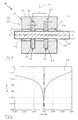
- Fig. 1 shows a shielding device 10 for a microwave oven, wherein the shielding device 10 is inserted tightly into a wall 11 of a treatment chamber 12 of the microwave oven not shown here.
- a drive which is likewise not shown here in detail, is arranged for an axis 14 of the shielding device 10, wherein the drive for Movement of a located on the axis 14 within the treatment chamber 12 and also not shown reflection rotary mirror is used.
- the shielding device 10 furthermore has an bushing device 15 with a through-bore 16 in a body 17 of the bushing device 15.
- the axis 14 is performed through the through hole 16 of the body 17 of the outer region 13 into the treatment chamber 12, wherein a gap 18 with a constant gap s between a diameter d of the axis 14 and the through hole 16 and inner surface 19 of the body 17 is formed , As a dielectric for the gap 18 here air is provided.
- 16 two reflection traps 20 and 21 are arranged within the through hole, which are each formed by a gap paragraph 22, in which a dielectric element 23 and 24 is used.
- the gap paragraph 22 in this case has an extended gap s' with a width b, which are selected so that the reflection traps 20 and 21 each have a plurality of resonant frequencies of a microwave band of the microwave device or a magnetron of the microwave device. Further, the reflection traps 20 and 21 are arranged at a center distance m relative to each other so that the center distance m corresponds to half a wavelength ⁇ of a microwave band. As a result, a particularly good shielding of the microwave band can be achieved. Also, the dielectric elements 23 and 24 are each formed of different dielectric materials in order to be able to absorb or reflect the widest possible bandwidth of microwaves.
- the dielectric elements 23 and 24 thereby come into contact with a surface 25 of the axis 14, so that the dielectric elements 23 and 24 form a bearing 26 for the axis 14.
- a bearing of the axis 14 to a drive no further storage of the axle 14 is required.
- the Fig. 2 shows a transmission curve 27 formed by a not shown here shielding band-stop filter in a frequency range of a microwave device of about 2.45 GHz.
- a filter in the frequency range of 2.4 GHz to 2.5 GHz around an ISM band of 2.45 GHz has a transmission of -40 dB.
- the filter is formed by a possible embodiment of a shielding device.
- the transmission corresponds to a damping of a maximum possible radiated power of the microwave oven by a factor of 10,000. If the relevant shielding device is subjected, for example, to 10,000 watts as the maximum power of the microwave device, only a power of one watt can pass through the filter or the band-stop filter formed by the shielding device.
Landscapes
- Physics & Mathematics (AREA)
- Electromagnetism (AREA)
- Constitution Of High-Frequency Heating (AREA)
Priority Applications (1)
| Application Number | Priority Date | Filing Date | Title |
|---|---|---|---|
| EP14158172.8A EP2916618B1 (fr) | 2014-03-06 | 2014-03-06 | Dispositif de blindage pour appareil à micro-ondes |
Applications Claiming Priority (1)
| Application Number | Priority Date | Filing Date | Title |
|---|---|---|---|
| EP14158172.8A EP2916618B1 (fr) | 2014-03-06 | 2014-03-06 | Dispositif de blindage pour appareil à micro-ondes |
Publications (3)
| Publication Number | Publication Date |
|---|---|
| EP2916618A1 true EP2916618A1 (fr) | 2015-09-09 |
| EP2916618A8 EP2916618A8 (fr) | 2015-10-21 |
| EP2916618B1 EP2916618B1 (fr) | 2018-11-14 |
Family
ID=50239428
Family Applications (1)
| Application Number | Title | Priority Date | Filing Date |
|---|---|---|---|
| EP14158172.8A Active EP2916618B1 (fr) | 2014-03-06 | 2014-03-06 | Dispositif de blindage pour appareil à micro-ondes |
Country Status (1)
| Country | Link |
|---|---|
| EP (1) | EP2916618B1 (fr) |
Cited By (1)
| Publication number | Priority date | Publication date | Assignee | Title |
|---|---|---|---|---|
| WO2020188075A1 (fr) * | 2019-03-20 | 2020-09-24 | Karlsruher Institut für Technologie | Procédé de fabrication additive d'un moule à l'aide d'un faisceau de micro-ondes, dispositif d'impression à micro-ondes et dispositif d'impression additive destiné à l'impression 3d d'un filament comprenant une matière composite fibreuse |
Citations (6)
| Publication number | Priority date | Publication date | Assignee | Title |
|---|---|---|---|---|
| DE3736556A1 (de) * | 1986-10-28 | 1988-05-11 | Gold Star Co | Schutzvorrichtung fuer die drehtellerwelle eines mikrowellenherds |
| DE3739032A1 (de) * | 1987-11-17 | 1989-05-24 | Bosch Siemens Hausgeraete | Lagerung einer drehantenne in einem mikrowellengeraet |
| JPH01204387A (ja) * | 1988-02-09 | 1989-08-16 | Hitachi Heating Appliance Co Ltd | 高周波加熱装置 |
| US6127665A (en) * | 1997-08-08 | 2000-10-03 | Sharp Kabushiki Kaisha | High frequency heating apparatus having a mechanism for preventing leakage of radio waves |
| EP1639865B1 (fr) | 2003-07-01 | 2007-02-14 | Forschungszentrum Karlsruhe GmbH | Resonateur micro-ondes, chaine de processus constituee selon le principe modulaire a partir d'un resonateur micro-ondes, procede de fonctionnement et objets/pieces traites thermiquement par micro-onde selon ce procede |
| WO2011080204A1 (fr) * | 2009-12-30 | 2011-07-07 | Arcelik Anonim Sirketi | Four |
-
2014
- 2014-03-06 EP EP14158172.8A patent/EP2916618B1/fr active Active
Patent Citations (6)
| Publication number | Priority date | Publication date | Assignee | Title |
|---|---|---|---|---|
| DE3736556A1 (de) * | 1986-10-28 | 1988-05-11 | Gold Star Co | Schutzvorrichtung fuer die drehtellerwelle eines mikrowellenherds |
| DE3739032A1 (de) * | 1987-11-17 | 1989-05-24 | Bosch Siemens Hausgeraete | Lagerung einer drehantenne in einem mikrowellengeraet |
| JPH01204387A (ja) * | 1988-02-09 | 1989-08-16 | Hitachi Heating Appliance Co Ltd | 高周波加熱装置 |
| US6127665A (en) * | 1997-08-08 | 2000-10-03 | Sharp Kabushiki Kaisha | High frequency heating apparatus having a mechanism for preventing leakage of radio waves |
| EP1639865B1 (fr) | 2003-07-01 | 2007-02-14 | Forschungszentrum Karlsruhe GmbH | Resonateur micro-ondes, chaine de processus constituee selon le principe modulaire a partir d'un resonateur micro-ondes, procede de fonctionnement et objets/pieces traites thermiquement par micro-onde selon ce procede |
| WO2011080204A1 (fr) * | 2009-12-30 | 2011-07-07 | Arcelik Anonim Sirketi | Four |
Cited By (2)
| Publication number | Priority date | Publication date | Assignee | Title |
|---|---|---|---|---|
| WO2020188075A1 (fr) * | 2019-03-20 | 2020-09-24 | Karlsruher Institut für Technologie | Procédé de fabrication additive d'un moule à l'aide d'un faisceau de micro-ondes, dispositif d'impression à micro-ondes et dispositif d'impression additive destiné à l'impression 3d d'un filament comprenant une matière composite fibreuse |
| US12109755B2 (en) | 2019-03-20 | 2024-10-08 | Karlsruher Institut für Technologie | Additive manufacturing process of a mould using microwave radiation, microwave printing device and additive printing device for 3D printing of a filament comprising a fibre composite material |
Also Published As
| Publication number | Publication date |
|---|---|
| EP2916618B1 (fr) | 2018-11-14 |
| EP2916618A8 (fr) | 2015-10-21 |
Similar Documents
| Publication | Publication Date | Title |
|---|---|---|
| DE69426463T2 (de) | Mikrowellenplasmareaktor | |
| DE602004006706T2 (de) | Vorrichtung und Verfahren zum Herstellen einer Vorform durch chemische Abscheidung aus der Dampfphase mittels Plasma | |
| DE3117709A1 (de) | Mikrowellenzufuehrungseinrichtung fuer mikrowellenoefen | |
| WO2019243922A1 (fr) | Ensemble appareil de cuisson | |
| EP2916618B1 (fr) | Dispositif de blindage pour appareil à micro-ondes | |
| WO2019057734A1 (fr) | Dispositif pour traiter un produit au moyen de micro-ondes | |
| CH639807A5 (de) | Kombinierter herd fuer mikrowellen- und widerstandsheizung. | |
| DE3029648A1 (de) | Mikrowellenheizvorrichtung | |
| EP2749151B1 (fr) | Résonateur haute fréquence et accélérateur de particules comportant un tel résonateur haute fréquence | |
| EP3560280A1 (fr) | Dispositif pour appareil de cuisson | |
| DE102011082580A1 (de) | HF-Resonator und Teilchenbeschleuniger mit HF-Resonator | |
| DE2236234C3 (de) | Dielektrisches Fenster für Mikrowellenenergie | |
| EP2187700A1 (fr) | Appareil de cuisson et procédé d'alimentation en micro-ondes dans la chambre interne d'un appareil de cuisson | |
| EP3643141A1 (fr) | Appareil de cuisson à micro-ondes à antenne planaire | |
| WO2015193065A1 (fr) | Tube commutateur à vide et procédé de fabrication d'un tube commutateur à vide | |
| DE102008001637B4 (de) | Mikrowellenofen zur thermischen Behandlung von Gütern | |
| DE7833977U1 (de) | Herd oder ofen fuer verbundbetrieb mit mikrowellenenergie und widerstandsheizung | |
| DE6932677U (de) | Hochfrequenzfilter zur stoerstrahlungsunterdrueckung | |
| WO2019243919A1 (fr) | Ensemble four à induction | |
| DE2632404B2 (de) | Hochfrequenz-Elektronenröhre mit einer Einrichtung zur Dämpfung von Hohlraum-Störwellen | |
| DE2832914A1 (de) | Mikrowellenbrat- oder backrohr | |
| DE1942115C3 (de) | Hochfrequenzfilter zur Störstrahlungsunterdrückung | |
| DE3030627A1 (de) | Anordnung zum ankoppeln einer rotierenden antenne an eine hochfrequenzleitung, insbesondere fuer hochfrequenzheizgeraete | |
| EP3987888B1 (fr) | Appareil ménager à micro-ondes équipé d'une antenne rotative | |
| DE19700140A1 (de) | Brennofen für die Hochtemperaturbehandlung von Materialien mit niedrigem dielektrischem Verlustfaktor |
Legal Events
| Date | Code | Title | Description |
|---|---|---|---|
| PUAI | Public reference made under article 153(3) epc to a published international application that has entered the european phase |
Free format text: ORIGINAL CODE: 0009012 |
|
| AK | Designated contracting states |
Kind code of ref document: A1 Designated state(s): AL AT BE BG CH CY CZ DE DK EE ES FI FR GB GR HR HU IE IS IT LI LT LU LV MC MK MT NL NO PL PT RO RS SE SI SK SM TR |
|
| AX | Request for extension of the european patent |
Extension state: BA ME |
|
| RIN1 | Information on inventor provided before grant (corrected) |
Inventor name: BETZ, STEFAN, DIPL.-ING. Inventor name: SCHMIDT, JOCHEN, DIPL.-ING. Inventor name: LINK, GUIDO, DR. Inventor name: KAYSER, THORSTEN, DR. |
|
| RIN1 | Information on inventor provided before grant (corrected) |
Inventor name: LINK, GUIDO, DR. Inventor name: SCHMIDT, JOCHEN, DIPL.-ING. Inventor name: KAYSER, THORSTEN, DR. Inventor name: BETZ, STEFAN, DIPL.-ING. |
|
| 17P | Request for examination filed |
Effective date: 20160303 |
|
| RBV | Designated contracting states (corrected) |
Designated state(s): AL AT BE BG CH CY CZ DE DK EE ES FI FR GB GR HR HU IE IS IT LI LT LU LV MC MK MT NL NO PL PT RO RS SE SI SK SM TR |
|
| REG | Reference to a national code |
Ref country code: DE Ref legal event code: R079 Ref document number: 502014010027 Country of ref document: DE Free format text: PREVIOUS MAIN CLASS: H05B0006640000 Ipc: H05B0006760000 |
|
| GRAP | Despatch of communication of intention to grant a patent |
Free format text: ORIGINAL CODE: EPIDOSNIGR1 |
|
| STAA | Information on the status of an ep patent application or granted ep patent |
Free format text: STATUS: GRANT OF PATENT IS INTENDED |
|
| RIC1 | Information provided on ipc code assigned before grant |
Ipc: H05B 6/78 20060101ALI20180514BHEP Ipc: H05B 6/76 20060101AFI20180514BHEP |
|
| INTG | Intention to grant announced |
Effective date: 20180604 |
|
| GRAS | Grant fee paid |
Free format text: ORIGINAL CODE: EPIDOSNIGR3 |
|
| GRAA | (expected) grant |
Free format text: ORIGINAL CODE: 0009210 |
|
| STAA | Information on the status of an ep patent application or granted ep patent |
Free format text: STATUS: THE PATENT HAS BEEN GRANTED |
|
| AK | Designated contracting states |
Kind code of ref document: B1 Designated state(s): AL AT BE BG CH CY CZ DE DK EE ES FI FR GB GR HR HU IE IS IT LI LT LU LV MC MK MT NL NO PL PT RO RS SE SI SK SM TR |
|
| REG | Reference to a national code |
Ref country code: CH Ref legal event code: EP Ref country code: AT Ref legal event code: REF Ref document number: 1066376 Country of ref document: AT Kind code of ref document: T Effective date: 20181115 |
|
| REG | Reference to a national code |
Ref country code: DE Ref legal event code: R096 Ref document number: 502014010027 Country of ref document: DE |
|
| REG | Reference to a national code |
Ref country code: IE Ref legal event code: FG4D Free format text: LANGUAGE OF EP DOCUMENT: GERMAN |
|
| REG | Reference to a national code |
Ref country code: NL Ref legal event code: MP Effective date: 20181114 |
|
| REG | Reference to a national code |
Ref country code: LT Ref legal event code: MG4D |
|
| PG25 | Lapsed in a contracting state [announced via postgrant information from national office to epo] |
Ref country code: IS Free format text: LAPSE BECAUSE OF FAILURE TO SUBMIT A TRANSLATION OF THE DESCRIPTION OR TO PAY THE FEE WITHIN THE PRESCRIBED TIME-LIMIT Effective date: 20190314 Ref country code: FI Free format text: LAPSE BECAUSE OF FAILURE TO SUBMIT A TRANSLATION OF THE DESCRIPTION OR TO PAY THE FEE WITHIN THE PRESCRIBED TIME-LIMIT Effective date: 20181114 Ref country code: HR Free format text: LAPSE BECAUSE OF FAILURE TO SUBMIT A TRANSLATION OF THE DESCRIPTION OR TO PAY THE FEE WITHIN THE PRESCRIBED TIME-LIMIT Effective date: 20181114 Ref country code: LT Free format text: LAPSE BECAUSE OF FAILURE TO SUBMIT A TRANSLATION OF THE DESCRIPTION OR TO PAY THE FEE WITHIN THE PRESCRIBED TIME-LIMIT Effective date: 20181114 Ref country code: NO Free format text: LAPSE BECAUSE OF FAILURE TO SUBMIT A TRANSLATION OF THE DESCRIPTION OR TO PAY THE FEE WITHIN THE PRESCRIBED TIME-LIMIT Effective date: 20190214 Ref country code: LV Free format text: LAPSE BECAUSE OF FAILURE TO SUBMIT A TRANSLATION OF THE DESCRIPTION OR TO PAY THE FEE WITHIN THE PRESCRIBED TIME-LIMIT Effective date: 20181114 Ref country code: ES Free format text: LAPSE BECAUSE OF FAILURE TO SUBMIT A TRANSLATION OF THE DESCRIPTION OR TO PAY THE FEE WITHIN THE PRESCRIBED TIME-LIMIT Effective date: 20181114 Ref country code: BG Free format text: LAPSE BECAUSE OF FAILURE TO SUBMIT A TRANSLATION OF THE DESCRIPTION OR TO PAY THE FEE WITHIN THE PRESCRIBED TIME-LIMIT Effective date: 20190214 |
|
| PG25 | Lapsed in a contracting state [announced via postgrant information from national office to epo] |
Ref country code: AL Free format text: LAPSE BECAUSE OF FAILURE TO SUBMIT A TRANSLATION OF THE DESCRIPTION OR TO PAY THE FEE WITHIN THE PRESCRIBED TIME-LIMIT Effective date: 20181114 Ref country code: PT Free format text: LAPSE BECAUSE OF FAILURE TO SUBMIT A TRANSLATION OF THE DESCRIPTION OR TO PAY THE FEE WITHIN THE PRESCRIBED TIME-LIMIT Effective date: 20190314 Ref country code: SE Free format text: LAPSE BECAUSE OF FAILURE TO SUBMIT A TRANSLATION OF THE DESCRIPTION OR TO PAY THE FEE WITHIN THE PRESCRIBED TIME-LIMIT Effective date: 20181114 Ref country code: NL Free format text: LAPSE BECAUSE OF FAILURE TO SUBMIT A TRANSLATION OF THE DESCRIPTION OR TO PAY THE FEE WITHIN THE PRESCRIBED TIME-LIMIT Effective date: 20181114 Ref country code: GR Free format text: LAPSE BECAUSE OF FAILURE TO SUBMIT A TRANSLATION OF THE DESCRIPTION OR TO PAY THE FEE WITHIN THE PRESCRIBED TIME-LIMIT Effective date: 20190215 Ref country code: RS Free format text: LAPSE BECAUSE OF FAILURE TO SUBMIT A TRANSLATION OF THE DESCRIPTION OR TO PAY THE FEE WITHIN THE PRESCRIBED TIME-LIMIT Effective date: 20181114 |
|
| PG25 | Lapsed in a contracting state [announced via postgrant information from national office to epo] |
Ref country code: CZ Free format text: LAPSE BECAUSE OF FAILURE TO SUBMIT A TRANSLATION OF THE DESCRIPTION OR TO PAY THE FEE WITHIN THE PRESCRIBED TIME-LIMIT Effective date: 20181114 Ref country code: PL Free format text: LAPSE BECAUSE OF FAILURE TO SUBMIT A TRANSLATION OF THE DESCRIPTION OR TO PAY THE FEE WITHIN THE PRESCRIBED TIME-LIMIT Effective date: 20181114 Ref country code: IT Free format text: LAPSE BECAUSE OF FAILURE TO SUBMIT A TRANSLATION OF THE DESCRIPTION OR TO PAY THE FEE WITHIN THE PRESCRIBED TIME-LIMIT Effective date: 20181114 Ref country code: DK Free format text: LAPSE BECAUSE OF FAILURE TO SUBMIT A TRANSLATION OF THE DESCRIPTION OR TO PAY THE FEE WITHIN THE PRESCRIBED TIME-LIMIT Effective date: 20181114 |
|
| REG | Reference to a national code |
Ref country code: DE Ref legal event code: R097 Ref document number: 502014010027 Country of ref document: DE |
|
| PG25 | Lapsed in a contracting state [announced via postgrant information from national office to epo] |
Ref country code: EE Free format text: LAPSE BECAUSE OF FAILURE TO SUBMIT A TRANSLATION OF THE DESCRIPTION OR TO PAY THE FEE WITHIN THE PRESCRIBED TIME-LIMIT Effective date: 20181114 Ref country code: SM Free format text: LAPSE BECAUSE OF FAILURE TO SUBMIT A TRANSLATION OF THE DESCRIPTION OR TO PAY THE FEE WITHIN THE PRESCRIBED TIME-LIMIT Effective date: 20181114 Ref country code: RO Free format text: LAPSE BECAUSE OF FAILURE TO SUBMIT A TRANSLATION OF THE DESCRIPTION OR TO PAY THE FEE WITHIN THE PRESCRIBED TIME-LIMIT Effective date: 20181114 Ref country code: SK Free format text: LAPSE BECAUSE OF FAILURE TO SUBMIT A TRANSLATION OF THE DESCRIPTION OR TO PAY THE FEE WITHIN THE PRESCRIBED TIME-LIMIT Effective date: 20181114 |
|
| PLBE | No opposition filed within time limit |
Free format text: ORIGINAL CODE: 0009261 |
|
| STAA | Information on the status of an ep patent application or granted ep patent |
Free format text: STATUS: NO OPPOSITION FILED WITHIN TIME LIMIT |
|
| 26N | No opposition filed |
Effective date: 20190815 |
|
| PG25 | Lapsed in a contracting state [announced via postgrant information from national office to epo] |
Ref country code: MC Free format text: LAPSE BECAUSE OF FAILURE TO SUBMIT A TRANSLATION OF THE DESCRIPTION OR TO PAY THE FEE WITHIN THE PRESCRIBED TIME-LIMIT Effective date: 20181114 Ref country code: SI Free format text: LAPSE BECAUSE OF FAILURE TO SUBMIT A TRANSLATION OF THE DESCRIPTION OR TO PAY THE FEE WITHIN THE PRESCRIBED TIME-LIMIT Effective date: 20181114 |
|
| REG | Reference to a national code |
Ref country code: CH Ref legal event code: PL |
|
| PG25 | Lapsed in a contracting state [announced via postgrant information from national office to epo] |
Ref country code: LU Free format text: LAPSE BECAUSE OF NON-PAYMENT OF DUE FEES Effective date: 20190306 |
|
| REG | Reference to a national code |
Ref country code: BE Ref legal event code: MM Effective date: 20190331 |
|
| PG25 | Lapsed in a contracting state [announced via postgrant information from national office to epo] |
Ref country code: IE Free format text: LAPSE BECAUSE OF NON-PAYMENT OF DUE FEES Effective date: 20190306 Ref country code: LI Free format text: LAPSE BECAUSE OF NON-PAYMENT OF DUE FEES Effective date: 20190331 Ref country code: CH Free format text: LAPSE BECAUSE OF NON-PAYMENT OF DUE FEES Effective date: 20190331 |
|
| PG25 | Lapsed in a contracting state [announced via postgrant information from national office to epo] |
Ref country code: BE Free format text: LAPSE BECAUSE OF NON-PAYMENT OF DUE FEES Effective date: 20190331 |
|
| PG25 | Lapsed in a contracting state [announced via postgrant information from national office to epo] |
Ref country code: TR Free format text: LAPSE BECAUSE OF FAILURE TO SUBMIT A TRANSLATION OF THE DESCRIPTION OR TO PAY THE FEE WITHIN THE PRESCRIBED TIME-LIMIT Effective date: 20181114 |
|
| PGFP | Annual fee paid to national office [announced via postgrant information from national office to epo] |
Ref country code: GB Payment date: 20200327 Year of fee payment: 7 |
|
| PG25 | Lapsed in a contracting state [announced via postgrant information from national office to epo] |
Ref country code: MT Free format text: LAPSE BECAUSE OF FAILURE TO SUBMIT A TRANSLATION OF THE DESCRIPTION OR TO PAY THE FEE WITHIN THE PRESCRIBED TIME-LIMIT Effective date: 20181114 |
|
| PGFP | Annual fee paid to national office [announced via postgrant information from national office to epo] |
Ref country code: FR Payment date: 20200326 Year of fee payment: 7 |
|
| REG | Reference to a national code |
Ref country code: AT Ref legal event code: MM01 Ref document number: 1066376 Country of ref document: AT Kind code of ref document: T Effective date: 20190306 |
|
| PG25 | Lapsed in a contracting state [announced via postgrant information from national office to epo] |
Ref country code: AT Free format text: LAPSE BECAUSE OF NON-PAYMENT OF DUE FEES Effective date: 20190306 |
|
| PG25 | Lapsed in a contracting state [announced via postgrant information from national office to epo] |
Ref country code: CY Free format text: LAPSE BECAUSE OF FAILURE TO SUBMIT A TRANSLATION OF THE DESCRIPTION OR TO PAY THE FEE WITHIN THE PRESCRIBED TIME-LIMIT Effective date: 20181114 |
|
| PG25 | Lapsed in a contracting state [announced via postgrant information from national office to epo] |
Ref country code: HU Free format text: LAPSE BECAUSE OF FAILURE TO SUBMIT A TRANSLATION OF THE DESCRIPTION OR TO PAY THE FEE WITHIN THE PRESCRIBED TIME-LIMIT; INVALID AB INITIO Effective date: 20140306 |
|
| GBPC | Gb: european patent ceased through non-payment of renewal fee |
Effective date: 20210306 |
|
| PG25 | Lapsed in a contracting state [announced via postgrant information from national office to epo] |
Ref country code: GB Free format text: LAPSE BECAUSE OF NON-PAYMENT OF DUE FEES Effective date: 20210306 Ref country code: FR Free format text: LAPSE BECAUSE OF NON-PAYMENT OF DUE FEES Effective date: 20210331 |
|
| PG25 | Lapsed in a contracting state [announced via postgrant information from national office to epo] |
Ref country code: MK Free format text: LAPSE BECAUSE OF FAILURE TO SUBMIT A TRANSLATION OF THE DESCRIPTION OR TO PAY THE FEE WITHIN THE PRESCRIBED TIME-LIMIT Effective date: 20181114 |
|
| P01 | Opt-out of the competence of the unified patent court (upc) registered |
Effective date: 20230524 |
|
| PGFP | Annual fee paid to national office [announced via postgrant information from national office to epo] |
Ref country code: DE Payment date: 20260320 Year of fee payment: 13 |