EP2918708A2 - Procédés de dopage réglable de cristaux massifs de nitrure d'aluminium - Google Patents
Procédés de dopage réglable de cristaux massifs de nitrure d'aluminium Download PDFInfo
- Publication number
- EP2918708A2 EP2918708A2 EP15154002.8A EP15154002A EP2918708A2 EP 2918708 A2 EP2918708 A2 EP 2918708A2 EP 15154002 A EP15154002 A EP 15154002A EP 2918708 A2 EP2918708 A2 EP 2918708A2
- Authority
- EP
- European Patent Office
- Prior art keywords
- aln
- approximately
- crystal
- annealing
- nitrogen
- Prior art date
- Legal status (The legal status is an assumption and is not a legal conclusion. Google has not performed a legal analysis and makes no representation as to the accuracy of the status listed.)
- Granted
Links
Images



Classifications
-
- C—CHEMISTRY; METALLURGY
- C04—CEMENTS; CONCRETE; ARTIFICIAL STONE; CERAMICS; REFRACTORIES
- C04B—LIME, MAGNESIA; SLAG; CEMENTS; COMPOSITIONS THEREOF, e.g. MORTARS, CONCRETE OR LIKE BUILDING MATERIALS; ARTIFICIAL STONE; CERAMICS; REFRACTORIES; TREATMENT OF NATURAL STONE
- C04B35/00—Shaped ceramic products characterised by their composition; Ceramics compositions; Processing powders of inorganic compounds preparatory to the manufacturing of ceramic products
- C04B35/515—Shaped ceramic products characterised by their composition; Ceramics compositions; Processing powders of inorganic compounds preparatory to the manufacturing of ceramic products based on non-oxide ceramics
- C04B35/58—Shaped ceramic products characterised by their composition; Ceramics compositions; Processing powders of inorganic compounds preparatory to the manufacturing of ceramic products based on non-oxide ceramics based on borides, nitrides, i.e. nitrides, oxynitrides, carbonitrides or oxycarbonitrides or silicides
- C04B35/581—Shaped ceramic products characterised by their composition; Ceramics compositions; Processing powders of inorganic compounds preparatory to the manufacturing of ceramic products based on non-oxide ceramics based on borides, nitrides, i.e. nitrides, oxynitrides, carbonitrides or oxycarbonitrides or silicides based on aluminium nitride
-
- C—CHEMISTRY; METALLURGY
- C01—INORGANIC CHEMISTRY
- C01B—NON-METALLIC ELEMENTS; COMPOUNDS THEREOF; METALLOIDS OR COMPOUNDS THEREOF NOT COVERED BY SUBCLASS C01C
- C01B21/00—Nitrogen; Compounds thereof
- C01B21/06—Binary compounds of nitrogen with metals, with silicon, or with boron, or with carbon, i.e. nitrides; Compounds of nitrogen with more than one metal, silicon or boron
- C01B21/072—Binary compounds of nitrogen with metals, with silicon, or with boron, or with carbon, i.e. nitrides; Compounds of nitrogen with more than one metal, silicon or boron with aluminium
- C01B21/0722—Preparation by direct nitridation of aluminium
-
- C—CHEMISTRY; METALLURGY
- C04—CEMENTS; CONCRETE; ARTIFICIAL STONE; CERAMICS; REFRACTORIES
- C04B—LIME, MAGNESIA; SLAG; CEMENTS; COMPOSITIONS THEREOF, e.g. MORTARS, CONCRETE OR LIKE BUILDING MATERIALS; ARTIFICIAL STONE; CERAMICS; REFRACTORIES; TREATMENT OF NATURAL STONE
- C04B35/00—Shaped ceramic products characterised by their composition; Ceramics compositions; Processing powders of inorganic compounds preparatory to the manufacturing of ceramic products
- C04B35/622—Forming processes; Processing powders of inorganic compounds preparatory to the manufacturing of ceramic products
- C04B35/64—Burning or sintering processes
- C04B35/65—Reaction sintering of free metal- or free silicon-containing compositions
-
- C—CHEMISTRY; METALLURGY
- C30—CRYSTAL GROWTH
- C30B—SINGLE-CRYSTAL GROWTH; UNIDIRECTIONAL SOLIDIFICATION OF EUTECTIC MATERIAL OR UNIDIRECTIONAL DEMIXING OF EUTECTOID MATERIAL; REFINING BY ZONE-MELTING OF MATERIAL; PRODUCTION OF A HOMOGENEOUS POLYCRYSTALLINE MATERIAL WITH DEFINED STRUCTURE; SINGLE CRYSTALS OR HOMOGENEOUS POLYCRYSTALLINE MATERIAL WITH DEFINED STRUCTURE; AFTER-TREATMENT OF SINGLE CRYSTALS OR A HOMOGENEOUS POLYCRYSTALLINE MATERIAL WITH DEFINED STRUCTURE; APPARATUS THEREFOR
- C30B23/00—Single-crystal growth by condensing evaporated or sublimed materials
-
- C—CHEMISTRY; METALLURGY
- C30—CRYSTAL GROWTH
- C30B—SINGLE-CRYSTAL GROWTH; UNIDIRECTIONAL SOLIDIFICATION OF EUTECTIC MATERIAL OR UNIDIRECTIONAL DEMIXING OF EUTECTOID MATERIAL; REFINING BY ZONE-MELTING OF MATERIAL; PRODUCTION OF A HOMOGENEOUS POLYCRYSTALLINE MATERIAL WITH DEFINED STRUCTURE; SINGLE CRYSTALS OR HOMOGENEOUS POLYCRYSTALLINE MATERIAL WITH DEFINED STRUCTURE; AFTER-TREATMENT OF SINGLE CRYSTALS OR A HOMOGENEOUS POLYCRYSTALLINE MATERIAL WITH DEFINED STRUCTURE; APPARATUS THEREFOR
- C30B29/00—Single crystals or homogeneous polycrystalline material with defined structure characterised by the material or by their shape
- C30B29/10—Inorganic compounds or compositions
- C30B29/40—AIIIBV compounds wherein A is B, Al, Ga, In or Tl and B is N, P, As, Sb or Bi
- C30B29/403—AIII-nitrides
-
- C—CHEMISTRY; METALLURGY
- C30—CRYSTAL GROWTH
- C30B—SINGLE-CRYSTAL GROWTH; UNIDIRECTIONAL SOLIDIFICATION OF EUTECTIC MATERIAL OR UNIDIRECTIONAL DEMIXING OF EUTECTOID MATERIAL; REFINING BY ZONE-MELTING OF MATERIAL; PRODUCTION OF A HOMOGENEOUS POLYCRYSTALLINE MATERIAL WITH DEFINED STRUCTURE; SINGLE CRYSTALS OR HOMOGENEOUS POLYCRYSTALLINE MATERIAL WITH DEFINED STRUCTURE; AFTER-TREATMENT OF SINGLE CRYSTALS OR A HOMOGENEOUS POLYCRYSTALLINE MATERIAL WITH DEFINED STRUCTURE; APPARATUS THEREFOR
- C30B33/00—After-treatment of single crystals or homogeneous polycrystalline material with defined structure
- C30B33/02—Heat treatment
-
- C—CHEMISTRY; METALLURGY
- C04—CEMENTS; CONCRETE; ARTIFICIAL STONE; CERAMICS; REFRACTORIES
- C04B—LIME, MAGNESIA; SLAG; CEMENTS; COMPOSITIONS THEREOF, e.g. MORTARS, CONCRETE OR LIKE BUILDING MATERIALS; ARTIFICIAL STONE; CERAMICS; REFRACTORIES; TREATMENT OF NATURAL STONE
- C04B2235/00—Aspects relating to ceramic starting mixtures or sintered ceramic products
- C04B2235/02—Composition of constituents of the starting material or of secondary phases of the final product
- C04B2235/30—Constituents and secondary phases not being of a fibrous nature
- C04B2235/38—Non-oxide ceramic constituents or additives
- C04B2235/3852—Nitrides, e.g. oxynitrides, carbonitrides, oxycarbonitrides, lithium nitride, magnesium nitride
-
- C—CHEMISTRY; METALLURGY
- C04—CEMENTS; CONCRETE; ARTIFICIAL STONE; CERAMICS; REFRACTORIES
- C04B—LIME, MAGNESIA; SLAG; CEMENTS; COMPOSITIONS THEREOF, e.g. MORTARS, CONCRETE OR LIKE BUILDING MATERIALS; ARTIFICIAL STONE; CERAMICS; REFRACTORIES; TREATMENT OF NATURAL STONE
- C04B2235/00—Aspects relating to ceramic starting mixtures or sintered ceramic products
- C04B2235/02—Composition of constituents of the starting material or of secondary phases of the final product
- C04B2235/30—Constituents and secondary phases not being of a fibrous nature
- C04B2235/38—Non-oxide ceramic constituents or additives
- C04B2235/3852—Nitrides, e.g. oxynitrides, carbonitrides, oxycarbonitrides, lithium nitride, magnesium nitride
- C04B2235/3856—Carbonitrides, e.g. titanium carbonitride, zirconium carbonitride
-
- C—CHEMISTRY; METALLURGY
- C04—CEMENTS; CONCRETE; ARTIFICIAL STONE; CERAMICS; REFRACTORIES
- C04B—LIME, MAGNESIA; SLAG; CEMENTS; COMPOSITIONS THEREOF, e.g. MORTARS, CONCRETE OR LIKE BUILDING MATERIALS; ARTIFICIAL STONE; CERAMICS; REFRACTORIES; TREATMENT OF NATURAL STONE
- C04B2235/00—Aspects relating to ceramic starting mixtures or sintered ceramic products
- C04B2235/02—Composition of constituents of the starting material or of secondary phases of the final product
- C04B2235/30—Constituents and secondary phases not being of a fibrous nature
- C04B2235/38—Non-oxide ceramic constituents or additives
- C04B2235/3852—Nitrides, e.g. oxynitrides, carbonitrides, oxycarbonitrides, lithium nitride, magnesium nitride
- C04B2235/3873—Silicon nitrides, e.g. silicon carbonitride, silicon oxynitride
-
- C—CHEMISTRY; METALLURGY
- C04—CEMENTS; CONCRETE; ARTIFICIAL STONE; CERAMICS; REFRACTORIES
- C04B—LIME, MAGNESIA; SLAG; CEMENTS; COMPOSITIONS THEREOF, e.g. MORTARS, CONCRETE OR LIKE BUILDING MATERIALS; ARTIFICIAL STONE; CERAMICS; REFRACTORIES; TREATMENT OF NATURAL STONE
- C04B2235/00—Aspects relating to ceramic starting mixtures or sintered ceramic products
- C04B2235/02—Composition of constituents of the starting material or of secondary phases of the final product
- C04B2235/30—Constituents and secondary phases not being of a fibrous nature
- C04B2235/40—Metallic constituents or additives not added as binding phase
- C04B2235/402—Aluminium
-
- C—CHEMISTRY; METALLURGY
- C04—CEMENTS; CONCRETE; ARTIFICIAL STONE; CERAMICS; REFRACTORIES
- C04B—LIME, MAGNESIA; SLAG; CEMENTS; COMPOSITIONS THEREOF, e.g. MORTARS, CONCRETE OR LIKE BUILDING MATERIALS; ARTIFICIAL STONE; CERAMICS; REFRACTORIES; TREATMENT OF NATURAL STONE
- C04B2235/00—Aspects relating to ceramic starting mixtures or sintered ceramic products
- C04B2235/02—Composition of constituents of the starting material or of secondary phases of the final product
- C04B2235/30—Constituents and secondary phases not being of a fibrous nature
- C04B2235/42—Non metallic elements added as constituents or additives, e.g. sulfur, phosphor, selenium or tellurium
- C04B2235/428—Silicon
-
- C—CHEMISTRY; METALLURGY
- C04—CEMENTS; CONCRETE; ARTIFICIAL STONE; CERAMICS; REFRACTORIES
- C04B—LIME, MAGNESIA; SLAG; CEMENTS; COMPOSITIONS THEREOF, e.g. MORTARS, CONCRETE OR LIKE BUILDING MATERIALS; ARTIFICIAL STONE; CERAMICS; REFRACTORIES; TREATMENT OF NATURAL STONE
- C04B2235/00—Aspects relating to ceramic starting mixtures or sintered ceramic products
- C04B2235/02—Composition of constituents of the starting material or of secondary phases of the final product
- C04B2235/30—Constituents and secondary phases not being of a fibrous nature
- C04B2235/46—Gases other than oxygen used as reactant, e.g. nitrogen used to make a nitride phase
-
- C—CHEMISTRY; METALLURGY
- C04—CEMENTS; CONCRETE; ARTIFICIAL STONE; CERAMICS; REFRACTORIES
- C04B—LIME, MAGNESIA; SLAG; CEMENTS; COMPOSITIONS THEREOF, e.g. MORTARS, CONCRETE OR LIKE BUILDING MATERIALS; ARTIFICIAL STONE; CERAMICS; REFRACTORIES; TREATMENT OF NATURAL STONE
- C04B2235/00—Aspects relating to ceramic starting mixtures or sintered ceramic products
- C04B2235/65—Aspects relating to heat treatments of ceramic bodies such as green ceramics or pre-sintered ceramics, e.g. burning, sintering or melting processes
- C04B2235/656—Aspects relating to heat treatments of ceramic bodies such as green ceramics or pre-sintered ceramics, e.g. burning, sintering or melting processes characterised by specific heating conditions during heat treatment
-
- C—CHEMISTRY; METALLURGY
- C04—CEMENTS; CONCRETE; ARTIFICIAL STONE; CERAMICS; REFRACTORIES
- C04B—LIME, MAGNESIA; SLAG; CEMENTS; COMPOSITIONS THEREOF, e.g. MORTARS, CONCRETE OR LIKE BUILDING MATERIALS; ARTIFICIAL STONE; CERAMICS; REFRACTORIES; TREATMENT OF NATURAL STONE
- C04B2235/00—Aspects relating to ceramic starting mixtures or sintered ceramic products
- C04B2235/70—Aspects relating to sintered or melt-casted ceramic products
- C04B2235/72—Products characterised by the absence or the low content of specific components, e.g. alkali metal free alumina ceramics
-
- C—CHEMISTRY; METALLURGY
- C04—CEMENTS; CONCRETE; ARTIFICIAL STONE; CERAMICS; REFRACTORIES
- C04B—LIME, MAGNESIA; SLAG; CEMENTS; COMPOSITIONS THEREOF, e.g. MORTARS, CONCRETE OR LIKE BUILDING MATERIALS; ARTIFICIAL STONE; CERAMICS; REFRACTORIES; TREATMENT OF NATURAL STONE
- C04B2235/00—Aspects relating to ceramic starting mixtures or sintered ceramic products
- C04B2235/70—Aspects relating to sintered or melt-casted ceramic products
- C04B2235/72—Products characterised by the absence or the low content of specific components, e.g. alkali metal free alumina ceramics
- C04B2235/723—Oxygen content
-
- C—CHEMISTRY; METALLURGY
- C04—CEMENTS; CONCRETE; ARTIFICIAL STONE; CERAMICS; REFRACTORIES
- C04B—LIME, MAGNESIA; SLAG; CEMENTS; COMPOSITIONS THEREOF, e.g. MORTARS, CONCRETE OR LIKE BUILDING MATERIALS; ARTIFICIAL STONE; CERAMICS; REFRACTORIES; TREATMENT OF NATURAL STONE
- C04B2235/00—Aspects relating to ceramic starting mixtures or sintered ceramic products
- C04B2235/70—Aspects relating to sintered or melt-casted ceramic products
- C04B2235/74—Physical characteristics
- C04B2235/79—Non-stoichiometric products, e.g. perovskites (ABO3) with an A/B-ratio other than 1
Definitions
- Semiconductor materials exhibit controllable optical and electrical properties, such as conductivity, over a wide range. Such control is enabled by use of dopants, which are impurities introduced into the crystalline lattice of the semiconductor material to serve as sources of electrons (negative charges) or holes (positive charges). Controllable doping enables the fabrication of a wide range of semiconductor devices, e.g., light-emitting diodes (LEDs), lasers, and transistors.
- LEDs light-emitting diodes
- Nitride-based semiconductors such as gallium nitride (GaN) and aluminum nitride (AlN) are of great interest technologically, in part because of their wide bandgaps. Controllable and repeatable doping of these materials enables the fabrication of light-emitting devices, such as LEDs and lasers, that emit light at short wavelengths, i.e., at blue, violet, and even ultraviolet wavelengths. Moreover, n- and p-type nitrides can be utilized in the fabrication of transistors suited for high power and/or high temperature applications. In an n-type semiconductor, the concentration of electrons is much higher then the concentration of holes; accordingly, electrons are majority carriers and dominate conductivity. In a p-type semiconductor, by contrast, holes dominate conductivity.
- AlN has a relatively large bandgap of 6.1 electron volts (eV) at room temperature, and few dopants for AlN have shallow enough energy levels in the bandgap to facilitate high electrical conductivity with only moderate impurity (i.e., dopant) concentrations.
- impurity concentrations often need to be relatively high in order to achieve technologically useful conductivity levels.
- achieving high impurity concentration levels in AlN can be difficult.
- AlN is typically grown at very high temperatures, making it difficult to incorporate high levels of desired dopants in a controlled way while avoiding the introduction of unwanted impurities and other point defects. These will introduce deep levels in the bandgap that counteract the desired effect of the dopant.
- a donor or acceptor level is created within the perfect, stoichiometric AlN or Al x Ga 1-x N (where 0 ⁇ x ⁇ 1, herein sometimes referred to as AlGaN) lattice by introducing a substitutional impurity that has greater or fewer electrons than aluminum (Al) or nitrogen (N).
- Charge-compensating defects such as vacancies on the Al cation site (designated as V Al ) or the N anion site (designated as V N ) or impurities with deep levels which will trap the free charge created by the doping impurity, are desirably avoided but, more generally, are either reduced in density or less active.
- dopants are preferably selected from the upper part of the periodic table.
- Choices for the Al site include beryllium (Be), magnesium (Mg), zinc (Zn), carbon (C), and silicon (Si) while C, Si, and oxygen (O) are possible choices for the N site.
- Dopants with two fewer electrons than Al, such as lithium (Li), may also be used to make p-type AlN and AlGaN if they can be introduced on the Al site.
- the invention features a method of forming polycrystalline AlN.
- an Al-containing pellet is provided in a crucible and the pellet is reacted at a reaction temperature and a reaction pressure with nitrogen gas to form a polycrystalline AlN ceramic that is approximately stoichiometric.
- the pellet may consist essentially of Al, and the reaction temperature may be within the range of approximately 1900 °C to approximately 2200 °C.
- the pellet may include a first concentration, which may be less than approximately 12% by weight, of a dopant species, which may be Si.
- the polycrystalline AlN ceramic includes a second concentration of the dopant species. The second concentration may be less than approximately 12% by weight.
- the reaction temperature may be within the range of approximately 1600 °C to approximately 2200 °C, and the reaction pressure may be within the range of approximately 1 bar to approximately 60 bars.
- Embodiments of the invention may include one or more of the following features.
- An oxygen concentration of the polycrystalline AlN ceramic may be less than approximately 400 parts per million (ppm), or less than 100 ppm.
- Substantially all of the pellet may be reacted to form the polycrystalline AlN ceramic.
- At least one additional Al-containing pellet may be provided within the crucible and reacted at the reaction temperature and the reaction pressure with nitrogen gas in order to increase the volume of the polycrystalline AlN ceramic.
- the polycrystalline AlN ceramic is provided at the first end of and within a crystal growth enclosure and sublimed at a formation temperature, forming an AlN single crystal at the second end of the crystal growth enclosure.
- the formation temperature may be within the range of approximately 2000°C to approximately 2750 °C.
- the oxygen concentration of the AlN single crystal may be less than approximately 400 ppm, less than approximately 100 ppm, or less than approximately 4.5 ⁇ 10 19 /cm 3 .
- the thermal conductivity of the AlN single crystal may be greater than approximately 250 Watts per meter-Kelvin (W/m ⁇ K).
- the polycrystalline AlN ceramic may include a dopant species, which may be present within the AlN single crystal at a first concentration.
- the dopant species may be Si, and the first concentration may be greater than approximately 10 16 /cm 3 .
- the AlN single crystal may have a conductivity greater than approximately 10 -4 ⁇ -1 cm -1 at room temperature. At least a portion of the crucible may be proximate and in contact with the polycrystalline AlN ceramic during formation of the AlN single crystal.
- the invention features a method of forming a doped AlN wafer.
- a single-crystal wafer including AlN and a dopant species is provided and the wafer is annealed to electrically activate the dopant species.
- the dopant species may include Si.
- Annealing may decrease the concentration of aluminum vacancies, or increase the concentration of nitrogen vacancies, in the single-crystal wafer.
- the step of annealing is performed at an annealing temperature and an annealing nitrogen pressure, and the annealing nitrogen pressure is greater than approximately a nitrogen pressure required to form AlN from aluminum at the annealing temperature.
- the annealing nitrogen pressure may be less than approximately twice the nitrogen pressure required to form AlN from aluminum at the annealing temperature, or may be within the range of approximately 0.1 millibar (mbar) to approximately 5 bars.
- the annealing temperature may be greater than approximately 1900 °C.
- the single-crystal wafer may have a conductivity at room temperature greater than approximately 10 -4 ⁇ -1 cm -1 , or greater than approximately 10 -2 ⁇ -1 cm -1 .
- the invention features a method of forming an AlN wafer.
- a single-crystal wafer including undoped AlN and having a first conductivity is provided, and the single-crystal wafer is annealed in an ambient at an annealing temperature and an annealing pressure, where after annealing the single-crystal wafer has a second conductivity greater than the first conductivity.
- the annealing temperature may be within a range of approximately 1700 °C to approximately 2200 °C
- the annealing pressure may be within a range of approximately 2 bars to approximately 30 bars.
- the ambient may consist essentially of nitrogen and at least one inert gas, which may be argon.
- the pressure of nitrogen in the ambient may be greater than a nitrogen pressure required to form AlN from aluminum at the first temperature.
- the second conductivity may be greater than approximately 10 -2 ⁇ -1 cm -1 at room temperature.
- the invention features an AlN single crystal having a thickness greater than approximately 100 micrometers ( ⁇ m), a cross-sectional area greater than approximately 1 cm 2 , and a conductivity greater than approximately 10 -4 ⁇ -1 cm -1 at room temperature.
- the AlN single crystal may include a substitutional dopant species, and may exhibit n-type conductivity.
- the substitutional dopant species may include a group IV element, which may be Si.
- the AlN single crystal may consist essentially of AlN and nitrogen vacancies.
- the thickness may be greater than approximately 200 ⁇ m, or even greater than approximately 2 millimeters (mm).
- the conductivity may be greater than approximately 10 -2 ⁇ -1 cm -1 at room temperature, and a thermal conductivity of the AlN single crystal may be greater than approximately 250 W/m ⁇ K.
- a representative environment for practice of embodiments of the present invention is shown in Fig. 1 .
- AlN crystals can be formed by the sublimation-recondensation method described in U.S. Patent Application Serial No. 11/503,660 , the entire disclosure of which is herein incorporated by reference.
- a crystal growth enclosure 100 includes a vapor mixture 110, an AlN crystal 120, and a polycrystalline source 130, and is surrounded by a furnace 140. In an embodiment, crystal growth enclosure 100 includes tungsten.
- crystal growth enclosure 100 includes a tungsten-rhenium alloy, rhenium, carbon, tantalum carbide, tantalum nitride, tantalum carbo-nitride, hafnium nitride, mixtures of tungsten and tantalum, or a combination thereof, as described in U.S. Patent Application Serial No. 10/822,336 , the entire disclosure of which is hereby incorporated by reference.
- Vapor mixture 110 arises from the heating of polycrystalline source 130 at one end of crystal growth enclosure 100, and coalesces into AlN crystal 120 at another, cooler end.
- Polycrystalline source 130 may be a ceramic material, may comprise or consist essentially of AlN, and may further include at least one interstitial or substitutional dopant.
- AlN crystal 120 may be single crystal, and may include finite concentrations of interstitial or substitutional dopants. Upon further treatment, the dopants can be electrically activated to dope AlN crystal 120 and provide it with desirable electrical properties.
- AlN crystal 120 may also include gallium (Ga), rendering it an Al x Ga 1-x N crystal.
- Ga may be added to polycrystalline source 130 such that the crystal coalesces as Al x Ga 1-x N.
- the crystal may have an Al concentration greater than approximately 50%.
- AlN crystal 120 may have a thickness of greater than approximately 0.1 mm and a diameter greater than approximately 1 cm. The diameter may even be greater than approximately 2 cm.
- AlN crystal 120 may be single crystalline.
- the first step in making doped AlN crystal 120 is identifying which impurities or impurity pairs may produce donor or acceptor centers with a small activation energy.
- appropriate single-element donors may be Group IV elements such as Si, Ge, and/or transition elements such as Ti, V, etc.
- Group VI elements such as O and/or S may be used as donors. If interstitial sites are considered, lighter elements, such as H or Li, may be suitable donors.
- impurities such as BeSiN 2 , ZnSiN 2 , MgSiN 2 , LiSi 2 N 3 , and Al 2 OC may be considered, as described in U.S. Patent Application Serial No. 11/633,667 , the entire disclosure of which is hereby incorporated by reference. All of these approaches desirably require the controlled introduction of impurities into the crystal during the bulk crystal growth process.
- Two other possible dopant-generation schemes are nuclear-transmutation doping and in-diffusion of the dopant from the crystal surface.
- the present invention preferably utilizes dopants that may be introduced during bulk crystal growth.
- the next step is to select an appropriate dopant, i.e., one that can withstand the sublimation-recondensation growth process at temperatures up to 2330 °C (at which temperature tungsten crucibles may undergo a eutectic reaction) or hotter if an alternative crucible is used.
- an appropriate dopant i.e., one that can withstand the sublimation-recondensation growth process at temperatures up to 2330 °C (at which temperature tungsten crucibles may undergo a eutectic reaction) or hotter if an alternative crucible is used.
- U.S. Patent No. 6,719,843 the entire disclosure of which is hereby incorporated by reference, describes other possible crucible materials for growth of AlN bulk single crystals.
- Si is a shallow donor.
- n-type carrier concentrations at room temperature up to 1 ⁇ 10 20 /cm 3 have been achieved.
- Si-doped AlN exhibits excellent blue luminescence, both photoluminescence and cathodoluminesence. This result has encouraged several studies of the upper limit of r , defined to be the Si/Al atom ratio in Si-doped AlN. In analogy with typical solubility behavior, we expect that as the temperature increases, the solubility of Si 3 N 4 in AlN will increase.
- Providing a polycrystalline source 130 that includes AlN with carefully controlled impurity concentrations enables growth of AlN with controllable electrical and optical properties.
- oxygen is a common contaminant, and the highest-purity AlN material that can be purchased commercially has oxygen impurities at a level exceeding 0.3% by weight (3,000 ppm by weight).
- the commercial powder may be purified by heating to 2,000 °C or so in a clean N 2 atmosphere. Unfortunately, the contaminated powder will tend to sinter during the heating cycle and become dense while trapping the residual oxygen within the sintered mass.
- An alternative approach is to sublime (i.e., congruently evaporate Al and N 2 molecules) the contaminated AlN in a N 2 atmosphere under a temperature gradient so that AlN will recondense at a colder place in the furnace.
- Aluminum oxynitrides will condense at even colder temperatures and so higher purity AlN ceramic will be physically separated from the aluminum oxynitride. While this process is useful in obtaining higher-purity AlN, it is time consuming and requires the dedication of a high temperature furnace since reasonable evaporation rates will require the furnace to be operated at temperatures above 2200 °C.
- oxygen concentrations are preferably measured by the TCH600 Oxygen Determinator, available from LECO Corporation of St. Joseph, Michigan, the Neutron Activation Analysis technique, or by dynamic Secondary Ion Mass Spectroscopy (SIMS).
- the commercially available LECO measurement is reliable to at least a detection limit of 200 ppm by weight with normal non-inert atmosphere sample handling (surface contamination) of the oxygen-sensitive AlN.
- neutron activation we have found neutron activation to be capable of a detection limit down to at least 100 ppm for polycrystalline ceramic material.
- dynamic SIMS which can be calibrated using isotope implant techniques to confirm the validity of the measurement. All of these measurement techniques are preferred over glow-discharge mass spectroscopy (GDMS), which is notoriously difficult and may give erroneously low measurements.
- GDMS glow-discharge mass spectroscopy
- Embodiments of the invention preferably utilize a crucible material that 1) does not react with the AlN polycrystalline material, and 2) may remain on the AlN polycrystalline material during subsequent sublimation-recondensation growth of AlN single crystals from the polycrystalline material.
- Highly silicon-doped AlN can be produced by burning an Al-Si alloy in a nitrogen atmosphere at about 1850°C and at 1 bar or higher pressure.
- the N 2 dissociation pressure of Si 3 N 4 is approximately 1 bar, which may set a preferred upper limit on the burning temperature at 1 bar since Si 3 N 4 formation may result at high Si concentrations. In this way, some or all of the Si becomes entrapped in the AlN lattice.
- the Al-Si phase diagram shows that the maximum equilibrium solid solubility of Si in metallic Al is 1.59 atom% at 577°C. If the liquid alloys are rapidly quenched, then considerably more Si can be trapped in solid solution in the Al metal. In fact, high-purity Si-doped Al can be purchased with Si concentrations of up to 3.5%, although it is likely that higher concentrations of Si in Al may be obtained through rapid quenching of a molten Al and Si mixture.
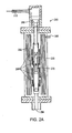
- a furnace 200 is utilized in the formation of polycrystalline source 130 incorporating a high concentration of at least one substitutional dopant.
- Furnace 200 includes a pellet loading mechanism 210, which drops pellets comprising or consisting essentially of Al into a crucible 220.
- the pellets may be doped with one or more dopant species.
- the dopant concentration in the pellets is less than 12% by weight.
- Crucible 220 includes a bottom plug 230 and a foil wrap 240.
- Bottom plug 230 may be approximately cylindrical with, e.g., a diameter of approximately 0.625 inches and a height of approximately 0.5 inches.
- Bottom plug 230 may comprise or consist essentially of tungsten (W), or another high-melting-point material inert to AlN.
- Foil wrap 240 wraps around bottom plug 230, forming a cylinder open at the top and sealed at the bottom by bottom plug 230.
- Foil wrap 240 may comprise or consist essentially of W, or another high-melting-point material inert to AlN, and may have a thickness of approximately 0.001 inch.
- foil wrap 240 may be wrapped around bottom plug 230 multiple times, e.g., a three-ply foil wrap 240 is formed by wrapping W foil around bottom plug 230 three times.
- Foil wrap 240 is held in place by at least one wire 250, which may comprise or consist essentially of a tungsten-rhenium alloy (e.g., 25% rhenium) and have a thickness of approximately 0.01 inch.
- Crucible 220 is disposed within a susceptor 260 and on top of a crucible stand 270. Both susceptor 260 and crucible stand 270 may comprise or consist essentially of W.
- a crucible funnel 280 is disposed above the top opening of crucible 220, and may comprise or consist essentially of molybdenum (Mo).
- Mo molybdenum
- Furnace 200 is resistively heated by one or more heating elements 290, which are surrounded by insulation 292. Heating elements 290 may be heated to temperatures up to approximately 2300 °C, and furnace 200 may operate at pressures up to approximately 60 bar. In an exemplary embodiment, the furnace operates at pressures up to approximately 10 bar. Generally, elevated pressures may enable the incorporation of high concentrations of dopants into polycrystalline source 130 (as described below) by limiting evaporation of the dopant species or a compound thereof. For example, when Si is utilized as a dopant, high furnace pressures may substantially prevent the evaporation of the Si in the form of Si 3 N 4 . Gas flows into furnace 200 from a bottom inlet 294 and is exhausted through a top outlet 296.
- the gas may comprise or consist essentially of nitrogen or a mixture of nitrogen and 3% hydrogen (i.e., forming gas), and is filtered by a gas filter (not shown) that reduces levels of contaminants such as oxygen, water vapor, and hydrocarbons to less than 10 parts per billion (ppb).
- An upper funnel 298 connects pellet loading mechanism 210 to crucible funnel 280.
- pellets are desirably cleaned in preparation for loading into pellet loading mechanism 210.
- the pellets are preferably all similarly sized and shaped to facilitate automatic handling (as described below).
- the pellets are sifted in order to remove oddly shaped pellets or small shavings.
- the pellets are then ultrasonically cleaned in distilled water for approximately 20 minutes.
- the pellets are immersed in a mixture of hydrofluoric acid (HF) and nitric acid (HNO 3 ) for approximately 2 minutes at room temperature.
- the pellets are rinsed in distilled water and multiple times in methanol, whereupon they may be stored in an inert atmosphere prior to loading into pellet loading mechanism 210.
- Cleaning doped or undoped Al pellets is important to produce consistent results and to provide a consistent surface oxidation (or reduced layer thereof) to the reaction for production of both doped and undoped polycrystalline source 130.
- Crucible 220 is loaded into furnace 200, and the pellets are loaded into pellet loading mechanism 210.
- a cleaning cycle in which the pellets are not dropped into crucible 220, may be run prior to an actual reaction cycle in which polycrystalline source 130 is formed.
- Furnace 200 is alternately subjected to a flow of forming gas and evacuated several times (e.g., three times).
- Heating elements 290 are heated to approximately 2200 °C, thus heating crucible 220 to approximately 1950 °C.
- Forming gas is flowed through furnace 200 at a high rate, e.g., approximately 0.25 liters per minute (1pm) in order to purge residual moisture and to reduce any W-containing components therein (which may have oxidized due to exposure to air or other sources of contamination).
- Heating elements 290 are then cooled back down to room temperature.
- a reaction cycle is then performed to form polycrystalline source 130.
- Furnace 200 is alternately subjected to a flow of nitrogen and evacuated several times (e.g., three times).
- the reaction cycle may be performed at temperatures within the range of approximately 1600 °C to approximately 2200 °C, and at pressures within the range of approximately 1 bar to approximately 60 bars. In an embodiment, the reaction cycle is performed at a pressure less than approximately 10 bar.
- heating elements 290 are heated to approximately 1800 °C (corresponding to a temperature of crucible 220 of approximately 1650 °C) and held at that temperature for approximately three hours.
- the gas flow is decreased to approximately 5 standard cubic centimeters per minute (sccm), and the pellets are dropped from pellet loading mechanism 210, through upper funnel 298 and crucible funnel 280, into crucible 220.
- the pellets may each weigh approximately 72 milligrams, and may be dropped at a rate of approximately 1 per minute.
- the pellets land on bottom plug 230 (or the portion of polycrystalline source 130 already produced thereon), melt, and react with the nitrogen gas to form polycrystalline source 130.
- Dopants present in the pellets are incorporated into polycrystalline source 130 at concentrations at least partially determined by the dopant concentration in the pellets and by the reaction kinetics.
- Very high dopant concentrations in polycrystalline source 130 may be achieved by using very high concentrations of dopant in the pellet and by suppressing dopant evaporation by increasing the nitrogen pressure in reaction furnace 200.
- Each subsequent pellet dropped from pellet loading mechanism 210 reacts and increases the size and volume of polycrystalline source 130. In an embodiment, substantially all of each pellet reacts to form polycrystalline source 130.
- polycrystalline source 130 may weigh up to approximately 80 grams, and may include low concentrations of impurities such as oxygen, boron, and transition metals such as iron. In an embodiment, an oxygen concentration (and/or concentration of other impurities) of polycrystalline source 130 is less than approximately 400 ppm by weight, and may even be less than approximately 100 ppm.
- Polycrystalline source 130 includes or consists essentially of AlN (or doped AlN) that is approximately stoichiometric, i.e., AlN that contains less than approximately 1% excess Al.
- Polycrystalline source 130 that is doped may include up to approximately 12% (by weight) of a dopant species such as a group IV element (e.g., Si or C), a group II element (e.g., Be or Mg) or a group VI element (e.g., O). After formation, polycrystalline source 130 may be immediately ready for subsequent sublimation-recondensation growth of single crystal AlN, and may be stored in an inert atmosphere in preparation therefor.
- a dopant species such as a group IV element (e.g., Si or C), a group II element (e.g., Be or Mg) or a group VI element (e.g., O).
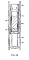
- a reactor 300 is utilized in the formation of polycrystalline source 130 consisting essentially of high purity, undoped AlN.
- Reactor 300 includes a reaction vessel 310, which is preferably fabricated of double-walled stainless steel and is water cooled.
- Reaction vessel 310 should be capable of a maximum internal gas pressure of approximately 45 pounds per square inch (psi), and may be evacuated, e.g., by a turbo pump 311 (backed by a mechanical pump 312) to approximately 10 -7 Torr.
- a feeder mechanism 320 is connected to the top of reaction vessel 310, and may be evacuated and pressurized with the same gases and pressures as reaction vessel 310. Feeder mechanism 320 may be isolated from reaction vessel 310 by an isolation valve 322.
- Pellets (which may consist essentially of high (e.g., five nines) purity undoped Al and may be shaped approximately cylindrically) released from feeder mechanism 320 are directed to a crucible 330 by an upper funnel 332 and a lower funnel 334.
- Crucible 330 includes a bottom plug 336 and a foil wrap 337.
- Bottom plug 336 may be approximately cylindrical with, e.g., a diameter of approximately 2 inches and a height of approximately 0.5 inches.
- Bottom plug 336 may comprise or consist essentially of W, or another high-melting-point material inert to AlN.
- Foil wrap 337 wraps around bottom plug 336, forming a cylinder open at the top and sealed at the bottom by bottom plug 336.
- Foil wrap 337 may comprise or consist essentially of W, or another high melting point material inert to AlN, and may have a thickness of approximately 0.001 inch.
- foil wrap 337 may be wrapped around bottom plug 336 multiple times, e.g., a three-ply foil wrap 337 is formed by wrapping W foil around bottom plug 337 three times.
- Foil wrap 337 is held in place by wire 338.
- Wire 338 may comprise or consist essentially of a tungsten-rhenium alloy (e.g., 25% rhenium) and have a thickness of approximately 0.01 inch.
- Crucible 330 is disposed within a reaction zone 340 and on top of a crucible stand 342. Both reaction zone 340 and crucible stand 342 may include or consist essentially of W. Lower funnel 334 is disposed above the top opening of crucible 330, and may comprise or consist essentially of W. Lower funnel 334 is shaped to direct pellets from feeder mechanism 320 and upper funnel 332 into crucible 330.
- Reactor 300 includes an inductive heating coil 350, which wraps around insulation 360.
- Insulation 360 may include or consist essentially of bubble alumina available from Zircar Ceramics, Inc. of Florida, New York held within a quartz holder.
- Inductive heating coil 350 may be a 10 kHz, 20 kilowatt inductive heating system available from Mesta Electronics, Inc. of N. Huntingdon, Pennsylvania, and may heat to temperatures up to approximately 2300 °C.
- An optical pyrometer port 362 enables the measurement of temperature inside the reaction zone defined by inductive heating coil 350 by pyrometry. Gas from a series of gas tanks representatively indicated at 368 flows into reactor 300 from a bottom inlet 370 and/or a top inlet 372.
- the gas may comprise or consist essentially of nitrogen or forming gas, and is filtered by a gas filter 374 that reduces levels of contaminants such as oxygen, water vapor, and hydrocarbons to less than 10 ppb.
- a vertical drive 380 is used to move crucible 330 in and out of the hot zone created by inductive heating coil 350.
- a conventional control station 390 includes electronic controls and power supplies for all of the components associated with reactor 300.
- pellets are cleaned in preparation for loading into feeder mechanism 320.
- the pellets are sifted (with or without water) in order to remove oddly shaped pellets or small shavings.
- the pellets are then ultrasonically cleaned in methanol for approximately 20 minutes, etched for approximately 7 minutes in hydrochloric acid (HCl), and rinsed several times (e.g. three times) in distilled water.
- HCl hydrochloric acid
- the pellets are immersed in a mixture of HF and HNO 3 for approximately 2 minutes at room temperature.
- the pellets are rinsed in distilled water and multiple times in methanol, whereupon they may be stored in an inert or nitrogen atmosphere prior to loading in feeder mechanism 320.
- Crucible 330 is loaded into reactor 300, and pellets are loaded into feeder mechanism 320.
- Reaction chamber 310 and feeder mechanism 320 are evacuated, e.g., to a pressure less than approximately 5 ⁇ 10 -5 Torr, and refilled with forming gas to a pressure of approximately 6 psi.
- Either nitrogen (N 2 ) gas or forming gas flows into reaction chamber 310 from bottom inlet 370 and top inlet 372 at a rate of approximately 0.25 lpm.
- the flow of gas provides a sufficient amount of nitrogen in reaction chamber 310 to convert the pellet(s) to AlN (as described below).
- Inductive heating coil 350 heats crucible 330 to approximately 1900-2200 °C, but even higher temperatures may be utilized.
- inductive heating coil 350 heats crucible 330 to approximately 2000 - 2050 °C. Temperatures in this range have been found to be sufficient to totally react the pellets into stoichiometric AlN (which includes less than approximately 1% unreacted Al) and to drive off higher vapor pressure impurities that may be trapped within polycrystalline source 130 and create optical absorptions.
- the temperature at crucible 330 may be measured by pyrometry through optical pyrometer port 362. Once crucible 330 reaches the desired temperature, the temperature and gas flow conditions within reactor 300 are held constant for an approximately 3 hour pre-soak cycle. The pre-soak cleans crucible 330 and other parts of reactor 300 of contaminants, e.g., oxides, before the introduction of the Al pellets.
- a reaction cycle is then performed to form undoped polycrystalline source 130.
- Pellets are dropped from feeder mechanism 320, through upper funnel 332 and lower funnel 334, into crucible 330.
- the pellets may each weigh approximately 0.23 gram, and may be dropped at a rate of approximately 1 every 90 seconds.
- Feeder mechanism 320 may incorporate an optical counter that counts actual pellet drops and may cycle feeder mechanism 320 to drop an additional pellet in case of a loading error.
- the pellets land on bottom plug 336 (or the portion of polycrystalline source 130 already produced thereon), melt, and react with the nitrogen gas to form undoped polycrystalline source 130.
- Each subsequent pellet dropped from feeder mechanism 320 reacts and increases the size and volume of polycrystalline source 130. In an embodiment, substantially all of each pellet reacts to form polycrystalline source 130. After a desired number of pellets are reacted to form polycrystalline source 130, the reaction gas flow rate and temperature are maintained for approximately 1 hour to ensure that the reaction is complete.
- polycrystalline source 130 may weigh up to approximately 155 grams, and consists essentially of high-purity, undoped AlN.
- an oxygen concentration (and/or concentration of other impurities such as boron or transition metals) of polycrystalline source 130 is less than approximately 400 ppm by weight, and may even be less than approximately 100 ppm.
- Polycrystalline source 130 includes or consists essentially of AlN that is approximately stoichiometric, i.e., AlN that contains less than approximately 1% excess Al. After formation, polycrystalline source 130 may be immediately ready for subsequent sublimation-recondensation growth of single crystal AlN, and may be stored in an inert atmosphere in preparation therefor.
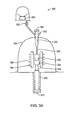
- doped or undoped polycrystalline source 130 has been fabricated by one of the techniques described above with reference to Figs. 2A and 2B and 3A-3E , it can be utilized in the sublimation-recondensation growth of single-crystal AlN as described above with reference to Fig. 1 . Because polycrystalline source 130 is approximately stoichiometric AlN with low concentrations of impurities, it may be used to form AlN crystal 120 without further preparation. Polycrystalline source 130 is separated from bottom plug 230 (or bottom plug 336), but foil wrap 240 (or foil wrap 337) remains proximate and in contact with polycrystalline source 130. Foil wrap 240 (or foil wrap 337) may remain in contact with polycrystalline source 130 and placed in crystal growth enclosure 100.
- foil wrap 240 (or foil wrap 337) is formed of W or other material inert to AlN, it does not react with or contaminate AlN crystal 120 during its formation.
- polycrystalline source 130, surrounded by foil wrap 240 (or foil wrap 337) may be broken into smaller pieces, and one or more of them may be utilized separately to form AlN crystal 120.
- pieces of foil wrap 240 (or foil wrap 337) may remain in contact with the pieces of polycrystalline source 130.
- foil wrap 240 (or foil wrap 337) may be formed of the same material as crystal growth enclosure 100, e.g., W.
- wafer 400 may be separated from AlN crystal 120 by the use of, e.g., a diamond annular saw or a wire saw.
- a crystalline orientation of wafer 400 may be within approximately 2° of the (0001) face (i.e., the c-face).
- Such c-face wafers may have an Al-polarity surface or an N-polarity surface, and may subsequently be prepared as described in U.S. Patent No. 7,037,838 or U.S. Patent Application Serial No. 11/448,595 , the entire disclosures of which are hereby incorporated by reference.
- wafer 400 may be oriented within approximately 2° of an m-face or a-face orientation (thus having a non-polar orientation) or may have a semi-polar orientation if AlN crystal 120 is cut along a different direction.
- the surfaces of these wafers may also be prepared as described in U.S. Patent No. 7,037,838 .
- Wafer 400 may have a roughly circular cross-sectional area with a diameter of greater than approximately 2 cm.
- a surface area of wafer 400 may be greater than approximately 1 cm 2 , or even greater than approximately 3 cm 2 , and may be shaped like a quadrilateral or other polygon.
- a thickness of wafer 400 may be greater than approximately 100 ⁇ m, greater than approximately 200 ⁇ m, or even greater than approximately 2 mm.
- Wafer 400 preferably has the properties of AlN crystal 120, as described herein.
- AlN crystal 120 and wafer 400 may both incorporate the dopant species at a concentration greater than approximately 10 16 /cm 3 .
- AlN crystal 120 and/or wafer 400 may exhibit n-type or p-type conductivity.
- an oxygen concentration (and/or concentration of other impurities such as boron or transition metals such as iron) of AlN crystal 120 and/or wafer 400 is less than approximately 400 parts per million by weight (ppm), and may even be less than approximately 100 ppm.
- the oxygen concentration may also be less than approximately 4.5 ⁇ 10 19 /cm 3 , or even less than 1 ⁇ 10 19 /cm 3 , as measured by dynamic SIMS.
- a conductivity of AlN crystal 120 and/or wafer 400 at room temperature may be greater than approximately 10 -4 ⁇ -1 cm -1 , or even greater than approximately 10 -2 ⁇ -1 cm -1 .
- a thermal conductivity of AlN crystal 120 and/or wafer 400 may be greater than approximately 250 Watts per meter-Kelvin (W/m ⁇ K), a value preferably measured by the American Society for Testing and Materials (ASTM) Standard E1461-01 (Current Industry Standard Test Method for Thermal Diffusivity of Solids by the Laser Flash Method), and provided by a commercial vendor such as NETZSCH Inc. of Exton, Pennsylvania.
- W/m ⁇ K Watts per meter-Kelvin
- ASTM American Society for Testing and Materials
- E1461-01 Current Industry Standard Test Method for Thermal Diffusivity of Solids by the Laser Flash Method
- NETZSCH Inc. Current Industry Standard Test Method for Thermal Diffusivity of Solids by the Laser Flash Method
- the low oxygen content of AlN crystal 120 and wafer 400 may enable an optical absorption coefficient of less than 100 /cm at a wavelength of 280 nm, as absorption at this wavelength has been ascribed to oxygen contamination (see, for example, G.A. Slack, L.J. Schowalter, D. Morelli, J.A. Freitas Jr., J. Crystal Growth 246, 287 (2002 ), the entire disclosure of which is hereby incorporated by reference).
- the AlN evaporates congruently as Al atoms and N 2 molecules with very small traces of Al 2 and AlN vapor molecules. If there is any Si 3 N 4 in the source, then, at a temperature of 2300°C that is typically used for growing AlN, the nitrogen pressure over Si 3 N 4 solid is 53 bars.
- the decomposition pressure of solid Si 3 N 4 is substantially higher than that of solid AlN.
- the Si vapor pressure is much reduced.
- the N 2 pressure over the AlN is typically kept between 0.5 and 10 bar, with 1.2 bar being preferred. This nitrogen pressure is much less than the N 2 pressure of 53 bars needed to form solid Si 3 N 4 . Thus, no Si 3 N 4 is formed under these conditions.
- the Si atoms are transported to the growing Al crystal as mostly Si 1 atoms (over 80%) although some transport may be expected as SiN, Si 2 N, Si 2 and Si 3 gas-phase molecules.
- Undoped AlN will grow very close to stoichiometric.
- the nitrogen vacancy (V N ) concentration depends on the growth temperature and the nitrogen pressure; for growth at 2300 °C, the aluminum nitride grows as Al 1 N 1-y (V N ) y , where y may be ⁇ 10 -4 at 1 bar N 2 .
- this material may be used to grow crystals by the evaporation-recondensation or solid-gas-solid technique.
- Tungsten crucibles are typically employed for growing AlN; as explained herein, the same crucibles may be used for growing Si-doped AlN crystals if the nitrogen pressure is between 0.5 to 10 bar and the temperature is 2000°C to 2300°C.
- the Si-W system possesses two intermediate compounds: WSi 2 (melting point (m.p.) 2160°C) and W 5 Si 3 (m.p. 2320°C).
- the partial pressure of Si in the gas phase is preferably maintained low enough to prevent the formulation of these phases at the growth temperature. For Si/Al ratios of up to 0.1 (10%), substantially no reaction of Si with the tungsten should occur although there may be some absorption of Si by a tungsten crucible.
- a crucible constructed of an alternative material. See, e.g., G.A. Slack, J. Whitlock, K. Morgan, and L.J. Schowalter, Mat. Res. Soc. Proc. 798, Y10.74.1 (2004 ), the entire disclosure of which is hereby incorporated by reference.
- a TaC crucible prepared as described in U.S. Patent Application Serial No.
- the doped AlN crystal is grown under conditions which generate nitrogen vacancies as described above.
- Crystal growth enclosure 100 may be made from W, but alternative crucible materials, such as TaC, may be preferred to reduce the loss of dopant (e.g., Si) through its walls.
- Annealing treatments may be employed as a means of controlling the nitrogen vacancy content, aluminum vacancy content, and/or dopant electrical activation in wafer 400 cut from AlN crystal 120.
- Exemplary AlN crystal 120 doped with Si is grown at nitrogen pressures between 0.5 and 10 bars; lower N 2 pressures may significantly slow the growth rate or suppress it entirely. Once grown, however, some of the nitrogen may be extracted from AlN crystal 120 or wafer 400, i.e., nitrogen vacancies may be injected into the material.
- Wafer 400 may be annealed at a temperature greater than approximately 1900°C in order to electrically activate a dopant species therein. The annealing may also decrease a concentration of Al vacancies and/or increase a concentration of N vacancies in wafer 400.
- a suitable N 2 pressure at temperature T for creating the maximum number of N vacancies is greater than the pressure required to form AlN from Al at the same temperature T.
- a suitable N 2 pressure used during annealing may be selected from the range of approximately 2 millibar (mbar) to approximately 0.5 bar.
- the N 2 pressure may be less than approximately twice a N 2 pressure required to form AlN from Al at temperature T.
- the N 2 pressure used during annealing is selected from the range of approximately 0.1 mbar and approximately 5 bars. Higher pressures may generally be preferred at higher temperatures.
- an inert gas such as argon (Ar) is introduced during the annealing to suppress Al evaporation as discussed below.
- Ar argon
- the Al vacancies and nitrogen vacancies can combine and be replaced by lattice voids or surface pits and the chemical composition becomes: Al 1-x Si x N 1
- Si is now present as SiN and is thus electrically active as a donor. When it was present as Si 3 N 4 , it was electrically inactive. After annealing, substantially all of a dopant species (such as Si) present in wafer 400 may be electrically activated.
- a conductivity of annealed wafer 400 may be greater than approximately 10 -4 ⁇ -1 cm -1 , or even greater than approximately 10 -2 ⁇ -1 cm -1 , at room temperature.
- Annealing may generate enough nitrogen vacancies in undoped AlN so that the electron donors are the excess Al atoms.
- one may anneal undoped wafer 400 in a low N 2 gas pressure at temperatures between 1700°C and 2200°C. During the anneal, some of the nitrogen in the AlN will diffuse out to the surface and escape, leaving the Al behind. This is preferably done in a flowing argon-nitrogen atmosphere at a total pressure within the range of approximately 2 bars to approximately 30 bars. The argon prevents the Al from evaporating.
- the nitrogen pressure is just enough to keep the AlN from converting back to metallic aluminum. That is, the pressure of N 2 is greater than the N 2 pressure required to form AlN from Al at the anneal temperature.
- Annealed undoped wafer 400 may have a conductivity greater than approximately 10 -2 ⁇ -1 cm -1 at room temperature. Such conductivity may be supplied by excess Al atoms (equivalently, by nitrogen vacancies) in the AlN lattice.
Landscapes
- Chemical & Material Sciences (AREA)
- Engineering & Computer Science (AREA)
- Organic Chemistry (AREA)
- Materials Engineering (AREA)
- Ceramic Engineering (AREA)
- Inorganic Chemistry (AREA)
- Manufacturing & Machinery (AREA)
- Crystallography & Structural Chemistry (AREA)
- Metallurgy (AREA)
- Structural Engineering (AREA)
- Chemical Kinetics & Catalysis (AREA)
- Physics & Mathematics (AREA)
- Thermal Sciences (AREA)
- Crystals, And After-Treatments Of Crystals (AREA)
- Ceramic Products (AREA)
Applications Claiming Priority (3)
| Application Number | Priority Date | Filing Date | Title |
|---|---|---|---|
| US78739906P | 2006-03-30 | 2006-03-30 | |
| PCT/US2007/007980 WO2007123735A1 (fr) | 2006-03-30 | 2007-03-30 | Procédé de dopage réglable de cristaux massifs de nitrure d'aluminium |
| EP07774299.7A EP2007933B1 (fr) | 2006-03-30 | 2007-03-30 | Procédé de dopage réglable de cristaux massifs de nitrure d'aluminium |
Related Parent Applications (2)
| Application Number | Title | Priority Date | Filing Date |
|---|---|---|---|
| EP07774299.7A Division EP2007933B1 (fr) | 2006-03-30 | 2007-03-30 | Procédé de dopage réglable de cristaux massifs de nitrure d'aluminium |
| EP07774299.7A Division-Into EP2007933B1 (fr) | 2006-03-30 | 2007-03-30 | Procédé de dopage réglable de cristaux massifs de nitrure d'aluminium |
Publications (3)
| Publication Number | Publication Date |
|---|---|
| EP2918708A2 true EP2918708A2 (fr) | 2015-09-16 |
| EP2918708A3 EP2918708A3 (fr) | 2016-01-06 |
| EP2918708B1 EP2918708B1 (fr) | 2019-10-30 |
Family
ID=38512410
Family Applications (2)
| Application Number | Title | Priority Date | Filing Date |
|---|---|---|---|
| EP15154002.8A Active EP2918708B1 (fr) | 2006-03-30 | 2007-03-30 | Procédé de recuit de tranche de nitrure d'aluminium |
| EP07774299.7A Not-in-force EP2007933B1 (fr) | 2006-03-30 | 2007-03-30 | Procédé de dopage réglable de cristaux massifs de nitrure d'aluminium |
Family Applications After (1)
| Application Number | Title | Priority Date | Filing Date |
|---|---|---|---|
| EP07774299.7A Not-in-force EP2007933B1 (fr) | 2006-03-30 | 2007-03-30 | Procédé de dopage réglable de cristaux massifs de nitrure d'aluminium |
Country Status (5)
| Country | Link |
|---|---|
| US (1) | US8012257B2 (fr) |
| EP (2) | EP2918708B1 (fr) |
| JP (1) | JP5479888B2 (fr) |
| CN (1) | CN101454487B (fr) |
| WO (1) | WO2007123735A1 (fr) |
Families Citing this family (44)
| Publication number | Priority date | Publication date | Assignee | Title |
|---|---|---|---|---|
| US20060005763A1 (en) | 2001-12-24 | 2006-01-12 | Crystal Is, Inc. | Method and apparatus for producing large, single-crystals of aluminum nitride |
| US7638346B2 (en) | 2001-12-24 | 2009-12-29 | Crystal Is, Inc. | Nitride semiconductor heterostructures and related methods |
| US8545629B2 (en) | 2001-12-24 | 2013-10-01 | Crystal Is, Inc. | Method and apparatus for producing large, single-crystals of aluminum nitride |
| WO2007065018A2 (fr) | 2005-12-02 | 2007-06-07 | Crystal Is, Inc. | Cristaux de nitrure d'aluminium dope, procede de production de ces derniers |
| US9034103B2 (en) | 2006-03-30 | 2015-05-19 | Crystal Is, Inc. | Aluminum nitride bulk crystals having high transparency to ultraviolet light and methods of forming them |
| US9771666B2 (en) | 2007-01-17 | 2017-09-26 | Crystal Is, Inc. | Defect reduction in seeded aluminum nitride crystal growth |
| US9028612B2 (en) | 2010-06-30 | 2015-05-12 | Crystal Is, Inc. | Growth of large aluminum nitride single crystals with thermal-gradient control |
| WO2008088838A1 (fr) | 2007-01-17 | 2008-07-24 | Crystal Is, Inc. | Réduction des défauts de croissance de cristaux de nitrure d'aluminium ensemencés |
| US8080833B2 (en) | 2007-01-26 | 2011-12-20 | Crystal Is, Inc. | Thick pseudomorphic nitride epitaxial layers |
| WO2008094464A2 (fr) | 2007-01-26 | 2008-08-07 | Crystal Is, Inc. | Couches épitaxiales épaisses de nitrures pseudomorphes |
| US8088220B2 (en) * | 2007-05-24 | 2012-01-03 | Crystal Is, Inc. | Deep-eutectic melt growth of nitride crystals |
| JP5303941B2 (ja) * | 2008-01-31 | 2013-10-02 | 住友電気工業株式会社 | AlxGa1−xN単結晶の成長方法 |
| WO2010001804A1 (fr) * | 2008-07-01 | 2010-01-07 | 住友電気工業株式会社 | Procédé de production d'un monocristal d'alxga(1-x)n, monocristal d'alxga(1‑x)n et optiques |
| EP2309040A4 (fr) * | 2008-07-01 | 2014-08-13 | Sumitomo Electric Industries | Procédé de producion d'un monocristal d'alxga (1-x)n, monocristal d'alxga (1-x)n et lentilles optiques |
| JP5446622B2 (ja) | 2009-06-29 | 2014-03-19 | 住友電気工業株式会社 | Iii族窒化物結晶およびその製造方法 |
| EP2595940B1 (fr) | 2010-07-20 | 2019-11-13 | Hexatech Inc. | Boule en nitrure d'aluminium polycristallin et procédé de production d'un matériau en nitrure d'aluminium polycristallin |
| WO2012056928A1 (fr) * | 2010-10-29 | 2012-05-03 | 株式会社トクヤマ | Procédé pour la fabrication d'élément optique |
| EP2639345A4 (fr) * | 2010-11-10 | 2014-04-16 | Fujikura Ltd | Appareil et procédé de production de monocristal de nitrure d'aluminium |
| JP2014507363A (ja) | 2010-12-14 | 2014-03-27 | ヘクサテック,インコーポレイテッド | 多結晶質窒化アルミニウム焼結体の熱膨張処理、および半導体製造へのその応用 |
| CN102776568B (zh) * | 2011-05-13 | 2015-09-16 | 中国科学院物理研究所 | 一种激光晶体及其制备方法和用途 |
| US8399367B2 (en) * | 2011-06-28 | 2013-03-19 | Nitride Solutions, Inc. | Process for high-pressure nitrogen annealing of metal nitrides |
| RU2469433C1 (ru) * | 2011-07-13 | 2012-12-10 | Юрий Георгиевич Шретер | Способ лазерного отделения эпитаксиальной пленки или слоя эпитаксиальной пленки от ростовой подложки эпитаксиальной полупроводниковой структуры (варианты) |
| US8962359B2 (en) | 2011-07-19 | 2015-02-24 | Crystal Is, Inc. | Photon extraction from nitride ultraviolet light-emitting devices |
| WO2014031119A1 (fr) | 2012-08-23 | 2014-02-27 | National University Corporation Tokyo University Of Agriculture And Technology | Couches de nitrure d'aluminium monocristallin à haute transparence et dispositifs formés à partir de celles-ci |
| EP2951869A1 (fr) | 2013-01-29 | 2015-12-09 | Hexatech Inc. | Dispositifs optoélectroniques incorporant un substrat monocristallin de nitrure d'aluminium |
| EP2973719B1 (fr) | 2013-03-14 | 2021-04-21 | Hexatech Inc. | Dispositifs à semiconducteur de puissance incorporant un substrat de nitrure d'aluminium monocristallin |
| WO2014151264A1 (fr) | 2013-03-15 | 2014-09-25 | Crystal Is, Inc. | Contacts planaires pour des dispositifs électroniques et optoélectroniques pseudomorphes |
| US20160284545A1 (en) * | 2015-03-25 | 2016-09-29 | Hexatech, Inc. | System and method for producing polycrystalline group iii nitride articles and use thereof in production of single crystal group iii nitride articles |
| CN108140695B (zh) | 2015-09-17 | 2021-02-09 | 晶体公司 | 包含二维空穴气体的紫外发光器件 |
| WO2017134779A1 (fr) * | 2016-02-03 | 2017-08-10 | イーメックス株式会社 | Film mince de nitrure d'aluminium, procédé de formation d'un film mince de nitrure d'aluminium, et matériau d'électrode |
| EP3434816A4 (fr) | 2016-03-23 | 2019-10-30 | Tokuyama Corporation | Procédé de fabrication d'un substrat de cristal unique de nitrure d'aluminium |
| WO2018232080A1 (fr) * | 2017-06-16 | 2018-12-20 | Crystal Is. Inc. | Croissance par ensemencement en deux étapes de monocristaux de nitrure d'aluminium de grande taille |
| CN110998886B (zh) * | 2017-07-07 | 2023-09-26 | 天工方案公司 | 用于改进的声波滤波器的取代氮化铝 |
| DE112018005414T5 (de) | 2017-11-10 | 2020-07-09 | Crystal Is, Inc. | Große, UV-Transparente Aluminiumnitrid-Einkristalle und Verfahren zu ihrer Herstellung |
| CN112567079B (zh) | 2018-06-19 | 2023-12-26 | 晶化成半导体公司 | 深紫外透明的氮化铝晶体及其形成方法 |
| CN109023513B (zh) * | 2018-08-20 | 2020-12-01 | 深圳大学 | 制备氮化铝晶体的坩埚设备及方法 |
| CN109632855B (zh) * | 2018-11-15 | 2020-05-05 | 北京大学 | 化合物半导体中替代阳离子位置的杂质缺陷浓度的检测方法 |
| CN112593293A (zh) * | 2020-11-04 | 2021-04-02 | 奥趋光电技术(杭州)有限公司 | 一种氮化铝晶片热处理方法 |
| CN112979335B (zh) * | 2021-02-08 | 2022-07-01 | 哈尔滨化兴软控科技有限公司 | 氮化铝多孔隙原料的制备方法 |
| CN113471060B (zh) * | 2021-05-27 | 2022-09-09 | 南昌大学 | 一种减少硅衬底上AlN薄膜微孔洞的制备方法 |
| CN113668061B (zh) * | 2021-07-27 | 2023-02-03 | 奥趋光电技术(杭州)有限公司 | 一种提高氮化铝晶片紫外透过率的方法 |
| WO2023168139A2 (fr) * | 2022-01-11 | 2023-09-07 | Georgia Tech Research Corporation | Dispositifs haute puissance à base de nitrure d'aluminium et procédés pour les fabriquer |
| CN116143085B (zh) * | 2022-12-26 | 2024-08-30 | 奥趋光电技术(杭州)有限公司 | 一种高纯氮化铝原料的制备方法 |
| CN118183641B (zh) * | 2024-04-16 | 2026-04-28 | 南京大学 | 一种降低AlN表面分解的高温退火方法 |
Citations (2)
| Publication number | Priority date | Publication date | Assignee | Title |
|---|---|---|---|---|
| US6719843B2 (en) | 2001-09-21 | 2004-04-13 | Crystal Is, Inc. | Powder metallurgy tungsten crucible for aluminum nitride crystal growth |
| US7037838B2 (en) | 2001-11-20 | 2006-05-02 | Rensselaer Polytechnic Institute | Method for polishing a substrate surface |
Family Cites Families (158)
| Publication number | Priority date | Publication date | Assignee | Title |
|---|---|---|---|---|
| NL6615059A (fr) | 1966-10-25 | 1968-04-26 | ||
| US3600701A (en) | 1968-03-14 | 1971-08-17 | Gen Electric | Signal generator for producing a set of signals at baseband frequency and with adjustable phase slope |
| US3531245A (en) | 1968-04-01 | 1970-09-29 | Du Pont | Magnesium-aluminum nitrides |
| US3607014A (en) | 1968-12-09 | 1971-09-21 | Dow Chemical Co | Method for preparing aluminum nitride and metal fluoride single crystals |
| US3603414A (en) | 1970-01-30 | 1971-09-07 | Frank E Stebley | Insert for drilling unit |
| US3768983A (en) | 1971-11-03 | 1973-10-30 | North American Rockwell | Single crystal beryllium oxide growth from calcium oxide-beryllium oxide melts |
| US3903357A (en) | 1971-12-06 | 1975-09-02 | Westinghouse Electric Corp | Adaptive gate video gray level measurement and tracker |
| FR2225207B1 (fr) | 1973-04-16 | 1978-04-21 | Ibm | |
| US3933573A (en) | 1973-11-27 | 1976-01-20 | The United States Of America As Represented By The Secretary Of The Air Force | Aluminum nitride single crystal growth from a molten mixture with calcium nitride |
| US4008851A (en) | 1976-01-16 | 1977-02-22 | Curt G. Joa, Inc. | Adhesive tape bag closure |
| DE2750607A1 (de) | 1977-11-11 | 1979-05-17 | Max Planck Gesellschaft | Luftbestaendiges kristallines lithiumnitrid, verfahren zu seiner herstellung und seine verwendung |
| US4547471A (en) | 1983-11-18 | 1985-10-15 | General Electric Company | High thermal conductivity aluminum nitride ceramic body |
| US5087949A (en) | 1989-06-27 | 1992-02-11 | Hewlett-Packard Company | Light-emitting diode with diagonal faces |
| US5292487A (en) | 1991-04-16 | 1994-03-08 | Sumitomo Electric Industries, Ltd. | Czochralski method using a member for intercepting radiation from raw material molten solution and apparatus therefor |
| US5578839A (en) | 1992-11-20 | 1996-11-26 | Nichia Chemical Industries, Ltd. | Light-emitting gallium nitride-based compound semiconductor device |
| JP2875726B2 (ja) | 1993-10-28 | 1999-03-31 | 新日本無線株式会社 | 化合物半導体の熱処理方法 |
| US6083812A (en) | 1993-02-02 | 2000-07-04 | Texas Instruments Incorporated | Heteroepitaxy by large surface steps |
| US5520785A (en) * | 1994-01-04 | 1996-05-28 | Motorola, Inc. | Method for enhancing aluminum nitride |
| US5525320A (en) * | 1994-07-11 | 1996-06-11 | University Of Cincinnati | Process for aluminum nitride powder production |
| JPH0859386A (ja) | 1994-08-22 | 1996-03-05 | Mitsubishi Materials Corp | 半導体単結晶育成装置 |
| US5670798A (en) | 1995-03-29 | 1997-09-23 | North Carolina State University | Integrated heterostructures of Group III-V nitride semiconductor materials including epitaxial ohmic contact non-nitride buffer layer and methods of fabricating same |
| US5981980A (en) | 1996-04-22 | 1999-11-09 | Sony Corporation | Semiconductor laminating structure |
| JP3876473B2 (ja) | 1996-06-04 | 2007-01-31 | 住友電気工業株式会社 | 窒化物単結晶及びその製造方法 |
| JP3644191B2 (ja) | 1996-06-25 | 2005-04-27 | 住友電気工業株式会社 | 半導体素子 |
| US5954874A (en) | 1996-10-17 | 1999-09-21 | Hunter; Charles Eric | Growth of bulk single crystals of aluminum nitride from a melt |
| US5858086A (en) | 1996-10-17 | 1999-01-12 | Hunter; Charles Eric | Growth of bulk single crystals of aluminum nitride |
| US5868837A (en) | 1997-01-17 | 1999-02-09 | Cornell Research Foundation, Inc. | Low temperature method of preparing GaN single crystals |
| JP3239787B2 (ja) | 1997-01-30 | 2001-12-17 | 安藤電気株式会社 | Icソケット |
| US6229160B1 (en) | 1997-06-03 | 2001-05-08 | Lumileds Lighting, U.S., Llc | Light extraction from a semiconductor light-emitting device via chip shaping |
| US6270569B1 (en) | 1997-06-11 | 2001-08-07 | Hitachi Cable Ltd. | Method of fabricating nitride crystal, mixture, liquid phase growth method, nitride crystal, nitride crystal powders, and vapor phase growth method |
| JP3776565B2 (ja) | 1997-06-12 | 2006-05-17 | 株式会社コトブキ | 伸縮式階段状観覧席 |
| US6006620A (en) | 1997-12-01 | 1999-12-28 | Chrysler Corporation | Automated manual transmission controller |
| WO1999034037A1 (fr) | 1997-12-25 | 1999-07-08 | Japan Energy Corporation | Procede de preparation de monocristaux de composes semi-conducteurs, equipement pour ce procede et monocristaux de composes semi-conducteurs |
| US6091085A (en) | 1998-02-19 | 2000-07-18 | Agilent Technologies, Inc. | GaN LEDs with improved output coupling efficiency |
| JP4214585B2 (ja) | 1998-04-24 | 2009-01-28 | 富士ゼロックス株式会社 | 半導体デバイス、半導体デバイスの製造方法及び製造装置 |
| JP3439994B2 (ja) * | 1998-07-07 | 2003-08-25 | 科学技術振興事業団 | 低抵抗n型および低抵抗p型単結晶AlN薄膜の合成法 |
| US6045612A (en) | 1998-07-07 | 2000-04-04 | Cree, Inc. | Growth of bulk single crystals of aluminum nitride |
| KR100277968B1 (ko) | 1998-09-23 | 2001-03-02 | 구자홍 | 질화갈륨 기판 제조방법 |
| US6063185A (en) | 1998-10-09 | 2000-05-16 | Cree, Inc. | Production of bulk single crystals of aluminum nitride, silicon carbide and aluminum nitride: silicon carbide alloy |
| US6086672A (en) | 1998-10-09 | 2000-07-11 | Cree, Inc. | Growth of bulk single crystals of aluminum nitride: silicon carbide alloys |
| US6048813A (en) | 1998-10-09 | 2000-04-11 | Cree, Inc. | Simulated diamond gemstones formed of aluminum nitride and aluminum nitride: silicon carbide alloys |
| US6404125B1 (en) | 1998-10-21 | 2002-06-11 | Sarnoff Corporation | Method and apparatus for performing wavelength-conversion using phosphors with light emitting diodes |
| JP3015887B1 (ja) | 1998-11-19 | 2000-03-06 | 科学技術庁金属材料技術研究所長 | バルク単結晶育成方法 |
| JP3062688B2 (ja) * | 1998-12-17 | 2000-07-12 | ファインセラミックス技術研究組合 | 高熱伝導窒化アルミニウム焼結体の製造方法 |
| US6187089B1 (en) | 1999-02-05 | 2001-02-13 | Memc Electronic Materials, Inc. | Tungsten doped crucible and method for preparing same |
| US6592663B1 (en) | 1999-06-09 | 2003-07-15 | Ricoh Company Ltd. | Production of a GaN bulk crystal substrate and a semiconductor device formed on a GaN bulk crystal substrate |
| US6829273B2 (en) | 1999-07-16 | 2004-12-07 | Agilent Technologies, Inc. | Nitride semiconductor layer structure and a nitride semiconductor laser incorporating a portion of same |
| RU2158789C1 (ru) | 1999-08-04 | 2000-11-10 | Водаков Юрий Александрович | Способ эпитаксиального выращивания монокристаллического нитрида алюминия и ростовая камера для осуществления способа |
| JP4145437B2 (ja) | 1999-09-28 | 2008-09-03 | 住友電気工業株式会社 | 単結晶GaNの結晶成長方法及び単結晶GaN基板の製造方法と単結晶GaN基板 |
| US6398867B1 (en) | 1999-10-06 | 2002-06-04 | General Electric Company | Crystalline gallium nitride and method for forming crystalline gallium nitride |
| US6350393B2 (en) | 1999-11-04 | 2002-02-26 | Cabot Microelectronics Corporation | Use of CsOH in a dielectric CMP slurry |
| JP2001192647A (ja) | 2000-01-14 | 2001-07-17 | Seimi Chem Co Ltd | 酸化セリウム含有研磨用組成物及び研磨方法 |
| US6879615B2 (en) | 2000-01-19 | 2005-04-12 | Joseph Reid Henrichs | FCSEL that frequency doubles its output emissions using sum-frequency generation |
| US6698647B1 (en) * | 2000-03-10 | 2004-03-02 | Honeywell International Inc. | Aluminum-comprising target/backing plate structures |
| US6447604B1 (en) | 2000-03-13 | 2002-09-10 | Advanced Technology Materials, Inc. | Method for achieving improved epitaxy quality (surface texture and defect density) on free-standing (aluminum, indium, gallium) nitride ((al,in,ga)n) substrates for opto-electronic and electronic devices |
| US6596079B1 (en) | 2000-03-13 | 2003-07-22 | Advanced Technology Materials, Inc. | III-V nitride substrate boule and method of making and using the same |
| US6777717B1 (en) | 2000-09-21 | 2004-08-17 | Gelcore, Llc | LED reflector for improved light extraction |
| US7053413B2 (en) | 2000-10-23 | 2006-05-30 | General Electric Company | Homoepitaxial gallium-nitride-based light emitting device and method for producing |
| JP2002222771A (ja) | 2000-11-21 | 2002-08-09 | Ngk Insulators Ltd | Iii族窒化物膜の製造方法、iii族窒化物膜の製造用下地膜、及びその下地膜の製造方法 |
| US6791119B2 (en) | 2001-02-01 | 2004-09-14 | Cree, Inc. | Light emitting diodes including modifications for light extraction |
| US7233028B2 (en) | 2001-02-23 | 2007-06-19 | Nitronex Corporation | Gallium nitride material devices and methods of forming the same |
| US6488767B1 (en) | 2001-06-08 | 2002-12-03 | Advanced Technology Materials, Inc. | High surface quality GaN wafer and method of fabricating same |
| US6936357B2 (en) | 2001-07-06 | 2005-08-30 | Technologies And Devices International, Inc. | Bulk GaN and ALGaN single crystals |
| US7501023B2 (en) * | 2001-07-06 | 2009-03-10 | Technologies And Devices, International, Inc. | Method and apparatus for fabricating crack-free Group III nitride semiconductor materials |
| US7067849B2 (en) | 2001-07-17 | 2006-06-27 | Lg Electronics Inc. | Diode having high brightness and method thereof |
| EP1416219B1 (fr) | 2001-08-09 | 2016-06-22 | Everlight Electronics Co., Ltd | Illuminateur del et source lumineuse d'eclairage del de type carte |
| JP3785970B2 (ja) | 2001-09-03 | 2006-06-14 | 日本電気株式会社 | Iii族窒化物半導体素子の製造方法 |
| EP1436844B1 (fr) | 2001-09-05 | 2016-03-23 | Rensselaer Polytechnic Institute | Nanoparticules passivees, leur procede de production et dispositifs integrant lesdites nanoparticules |
| US7105865B2 (en) | 2001-09-19 | 2006-09-12 | Sumitomo Electric Industries, Ltd. | AlxInyGa1−x−yN mixture crystal substrate |
| US7211146B2 (en) | 2001-09-21 | 2007-05-01 | Crystal Is, Inc. | Powder metallurgy crucible for aluminum nitride crystal growth |
| US6515308B1 (en) | 2001-12-21 | 2003-02-04 | Xerox Corporation | Nitride-based VCSEL or light emitting diode with p-n tunnel junction current injection |
| US20060005763A1 (en) | 2001-12-24 | 2006-01-12 | Crystal Is, Inc. | Method and apparatus for producing large, single-crystals of aluminum nitride |
| US8545629B2 (en) | 2001-12-24 | 2013-10-01 | Crystal Is, Inc. | Method and apparatus for producing large, single-crystals of aluminum nitride |
| US7638346B2 (en) | 2001-12-24 | 2009-12-29 | Crystal Is, Inc. | Nitride semiconductor heterostructures and related methods |
| US6770135B2 (en) | 2001-12-24 | 2004-08-03 | Crystal Is, Inc. | Method and apparatus for producing large, single-crystals of aluminum nitride |
| JP3782357B2 (ja) | 2002-01-18 | 2006-06-07 | 株式会社東芝 | 半導体発光素子の製造方法 |
| US7063741B2 (en) | 2002-03-27 | 2006-06-20 | General Electric Company | High pressure high temperature growth of crystalline group III metal nitrides |
| US6841001B2 (en) | 2002-07-19 | 2005-01-11 | Cree, Inc. | Strain compensated semiconductor structures and methods of fabricating strain compensated semiconductor structures |
| EP2290715B1 (fr) | 2002-08-01 | 2019-01-23 | Nichia Corporation | Dispositif semi-conducteur à luminescence, procédé de fabrication de ce dernier et appareil à luminescence comprenant ce dispositif |
| DE10248964B4 (de) * | 2002-10-14 | 2011-12-01 | Crystal-N Gmbh | Verfahren zur Sublimationszüchtung von Aluminiumnitrid-Einkristallen |
| AU2003285769A1 (en) | 2002-12-11 | 2004-06-30 | Ammono Sp. Z O.O. | A substrate for epitaxy and a method of preparing the same |
| US7186302B2 (en) | 2002-12-16 | 2007-03-06 | The Regents Of The University Of California | Fabrication of nonpolar indium gallium nitride thin films, heterostructures and devices by metalorganic chemical vapor deposition |
| JP4373086B2 (ja) | 2002-12-27 | 2009-11-25 | 株式会社半導体エネルギー研究所 | 発光装置 |
| FR2852974A1 (fr) | 2003-03-31 | 2004-10-01 | Soitec Silicon On Insulator | Procede de fabrication de cristaux monocristallins |
| US7521854B2 (en) | 2003-04-15 | 2009-04-21 | Luminus Devices, Inc. | Patterned light emitting devices and extraction efficiencies related to the same |
| US6831302B2 (en) | 2003-04-15 | 2004-12-14 | Luminus Devices, Inc. | Light emitting devices with improved extraction efficiency |
| US7211831B2 (en) | 2003-04-15 | 2007-05-01 | Luminus Devices, Inc. | Light emitting device with patterned surfaces |
| US7098589B2 (en) | 2003-04-15 | 2006-08-29 | Luminus Devices, Inc. | Light emitting devices with high light collimation |
| US7274043B2 (en) | 2003-04-15 | 2007-09-25 | Luminus Devices, Inc. | Light emitting diode systems |
| US7306748B2 (en) | 2003-04-25 | 2007-12-11 | Saint-Gobain Ceramics & Plastics, Inc. | Methods for machining ceramics |
| US7192849B2 (en) | 2003-05-07 | 2007-03-20 | Sensor Electronic Technology, Inc. | Methods of growing nitride-based film using varying pulses |
| JP4112449B2 (ja) | 2003-07-28 | 2008-07-02 | 株式会社東芝 | 放電電極及び放電灯 |
| DE10335538A1 (de) | 2003-07-31 | 2005-02-24 | Sicrystal Ag | Verfahren und Vorrichtung zur AIN-Einkristall-Herstellung mit gasdurchlässiger Tiegelwand |
| EP1658642B1 (fr) | 2003-08-28 | 2014-02-26 | Panasonic Corporation | Dispositif electroluminescent a semiconducteur, module electroluminescent, appareil d'eclairage, element d'affichage et procede de fabrication du dispositif electroluminescent a semiconducteur |
| US7288152B2 (en) | 2003-08-29 | 2007-10-30 | Matsushita Electric Industrial Co., Ltd. | Method of manufacturing GaN crystals and GaN crystal substrate, GaN crystals and GaN crystal substrate obtained by the method, and semiconductor device including the same |
| US6995402B2 (en) | 2003-10-03 | 2006-02-07 | Lumileds Lighting, U.S., Llc | Integrated reflector cup for a light emitting device mount |
| US7323256B2 (en) | 2003-11-13 | 2008-01-29 | Cree, Inc. | Large area, uniformly low dislocation density GaN substrate and process for making the same |
| US7087112B1 (en) * | 2003-12-02 | 2006-08-08 | Crystal Is, Inc. | Nitride ceramics to mount aluminum nitride seed for sublimation growth |
| DE60341314C5 (de) | 2003-12-09 | 2023-03-23 | The Regents Of The University Of California | Hocheffiziente leuchtdioden auf galliumnitridbasis mit oberflächenaufrauhung |
| US7518158B2 (en) | 2003-12-09 | 2009-04-14 | Cree, Inc. | Semiconductor light emitting devices and submounts |
| US7056383B2 (en) | 2004-02-13 | 2006-06-06 | The Fox Group, Inc. | Tantalum based crucible |
| US7569863B2 (en) | 2004-02-19 | 2009-08-04 | Panasonic Corporation | Semiconductor light emitting device |
| US7420218B2 (en) | 2004-03-18 | 2008-09-02 | Matsushita Electric Industrial Co., Ltd. | Nitride based LED with a p-type injection region |
| WO2005111278A1 (fr) | 2004-05-19 | 2005-11-24 | Sumitomo Electric Industries, Ltd. | Cristal de semi-conducteur en nitrure du groupe iii, procédé servant à produire celui-ci et dispositif semi-conducteur en nitrure du groupe iii |
| US20050269577A1 (en) | 2004-06-08 | 2005-12-08 | Matsushita Electric Industrial Co., Ltd. | Surface treatment method and surface treatment device |
| US7339205B2 (en) | 2004-06-28 | 2008-03-04 | Nitronex Corporation | Gallium nitride materials and methods associated with the same |
| US7534633B2 (en) | 2004-07-02 | 2009-05-19 | Cree, Inc. | LED with substrate modifications for enhanced light extraction and method of making same |
| US7476910B2 (en) | 2004-09-10 | 2009-01-13 | Kabushiki Kaisha Toshiba | Semiconductor light emitting device and method for manufacturing the same |
| US7906788B2 (en) | 2004-12-22 | 2011-03-15 | Panasonic Corporation | Semiconductor light emitting device, illumination module, illumination apparatus, method for manufacturing semiconductor light emitting device, and method for manufacturing semiconductor light emitting element |
| US7186580B2 (en) | 2005-01-11 | 2007-03-06 | Semileds Corporation | Light emitting diodes (LEDs) with improved light extraction by roughening |
| US7335920B2 (en) | 2005-01-24 | 2008-02-26 | Cree, Inc. | LED with current confinement structure and surface roughening |
| US7125734B2 (en) | 2005-03-09 | 2006-10-24 | Gelcore, Llc | Increased light extraction from a nitride LED |
| JP2006310721A (ja) | 2005-03-28 | 2006-11-09 | Yokohama National Univ | 自発光デバイス |
| US7678195B2 (en) | 2005-04-07 | 2010-03-16 | North Carolina State University | Seeded growth process for preparing aluminum nitride single crystals |
| US8101498B2 (en) | 2005-04-21 | 2012-01-24 | Pinnington Thomas Henry | Bonded intermediate substrate and method of making same |
| US7544963B2 (en) | 2005-04-29 | 2009-06-09 | Cree, Inc. | Binary group III-nitride based high electron mobility transistors |
| KR20060127743A (ko) | 2005-06-06 | 2006-12-13 | 스미토모덴키고교가부시키가이샤 | 질화물 반도체 기판과 그 제조 방법 |
| KR100616686B1 (ko) | 2005-06-10 | 2006-08-28 | 삼성전기주식회사 | 질화물계 반도체 장치의 제조 방법 |
| US20060288929A1 (en) | 2005-06-10 | 2006-12-28 | Crystal Is, Inc. | Polar surface preparation of nitride substrates |
| WO2006137711A1 (fr) | 2005-06-22 | 2006-12-28 | Seoul Opto-Device Co., Ltd. | Dispositif luminescent et procédé de fabrication idoine |
| TWI422044B (zh) | 2005-06-30 | 2014-01-01 | 克立公司 | 封裝發光裝置之晶片尺度方法及經晶片尺度封裝之發光裝置 |
| US20070018182A1 (en) | 2005-07-20 | 2007-01-25 | Goldeneye, Inc. | Light emitting diodes with improved light extraction and reflectivity |
| JP4778745B2 (ja) | 2005-07-27 | 2011-09-21 | パナソニック株式会社 | 半導体発光装置及びその製造方法 |
| JP2009515344A (ja) | 2005-11-04 | 2009-04-09 | ザ リージェンツ オブ ザ ユニバーシティ オブ カリフォルニア | 高い光抽出効率の発光ダイオード(led) |
| EP1960570A2 (fr) | 2005-11-28 | 2008-08-27 | Crystal Is, Inc. | Cristaux de nitrure d aluminium de taille importante a defauts reduits et procedes de fabrication de ceux-ci |
| WO2007065018A2 (fr) * | 2005-12-02 | 2007-06-07 | Crystal Is, Inc. | Cristaux de nitrure d'aluminium dope, procede de production de ces derniers |
| WO2007073001A1 (fr) | 2005-12-22 | 2007-06-28 | Showa Denko K.K. | Diode electroluminescente et son procede de fabrication |
| JP4963839B2 (ja) | 2006-02-06 | 2012-06-27 | 昭和電工株式会社 | 発光装置 |
| EP1994552B1 (fr) | 2006-03-10 | 2020-12-30 | UNM Rainforest Innovations | Croissance en deux phases de nanofils de groupe iii-v |
| US9034103B2 (en) | 2006-03-30 | 2015-05-19 | Crystal Is, Inc. | Aluminum nitride bulk crystals having high transparency to ultraviolet light and methods of forming them |
| US20080012034A1 (en) | 2006-07-17 | 2008-01-17 | 3M Innovative Properties Company | Led package with converging extractor |
| US7714340B2 (en) | 2006-09-06 | 2010-05-11 | Palo Alto Research Center Incorporated | Nitride light-emitting device |
| US7842960B2 (en) | 2006-09-06 | 2010-11-30 | Lumination Llc | Light emitting packages and methods of making same |
| US7631986B2 (en) | 2006-10-31 | 2009-12-15 | Koninklijke Philips Electronics, N.V. | Lighting device package |
| US20090121250A1 (en) | 2006-11-15 | 2009-05-14 | Denbaars Steven P | High light extraction efficiency light emitting diode (led) using glass packaging |
| US9318327B2 (en) | 2006-11-28 | 2016-04-19 | Cree, Inc. | Semiconductor devices having low threading dislocations and improved light extraction and methods of making the same |
| US8110838B2 (en) | 2006-12-08 | 2012-02-07 | Luminus Devices, Inc. | Spatial localization of light-generating portions in LEDs |
| US7687823B2 (en) | 2006-12-26 | 2010-03-30 | Nichia Corporation | Light-emitting apparatus and method of producing the same |
| WO2008088838A1 (fr) | 2007-01-17 | 2008-07-24 | Crystal Is, Inc. | Réduction des défauts de croissance de cristaux de nitrure d'aluminium ensemencés |
| WO2008094464A2 (fr) | 2007-01-26 | 2008-08-07 | Crystal Is, Inc. | Couches épitaxiales épaisses de nitrures pseudomorphes |
| US8080833B2 (en) | 2007-01-26 | 2011-12-20 | Crystal Is, Inc. | Thick pseudomorphic nitride epitaxial layers |
| US9061450B2 (en) | 2007-02-12 | 2015-06-23 | Cree, Inc. | Methods of forming packaged semiconductor light emitting devices having front contacts by compression molding |
| US8163582B2 (en) | 2007-04-23 | 2012-04-24 | Goldeneye, Inc. | Method for fabricating a light emitting diode chip including etching by a laser beam |
| US8088220B2 (en) | 2007-05-24 | 2012-01-03 | Crystal Is, Inc. | Deep-eutectic melt growth of nitride crystals |
| JP2009049395A (ja) | 2007-07-24 | 2009-03-05 | Toyoda Gosei Co Ltd | Iii族窒化物系化合物半導体発光素子 |
| US8866185B2 (en) | 2007-09-06 | 2014-10-21 | SemiLEDs Optoelectronics Co., Ltd. | White light LED with multiple encapsulation layers |
| KR20100097177A (ko) | 2007-11-30 | 2010-09-02 | 더 리전트 오브 더 유니버시티 오브 캘리포니아 | 향상된 광 출력을 가지는 질화 갈륨 기반의 얇은 발광 다이오드 |
| US20090140279A1 (en) | 2007-12-03 | 2009-06-04 | Goldeneye, Inc. | Substrate-free light emitting diode chip |
| US7713769B2 (en) | 2007-12-21 | 2010-05-11 | Tekcore Co., Ltd. | Method for fabricating light emitting diode structure having irregular serrations |
| US8049237B2 (en) | 2007-12-28 | 2011-11-01 | Nichia Corporation | Light emitting device |
| US20090173958A1 (en) | 2008-01-04 | 2009-07-09 | Cree, Inc. | Light emitting devices with high efficiency phospor structures |
| US7859000B2 (en) | 2008-04-10 | 2010-12-28 | Cree, Inc. | LEDs using single crystalline phosphor and methods of fabricating same |
| KR101092079B1 (ko) | 2008-04-24 | 2011-12-12 | 엘지이노텍 주식회사 | 반도체 발광소자 및 그 제조방법 |
| KR20100003321A (ko) | 2008-06-24 | 2010-01-08 | 삼성전자주식회사 | 발광 소자, 이를 포함하는 발광 장치, 상기 발광 소자 및발광 장치의 제조 방법 |
| US20090321758A1 (en) | 2008-06-25 | 2009-12-31 | Wen-Huang Liu | Led with improved external light extraction efficiency |
| JP5305758B2 (ja) | 2008-06-30 | 2013-10-02 | 株式会社東芝 | 半導体発光装置 |
| US8384115B2 (en) | 2008-08-01 | 2013-02-26 | Cree, Inc. | Bond pad design for enhancing light extraction from LED chips |
| US20100314551A1 (en) | 2009-06-11 | 2010-12-16 | Bettles Timothy J | In-line Fluid Treatment by UV Radiation |
-
2007
- 2007-03-30 WO PCT/US2007/007980 patent/WO2007123735A1/fr not_active Ceased
- 2007-03-30 CN CN2007800181039A patent/CN101454487B/zh active Active
- 2007-03-30 EP EP15154002.8A patent/EP2918708B1/fr active Active
- 2007-03-30 US US11/731,790 patent/US8012257B2/en active Active
- 2007-03-30 EP EP07774299.7A patent/EP2007933B1/fr not_active Not-in-force
- 2007-03-30 JP JP2009503043A patent/JP5479888B2/ja not_active Expired - Fee Related
Patent Citations (2)
| Publication number | Priority date | Publication date | Assignee | Title |
|---|---|---|---|---|
| US6719843B2 (en) | 2001-09-21 | 2004-04-13 | Crystal Is, Inc. | Powder metallurgy tungsten crucible for aluminum nitride crystal growth |
| US7037838B2 (en) | 2001-11-20 | 2006-05-02 | Rensselaer Polytechnic Institute | Method for polishing a substrate surface |
Non-Patent Citations (10)
| Title |
|---|
| C.G. VANDE WALLE ET AL., MRS INTERNET J. NITRIDE SEMICOND. RES., vol. 4S1, 1999, pages G 10.4 |
| C.G. VANDE WALLE, PHYS. REV. B, vol. 57, 1998, pages R2033 |
| G.A. SLACK; J. WHITLOCK; K. MORGAN; L.J. SCHOWALTER, MAT. RES. SOC. PROC., vol. 798, 2004 |
| G.A. SLACK; L.J. SCHOWALTER; D. MORELLI; FREITAS JR., J. CRYSTAL GROWTH, vol. 246, 2002, pages 287 |
| HERMANN ET AL., APPL. PHYS. LETTERS, vol. 86, 2005, pages 192108 |
| M. BOCKOWSKI; A. WITEK; S. KRUKOWSKI; M. WROBLEWSKI; S. POROWSKI; R.M. AYRAL-MARIN; J.C. TEDENAC, JOURNAL OF MATERIALS SYNTHESIS AND PROCESSING, vol. 5, 1997, pages 449 |
| M.W. CHASE, JR.: "NIST-JANAF Thermochemical Tables, Fourth edition", 1998, article "Journal of Physical and Chemical Reference Data" |
| R. ZEISEL ET AL., PHYS. REV. B, vol. 61, 2000, pages R16283 |
| SLACK; MCNELLY, J. CRYSTAL GROWTH, vol. 34, 1976, pages 263 |
| SLACK; MCNELLY, J. CRYSTAL GROWTH, vol. 42, 1977, pages 560 |
Also Published As
| Publication number | Publication date |
|---|---|
| EP2007933A1 (fr) | 2008-12-31 |
| US20070243653A1 (en) | 2007-10-18 |
| CN101454487B (zh) | 2013-01-23 |
| EP2918708B1 (fr) | 2019-10-30 |
| JP5479888B2 (ja) | 2014-04-23 |
| EP2007933B1 (fr) | 2017-05-10 |
| US8012257B2 (en) | 2011-09-06 |
| EP2918708A3 (fr) | 2016-01-06 |
| WO2007123735A1 (fr) | 2007-11-01 |
| JP2009532313A (ja) | 2009-09-10 |
| CN101454487A (zh) | 2009-06-10 |
Similar Documents
| Publication | Publication Date | Title |
|---|---|---|
| US10801127B2 (en) | Aluminum nitride bulk crystals having high transparency to ultraviolet light and methods of forming them | |
| EP2007933B1 (fr) | Procédé de dopage réglable de cristaux massifs de nitrure d'aluminium | |
| US8461071B2 (en) | Polycrystalline group III metal nitride with getter and method of making | |
| US11913136B2 (en) | Thermal control for formation and processing of aluminum nitride | |
| US8987156B2 (en) | Polycrystalline group III metal nitride with getter and method of making | |
| US7935382B2 (en) | Method for making crystalline composition | |
| US11168411B2 (en) | Impurity control during formation of aluminum nitride crystals and thermal treatment of aluminum nitride crystals | |
| USRE47114E1 (en) | Polycrystalline group III metal nitride with getter and method of making | |
| US20210269937A1 (en) | Silicon carbide crystals and methods for producing same | |
| US12344957B1 (en) | Tungsten-infused aluminum nitride crystals and methods of forming them | |
| US20160284545A1 (en) | System and method for producing polycrystalline group iii nitride articles and use thereof in production of single crystal group iii nitride articles |
Legal Events
| Date | Code | Title | Description |
|---|---|---|---|
| PUAI | Public reference made under article 153(3) epc to a published international application that has entered the european phase |
Free format text: ORIGINAL CODE: 0009012 |
|
| AC | Divisional application: reference to earlier application |
Ref document number: 2007933 Country of ref document: EP Kind code of ref document: P |
|
| AK | Designated contracting states |
Kind code of ref document: A2 Designated state(s): AT BE BG CH CY CZ DE DK EE ES FI FR GB GR HU IE IS IT LI LT LU LV MC MT NL PL PT RO SE SI SK TR |
|
| PUAL | Search report despatched |
Free format text: ORIGINAL CODE: 0009013 |
|
| AK | Designated contracting states |
Kind code of ref document: A3 Designated state(s): AT BE BG CH CY CZ DE DK EE ES FI FR GB GR HU IE IS IT LI LT LU LV MC MT NL PL PT RO SE SI SK TR |
|
| RIC1 | Information provided on ipc code assigned before grant |
Ipc: C30B 33/00 20060101ALI20151201BHEP Ipc: C30B 33/02 20060101ALI20151201BHEP Ipc: C30B 23/00 20060101ALI20151201BHEP Ipc: C30B 29/40 20060101AFI20151201BHEP |
|
| 17P | Request for examination filed |
Effective date: 20160704 |
|
| RBV | Designated contracting states (corrected) |
Designated state(s): AT BE BG CH CY CZ DE DK EE ES FI FR GB GR HU IE IS IT LI LT LU LV MC MT NL PL PT RO SE SI SK TR |
|
| STAA | Information on the status of an ep patent application or granted ep patent |
Free format text: STATUS: EXAMINATION IS IN PROGRESS |
|
| 17Q | First examination report despatched |
Effective date: 20171027 |
|
| GRAP | Despatch of communication of intention to grant a patent |
Free format text: ORIGINAL CODE: EPIDOSNIGR1 |
|
| STAA | Information on the status of an ep patent application or granted ep patent |
Free format text: STATUS: GRANT OF PATENT IS INTENDED |
|
| RIC1 | Information provided on ipc code assigned before grant |
Ipc: C30B 23/00 20060101ALI20190215BHEP Ipc: C01B 21/072 20060101ALI20190215BHEP Ipc: C30B 29/40 20060101AFI20190215BHEP Ipc: C30B 33/00 20060101ALI20190215BHEP Ipc: C30B 33/02 20060101ALI20190215BHEP Ipc: C04B 35/581 20060101ALI20190215BHEP Ipc: C04B 35/65 20060101ALI20190215BHEP |
|
| INTG | Intention to grant announced |
Effective date: 20190327 |
|
| GRAS | Grant fee paid |
Free format text: ORIGINAL CODE: EPIDOSNIGR3 |
|
| GRAJ | Information related to disapproval of communication of intention to grant by the applicant or resumption of examination proceedings by the epo deleted |
Free format text: ORIGINAL CODE: EPIDOSDIGR1 |
|
| GRAL | Information related to payment of fee for publishing/printing deleted |
Free format text: ORIGINAL CODE: EPIDOSDIGR3 |
|
| STAA | Information on the status of an ep patent application or granted ep patent |
Free format text: STATUS: EXAMINATION IS IN PROGRESS |
|
| INTC | Intention to grant announced (deleted) | ||
| GRAR | Information related to intention to grant a patent recorded |
Free format text: ORIGINAL CODE: EPIDOSNIGR71 |
|
| STAA | Information on the status of an ep patent application or granted ep patent |
Free format text: STATUS: GRANT OF PATENT IS INTENDED |
|
| GRAA | (expected) grant |
Free format text: ORIGINAL CODE: 0009210 |
|
| STAA | Information on the status of an ep patent application or granted ep patent |
Free format text: STATUS: THE PATENT HAS BEEN GRANTED |
|
| INTG | Intention to grant announced |
Effective date: 20190919 |
|
| AC | Divisional application: reference to earlier application |
Ref document number: 2007933 Country of ref document: EP Kind code of ref document: P |
|
| AK | Designated contracting states |
Kind code of ref document: B1 Designated state(s): AT BE BG CH CY CZ DE DK EE ES FI FR GB GR HU IE IS IT LI LT LU LV MC MT NL PL PT RO SE SI SK TR |
|
| REG | Reference to a national code |
Ref country code: GB Ref legal event code: FG4D |
|
| REG | Reference to a national code |
Ref country code: CH Ref legal event code: EP |
|
| REG | Reference to a national code |
Ref country code: AT Ref legal event code: REF Ref document number: 1196233 Country of ref document: AT Kind code of ref document: T Effective date: 20191115 |
|
| REG | Reference to a national code |
Ref country code: DE Ref legal event code: R096 Ref document number: 602007059445 Country of ref document: DE |
|
| REG | Reference to a national code |
Ref country code: IE Ref legal event code: FG4D |
|
| REG | Reference to a national code |
Ref country code: LT Ref legal event code: MG4D |
|
| PG25 | Lapsed in a contracting state [announced via postgrant information from national office to epo] |
Ref country code: ES Free format text: LAPSE BECAUSE OF FAILURE TO SUBMIT A TRANSLATION OF THE DESCRIPTION OR TO PAY THE FEE WITHIN THE PRESCRIBED TIME-LIMIT Effective date: 20191030 Ref country code: LV Free format text: LAPSE BECAUSE OF FAILURE TO SUBMIT A TRANSLATION OF THE DESCRIPTION OR TO PAY THE FEE WITHIN THE PRESCRIBED TIME-LIMIT Effective date: 20191030 Ref country code: SE Free format text: LAPSE BECAUSE OF FAILURE TO SUBMIT A TRANSLATION OF THE DESCRIPTION OR TO PAY THE FEE WITHIN THE PRESCRIBED TIME-LIMIT Effective date: 20191030 Ref country code: NL Free format text: LAPSE BECAUSE OF FAILURE TO SUBMIT A TRANSLATION OF THE DESCRIPTION OR TO PAY THE FEE WITHIN THE PRESCRIBED TIME-LIMIT Effective date: 20191030 Ref country code: PT Free format text: LAPSE BECAUSE OF FAILURE TO SUBMIT A TRANSLATION OF THE DESCRIPTION OR TO PAY THE FEE WITHIN THE PRESCRIBED TIME-LIMIT Effective date: 20200302 Ref country code: FI Free format text: LAPSE BECAUSE OF FAILURE TO SUBMIT A TRANSLATION OF THE DESCRIPTION OR TO PAY THE FEE WITHIN THE PRESCRIBED TIME-LIMIT Effective date: 20191030 Ref country code: BG Free format text: LAPSE BECAUSE OF FAILURE TO SUBMIT A TRANSLATION OF THE DESCRIPTION OR TO PAY THE FEE WITHIN THE PRESCRIBED TIME-LIMIT Effective date: 20200130 Ref country code: LT Free format text: LAPSE BECAUSE OF FAILURE TO SUBMIT A TRANSLATION OF THE DESCRIPTION OR TO PAY THE FEE WITHIN THE PRESCRIBED TIME-LIMIT Effective date: 20191030 Ref country code: GR Free format text: LAPSE BECAUSE OF FAILURE TO SUBMIT A TRANSLATION OF THE DESCRIPTION OR TO PAY THE FEE WITHIN THE PRESCRIBED TIME-LIMIT Effective date: 20200131 Ref country code: PL Free format text: LAPSE BECAUSE OF FAILURE TO SUBMIT A TRANSLATION OF THE DESCRIPTION OR TO PAY THE FEE WITHIN THE PRESCRIBED TIME-LIMIT Effective date: 20191030 |
|
| REG | Reference to a national code |
Ref country code: NL Ref legal event code: MP Effective date: 20191030 |
|
| PG25 | Lapsed in a contracting state [announced via postgrant information from national office to epo] |
Ref country code: IS Free format text: LAPSE BECAUSE OF FAILURE TO SUBMIT A TRANSLATION OF THE DESCRIPTION OR TO PAY THE FEE WITHIN THE PRESCRIBED TIME-LIMIT Effective date: 20200229 |
|
| PG25 | Lapsed in a contracting state [announced via postgrant information from national office to epo] |
Ref country code: RO Free format text: LAPSE BECAUSE OF FAILURE TO SUBMIT A TRANSLATION OF THE DESCRIPTION OR TO PAY THE FEE WITHIN THE PRESCRIBED TIME-LIMIT Effective date: 20191030 Ref country code: CZ Free format text: LAPSE BECAUSE OF FAILURE TO SUBMIT A TRANSLATION OF THE DESCRIPTION OR TO PAY THE FEE WITHIN THE PRESCRIBED TIME-LIMIT Effective date: 20191030 Ref country code: EE Free format text: LAPSE BECAUSE OF FAILURE TO SUBMIT A TRANSLATION OF THE DESCRIPTION OR TO PAY THE FEE WITHIN THE PRESCRIBED TIME-LIMIT Effective date: 20191030 Ref country code: DK Free format text: LAPSE BECAUSE OF FAILURE TO SUBMIT A TRANSLATION OF THE DESCRIPTION OR TO PAY THE FEE WITHIN THE PRESCRIBED TIME-LIMIT Effective date: 20191030 |
|
| REG | Reference to a national code |
Ref country code: DE Ref legal event code: R097 Ref document number: 602007059445 Country of ref document: DE |
|
| REG | Reference to a national code |
Ref country code: AT Ref legal event code: MK05 Ref document number: 1196233 Country of ref document: AT Kind code of ref document: T Effective date: 20191030 |
|
| PG25 | Lapsed in a contracting state [announced via postgrant information from national office to epo] |
Ref country code: SK Free format text: LAPSE BECAUSE OF FAILURE TO SUBMIT A TRANSLATION OF THE DESCRIPTION OR TO PAY THE FEE WITHIN THE PRESCRIBED TIME-LIMIT Effective date: 20191030 Ref country code: IT Free format text: LAPSE BECAUSE OF FAILURE TO SUBMIT A TRANSLATION OF THE DESCRIPTION OR TO PAY THE FEE WITHIN THE PRESCRIBED TIME-LIMIT Effective date: 20191030 |
|
| PLBE | No opposition filed within time limit |
Free format text: ORIGINAL CODE: 0009261 |
|
| STAA | Information on the status of an ep patent application or granted ep patent |
Free format text: STATUS: NO OPPOSITION FILED WITHIN TIME LIMIT |
|
| 26N | No opposition filed |
Effective date: 20200731 |
|
| PG25 | Lapsed in a contracting state [announced via postgrant information from national office to epo] |
Ref country code: MC Free format text: LAPSE BECAUSE OF FAILURE TO SUBMIT A TRANSLATION OF THE DESCRIPTION OR TO PAY THE FEE WITHIN THE PRESCRIBED TIME-LIMIT Effective date: 20191030 |
|
| REG | Reference to a national code |
Ref country code: CH Ref legal event code: PL |
|
| PG25 | Lapsed in a contracting state [announced via postgrant information from national office to epo] |
Ref country code: SI Free format text: LAPSE BECAUSE OF FAILURE TO SUBMIT A TRANSLATION OF THE DESCRIPTION OR TO PAY THE FEE WITHIN THE PRESCRIBED TIME-LIMIT Effective date: 20191030 Ref country code: AT Free format text: LAPSE BECAUSE OF FAILURE TO SUBMIT A TRANSLATION OF THE DESCRIPTION OR TO PAY THE FEE WITHIN THE PRESCRIBED TIME-LIMIT Effective date: 20191030 |
|
| REG | Reference to a national code |
Ref country code: BE Ref legal event code: MM Effective date: 20200331 |
|
| PG25 | Lapsed in a contracting state [announced via postgrant information from national office to epo] |
Ref country code: LU Free format text: LAPSE BECAUSE OF NON-PAYMENT OF DUE FEES Effective date: 20200330 |
|
| PG25 | Lapsed in a contracting state [announced via postgrant information from national office to epo] |
Ref country code: LI Free format text: LAPSE BECAUSE OF NON-PAYMENT OF DUE FEES Effective date: 20200331 Ref country code: FR Free format text: LAPSE BECAUSE OF NON-PAYMENT OF DUE FEES Effective date: 20200331 Ref country code: CH Free format text: LAPSE BECAUSE OF NON-PAYMENT OF DUE FEES Effective date: 20200331 Ref country code: IE Free format text: LAPSE BECAUSE OF NON-PAYMENT OF DUE FEES Effective date: 20200330 |
|
| PG25 | Lapsed in a contracting state [announced via postgrant information from national office to epo] |
Ref country code: BE Free format text: LAPSE BECAUSE OF NON-PAYMENT OF DUE FEES Effective date: 20200331 |
|
| GBPC | Gb: european patent ceased through non-payment of renewal fee |
Effective date: 20200330 |
|
| PG25 | Lapsed in a contracting state [announced via postgrant information from national office to epo] |
Ref country code: GB Free format text: LAPSE BECAUSE OF NON-PAYMENT OF DUE FEES Effective date: 20200330 |
|
| PGFP | Annual fee paid to national office [announced via postgrant information from national office to epo] |
Ref country code: DE Payment date: 20210330 Year of fee payment: 15 |
|
| PG25 | Lapsed in a contracting state [announced via postgrant information from national office to epo] |
Ref country code: TR Free format text: LAPSE BECAUSE OF FAILURE TO SUBMIT A TRANSLATION OF THE DESCRIPTION OR TO PAY THE FEE WITHIN THE PRESCRIBED TIME-LIMIT Effective date: 20191030 Ref country code: MT Free format text: LAPSE BECAUSE OF FAILURE TO SUBMIT A TRANSLATION OF THE DESCRIPTION OR TO PAY THE FEE WITHIN THE PRESCRIBED TIME-LIMIT Effective date: 20191030 Ref country code: CY Free format text: LAPSE BECAUSE OF FAILURE TO SUBMIT A TRANSLATION OF THE DESCRIPTION OR TO PAY THE FEE WITHIN THE PRESCRIBED TIME-LIMIT Effective date: 20191030 |
|
| REG | Reference to a national code |
Ref country code: DE Ref legal event code: R119 Ref document number: 602007059445 Country of ref document: DE |
|
| PG25 | Lapsed in a contracting state [announced via postgrant information from national office to epo] |
Ref country code: DE Free format text: LAPSE BECAUSE OF NON-PAYMENT OF DUE FEES Effective date: 20221001 |