EP2919284B1 - Appareil électroluminescent - Google Patents
Appareil électroluminescent Download PDFInfo
- Publication number
- EP2919284B1 EP2919284B1 EP15157736.8A EP15157736A EP2919284B1 EP 2919284 B1 EP2919284 B1 EP 2919284B1 EP 15157736 A EP15157736 A EP 15157736A EP 2919284 B1 EP2919284 B1 EP 2919284B1
- Authority
- EP
- European Patent Office
- Prior art keywords
- light emitting
- emitting apparatus
- reflection frame
- phosphor layer
- reflection
- Prior art date
- Legal status (The legal status is an assumption and is not a legal conclusion. Google has not performed a legal analysis and makes no representation as to the accuracy of the status listed.)
- Active
Links
Images






Classifications
-
- H—ELECTRICITY
- H10—SEMICONDUCTOR DEVICES; ELECTRIC SOLID-STATE DEVICES NOT OTHERWISE PROVIDED FOR
- H10H—INORGANIC LIGHT-EMITTING SEMICONDUCTOR DEVICES HAVING POTENTIAL BARRIERS
- H10H20/00—Individual inorganic light-emitting semiconductor devices having potential barriers, e.g. light-emitting diodes [LED]
- H10H20/80—Constructional details
- H10H20/85—Packages
- H10H20/8506—Containers
-
- F—MECHANICAL ENGINEERING; LIGHTING; HEATING; WEAPONS; BLASTING
- F21—LIGHTING
- F21K—NON-ELECTRIC LIGHT SOURCES USING LUMINESCENCE; LIGHT SOURCES USING ELECTROCHEMILUMINESCENCE; LIGHT SOURCES USING CHARGES OF COMBUSTIBLE MATERIAL; LIGHT SOURCES USING SEMICONDUCTOR DEVICES AS LIGHT-GENERATING ELEMENTS; LIGHT SOURCES NOT OTHERWISE PROVIDED FOR
- F21K9/00—Light sources using semiconductor devices as light-generating elements, e.g. using light-emitting diodes [LED] or lasers
- F21K9/60—Optical arrangements integrated in the light source, e.g. for improving the colour rendering index or the light extraction
- F21K9/62—Optical arrangements integrated in the light source, e.g. for improving the colour rendering index or the light extraction using mixing chambers, e.g. housings with reflective walls
-
- F—MECHANICAL ENGINEERING; LIGHTING; HEATING; WEAPONS; BLASTING
- F21—LIGHTING
- F21K—NON-ELECTRIC LIGHT SOURCES USING LUMINESCENCE; LIGHT SOURCES USING ELECTROCHEMILUMINESCENCE; LIGHT SOURCES USING CHARGES OF COMBUSTIBLE MATERIAL; LIGHT SOURCES USING SEMICONDUCTOR DEVICES AS LIGHT-GENERATING ELEMENTS; LIGHT SOURCES NOT OTHERWISE PROVIDED FOR
- F21K9/00—Light sources using semiconductor devices as light-generating elements, e.g. using light-emitting diodes [LED] or lasers
- F21K9/60—Optical arrangements integrated in the light source, e.g. for improving the colour rendering index or the light extraction
- F21K9/64—Optical arrangements integrated in the light source, e.g. for improving the colour rendering index or the light extraction using wavelength conversion means distinct or spaced from the light-generating element, e.g. a remote phosphor layer
-
- F—MECHANICAL ENGINEERING; LIGHTING; HEATING; WEAPONS; BLASTING
- F21—LIGHTING
- F21V—FUNCTIONAL FEATURES OR DETAILS OF LIGHTING DEVICES OR SYSTEMS THEREOF; STRUCTURAL COMBINATIONS OF LIGHTING DEVICES WITH OTHER ARTICLES, NOT OTHERWISE PROVIDED FOR
- F21V13/00—Producing particular characteristics or distribution of the light emitted by means of a combination of elements specified in two or more of main groups F21V1/00 - F21V11/00
- F21V13/12—Combinations of only three kinds of elements
- F21V13/14—Combinations of only three kinds of elements the elements being filters or photoluminescent elements, reflectors and refractors
-
- H—ELECTRICITY
- H10—SEMICONDUCTOR DEVICES; ELECTRIC SOLID-STATE DEVICES NOT OTHERWISE PROVIDED FOR
- H10H—INORGANIC LIGHT-EMITTING SEMICONDUCTOR DEVICES HAVING POTENTIAL BARRIERS
- H10H20/00—Individual inorganic light-emitting semiconductor devices having potential barriers, e.g. light-emitting diodes [LED]
- H10H20/80—Constructional details
- H10H20/85—Packages
- H10H20/851—Wavelength conversion means
- H10H20/8515—Wavelength conversion means not being in contact with the bodies
-
- H—ELECTRICITY
- H10—SEMICONDUCTOR DEVICES; ELECTRIC SOLID-STATE DEVICES NOT OTHERWISE PROVIDED FOR
- H10H—INORGANIC LIGHT-EMITTING SEMICONDUCTOR DEVICES HAVING POTENTIAL BARRIERS
- H10H20/00—Individual inorganic light-emitting semiconductor devices having potential barriers, e.g. light-emitting diodes [LED]
- H10H20/80—Constructional details
- H10H20/85—Packages
- H10H20/852—Encapsulations
- H10H20/853—Encapsulations characterised by their shape
-
- H—ELECTRICITY
- H10—SEMICONDUCTOR DEVICES; ELECTRIC SOLID-STATE DEVICES NOT OTHERWISE PROVIDED FOR
- H10H—INORGANIC LIGHT-EMITTING SEMICONDUCTOR DEVICES HAVING POTENTIAL BARRIERS
- H10H20/00—Individual inorganic light-emitting semiconductor devices having potential barriers, e.g. light-emitting diodes [LED]
- H10H20/80—Constructional details
- H10H20/85—Packages
- H10H20/852—Encapsulations
- H10H20/854—Encapsulations characterised by their material, e.g. epoxy or silicone resins
-
- H—ELECTRICITY
- H10—SEMICONDUCTOR DEVICES; ELECTRIC SOLID-STATE DEVICES NOT OTHERWISE PROVIDED FOR
- H10H—INORGANIC LIGHT-EMITTING SEMICONDUCTOR DEVICES HAVING POTENTIAL BARRIERS
- H10H20/00—Individual inorganic light-emitting semiconductor devices having potential barriers, e.g. light-emitting diodes [LED]
- H10H20/80—Constructional details
- H10H20/85—Packages
- H10H20/857—Interconnections, e.g. lead-frames, bond wires or solder balls
-
- F—MECHANICAL ENGINEERING; LIGHTING; HEATING; WEAPONS; BLASTING
- F21—LIGHTING
- F21Y—INDEXING SCHEME ASSOCIATED WITH SUBCLASSES F21K, F21L, F21S and F21V, RELATING TO THE FORM OR THE KIND OF THE LIGHT SOURCES OR OF THE COLOUR OF THE LIGHT EMITTED
- F21Y2115/00—Light-generating elements of semiconductor light sources
- F21Y2115/10—Light-emitting diodes [LED]
-
- H—ELECTRICITY
- H10—SEMICONDUCTOR DEVICES; ELECTRIC SOLID-STATE DEVICES NOT OTHERWISE PROVIDED FOR
- H10H—INORGANIC LIGHT-EMITTING SEMICONDUCTOR DEVICES HAVING POTENTIAL BARRIERS
- H10H20/00—Individual inorganic light-emitting semiconductor devices having potential barriers, e.g. light-emitting diodes [LED]
- H10H20/01—Manufacture or treatment
- H10H20/036—Manufacture or treatment of packages
-
- H—ELECTRICITY
- H10—SEMICONDUCTOR DEVICES; ELECTRIC SOLID-STATE DEVICES NOT OTHERWISE PROVIDED FOR
- H10H—INORGANIC LIGHT-EMITTING SEMICONDUCTOR DEVICES HAVING POTENTIAL BARRIERS
- H10H20/00—Individual inorganic light-emitting semiconductor devices having potential barriers, e.g. light-emitting diodes [LED]
- H10H20/01—Manufacture or treatment
- H10H20/036—Manufacture or treatment of packages
- H10H20/0362—Manufacture or treatment of packages of encapsulations
-
- H—ELECTRICITY
- H10—SEMICONDUCTOR DEVICES; ELECTRIC SOLID-STATE DEVICES NOT OTHERWISE PROVIDED FOR
- H10H—INORGANIC LIGHT-EMITTING SEMICONDUCTOR DEVICES HAVING POTENTIAL BARRIERS
- H10H20/00—Individual inorganic light-emitting semiconductor devices having potential barriers, e.g. light-emitting diodes [LED]
- H10H20/80—Constructional details
- H10H20/85—Packages
- H10H20/851—Wavelength conversion means
- H10H20/8514—Wavelength conversion means characterised by their shape, e.g. plate or foil
-
- H—ELECTRICITY
- H10—SEMICONDUCTOR DEVICES; ELECTRIC SOLID-STATE DEVICES NOT OTHERWISE PROVIDED FOR
- H10H—INORGANIC LIGHT-EMITTING SEMICONDUCTOR DEVICES HAVING POTENTIAL BARRIERS
- H10H20/00—Individual inorganic light-emitting semiconductor devices having potential barriers, e.g. light-emitting diodes [LED]
- H10H20/80—Constructional details
- H10H20/85—Packages
- H10H20/855—Optical field-shaping means, e.g. lenses
- H10H20/856—Reflecting means
-
- H—ELECTRICITY
- H10—SEMICONDUCTOR DEVICES; ELECTRIC SOLID-STATE DEVICES NOT OTHERWISE PROVIDED FOR
- H10W—GENERIC PACKAGES, INTERCONNECTIONS, CONNECTORS OR OTHER CONSTRUCTIONAL DETAILS OF DEVICES COVERED BY CLASS H10
- H10W74/00—Encapsulations, e.g. protective coatings
-
- H—ELECTRICITY
- H10—SEMICONDUCTOR DEVICES; ELECTRIC SOLID-STATE DEVICES NOT OTHERWISE PROVIDED FOR
- H10W—GENERIC PACKAGES, INTERCONNECTIONS, CONNECTORS OR OTHER CONSTRUCTIONAL DETAILS OF DEVICES COVERED BY CLASS H10
- H10W90/00—Package configurations
- H10W90/701—Package configurations characterised by the relative positions of pads or connectors relative to package parts
- H10W90/721—Package configurations characterised by the relative positions of pads or connectors relative to package parts of bump connectors
- H10W90/724—Package configurations characterised by the relative positions of pads or connectors relative to package parts of bump connectors between a chip and a stacked insulating package substrate, interposer or RDL
Definitions
- the present invention relates to a light emitting apparatus according to the preamble of claim 1.
- a light emitting diode (LED) device is a semiconductor device, it has a longer operating life and superior operating characteristics, is small-sized, has high light emission efficiency, and exhibits a bright luminescent color. As the results, an LED device has been widely used recently as a backlight for a color display apparatus, a flashlight apparatus, an illumination, or the like.
- a reflection-frame-type light emitting apparatus in which the surroundings of an LED device are covered with a reflective resin such as a white resin for improving the upward light emission efficiency by reflecting upward the light emitted laterally by the LED device, and a reflection frame having an aperture is combined above the LED device for condensing further the light upward.
- FIG. 28 is a cross-sectional view of a light emitting apparatus 100 described in JP 2009-283988 A .
- the light emitting apparatus 100 has a circuit substrate 107, which has wiring electrodes 105a and 105b on the upper side, side electrodes 105c, and power electrodes 105d on the back side.
- the wiring electrodes 105a and 105b are connected through the side electrodes 105c with the power electrodes 105d.
- an LED device 101 is die-bonded to the wiring electrode 105a, and an upper electrode of the LED device 101 is connected through a wire 104 with the wiring electrode 105b.
- the LED device 101 and the wire 104 are covered with a translucent encapsulation resin 103 (a transparent resin or a fluorescent resin).
- a reflection frame (reflector) 109 for reflecting and collecting the emitted light from the LED device 101 is fixed by adhesion or the like, around a mounting area of the LED device 101 on the circuit substrate 107.
- Figure 29 is a cross-sectional view of another conventional light emitting apparatus.
- an LED device 201 is flip-chip mounted at the center of a circuit substrate 207 having wiring electrodes 205a and 205b.
- a reflection frame 209 (a horn reflector), which is made of a reflective white resin or the like and opens wider upward, is fixed around the LED device 201. Further, the surroundings of the reflection frame 209 is sealed with an encapsulation resin 206 composed of a black color resin or the like, and a phosphor layer 202 and a lens 233 are fixed at an aperture of the reflection frame 209 by the encapsulation resin 206.
- the central axis of the lens 233 and the central axis of the LED device 201 are aligned in the light emitting apparatus 200, and therefore the light emitted vertically upward from the LED device 201 and the light emitted laterally from the LED device 201 and reflected upward by a reflection surface of the reflection frame 209 are collected favorably by the lens 233 and emitted upward.
- a reflection frame is directly fixed on a circuit substrate having concave-convex shape due to a wiring electrode or the like, by a method such as adhesion.
- the production man-hour becomes high, and gaps may be generated below the reflection frame due to the concave-convex shape formed by a wiring electrode or the like, on the circuit substrate.
- the gaps cause light leakage of light emitted laterally from the LED device through the gaps, or emitted light reflected at a bottom surface of the reflection frame may be disordered, so that light may be emitted without being collected adequately by the reflection frame.
- US 2013/0307004 A1 discloses a light emitting apparatus according to the preamble of claim 1.
- the invention solves this problem by providing a light emitting apparatus having the features of claim 1.
- Advantageous embodiments of the invention are mentioned in the dependent claims.
- the light emitting apparatus of the invention includes a diffusing resin layer being layered on the upper surfaces of the phosphor layer and the reflective resin, the diffusing resin layer having a through-hole at a position corresponding to the recessed portion of the reflective resin, wherein the protruded portion of the reflection frame passes through the through-hole of the diffusing resin layer and engages with the recessed portion of the reflective resin.
- the reflection frame includes a round opening provided above the phosphor layer and a curved reflection surface provided in the opening.
- the reflective resin has a recessed step formed at the side circumference thereof as the recessed portion
- the reflection frame has a protruded step formed at the side circumference thereof as the protruded portion.
- the reflection frame has an entry aperture into which light from the LED device enters through the phosphor layer, and the upper surface of the phosphor layer is larger than the entry aperture of the reflection frame.
- the entry aperture of the reflection frame is round, and the phosphor layer has a rectangular upper surface and corners covered by the reflection frame.
- the entry aperture of the reflection frame is rectangular with rounded corners
- the phosphor layer has a rectangular upper surface and corners covered by the reflection frame.
- the reflection frame has an entry aperture into which light from the LED device enters through the phosphor layer, and the phosphor layer has an upper surface whose shape and size are nearly identical with the shape and size of the entry aperture of the reflection frame.
- the upper surface of the phosphor layer and the entry aperture of the reflection frame are both round or both rectangular.
- the reflection frame has an entry aperture into which light from the LED device enters through the phosphor layer, and an exit aperture at a position opposing the entry aperture, and the light emitting apparatus further includes a lens placed so as to cover the exit aperture of the reflection frame.
- a light emitting apparatus including an LED device which is flip-chip mounted on a substrate, a phosphor layer placed on a light emitting surface of the LED device, a reflective resin covering the side surface of the LED device and the side surface of the phosphor layer, and a reflection frame having an entry aperture on the upper side of the phosphor layer and an exit aperture on the emitting side of the light emitting apparatus, wherein a recessed step is formed at the side circumference of the reflective resin, a diffusing resin layer is layered on the upper surfaces of the phosphor layer and the reflective resin, the diffusing resin layer having a through-hole at a position corresponding to the recessed step of the reflective resin, a protruded step is formed at the side circumference of the reflection frame, and the protruded step of the reflection frame passes through the through-hole of the diffusing resin layer and engages with the recessed step of the reflective resin, and thereby the reflection frame is fixed above the phosphor layer and the reflective resin with the diffusing resin layer interposed therebetween.
- the above light emitting apparatus causes no lateral light leakage, enables easy assembly, and allows free selection of the shape of a reflection frame.
- Figures 1 and 2 are respectively a cross-sectional view and a top view of a light emitting apparatus 10 not falling under the claimed invention.
- Figure 1 depicts a cross-section along the line I-I in Figure 2 .
- the light emitting apparatus 10 includes a circuit substrate 7.
- Wiring electrodes 5a and 5b are provided on the upper side of the circuit substrate 7, and power electrodes 5d are provided on the back side of the circuit substrate 7.
- an LED device 1 is flip-chip mounted by electroconductive components 6a and 6b, and the wiring electrodes 5a and 5b are connected with the power electrodes 5d through through-hole electrodes 5c.
- a disk-shaped phosphor layer 2 having a size slightly larger than the light emitting surface of the LED device 1 is placed, and fixed to the LED device 1 by adhesion using a transparent adhesive, or the like.
- the side surface of the LED device 1 and the side surface of the phosphor layer 2 are sealed by filling a reflective resin 3, and a reflection frame 9 is provided on the top of the reflective resin 3.
- a recessed portion 3a is formed, and at the lower surface of the reflection frame 9, a protruded portion 9a is formed.
- the reflective resin 3 and the reflection frame 9 are fixed together by engagement of the protruded portion 9a with the recessed portion 3a.
- an aperture 9b is provided at the central position of the reflection frame 9, i.e., above the phosphor layer 2, and the phosphor layer 2 is exposed in the aperture 9b. Further, a curved reflection surface 9c, which broadens upward from the aperture 9b, is formed on the reflection frame 9.
- the reflective resin 3 and the reflection frame 9 have a function to increase emitting efficiency by reflecting the emitted light from the LED device 1 upward above the LED device 1.
- a material is used in which a coating material, such as a silicone resin, an epoxy resin, and an acrylic resin, is mixed with a particle, such as titanium oxide, silicon dioxide, zirconium dioxide, alumina, and boron nitride, as a reflective filler.
- the reflective resin 3 and the reflection frame 9 are formed, for example, by resin molding, and a dropping apparatus or an injection apparatus is used for filling a resin.
- Figures 3 and 4 are respectively a cross-sectional view and a top view of the light emitting apparatus 10, from which the reflection frame 9 is removed.
- Figure 3 depicts a cross-section along the line III-III in Figure 4 .
- the recessed portion 3a is formed to a ring, which is a circle concentric with the phosphor layer 2 as depicted in Figure 4 , and the depth thereof is T1 as depicted in Figure 3 .
- Figures 5 and 6 are respectively a cross-sectional view and a top view of the reflection frame 9.
- Figure 5 depicts a cross-section along the line V-V in Figure 6 .
- the position of the protruded portion 9a is depicted as a dashed line in Figure 6 .
- the protruded portion 9a is formed on the lower surface 9d of the reflection frame 9 at a position corresponding to the recessed portion 3a of the reflective resin 3 in a round (ring) form congruent with the recessed portion 3a.
- the shapes of the aperture 9b, the protruded portion 9a, and the recessed portion 3a are not restricted to a round shape, and may be a polygonal such as a rectangular, or another shape such as an elliptical shape.
- FIGS 7A to 7D are cross-sectional views depicting production steps of the light emitting apparatus 10.
- the LED device 1 is flip-chip mounted on the upper surface of the circuit substrate 7.
- the phosphor layer 2 is bonded onto the light emitting surface of the LED device 1.
- the side surface of the LED device 1 and the side surface of the phosphor layer 2 are sealed by filling the reflective resin 3.
- the recessed portion 3a is formed on the upper surface of the reflective resin 3, for example, by an injection mold when the reflective resin 3 is injected.
- the reflective resin 3 may be cast to a planar form and the recessed portion 3a may be formed on the upper surface thereof by cutting or the like. Then, as depicted in Figure 7D , the protruded portion 9a of the reflection frame 9 is inserted into the recessed portion 3a of the reflective resin 3. Through the above process steps, the light emitting apparatus 10 is completed.
- the reflective resin 3 and the reflection frame 9 may be fixed together by simply press-fitting the protruded portion 9a of the reflection frame 9 into the recessed portion 3a of the reflective resin 3, or additionally by bonding with a small amount of an adhesive.
- the operation of the light emitting apparatus 10 will be described.
- the LED device 1 When a drive voltage is applied to the power electrodes 5d provided at the back side of the circuit substrate 7, the LED device 1 emits blue light.
- the blue light and yellow light generated by the phosphor layer 2 excited by the blue light are mixed to emit white light.
- the blue light emitted from the LED device 1 and the yellow light generated by excitation of the phosphor layer 2 are emitted totally upward due to the presence of the reflective resin 3, and condensed by the reflection surface 9c of the reflection frame 9. As the result, light superior in directivity is emitted from the light emitting apparatus 10.
- Figures 8 and 9 are respectively a cross-sectional view and a top view of a light emitting apparatus 20.
- Figure 8 depicts a cross-section along the line VIII-VIII in Figure 9 .
- the basic constitution of the light emitting apparatus 20 is the same as the light emitting apparatus 10 depicted in Figures 1 and 2 .
- the reflection frame 9 is directly fixed on the reflective resin 3
- the reflection frame 9 is fixed above the phosphor layer 2 and the reflective resin 3 with a diffusing resin layer 8 (hereinafter abbreviated as "diffusion plate 8") interposed therebetween.
- diffusing resin layer 8 hereinafter abbreviated as "diffusion plate 8"
- the light emitting apparatus 20 has a diffusion plate 8 layered on the upper surfaces of the phosphor layer 2 and the reflective resin 3, and a through-hole 8a with the same shape as the recessed portion 3a of the reflective resin 3 is provided in the diffusion plate 8 at a position corresponding to the recessed portion 3a. Then, the protruded portion 9a of the reflection frame 9 is inserted (engaged) in the recessed portion 3a through the through-hole 8a to be fixed. Therefore, the height of the protruded portion 9a of the reflection frame 9 is equal to the sum of the depth of the through-hole 8a of the diffusion plate 8 and the depth of the recessed portion 3a of the reflective resin 3. Further, as depicted in Figure 9 , in the light emitting apparatus 20, the diffusion plate 8 is exposed in the aperture 9b provided at the central position of the reflection frame 9.
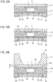
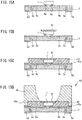
- FIGs 10C to 10E are cross-sectional views depicting production steps of the light emitting apparatus 20. Since the steps of mounting the LED device 1 on the circuit substrate 7 and bonding the phosphor layer 2 thereto are identical with Figures 7A and 7B , illustrations thereof are omitted.
- the diffusion plate 8 is placed thereafter on the upper surfaces of the phosphor layer 2 and the reflective resin 3 as depicted in Figure 10C . Then, the through-hole 8a of the diffusion plate 8 and the recessed portion 3a of the reflective resin 3 are formed at the same horizontal position as depicted in Figure 10D , for example, by cutting. Then, as depicted in Figure 10E , the protruded portion 9a of the reflection frame 9 is inserted into the recessed portion 3a of the reflective resin 3 through the through-hole 8a of the diffusion plate 8 to complete the light emitting apparatus 20.
- the operation of the light emitting apparatus 20 will be described.
- the LED device 1 when a drive voltage is applied to the power electrodes 5d, the LED device 1 emits light.
- blue light from the LED device 1 and yellow light generated by excitation of the phosphor layer 2 by the blue light are mixed to white light, which is then diffused by the diffusion plate 8.
- the light emitting apparatus 20 has a prevention effect against lateral light leakage similarly as the light emitting apparatus 10, and additionally against lateral light leakage from the diffusion plate 8 owing to the protruded portion 9a of the reflection frame 9.
- a diffusion plate 8 may be provided similarly as in the light emitting apparatus 20.
- Figures 11 and 12 are respectively a cross-sectional view and a top view of a light emitting apparatus 30.
- Figure 11 depicts a cross-section along the line XI-XI in Figure 12 .
- the basic constitution of the light emitting apparatus 30 is the same as the light emitting apparatus 10 depicted in Figures 1 and 2 . However, differently from the light emitting apparatus 10, the light emitting apparatus 30 has a lens 33 placed so as to cover an upper opening of the reflection frame 9.
- the lens 33 includes a round lens portion 33a (convex lens or concave lens) and a lens rim portion 33b surrounding the lens portion 33a.
- the lens 33 is fixed to the reflection frame 9 by fixing the lens rim portion 33b to the upper part of the reflection frame 9 with an adhesive or the like, in a state that the lens portion 33a is placed in the upper opening of the reflection frame 9.
- the operation of the light emitting apparatus 30 will be described.
- the LED device 1 when a drive voltage is applied to the power electrodes 5d, the LED device 1 emits light.
- blue light from the LED device 1 and yellow light generated by excitation of the phosphor layer 2 by the blue light are mixed to white light, which is then condensed by the reflection frame 9, and thereafter condensed again by the lens 33. Consequently, light well condensed and having excellent color rendering properties is emitted from the light emitting apparatus 30.
- a light emitting portion is configured with the phosphor layer 2 and the diffusion plate 8 in a platy form, and the injection-molded reflective resin 3 so as to prevent lateral light leakage. Further, the light emitting apparatus 10, 20 and 30 are assembled by fitting the protruded portion 9a into the recessed portion 3a, and this allows easy production. Moreover, since the reflection frame 9 is mounted engaging the protruded portion 9a with the recessed portion 3a in the light emitting apparatus 10, 20 and 30, the reflection frame can be interchanged according to need, when reflection frames having various shapes and characteristics have been prepared with a protruded portion with a common shape and position.
- Figures 13 and 14 are respectively a cross-sectional view and a top view of a light emitting apparatus 40.
- Figure 13 depicts a cross-section along the line XIII-XIII in Figure 14 .
- the light emitting apparatus 40 includes a circuit substrate 7.
- Wiring electrodes 5a and 5b are provided on the upper surface of the circuit substrate 7, and power electrodes 5d are provided on the back side of the circuit substrate 7.
- an LED device 1 is flip-chip mounted by electroconductive components 6a and 6b, and the wiring electrodes 5a and 5b are connected with the power electrodes 5d through through-hole electrodes 5c.
- a rectangular phosphor layer 42 having a size slightly larger than the light emitting surface of the LED device 1 is placed, and fixed to the LED device 1 by adhesion using a transparent adhesive, or the like.
- the side surface of the LED device 1 and the side surface of the phosphor layer 42 are sealed by filling a reflective resin 43, and a reflection frame 49 is mounted on the top of the reflective resin 43.
- a recessed step 43a and a protruded step 49a are respectively formed along the side circumference of the reflective resin 43, and along the side circumference of the reflection frame 49.
- the reflective resin 43 and the reflection frame 49 are fixed together by engaging the protruded step 49a with the recessed step 43a.
- the recessed step 43a and the protruded step 49a may be fixed together not only by simple engagement but also with a small amount of an adhesive.
- an entry aperture 49b through which light from the LED device 1 enters, is provided at the central position of the reflection frame 49, and the phosphor layer 42 is exposed in the entry aperture 49b.
- the reflection frame 49 is provided with a curved reflection surface 49d, which broadens from the entry aperture 49b toward an upward exit aperture 49c.
- the external shape of the phosphor layer 42 is also depicted by a dashed line, and the entry aperture 49b touches internally the rectangular phosphor layer 42. In other words, the upper surface of the phosphor layer 42 is larger than the entry aperture 49b of the reflection frame 49.
- Figures 15A to 15D are cross-sectional views depicting production steps of the light emitting apparatus 40.
- Figures 16A to 16D are top views depicting the production steps of the light emitting apparatus 40, and correspond respectively to Figures 15A to 15D .
- Figures 15A and 16A depict an LED mounting step, in which the LED device 1 is flip-chip mounted on the wiring electrodes 5a and 5b of the circuit substrate 7 by the electroconductive components 6a and 6b.
- Figures 15B and 16B depict a phosphor-layer bonding step, in which the phosphor layer 42 is fixed on the LED device 1 by applying a transparent adhesive to the upper surface of the LED device 1 and pressing the phosphor layer 42 thereon.
- Figures 15C and 16C depict a resin filling step, in which the side surface of the LED device 1 and the side surface of the phosphor layer 42 are sealed by filling the reflective resin 43 using an injection mold or the like. On this occasion, the recessed step 43a is formed along the side circumference of the reflective resin 43.
- Figures 15D and 16D depict a reflection-frame mounting step, in which the reflection frame 49 is fixed to the reflective resin 43 by engaging the protruded step 49a formed along the side circumference of the reflection frame 49 with the recessed step 43a formed along the side circumference of the reflective resin 43.
- the corners of the rectangular phosphor layer 42 are covered by the reflection frame 49, and the phosphor layer 42 is visible in a round form through the entry aperture 49b of the reflection frame 49.
- Figures 17 and 18 are respectively a cross-sectional view and a top view of a light emitting apparatus 50.
- Figure 17 depicts a cross-section along the line XVII-XVII in Figure 18 .
- the basic constitution of the light emitting apparatus 50 is the same as the light emitting apparatus 40 depicted in Figures 13 and 14 .
- the reflection frame 49 and the reflective resin 43 are fixed together by engaging the protruded step 49a with the recessed step 43a.
- the light emitting apparatus 50 has a round (disk-shaped) phosphor layer 52 placed on the light emitting surface of the LED device 1, and the shape and size of the upper surface of the phosphor layer 52 are identical with the shape and size of the entry aperture 49b of the reflection frame 49.
- Figures 19A to 19D are top views depicting production steps of the light emitting apparatus 50.
- the cross-sectional views depicting the production steps of the light emitting apparatus 50 are the same as the cross-sectional views in Figures 15A to 15D depicting the production steps of the light emitting apparatus 40.
- the round phosphor layer 52 is bonded to the upper surface of the LED device 1 in the phosphor bonding step depicted in Figure 19B . Since the shape and size of the phosphor layer 52 are nearly the same as those of the round entry aperture 49b of the reflection frame 49 as depicted in Figure 19D , the entire phosphor layer 52 is exposed.
- the entire phosphor layer 52 is exposed from the entry aperture 49b and the entire radiated light from the phosphor layer 52 can be utilized effectively. Consequently, the light emitting apparatus 50 can emit a larger amount of light.
- Figures 20 and 21 are respectively a cross-sectional view and a top view of a light emitting apparatus 60.
- Figure 20 depicts a cross-section along the line XX-XX in Figure 21 .
- the basic constitution of the light emitting apparatus 60 is the same as the light emitting apparatus 50 depicted in Figures 17 and 18 .
- a reflection frame 69 and the reflective resin 43 are fixed together by engaging a protruded step 69a formed along the side circumference of the reflection frame 69 with the recessed step 43a.
- the upper surface of a phosphor layer 62 and an entry aperture 69b of the reflection frame 69 of the light emitting apparatus 60 are both rectangular and reflection surfaces 69d curved and inclined in four directions are formed in the reflection frame 69, while in the light emitting apparatus 50 the upper surface of the phosphor layer 52 and the entry aperture 49b of the reflection frame 49 are both round. Further, the light emitting apparatus 60 has an exit aperture 69c which is also rectangular.
- Figures 22A to 22D are top views depicting production steps of the light emitting apparatus 60.
- the cross-sectional views depicting the production steps of the light emitting apparatus 60 are the same as the cross-sectional views in Figures 15A to 15D depicting the production steps of the light emitting apparatus 40.
- the rectangular phosphor layer 62 is bonded to the upper surface of the LED device 1 in the phosphor bonding step depicted in Figure 22B . Since the shape and size of the phosphor layer 62 is nearly the same as those of the rectangular entry aperture 69b of the reflection frame 69 as depicted in Figure 22D , the entire phosphor layer 62 is exposed.
- the entire phosphor layer 62 in a rectangular form is exposed from the entry aperture 69b and the entire radiated light from the phosphor layer 62 can be utilized effectively. Consequently, the light emitting apparatus 60 can further increase the amount of light.
- Figures 23 and 24 are respectively a cross-sectional view and a top view of a light emitting apparatus 70.
- Figure 23 depicts a cross-section along the line XXIII-XXIII in Figure 24 .
- the basic constitution of the light emitting apparatus 70 is the same as the light emitting apparatus 60 depicted in Figures 20 and 21 .
- a reflection frame 79 and the reflective resin 43 are fixed together by engaging a protruded step 79a formed along the side circumference of the reflection frame 79 with the recessed step 43a.
- the light emitting apparatus 70 has a rectangular phosphor layer 72 which is the same as the phosphor layer 62 of the light emitting apparatus 60.
- the reflection frame 79 of the light emitting apparatus 70 has a rectangular entry aperture 79b with rounded corners and curved and inclined reflection surfaces 79d in totally eight directions.
- the reflection surfaces 79d are constituted with reflection surfaces 79d1 corresponding to side surfaces in four directions, and reflection surfaces 79d2 corresponding to the corners in four directions.
- the corners of the phosphor layer 72 are slightly covered by the entry aperture 79b of the reflection frame 79.
- the amount of light can be increased and at the same time the condensing property of the emitted light can be enhanced.
- Figures 25A to 25D are top views depicting production steps of the light emitting apparatus 70.
- the cross-sectional views depicting the production steps of the light emitting apparatus 70 are the same as the cross-sectional views in Figures 15A to 15D depicting the production steps of the light emitting apparatus 40. Since the steps depicted in Figures 25A to 25C are the same as in the case of the light emitting apparatus 40, further descriptions will be omitted.
- Figures 26 and 27 are respectively a cross-sectional view and a top view of a light emitting apparatus 80.
- Figure 26 depicts a cross-section along the line XXVI-XXVI in Figure 27 .
- the basic constitution of the light emitting apparatus 80 is the same as the light emitting apparatus 50 depicted in Figures 17 and 18 .
- a reflection frame 89 and the reflective resin 43 are fixed together by engaging a protruded step 89a formed along the side circumference of the reflection frame 89 with the recessed step 43a.
- the light emitting apparatus 80 is provided with a lens 90 at a round exit aperture 89c provided at an upper part of the reflection frame 89.
- the lens 90 includes a central lens portion 90a and around the same a lens rim portion 90b.
- the lens portion 90a is a round convex lens, and the outer circumference of the lens rim portion 90b is rectangular.
- a mounting recessed portion 89e is formed around the exit aperture 89c of the reflection frame 89, and the lens rim portion 90b of the lens 90 is inserted into the mounting recessed portion 89e.
- the fitness of the round lens portion 90a can be enhanced. Further, by forming the mounting recessed portion 89e around the exit aperture 89c, the lens 90 can be easily mounted. Further, by collecting the light emitted from the LED device 1 and entered the entry aperture 89b with a reflection surface 89d of the reflection frame 89, and condensing the same by the lens 90, the condensing property of light can be enhanced.
- a light emitting portion free from lateral light leakage can be configured by sealing the side surfaces of the phosphor layers 42, 52, 62 and 72 and the LED device 1 with the reflective resin 43. Further, the light emitting apparatus 40 to 80 are assembled by fitting the recessed step 43a and the protruded steps 49a, 69a, 79a, and 89a formed respectively at the side circumferences of the reflective resin 43 and the reflection frames 49, 69, 79 and 89, and this allows easy production. Further, when reflection frames having various shapes and characteristics have been prepared with a protruded step of a common shape, and interchanged optionally, there can be a broad variety of functions and designs.
Landscapes
- Engineering & Computer Science (AREA)
- General Engineering & Computer Science (AREA)
- Physics & Mathematics (AREA)
- Microelectronics & Electronic Packaging (AREA)
- Optics & Photonics (AREA)
- Led Device Packages (AREA)
Claims (10)
- Appareil électroluminescent (20 ; 30 ; 40 ; 50 ; 60 ; 70 ; 80) comprenant :- un dispositif de diode électroluminescente (DEL) (1) sur un substrat (7),- une couche de phosphore (2 ; 42 ; 52 ; 62 ; 72) placée sur une surface électroluminescente du dispositif de DEL (1),- une résine réfléchissante (3 ; 43) couvrant la surface latérale du dispositif de DEL (1) et la surface latérale de la couche de phosphore (2 ; 42 ; 52 ; 62 ; 72), et- un cadre de réflexion (9 ; 49 ; 69 ; 79 ; 89) au-dessus de la couche de phosphore (2 ; 42 ; 52 ; 62 ; 72) et la résine réfléchissante (3 ; 43),
caractérisé en ce que- le dispositif de DEL (1) est une puce retournée (flip chip) montée sur le substrat (7),- la résine réfléchissante (3 ; 43) présente une partie évidée (3a) formée sur sa surface supérieure,- une couche de résine diffusante (8) est appliquée sur les surfaces supérieures de la couche de phosphore (2 ; 42 ; 52 ; 62 ; 72) et de la résine réfléchissante (3 ; 43), la couche de résine diffusante (8) présentant un trou traversant (8a) à une position correspondant à la partie évidée (3a) de la résine réfléchissante (3 ; 43),- le cadre de réflexion (9 ; 49 ; 69 ; 79 ; 89) présente une partie protubérante (9a) formée sur sa surface inférieure (9d), et- la partie protubérante (9a) du cadre de réflexion (9 ; 49 ; 69 ; 79 ; 89) passe par le trou traversant (8a) de la couche de résine diffusante (8) et engage avec la partie évidée (3a) de la résine réfléchissante (3 ; 43), et ce faisant le cadre de réflexion (9 ; 49 ; 69 ; 79 ; 89) est fixé au-dessus de la couche de phosphore (2 ; 42 ; 52 ; 62 ; 72) et la résine réfléchissante (3 ; 43) avec la couche de résine diffusante (8) interposée entre les deux. - Appareil électroluminescent (20 ; 30 ; 40 ; 50 ; 80) selon la revendication 1, dans lequel le cadre de réflexion (9 ; 49 ; 89) comprend une ouverture ronde prévue au-dessus de la couche de phosphore (2 ; 42 ; 52) et une surface de réflexion (9c ; 49d ; 89d) courbée prévue dans l'ouverture.
- Appareil électroluminescent (40 ; 50 ; 60 ; 70 ; 80) selon la revendication 1 ou 2, dans lequel- la résine réfléchissante (43) présente un épaulement évidé (43a) formé sur sa circonférence latéral en tant que partie évidée, et- le cadre de réflexion (49 ; 69 ; 79 ; 89) présente un épaulement protubérant (49a ; 69a ; 79a ; 89a) formé sur sa circonférence latéral en tant que partie protubérante.
- Appareil électroluminescent (40 ; 70) selon la revendication 3, dans lequel- le cadre de réflexion (49 ; 79) présente une fente d'entrée (49b ; 79b) dans laquelle lumière du dispositif de DEL (1) entre à travers la couche de phosphore (42 ; 72) et- la surface supérieure de la couche de phosphore (42 ; 72) est plus grande que la fente d'entrée (49b ; 79b) du cadre de réflexion (49 ; 79).
- Appareil électroluminescent (40) selon la revendication 4, dans lequel- la fente d'entrée (49b) du cadre de réflexion (49) est ronde et- la couche de phosphore (42) présente une surface supérieure rectangulaire et des coins couverts par le cadre de réflexion (49).
- Appareil électroluminescent (70) selon la revendication 4, dans lequel- la fente d'entrée (79b) du cadre de réflexion (79) est rectangulaire avec des coins ronds et- la couche de phosphore (72) présente une surface supérieure rectangulaire et des coins couverts par le cadre de réflexion (79).
- Appareil électroluminescent (50 ; 60 ; 80) selon la revendication 3, dans lequel- le cadre de réflexion (49 ; 69 ; 89) présente une fente d'entrée (49b ; 69b ; 89b) dans laquelle lumière du dispositif de DEL (1) entre à travers la couche de phosphore (52 ; 62) et- la couche de phosphore (52 ; 62) présente une surface supérieure dont la forme et taille sont presque identiques à la forme et taille de la fente d'entrée (49b ; 69b ; 89b) du cadre de réflexion (49 ; 69 ; 89).
- Appareil électroluminescent (50 ; 80) selon la revendication 7, dans lequel la surface supérieure de la couche de phosphore (52) et la fente d'entrée (49b ; 89b) du cadre de réflexion (49 ; 89) sont ronds tous deux.
- Appareil électroluminescent (60) selon la revendication 7, dans lequel la surface supérieure de la couche de phosphore (62) et la fente d'entrée (69b) du cadre de réflexion (69) sont rectangulaires tous deux.
- Appareil électroluminescent (30 ; 80) selon la revendication 1, dans lequel- le cadre de réflexion (9 ; 89) présente une fente d'entrée (9b ; 89b) dans laquelle lumière du dispositif de DEL (1) entre à travers la couche de phosphore (2 ; 52) et une fente de sortie (89c) à une position opposée à la fente d'entrée (9b ; 89b) et- l'appareil électroluminescent (30 ; 80) comprend en outre une lentille (33 ; 90) placée pour couvrir la fente de sortie (89c) du cadre de réflexion (9 ; 89).
Priority Applications (1)
| Application Number | Priority Date | Filing Date | Title |
|---|---|---|---|
| EP19175324.3A EP3547379A1 (fr) | 2014-03-14 | 2015-03-05 | Appareil électroluminescent |
Applications Claiming Priority (2)
| Application Number | Priority Date | Filing Date | Title |
|---|---|---|---|
| JP2014051040A JP6216272B2 (ja) | 2014-03-14 | 2014-03-14 | Led発光装置 |
| JP2014052117A JP6259329B2 (ja) | 2014-03-14 | 2014-03-14 | Led発光装置 |
Related Child Applications (2)
| Application Number | Title | Priority Date | Filing Date |
|---|---|---|---|
| EP19175324.3A Division-Into EP3547379A1 (fr) | 2014-03-14 | 2015-03-05 | Appareil électroluminescent |
| EP19175324.3A Division EP3547379A1 (fr) | 2014-03-14 | 2015-03-05 | Appareil électroluminescent |
Publications (2)
| Publication Number | Publication Date |
|---|---|
| EP2919284A1 EP2919284A1 (fr) | 2015-09-16 |
| EP2919284B1 true EP2919284B1 (fr) | 2019-07-03 |
Family
ID=52598655
Family Applications (2)
| Application Number | Title | Priority Date | Filing Date |
|---|---|---|---|
| EP15157736.8A Active EP2919284B1 (fr) | 2014-03-14 | 2015-03-05 | Appareil électroluminescent |
| EP19175324.3A Withdrawn EP3547379A1 (fr) | 2014-03-14 | 2015-03-05 | Appareil électroluminescent |
Family Applications After (1)
| Application Number | Title | Priority Date | Filing Date |
|---|---|---|---|
| EP19175324.3A Withdrawn EP3547379A1 (fr) | 2014-03-14 | 2015-03-05 | Appareil électroluminescent |
Country Status (3)
| Country | Link |
|---|---|
| US (1) | US9728684B2 (fr) |
| EP (2) | EP2919284B1 (fr) |
| CN (1) | CN104916759B (fr) |
Families Citing this family (35)
| Publication number | Priority date | Publication date | Assignee | Title |
|---|---|---|---|---|
| US9587803B1 (en) * | 2013-08-23 | 2017-03-07 | Cooper Technologies Company | High voltage lighting fixture |
| USD875284S1 (en) | 2015-10-16 | 2020-02-11 | Walter R. Tucker Enterprises, Ltd. | Portable light |
| USD863632S1 (en) | 2015-10-16 | 2019-10-15 | Walter R. Tucker Enterprises, Ltd. | Portable light lens |
| US9951930B2 (en) | 2015-10-16 | 2018-04-24 | Walter R. Tucker Enterprises, Ltd. | Portable light |
| USD866027S1 (en) | 2015-10-16 | 2019-11-05 | Walter R. Tucker Enterprises, Ltd. | Portable light |
| CN106601898A (zh) * | 2015-10-19 | 2017-04-26 | 展晶科技(深圳)有限公司 | 发光二极管封装结构 |
| KR102432222B1 (ko) * | 2015-11-04 | 2022-08-17 | 쑤저우 레킨 세미컨덕터 컴퍼니 리미티드 | 광학 플레이트, 조명 소자 및 광원 모듈 |
| KR102432219B1 (ko) * | 2015-11-04 | 2022-08-17 | 쑤저우 레킨 세미컨덕터 컴퍼니 리미티드 | 광학 플레이트, 조명 소자 및 광원 모듈 |
| KR102450123B1 (ko) * | 2015-11-04 | 2022-10-04 | 쑤저우 레킨 세미컨덕터 컴퍼니 리미티드 | 광학 플레이트, 조명 소자 및 광원 모듈 |
| JP2017135253A (ja) * | 2016-01-27 | 2017-08-03 | オムロン株式会社 | 発光装置、および発光装置の製造方法 |
| DE102016108692A1 (de) * | 2016-05-11 | 2017-11-16 | Osram Gmbh | Leuchtdiode und Leuchtmodul |
| CN107403791B (zh) * | 2016-05-18 | 2020-04-10 | 光宝光电(常州)有限公司 | 发光显示器以及形成发光显示器的方法 |
| CN107482099B (zh) * | 2016-06-08 | 2019-09-10 | 光宝光电(常州)有限公司 | 发光二极管封装结构 |
| TWI626771B (zh) * | 2016-07-26 | 2018-06-11 | 宏齊科技股份有限公司 | 發光二極體單元和薄型平面光源模組 |
| CN106210473B (zh) * | 2016-08-10 | 2019-09-20 | 青岛海信移动通信技术股份有限公司 | 终端设备 |
| JP6455495B2 (ja) * | 2016-09-28 | 2019-01-23 | 日亜化学工業株式会社 | 発光装置及びその製造方法 |
| USD829354S1 (en) | 2016-12-22 | 2018-09-25 | Walter R. Tucker Enterprises, Ltd. | Portable light |
| CN108269898B (zh) * | 2016-12-30 | 2019-10-18 | 光宝光电(常州)有限公司 | 发光二极管封装结构 |
| CN108269899B (zh) * | 2016-12-30 | 2020-06-05 | 光宝光电(常州)有限公司 | 发光二极管封装结构及其制造方法 |
| JP6662322B2 (ja) | 2017-02-09 | 2020-03-11 | 日亜化学工業株式会社 | 発光装置 |
| JP1611148S (fr) * | 2017-12-07 | 2018-08-13 | ||
| JP7015686B2 (ja) * | 2017-12-14 | 2022-02-03 | 旭化成エレクトロニクス株式会社 | 光デバイス及び光デバイスの製造方法 |
| EP3757629B1 (fr) * | 2018-02-19 | 2024-03-06 | NGK Insulators, Ltd. | Composant optique et dispositif d'éclairage |
| JP7054005B2 (ja) | 2018-09-28 | 2022-04-13 | 日亜化学工業株式会社 | 発光装置 |
| JP7282620B2 (ja) * | 2019-07-04 | 2023-05-29 | シャープ福山レーザー株式会社 | 画像表示素子 |
| CN112216774A (zh) * | 2019-07-11 | 2021-01-12 | 成都辰显光电有限公司 | 色彩转换组件、显示面板及制作方法 |
| JP7105415B2 (ja) * | 2020-02-20 | 2022-07-25 | 日亜化学工業株式会社 | 発光装置及びその製造方法 |
| TWI871304B (zh) * | 2020-03-02 | 2025-02-01 | 晶智達光電股份有限公司 | 雷射封裝結構 |
| TWI887269B (zh) * | 2020-09-17 | 2025-06-21 | 晶智達光電股份有限公司 | 雷射封裝結構 |
| WO2022131885A1 (fr) * | 2020-12-18 | 2022-06-23 | 서울바이오시스주식회사 | Boîtier de diode électroluminescente |
| DE102021110089A1 (de) * | 2021-04-21 | 2022-10-27 | OSRAM Opto Semiconductors Gesellschaft mit beschränkter Haftung | Verfahren zur herstellung eines bauteils mit kavität und bauteil mit kavität |
| KR20230034562A (ko) * | 2021-09-03 | 2023-03-10 | 현대자동차주식회사 | 색변환 물질을 활용한 히든 라이팅 램프 및 차량 |
| DE102021131112A1 (de) * | 2021-11-26 | 2023-06-01 | OSRAM Opto Semiconductors Gesellschaft mit beschränkter Haftung | Strahlungsemittierendes bauelement und verfahren zur herstellung eines strahlungsemittierenden bauelements |
| WO2023227324A1 (fr) * | 2022-05-24 | 2023-11-30 | Ams-Osram International Gmbh | Dispositif optoélectronique et procédé de production de dispositif optoélectronique |
| US20240055570A1 (en) * | 2022-08-11 | 2024-02-15 | Creeled, Inc. | Light emitting device with light-altering material layer, and fabrication method utilizing sealing template |
Family Cites Families (13)
| Publication number | Priority date | Publication date | Assignee | Title |
|---|---|---|---|---|
| US6274890B1 (en) * | 1997-01-15 | 2001-08-14 | Kabushiki Kaisha Toshiba | Semiconductor light emitting device and its manufacturing method |
| JP3798195B2 (ja) * | 1999-08-12 | 2006-07-19 | ローム株式会社 | チップ型発光装置 |
| JP4504662B2 (ja) * | 2003-04-09 | 2010-07-14 | シチズン電子株式会社 | Ledランプ |
| DE102004045950A1 (de) * | 2004-09-22 | 2006-03-30 | Osram Opto Semiconductors Gmbh | Gehäuse für ein optoelektronisches Bauelement, optoelektronisches Bauelement und Verfahren zur Herstellung eines optoelektronischen Bauelements |
| DE112006000694B4 (de) * | 2005-03-24 | 2013-10-17 | Kyocera Corp. | Gehäuse für Lichtemissionsvorrichtung, lichtemittierende Vorrichtung und Beleuchtungsvorrichtung |
| JP5482378B2 (ja) * | 2009-04-20 | 2014-05-07 | 日亜化学工業株式会社 | 発光装置 |
| US8097894B2 (en) * | 2009-07-23 | 2012-01-17 | Koninklijke Philips Electronics N.V. | LED with molded reflective sidewall coating |
| JP5350947B2 (ja) | 2009-09-04 | 2013-11-27 | シャープ株式会社 | 発光ダイオード |
| DE102010027253B4 (de) * | 2010-07-15 | 2022-05-12 | OSRAM Opto Semiconductors Gesellschaft mit beschränkter Haftung | Optoelektronisches Halbleiterbauteil |
| DE102010045403A1 (de) * | 2010-09-15 | 2012-03-15 | Osram Opto Semiconductors Gmbh | Optoelektronisches Bauelement |
| CN108565329A (zh) * | 2011-11-17 | 2018-09-21 | 株式会社流明斯 | 发光元件封装体以及包括该发光元件封装体的背光单元 |
| KR101973395B1 (ko) * | 2012-08-09 | 2019-04-29 | 엘지이노텍 주식회사 | 발광 모듈 |
| JP5374002B1 (ja) * | 2012-09-10 | 2013-12-25 | パナソニック株式会社 | 窒化物半導体発光装置 |
-
2015
- 2015-03-05 EP EP15157736.8A patent/EP2919284B1/fr active Active
- 2015-03-05 EP EP19175324.3A patent/EP3547379A1/fr not_active Withdrawn
- 2015-03-11 US US14/645,002 patent/US9728684B2/en active Active
- 2015-03-12 CN CN201510109223.6A patent/CN104916759B/zh active Active
Non-Patent Citations (1)
| Title |
|---|
| None * |
Also Published As
| Publication number | Publication date |
|---|---|
| CN104916759A (zh) | 2015-09-16 |
| US20150263239A1 (en) | 2015-09-17 |
| CN104916759B (zh) | 2018-12-21 |
| US9728684B2 (en) | 2017-08-08 |
| EP2919284A1 (fr) | 2015-09-16 |
| EP3547379A1 (fr) | 2019-10-02 |
Similar Documents
| Publication | Publication Date | Title |
|---|---|---|
| EP2919284B1 (fr) | Appareil électroluminescent | |
| US8039862B2 (en) | White light emitting diode package having enhanced white lighting efficiency and method of making the same | |
| US20110062470A1 (en) | Reduced angular emission cone illumination leds | |
| JP4046118B2 (ja) | 発光素子、それを用いた発光装置及び面発光照明装置 | |
| KR101064036B1 (ko) | 발광 소자 패키지 및 조명 시스템 | |
| KR20060049072A (ko) | 발광 다이오드 램프 | |
| JP6221403B2 (ja) | 発光装置 | |
| CN102347421A (zh) | 发光装置 | |
| JP2004281605A (ja) | Ledパッケージ | |
| WO2007114306A1 (fr) | Dispositif electroluminescent | |
| JP2019212739A (ja) | 発光装置および面発光光源 | |
| JP6216272B2 (ja) | Led発光装置 | |
| US10825971B2 (en) | Light-emitting device including a Distributed Bragg Reflector (DBR) film | |
| KR20140095913A (ko) | 발광 모듈 및 이를 구비한 조명 장치 | |
| JP6189661B2 (ja) | 半導体発光装置 | |
| KR101220038B1 (ko) | 발광 장치 | |
| KR102432222B1 (ko) | 광학 플레이트, 조명 소자 및 광원 모듈 | |
| JP4246215B2 (ja) | 光源装置および平面照明装置 | |
| JP2016028461A (ja) | Led発光装置 | |
| KR20170052204A (ko) | 광학 플레이트, 조명 소자 및 광원 모듈 | |
| KR102024297B1 (ko) | 렌즈모듈 및 이를 포함하는 발광소자패키지 | |
| US20140175479A1 (en) | Led unit with light mixing element | |
| KR20220137587A (ko) | 광학 플레이트, 조명 소자 및 광원 모듈 | |
| KR20170052207A (ko) | 광학 플레이트, 발광 소자 및 광원 모듈 | |
| KR101778151B1 (ko) | 발광소자 패키지 |
Legal Events
| Date | Code | Title | Description |
|---|---|---|---|
| PUAI | Public reference made under article 153(3) epc to a published international application that has entered the european phase |
Free format text: ORIGINAL CODE: 0009012 |
|
| AK | Designated contracting states |
Kind code of ref document: A1 Designated state(s): AL AT BE BG CH CY CZ DE DK EE ES FI FR GB GR HR HU IE IS IT LI LT LU LV MC MK MT NL NO PL PT RO RS SE SI SK SM TR |
|
| AX | Request for extension of the european patent |
Extension state: BA ME |
|
| 17P | Request for examination filed |
Effective date: 20160129 |
|
| RBV | Designated contracting states (corrected) |
Designated state(s): AL AT BE BG CH CY CZ DE DK EE ES FI FR GB GR HR HU IE IS IT LI LT LU LV MC MK MT NL NO PL PT RO RS SE SI SK SM TR |
|
| RAP1 | Party data changed (applicant data changed or rights of an application transferred) |
Owner name: CITIZEN WATCH CO., LTD. Owner name: CITIZEN ELECTRONICS CO., LTD. |
|
| REG | Reference to a national code |
Ref country code: DE Ref legal event code: R079 Ref document number: 602015032971 Country of ref document: DE Free format text: PREVIOUS MAIN CLASS: H01L0033500000 Ipc: H01L0033540000 |
|
| RIC1 | Information provided on ipc code assigned before grant |
Ipc: F21Y 115/10 20160101ALN20181122BHEP Ipc: H01L 33/60 20100101ALN20181122BHEP Ipc: H01L 33/50 20100101ALN20181122BHEP Ipc: H01L 33/54 20100101AFI20181122BHEP |
|
| GRAP | Despatch of communication of intention to grant a patent |
Free format text: ORIGINAL CODE: EPIDOSNIGR1 |
|
| RIC1 | Information provided on ipc code assigned before grant |
Ipc: H01L 33/60 20100101ALN20181205BHEP Ipc: F21Y 115/10 20160101ALN20181205BHEP Ipc: H01L 33/50 20100101ALN20181205BHEP Ipc: H01L 33/54 20100101AFI20181205BHEP |
|
| STAA | Information on the status of an ep patent application or granted ep patent |
Free format text: STATUS: GRANT OF PATENT IS INTENDED |
|
| INTG | Intention to grant announced |
Effective date: 20190110 |
|
| RIC1 | Information provided on ipc code assigned before grant |
Ipc: F21Y 115/10 20160101ALN20181205BHEP Ipc: H01L 33/54 20100101AFI20181205BHEP Ipc: H01L 33/50 20100101ALN20181205BHEP Ipc: H01L 33/60 20100101ALN20181205BHEP |
|
| GRAS | Grant fee paid |
Free format text: ORIGINAL CODE: EPIDOSNIGR3 |
|
| GRAA | (expected) grant |
Free format text: ORIGINAL CODE: 0009210 |
|
| STAA | Information on the status of an ep patent application or granted ep patent |
Free format text: STATUS: THE PATENT HAS BEEN GRANTED |
|
| AK | Designated contracting states |
Kind code of ref document: B1 Designated state(s): AL AT BE BG CH CY CZ DE DK EE ES FI FR GB GR HR HU IE IS IT LI LT LU LV MC MK MT NL NO PL PT RO RS SE SI SK SM TR |
|
| REG | Reference to a national code |
Ref country code: GB Ref legal event code: FG4D |
|
| REG | Reference to a national code |
Ref country code: CH Ref legal event code: EP Ref country code: AT Ref legal event code: REF Ref document number: 1152031 Country of ref document: AT Kind code of ref document: T Effective date: 20190715 |
|
| REG | Reference to a national code |
Ref country code: IE Ref legal event code: FG4D |
|
| REG | Reference to a national code |
Ref country code: DE Ref legal event code: R096 Ref document number: 602015032971 Country of ref document: DE |
|
| REG | Reference to a national code |
Ref country code: NL Ref legal event code: MP Effective date: 20190703 |
|
| REG | Reference to a national code |
Ref country code: LT Ref legal event code: MG4D |
|
| REG | Reference to a national code |
Ref country code: AT Ref legal event code: MK05 Ref document number: 1152031 Country of ref document: AT Kind code of ref document: T Effective date: 20190703 |
|
| PG25 | Lapsed in a contracting state [announced via postgrant information from national office to epo] |
Ref country code: PT Free format text: LAPSE BECAUSE OF FAILURE TO SUBMIT A TRANSLATION OF THE DESCRIPTION OR TO PAY THE FEE WITHIN THE PRESCRIBED TIME-LIMIT Effective date: 20191104 Ref country code: HR Free format text: LAPSE BECAUSE OF FAILURE TO SUBMIT A TRANSLATION OF THE DESCRIPTION OR TO PAY THE FEE WITHIN THE PRESCRIBED TIME-LIMIT Effective date: 20190703 Ref country code: AT Free format text: LAPSE BECAUSE OF FAILURE TO SUBMIT A TRANSLATION OF THE DESCRIPTION OR TO PAY THE FEE WITHIN THE PRESCRIBED TIME-LIMIT Effective date: 20190703 Ref country code: BG Free format text: LAPSE BECAUSE OF FAILURE TO SUBMIT A TRANSLATION OF THE DESCRIPTION OR TO PAY THE FEE WITHIN THE PRESCRIBED TIME-LIMIT Effective date: 20191003 Ref country code: NL Free format text: LAPSE BECAUSE OF FAILURE TO SUBMIT A TRANSLATION OF THE DESCRIPTION OR TO PAY THE FEE WITHIN THE PRESCRIBED TIME-LIMIT Effective date: 20190703 Ref country code: LT Free format text: LAPSE BECAUSE OF FAILURE TO SUBMIT A TRANSLATION OF THE DESCRIPTION OR TO PAY THE FEE WITHIN THE PRESCRIBED TIME-LIMIT Effective date: 20190703 Ref country code: CZ Free format text: LAPSE BECAUSE OF FAILURE TO SUBMIT A TRANSLATION OF THE DESCRIPTION OR TO PAY THE FEE WITHIN THE PRESCRIBED TIME-LIMIT Effective date: 20190703 Ref country code: FI Free format text: LAPSE BECAUSE OF FAILURE TO SUBMIT A TRANSLATION OF THE DESCRIPTION OR TO PAY THE FEE WITHIN THE PRESCRIBED TIME-LIMIT Effective date: 20190703 Ref country code: NO Free format text: LAPSE BECAUSE OF FAILURE TO SUBMIT A TRANSLATION OF THE DESCRIPTION OR TO PAY THE FEE WITHIN THE PRESCRIBED TIME-LIMIT Effective date: 20191003 Ref country code: SE Free format text: LAPSE BECAUSE OF FAILURE TO SUBMIT A TRANSLATION OF THE DESCRIPTION OR TO PAY THE FEE WITHIN THE PRESCRIBED TIME-LIMIT Effective date: 20190703 |
|
| PG25 | Lapsed in a contracting state [announced via postgrant information from national office to epo] |
Ref country code: IS Free format text: LAPSE BECAUSE OF FAILURE TO SUBMIT A TRANSLATION OF THE DESCRIPTION OR TO PAY THE FEE WITHIN THE PRESCRIBED TIME-LIMIT Effective date: 20191103 Ref country code: GR Free format text: LAPSE BECAUSE OF FAILURE TO SUBMIT A TRANSLATION OF THE DESCRIPTION OR TO PAY THE FEE WITHIN THE PRESCRIBED TIME-LIMIT Effective date: 20191004 Ref country code: RS Free format text: LAPSE BECAUSE OF FAILURE TO SUBMIT A TRANSLATION OF THE DESCRIPTION OR TO PAY THE FEE WITHIN THE PRESCRIBED TIME-LIMIT Effective date: 20190703 Ref country code: ES Free format text: LAPSE BECAUSE OF FAILURE TO SUBMIT A TRANSLATION OF THE DESCRIPTION OR TO PAY THE FEE WITHIN THE PRESCRIBED TIME-LIMIT Effective date: 20190703 Ref country code: AL Free format text: LAPSE BECAUSE OF FAILURE TO SUBMIT A TRANSLATION OF THE DESCRIPTION OR TO PAY THE FEE WITHIN THE PRESCRIBED TIME-LIMIT Effective date: 20190703 Ref country code: LV Free format text: LAPSE BECAUSE OF FAILURE TO SUBMIT A TRANSLATION OF THE DESCRIPTION OR TO PAY THE FEE WITHIN THE PRESCRIBED TIME-LIMIT Effective date: 20190703 |
|
| PG25 | Lapsed in a contracting state [announced via postgrant information from national office to epo] |
Ref country code: TR Free format text: LAPSE BECAUSE OF FAILURE TO SUBMIT A TRANSLATION OF THE DESCRIPTION OR TO PAY THE FEE WITHIN THE PRESCRIBED TIME-LIMIT Effective date: 20190703 |
|
| PG25 | Lapsed in a contracting state [announced via postgrant information from national office to epo] |
Ref country code: EE Free format text: LAPSE BECAUSE OF FAILURE TO SUBMIT A TRANSLATION OF THE DESCRIPTION OR TO PAY THE FEE WITHIN THE PRESCRIBED TIME-LIMIT Effective date: 20190703 Ref country code: DK Free format text: LAPSE BECAUSE OF FAILURE TO SUBMIT A TRANSLATION OF THE DESCRIPTION OR TO PAY THE FEE WITHIN THE PRESCRIBED TIME-LIMIT Effective date: 20190703 Ref country code: IT Free format text: LAPSE BECAUSE OF FAILURE TO SUBMIT A TRANSLATION OF THE DESCRIPTION OR TO PAY THE FEE WITHIN THE PRESCRIBED TIME-LIMIT Effective date: 20190703 Ref country code: RO Free format text: LAPSE BECAUSE OF FAILURE TO SUBMIT A TRANSLATION OF THE DESCRIPTION OR TO PAY THE FEE WITHIN THE PRESCRIBED TIME-LIMIT Effective date: 20190703 Ref country code: PL Free format text: LAPSE BECAUSE OF FAILURE TO SUBMIT A TRANSLATION OF THE DESCRIPTION OR TO PAY THE FEE WITHIN THE PRESCRIBED TIME-LIMIT Effective date: 20190703 |
|
| PG25 | Lapsed in a contracting state [announced via postgrant information from national office to epo] |
Ref country code: SK Free format text: LAPSE BECAUSE OF FAILURE TO SUBMIT A TRANSLATION OF THE DESCRIPTION OR TO PAY THE FEE WITHIN THE PRESCRIBED TIME-LIMIT Effective date: 20190703 Ref country code: SM Free format text: LAPSE BECAUSE OF FAILURE TO SUBMIT A TRANSLATION OF THE DESCRIPTION OR TO PAY THE FEE WITHIN THE PRESCRIBED TIME-LIMIT Effective date: 20190703 Ref country code: IS Free format text: LAPSE BECAUSE OF FAILURE TO SUBMIT A TRANSLATION OF THE DESCRIPTION OR TO PAY THE FEE WITHIN THE PRESCRIBED TIME-LIMIT Effective date: 20200224 |
|
| REG | Reference to a national code |
Ref country code: DE Ref legal event code: R097 Ref document number: 602015032971 Country of ref document: DE |
|
| PLBE | No opposition filed within time limit |
Free format text: ORIGINAL CODE: 0009261 |
|
| STAA | Information on the status of an ep patent application or granted ep patent |
Free format text: STATUS: NO OPPOSITION FILED WITHIN TIME LIMIT |
|
| PG2D | Information on lapse in contracting state deleted |
Ref country code: IS |
|
| 26N | No opposition filed |
Effective date: 20200603 |
|
| PG25 | Lapsed in a contracting state [announced via postgrant information from national office to epo] |
Ref country code: SI Free format text: LAPSE BECAUSE OF FAILURE TO SUBMIT A TRANSLATION OF THE DESCRIPTION OR TO PAY THE FEE WITHIN THE PRESCRIBED TIME-LIMIT Effective date: 20190703 |
|
| PG25 | Lapsed in a contracting state [announced via postgrant information from national office to epo] |
Ref country code: MC Free format text: LAPSE BECAUSE OF FAILURE TO SUBMIT A TRANSLATION OF THE DESCRIPTION OR TO PAY THE FEE WITHIN THE PRESCRIBED TIME-LIMIT Effective date: 20190703 |
|
| REG | Reference to a national code |
Ref country code: CH Ref legal event code: PL |
|
| REG | Reference to a national code |
Ref country code: BE Ref legal event code: MM Effective date: 20200331 |
|
| PG25 | Lapsed in a contracting state [announced via postgrant information from national office to epo] |
Ref country code: LU Free format text: LAPSE BECAUSE OF NON-PAYMENT OF DUE FEES Effective date: 20200305 |
|
| PG25 | Lapsed in a contracting state [announced via postgrant information from national office to epo] |
Ref country code: FR Free format text: LAPSE BECAUSE OF NON-PAYMENT OF DUE FEES Effective date: 20200331 Ref country code: CH Free format text: LAPSE BECAUSE OF NON-PAYMENT OF DUE FEES Effective date: 20200331 Ref country code: IE Free format text: LAPSE BECAUSE OF NON-PAYMENT OF DUE FEES Effective date: 20200305 Ref country code: LI Free format text: LAPSE BECAUSE OF NON-PAYMENT OF DUE FEES Effective date: 20200331 |
|
| PG25 | Lapsed in a contracting state [announced via postgrant information from national office to epo] |
Ref country code: BE Free format text: LAPSE BECAUSE OF NON-PAYMENT OF DUE FEES Effective date: 20200331 |
|
| GBPC | Gb: european patent ceased through non-payment of renewal fee |
Effective date: 20200305 |
|
| PG25 | Lapsed in a contracting state [announced via postgrant information from national office to epo] |
Ref country code: GB Free format text: LAPSE BECAUSE OF NON-PAYMENT OF DUE FEES Effective date: 20200305 |
|
| PG25 | Lapsed in a contracting state [announced via postgrant information from national office to epo] |
Ref country code: MT Free format text: LAPSE BECAUSE OF FAILURE TO SUBMIT A TRANSLATION OF THE DESCRIPTION OR TO PAY THE FEE WITHIN THE PRESCRIBED TIME-LIMIT Effective date: 20190703 Ref country code: CY Free format text: LAPSE BECAUSE OF FAILURE TO SUBMIT A TRANSLATION OF THE DESCRIPTION OR TO PAY THE FEE WITHIN THE PRESCRIBED TIME-LIMIT Effective date: 20190703 |
|
| PG25 | Lapsed in a contracting state [announced via postgrant information from national office to epo] |
Ref country code: MK Free format text: LAPSE BECAUSE OF FAILURE TO SUBMIT A TRANSLATION OF THE DESCRIPTION OR TO PAY THE FEE WITHIN THE PRESCRIBED TIME-LIMIT Effective date: 20190703 |
|
| REG | Reference to a national code |
Ref country code: DE Ref legal event code: R079 Ref document number: 602015032971 Country of ref document: DE Free format text: PREVIOUS MAIN CLASS: H01L0033540000 Ipc: H10H0020853000 |
|
| PGFP | Annual fee paid to national office [announced via postgrant information from national office to epo] |
Ref country code: DE Payment date: 20250128 Year of fee payment: 11 |