EP2919326B1 - Connecteur et procédé d'assemblage pour ensemble de transmission de connecteur - Google Patents
Connecteur et procédé d'assemblage pour ensemble de transmission de connecteur Download PDFInfo
- Publication number
- EP2919326B1 EP2919326B1 EP14158703.0A EP14158703A EP2919326B1 EP 2919326 B1 EP2919326 B1 EP 2919326B1 EP 14158703 A EP14158703 A EP 14158703A EP 2919326 B1 EP2919326 B1 EP 2919326B1
- Authority
- EP
- European Patent Office
- Prior art keywords
- circuit board
- terminals
- terminal
- connector
- lateral side
- Prior art date
- Legal status (The legal status is an assumption and is not a legal conclusion. Google has not performed a legal analysis and makes no representation as to the accuracy of the status listed.)
- Active
Links
Images




Classifications
-
- H—ELECTRICITY
- H01—ELECTRIC ELEMENTS
- H01R—ELECTRICALLY-CONDUCTIVE CONNECTIONS; STRUCTURAL ASSOCIATIONS OF A PLURALITY OF MUTUALLY-INSULATED ELECTRICAL CONNECTING ELEMENTS; COUPLING DEVICES; CURRENT COLLECTORS
- H01R24/00—Two-part coupling devices, or either of their cooperating parts, characterised by their overall structure
- H01R24/60—Contacts spaced along planar side wall transverse to longitudinal axis of engagement
- H01R24/62—Sliding engagements with one side only, e.g. modular jack coupling devices
- H01R24/64—Sliding engagements with one side only, e.g. modular jack coupling devices for high frequency, e.g. RJ 45
-
- H—ELECTRICITY
- H01—ELECTRIC ELEMENTS
- H01R—ELECTRICALLY-CONDUCTIVE CONNECTIONS; STRUCTURAL ASSOCIATIONS OF A PLURALITY OF MUTUALLY-INSULATED ELECTRICAL CONNECTING ELEMENTS; COUPLING DEVICES; CURRENT COLLECTORS
- H01R12/00—Structural associations of a plurality of mutually-insulated electrical connecting elements, specially adapted for printed circuits, e.g. printed circuit boards [PCB], flat or ribbon cables, or like generally planar structures, e.g. terminal strips, terminal blocks; Coupling devices specially adapted for printed circuits, flat or ribbon cables, or like generally planar structures; Terminals specially adapted for contact with, or insertion into, printed circuits, flat or ribbon cables, or like generally planar structures
- H01R12/50—Fixed connections
- H01R12/51—Fixed connections for rigid printed circuits or like structures
- H01R12/52—Fixed connections for rigid printed circuits or like structures connecting to other rigid printed circuits or like structures
-
- H—ELECTRICITY
- H01—ELECTRIC ELEMENTS
- H01R—ELECTRICALLY-CONDUCTIVE CONNECTIONS; STRUCTURAL ASSOCIATIONS OF A PLURALITY OF MUTUALLY-INSULATED ELECTRICAL CONNECTING ELEMENTS; COUPLING DEVICES; CURRENT COLLECTORS
- H01R13/00—Details of coupling devices of the kinds covered by groups H01R12/70 or H01R24/00 - H01R33/00
- H01R13/646—Details of coupling devices of the kinds covered by groups H01R12/70 or H01R24/00 - H01R33/00 specially adapted for high-frequency, e.g. structures providing an impedance match or phase match
- H01R13/6461—Means for preventing cross-talk
- H01R13/6467—Means for preventing cross-talk by cross-over of signal conductors
-
- H—ELECTRICITY
- H05—ELECTRIC TECHNIQUES NOT OTHERWISE PROVIDED FOR
- H05K—PRINTED CIRCUITS; CASINGS OR CONSTRUCTIONAL DETAILS OF ELECTRIC APPARATUS; MANUFACTURE OF ASSEMBLAGES OF ELECTRICAL COMPONENTS
- H05K1/00—Printed circuits
- H05K1/02—Details
- H05K1/14—Structural association of two or more printed circuits
- H05K1/144—Stacked arrangements of planar printed circuit boards
-
- H—ELECTRICITY
- H05—ELECTRIC TECHNIQUES NOT OTHERWISE PROVIDED FOR
- H05K—PRINTED CIRCUITS; CASINGS OR CONSTRUCTIONAL DETAILS OF ELECTRIC APPARATUS; MANUFACTURE OF ASSEMBLAGES OF ELECTRICAL COMPONENTS
- H05K3/00—Apparatus or processes for manufacturing printed circuits
- H05K3/36—Assembling printed circuits with other printed circuits
- H05K3/368—Assembling printed circuits with other printed circuits parallel to each other
-
- H—ELECTRICITY
- H05—ELECTRIC TECHNIQUES NOT OTHERWISE PROVIDED FOR
- H05K—PRINTED CIRCUITS; CASINGS OR CONSTRUCTIONAL DETAILS OF ELECTRIC APPARATUS; MANUFACTURE OF ASSEMBLAGES OF ELECTRICAL COMPONENTS
- H05K3/00—Apparatus or processes for manufacturing printed circuits
- H05K3/40—Forming printed elements for providing electric connections to or between printed circuits
- H05K3/403—Edge contacts; Windows or holes in the substrate having plural connections on the walls thereof
-
- H—ELECTRICITY
- H01—ELECTRIC ELEMENTS
- H01R—ELECTRICALLY-CONDUCTIVE CONNECTIONS; STRUCTURAL ASSOCIATIONS OF A PLURALITY OF MUTUALLY-INSULATED ELECTRICAL CONNECTING ELEMENTS; COUPLING DEVICES; CURRENT COLLECTORS
- H01R13/00—Details of coupling devices of the kinds covered by groups H01R12/70 or H01R24/00 - H01R33/00
- H01R13/646—Details of coupling devices of the kinds covered by groups H01R12/70 or H01R24/00 - H01R33/00 specially adapted for high-frequency, e.g. structures providing an impedance match or phase match
- H01R13/6461—Means for preventing cross-talk
- H01R13/6464—Means for preventing cross-talk by adding capacitive elements
- H01R13/6466—Means for preventing cross-talk by adding capacitive elements on substrates, e.g. printed circuit boards [PCB]
-
- H—ELECTRICITY
- H01—ELECTRIC ELEMENTS
- H01R—ELECTRICALLY-CONDUCTIVE CONNECTIONS; STRUCTURAL ASSOCIATIONS OF A PLURALITY OF MUTUALLY-INSULATED ELECTRICAL CONNECTING ELEMENTS; COUPLING DEVICES; CURRENT COLLECTORS
- H01R13/00—Details of coupling devices of the kinds covered by groups H01R12/70 or H01R24/00 - H01R33/00
- H01R13/646—Details of coupling devices of the kinds covered by groups H01R12/70 or H01R24/00 - H01R33/00 specially adapted for high-frequency, e.g. structures providing an impedance match or phase match
- H01R13/6461—Means for preventing cross-talk
- H01R13/6467—Means for preventing cross-talk by cross-over of signal conductors
- H01R13/6469—Means for preventing cross-talk by cross-over of signal conductors on substrates
-
- H—ELECTRICITY
- H05—ELECTRIC TECHNIQUES NOT OTHERWISE PROVIDED FOR
- H05K—PRINTED CIRCUITS; CASINGS OR CONSTRUCTIONAL DETAILS OF ELECTRIC APPARATUS; MANUFACTURE OF ASSEMBLAGES OF ELECTRICAL COMPONENTS
- H05K1/00—Printed circuits
- H05K1/02—Details
- H05K1/14—Structural association of two or more printed circuits
- H05K1/141—One or more single auxiliary printed circuits mounted on a main printed circuit, e.g. modules, adapters
-
- H—ELECTRICITY
- H05—ELECTRIC TECHNIQUES NOT OTHERWISE PROVIDED FOR
- H05K—PRINTED CIRCUITS; CASINGS OR CONSTRUCTIONAL DETAILS OF ELECTRIC APPARATUS; MANUFACTURE OF ASSEMBLAGES OF ELECTRICAL COMPONENTS
- H05K2201/00—Indexing scheme relating to printed circuits covered by H05K1/00
- H05K2201/04—Assemblies of printed circuits
- H05K2201/041—Stacked PCBs, i.e. having neither an empty space nor mounted components in between
-
- H—ELECTRICITY
- H05—ELECTRIC TECHNIQUES NOT OTHERWISE PROVIDED FOR
- H05K—PRINTED CIRCUITS; CASINGS OR CONSTRUCTIONAL DETAILS OF ELECTRIC APPARATUS; MANUFACTURE OF ASSEMBLAGES OF ELECTRICAL COMPONENTS
- H05K2201/00—Indexing scheme relating to printed circuits covered by H05K1/00
- H05K2201/09—Shape and layout
- H05K2201/09145—Edge details
- H05K2201/09181—Notches in edge pads
-
- H—ELECTRICITY
- H05—ELECTRIC TECHNIQUES NOT OTHERWISE PROVIDED FOR
- H05K—PRINTED CIRCUITS; CASINGS OR CONSTRUCTIONAL DETAILS OF ELECTRIC APPARATUS; MANUFACTURE OF ASSEMBLAGES OF ELECTRICAL COMPONENTS
- H05K2201/00—Indexing scheme relating to printed circuits covered by H05K1/00
- H05K2201/10—Details of components or other objects attached to or integrated in a printed circuit board
- H05K2201/10007—Types of components
- H05K2201/10189—Non-printed connector
Definitions
- the disclosure relates to a connector, more particularly to a connector with an expanded circuit board and an assembly method for a transmission assembly of a connector.
- EP 2 487 761 A1 discloses a telecommunications jack for making electrical connection to a mating plug.
- the telecommunications jack comprises a first supporting printed circuit board holding an array of front contacts, and a second printed circuit board onto which the front contacts extend in order to provide for advantageous mechanical properties.
- a connector comprises an insulated housing having a slot and a transmission assembly located inside the insulated housing.
- the transmission assembly comprises a main circuit board, an expanded circuit board, a plurality of first terminals and at least one second terminal.
- the expanded circuit board is stacked on the surface of the main circuit board and a first lateral side and a second lateral side of the expanded circuit board which are opposite to each other has a plurality of first electrical contacts and at least one second electrical contact, respectively.
- the first terminals and the at least one second terminal are plugged in the main circuit board.
- One ends of the first terminals are in electrical contact with the first electrical contacts respectively.
- the other ends of the first terminals bend and extend towards the second lateral side of the expanded circuit board.
- One end of the at least one second terminal is in electrical contact with the at least one second electrical contact.
- the other end of the second terminal bends and extends towards the first lateral side of the expanded circuit board, while the other end of the second terminal is pressed against one side of the expanded circuit board away from the main circuit board, thereby fixing the expanded circuit board to the main circuit board and making the expanded circuit board and the main circuit board be electrically connected to each other.
- the sum of the numbers of the first electrical contacts and the number of the at least one second electrical contact is eight, the sum of the number of the first terminals and the number of the at least one second terminal is eight, the first lateral side of the expanded circuit board has at least one first recess portion, the second lateral side has at least one second recess portion, each first electrical contact is formed on one at least one first recess portion, and each second electrical contact is formed on one at least one second recess portion.
- An assembly method for a transmission assembly of a connector comprises steps of: plugging a plurality of first terminals in a main circuit board; plugging at least one second terminal in the main circuit board; disposing an expanded circuit board on the main circuit board, wherein a first lateral side and a second lateral side of the expanded circuit board which are opposite to each other have a plurality of first electrical contacts and at least one second electrical contact, respectively, and the expanded circuit board is disposed between the first terminals and the second terminal, the first lateral side of the expanded circuit board has at least one first recess portion, the second lateral side has at least one second recess portion, the first electrical contacts are formed on the at least one first recess portion, and the second electrical contacts are formed on the at least one second recess portion; bending the first terminals so that the first terminals each forms a first limit section and a first contact section, wherein the first limit sections are in electrical contact with the first electrical contacts, respectively, and the first contact sections extend towards the second lateral side; and bending the second terminal
- FIG. 1 is a perspective view of a connector according to the first embodiment of the disclosure
- FIG. 2 is an exploded view of FIG. 1
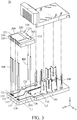
- FIG. 3 is an exploded view of the transmission assembly of FIG. 2
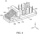
- FIG. 4 is a schematic view of the assembly of FIG. 3 .
- a connector 1 e.g. A RJ45 connector
- the insulated housing 10 comprises a main body 12, a top cover 14 and a back cover 16.
- the main body 12 has a slot 12a and an accommodating notch 12b.
- the slot 12a is configured for being plugged in by another connector (not shown in the figures).
- the accommodating notch 12b connects to the slot 12a, and the transmission assembly 20 is located in the accommodating notch 12b.
- the top cover 14 is installed on the main body 12 and covers the transmission assembly 20.
- a back cover 16 is installed on the main body 12 while the back cover 16 and the main body 12 abut on two opposite sides of the main circuit board 100.
- the transmission assembly 20 comprises a main circuit board 100, an expanded circuit board 200, a plurality of the first terminal 300, at least one the second terminal 400 and a plurality of the piercing terminals 500.
- the main circuit board 100 has a surface 110 and a transmission circuit 120 located on the surface 110.
- the expanded circuit board 200 is stacked on the surface 110 and has a top surface 210, a first lateral side 220, a second lateral side 230, an expanded circuit 240, a plurality of the first electrical contact 250, two second electrical contacts 260 and a transmission circuit 120.
- the first lateral side 220 and the second lateral side 230 are connected to opposite two sides of the top surface 210, respectively.
- the first lateral side 220 has a plurality of the first recessed portions 221, while the second lateral side 230 has two second recessed portions 231.
- the expanded circuit 240 is disposed on the top surface 210.
- the expanded circuit 240 is, for example, a noise suppression circuit.
- the first electrical contact 250 and the second electrical contact 260 are, for example, metal films and are electrically connected to the expanded circuit 240 respectively. These first electrical contacts 250 are formed on the wall surface of these first recessed portions 221. The two first electrical contacts 250 are formed on the wall surface of the two first recessed portions 221, respectively. The two second electrical contacts 260 are formed on the wall surface of the two second recessed portions 231, respectively.
- the number of the first electrical contacts 250 is six, while the number of the second electrical contacts 260 is two, but the disclosure is not limited thereto. In other embodiments, the numbers of the first electrical contacts 250 and the second electrical contacts 260 can be any numbers as long as the sum of them is eight.
- the number of the first terminals 300 is six and these first terminals 300 are arranged along a first line L1.
- Each first terminal 300 bends and forms a first limit section 310 and a first contact section 320.
- One end of the first limit section 310 is plugged in the main circuit board 100, while the other end is in electrical contact with the first electrical contact 250, for expanding the freedom of movement of the expanded circuit board 200 along a horizontal direction (namely positive x-axis direction).
- These first contact sections 320 extend from the first limit section 310 towards the second lateral side 230, and an obtuse angle is formed between the first contact section 320 and the first limit section 310.
- the number of the second terminals 400 is two and theses two second terminals 400 are arranged along a second line L2 parallel to the first line L1.
- Each second terminal 400 bends and forms a second limit section 410 and a second contact section 420.
- One end of the second limit section 410 is plugged in the main circuit board 100, while the other end is in electrical contact with the second electrical contact 260, for expanding the freedom of movement of the expanded circuit board 200 along another horizontal direction (namely negative x-axis direction).
- These second contact sections 420 bend and extend from the second limit section 410 towards the first lateral side 220 and is pressed against the top surface 210 of the expanded circuit board 200 for limiting the freedom of movement of the expanded circuit board 200 along a vertical direction (namely z-axis direction)
- the first contact section 320 and the second contact section 420 are exposed from the slot 12a and are in electrical contact with another connector (not shown in the figures).
- the height of the end of the second contact section 420 away from the first limit section 310 is designed to be lower than the top surface 210 of the expanded circuit board 200.
- each first electrical contact 250 is formed on each first recessed portion 221 while each second electrical contact 260 is formed on each second recessed portion 231.
- the first terminal 300 is also fastened with each first recessed portion 221.
- the two second terminals 400 are also fastened with the two second recessed portions 231, thereby limiting the freedom of movement of the expanded circuit board 200 along another horizontal direction (namely negative y-axis direction).
- the number of the first terminals 300 is six while the number of the second terminals 400 is two, but they are not limited thereto. In other embodiments, the numbers of the first terminal 300 and the second terminal 400 can be any numbers as long as the sum of them is eight.
- the plurality of the piercing terminal 500 is plugged in the main circuit board 100, and is electrically connected to each first terminal 300 and the two second terminals 400 respectively, via the transmission circuit 120. These piercing terminals 500 are used for being plugged by a transmission cable (not shown). When the transmission cable is plugged in the piercing terminal 500, the piercing terminal 500 pierces the insulation surface of the transmission cable for direct electrical connection with the conductive circuit on the outer part of the transmission cable.
- fixing and electrical connection can be achieved via the first limit section 310 of each first terminal 300, the first contact section 320, the second limit section 410 of each second terminal 400 and the second contact section 420.
- the welding process is not required in the assembly process so that the efficiency of the assembly of the connector 1 is improved.
- electrically connecting the expanded circuit 240 with the transmission circuit 120 via each first terminal 300 and each second terminal 400 can limit crosstalk interference and electromagnetic interference while the transmission circuit 120 is transmitting the signal.
- the expanded circuit board 200 when being plugged into or being separated from another connector, since the expanded circuit board 200 is fixed to the main circuit board 100 by each first terminal 300 and each second terminal 400, the expanded circuit board 200 does not swing with each first terminal 300 and each second terminal 400, thereby not increasing the possibility of the disconnection between the expanded circuit board 200 and each first terminal 300 as well as each second terminal 400. In contrast, this enhances the reliability of the connection structure between the main circuit board 100 and the expanded circuit board 200 when another connector is plugged in.
- FIG. 5A is a partial top view of the transmission assembly of FIG. 4 .
- the total number of the first terminals 300 and the second terminal 400 is eight.
- the main circuit board 100 has a first socket 131 to an eighth socket 138 along the positive y-axis direction.
- Six first terminal 300 are plugged in the first socket 131, the second socket 132, the third socket 133, the fifth socket 135, the seventh socket 137 and the eighth socket 138 respectively, while two second terminals 400 are plugged in the fourth socket 134 and the sixth socket 136 respectively. That is, in this embodiment, one of the first terminals 300 is between the two second terminals 400, but the disclosure is not limited thereto.
- FIG. 5B is a partial top view of the transmission assembly according to the second embodiment of the disclosure.
- the total number of the first terminals 300 and the second terminal 400 is eight.
- the main circuit board 100 has a first socket 131 to an eighth socket 138 along the positive y-axis direction.
- Six first terminals 300 are plugged in the first socket 131, the second socket 132, the fourth socket 134, the sixth socket 136, the seventh socket 137 and the eighth socket 138 respectively, while two second terminals 400 are plugged in the third socket 133 and the fifth socket 135 respectively.
- one of the first terminals 300 is between the two second terminals 400.
- FIG. 5C is a partial top view of the transmission assembly according to the third embodiment of the disclosure.
- the total number of the first terminals 300 and the second terminal 400 is eight.
- the main circuit board 100 has a first socket 131 to an eighth socket 138 along the positive y-axis direction.
- Six first terminals 300 are plugged in the first socket 131, the second socket 132, the fourth socket 134, the fifth socket 135, the seventh socket 137 and the eighth socket 138 respectively, while two second terminals 400 are plugged in the third socket 133 and the sixth socket 136 respectively.
- two of the first terminals 300 are between the two second terminals 400.
- FIG. 5D is a partial top view of the transmission assembly according to the fourth embodiment of the disclosure.
- the total number of the first terminals 300 and the second terminals 400 is eight.
- the main circuit board 100 has a first socket 131 to an eighth socket 138 along the positive y-axis direction.
- Six first terminals 300 are plugged in the first socket 131, the second socket 132, the third socket 133, the sixth socket 136, the seventh socket 137 and the eighth socket 138 respectively, while two second terminals 400 are plugged in the fourth socket 134 and the fifth socket 135 respectively.
- the two second terminals 400 are adjacent to each other.
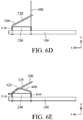
- FIG. 6A to FIG. 6E are schematic side views of the assembly process of the transmission assembly of FIG. 4 .
- first terminals 300 are plugged in the main circuit board 100.
- two second terminals 400 are plugged in the main circuit board 100.
- each first recessed portion 221 and each second recessed portion 231 of the expanded circuit board 200 slide along extending paths of each first terminal 300 and two second terminals 400 to stack on the main circuit board 100 of the expanded circuit board 200, while the expanded circuit board 200 is disposed between these first terminals 300 and the two second terminals 400.
- these first terminals 300 are bent for making each of them form a first limit section 310 and a first contact section 320.
- These first limit sections 310 are in electrical contact with the first electrical contacts 250 of the expanded circuit board 200 respectively, and the first contact sections 320 extend towards the second lateral side 230.
- two second terminals 400 are bent for making each of them form a second limit section 410 and a second contact section 420.
- the two second limit sections 410 are in electrical contact with the second electrical contact 260 respectively.
- the second contact section 420 extends towards the first lateral side 220 and is pressed against one side of the expanded circuit board 200 away from the main circuit board 100, thereby completing the assembly of the transmission assembly 20.
- bending the first terminal 300 before bending the second terminal 400 is not intended to limit the disclosure. In one embodiment, it is possible that the first terminal 300 is bent after the second terminal 400 is bent.
- the expanded circuit board is directly fixed to and electrically connected to the main circuit board via the first terminal and the second terminal.
- the welding process is not required in the assembly process so that the efficiency of the assembly of the connector is improved.
- the expanded circuit board can be a support plate for the first terminal and the second terminal while being disposed between them.
- plugging another connector into this connector or separating another connector from this connector may enhance the connection structure of the main circuit board and the expanded circuit board.
Landscapes
- Engineering & Computer Science (AREA)
- Microelectronics & Electronic Packaging (AREA)
- Manufacturing & Machinery (AREA)
- Coupling Device And Connection With Printed Circuit (AREA)
Claims (9)
- Connecteur (1) comprenant :un logement isolé (10) présentant une fente (12a) ; etun ensemble de transmission (20) situé dans le logement isolé (10), dans lequel l'ensemble de transmission (20) comprend une carte de circuit imprimé principal (100), une carte de circuit imprimé développé (200), une pluralité de premiers terminaux (300) et au moins un second terminal (400), la carte de circuit imprimé développé (200) a une surface supérieure (210), un premier côté latéral (220) et un second côté latéral (230), dans lequel la carte de circuit imprimé développé (200) est agencée sur la carte de circuit imprimé principal (100) et le premier côté latéral (220) et le second côté latéral (230) de la carte de circuit imprimé développé (200) qui sont en regard l'un de l'autre, ont une pluralité de premiers contacts électriques (250) et au moins un second contact électrique (260) respectivement, et les premiers terminaux (300) et l'au moins un second terminal (400) sont branchés dans la carte de circuit imprimé principal (100), dans lequel les premiers terminaux (300) plient et forment une première section limite (310) et une première section de contact (320), l'au moins un second terminal (400) plie etforme une seconde section limite (410) et une seconde section de contact (420), une extrémité, de chaque première section limite (310) et une extrémité de la seconde section limite (410) sont branchées dans la carte de circuit imprimé principal (100) alors que la carte de circuit imprimé développé (200) est agencée entre les autres extrémités de la première section limite (310) et l'autre extrémité de la seconde section limite (410) qui sont en contact électrique avec les premiers contacts électriques (250) et le second contact électrique (260) respectivement et dans lequel au moins une partie de la seconde section de contact (420) s'étend vers le premier côté latéral de la carte de circuit imprimé développé et est pressée contre la surface supérieure (210) de la carte de circuit imprimé développé (200), fixant par là même la carte de circuit imprimé développé (200) à la carte de circuit imprimé principal (100) et amenant la carte de circuit imprimé développé (200) et la carte de circuit imprimé principal (100) à être reliées électriquement l'une à l'autre, dans lequel la somme des nombres des premiers contacts électriques (250) et du nombre de l'au moins un second contact électrique (260) est de huit, la somme du nombre des premiers terminaux (300) et du nombre de l'au moins un second terminal (400) est de huit, le premier côté latéral (220) de la carte de circuit imprimé développé (200) a au moins une première partie évidée (221), le second côté latéral (230) a au moins une seconde partie évidée (231), chaque premier contact électrique (250) est formé sur une au moins une première partie évidée (221) et chaque second contact électrique (260) est formé sur une au moins une seconde partie évidée (231).
- Connecteur selon la revendication 1, dans lequel le nombre de premiers contacts électriques (250) est de six, le nombre de l'au moins un second contact électrique (260) est de deux, le nombre des premiers terminaux (300) est de six, le nombre de l'au moins un second terminal (400) est de deux, les premiers terminaux (300) sont agencés dans une première ligne, les deux seconds terminaux (400) sont agencés dans une seconde ligne, et la première ligne et la seconde ligne sont parallèles l'une à l'autre.
- Connecteur (1) selon la revendication 2, dans lequel les deux seconds terminaux (400) sont adjacents l'un à l'autre.
- Connecteur (1) selon la revendication 2, dans lequel un des premiers terminaux (300) est entre les deux seconds terminaux (400).
- Connecteur (1) selon la revendication 2, dans lequel deux des premiers terminaux (300) sont entre les deux seconds terminaux (400).
- Connecteur (1) selon la revendication 1, dans lequel la carte de circuit imprimé principal (100) a une surface (110) et un circuit de transmission (120), la carte de circuit imprimé développé (200) est agencée sur la surface (110), la carte de circuit imprimé développé (200) a un circuit développé (240), le circuit de transmission (120) est relié électriquement au circuit développé (240) via les premiers terminaux (300), l'au moins un second terminal (400), les premiers contacts électriques (250) et le second contact électrique (260).
- Connecteur (1) selon la revendication 6, dans lequel l'ensemble de transmission (20) comprend en outre une pluralité de terminaux de perçage (500), et les terminaux de perçage (500) sont branchés dans la carte de circuit imprimé principal (100) et sont reliés électriquement au circuit de transmission (120).
- Connecteur (1) selon la revendication 1, dans lequel le logement isolé (10) comprend :un corps principal (12) présentant une encoche de logement (12b), la fente (12a) reliant l'encoche de logement (12b) alors que l'ensemble de transmission (20) est situé dans l'encoche de logement (12b) et la fente (12a) expose les premiers terminaux (300) et le second terminal (400) ;un couvercle supérieur (14) installé sur le corps principal (12) et couvrant l'ensemble de transmission (20) ;et un couvercle arrière (16) installé sur le corps principal (12) alors que le couvercle arrière (16) et le corps principal (12) butent ensemble contre deux côtés en regard de la carte de circuit imprimé principal (100).
- Procédé d'assemblage pour un ensemble de transmission (20) d'un connecteur (1), comprenant les étapes de :branchement d'une pluralité de premiers terminaux (300) dans une carte de circuit imprimé principal (100) ;branchement au moins d'un second terrrairlal (400) dans la carte de circuit imprimé principal (100), caractérisé par
l'agencement d'une carte de circuit imprimé développé (200) sur la carte de circuit imprimé principal (100) dans lequel un premier côté latéral (220) et un second côté latéral (230) de la carte de circuit imprimé développé (200) qui sont en regard l'un de l'autre ont une pluralité de premiers contacts électriques (250) et au moins un second contact électrique (260) respectivement, la carte de circuit imprimé développé (200) est agencée entre les premiers terminaux (300) et le second terminal (400), le premier côté latéral (220) de la carte de circuit imprimé développé (200) a au moins une première partie évidée (221), le second côté latéral (230) a au moins une seconde partie évidée (231), les premiers contacts électriques (250) sont formés sur l'au moins une première partie évidée (221), et les seconds contacts électriques (260) sont formés sur l'au moins une seconde partie évidée (231) ; le pliage des premiers terminaux (300) de sorte que les premiers terminaux (300) forment chacun une première section limite (310) et une première section de contact (320), dans lequel les premières sections limites (310) sont en contact électrique avec les premiers contacts électriques (250) respectivement, et les première sections de contact (320) s'étendent vers le second côté latéral (230) ;
et
le pliage du second terminal (400) de sorte qu'il forme une seconde section limite (410) et une seconde section de contact (420), dans lequel la seconde section limite (410) est en contact électrique avec le second contact électrique (260) alors que la seconde section de contact (420) s'étend vers le premier côté latéral (220) et est pressée contre un côté de la carte de circuit imprimé développé (200) loin de la carte de circuit imprimé principal (100).
Priority Applications (2)
| Application Number | Priority Date | Filing Date | Title |
|---|---|---|---|
| PL14158703T PL2919326T3 (pl) | 2014-03-11 | 2014-03-11 | Złączka i sposób montażu zespołu przesyłania w złączce |
| EP14158703.0A EP2919326B1 (fr) | 2014-03-11 | 2014-03-11 | Connecteur et procédé d'assemblage pour ensemble de transmission de connecteur |
Applications Claiming Priority (1)
| Application Number | Priority Date | Filing Date | Title |
|---|---|---|---|
| EP14158703.0A EP2919326B1 (fr) | 2014-03-11 | 2014-03-11 | Connecteur et procédé d'assemblage pour ensemble de transmission de connecteur |
Publications (2)
| Publication Number | Publication Date |
|---|---|
| EP2919326A1 EP2919326A1 (fr) | 2015-09-16 |
| EP2919326B1 true EP2919326B1 (fr) | 2017-02-22 |
Family
ID=50239482
Family Applications (1)
| Application Number | Title | Priority Date | Filing Date |
|---|---|---|---|
| EP14158703.0A Active EP2919326B1 (fr) | 2014-03-11 | 2014-03-11 | Connecteur et procédé d'assemblage pour ensemble de transmission de connecteur |
Country Status (2)
| Country | Link |
|---|---|
| EP (1) | EP2919326B1 (fr) |
| PL (1) | PL2919326T3 (fr) |
Families Citing this family (1)
| Publication number | Priority date | Publication date | Assignee | Title |
|---|---|---|---|---|
| FR3078591B1 (fr) * | 2018-03-02 | 2021-11-05 | Delphi Int Operations Luxembourg Sarl | Prise de charge et procede de montage d'une telle prise sur un cable electrique |
Citations (1)
| Publication number | Priority date | Publication date | Assignee | Title |
|---|---|---|---|---|
| US5857858A (en) * | 1996-12-23 | 1999-01-12 | General Electric Company | Demountable and repairable low pitch interconnect for stacked multichip modules |
Family Cites Families (6)
| Publication number | Priority date | Publication date | Assignee | Title |
|---|---|---|---|---|
| JP2004222486A (ja) * | 2002-12-27 | 2004-08-05 | Murata Mfg Co Ltd | スイッチング電源モジュール |
| US7040927B1 (en) * | 2005-06-28 | 2006-05-09 | Lankom Electronics Co., Ltd. | Modular communications socket |
| US7794286B2 (en) * | 2008-12-12 | 2010-09-14 | Hubbell Incorporated | Electrical connector with separate contact mounting and compensation boards |
| US8052482B1 (en) * | 2010-10-28 | 2011-11-08 | Jyh Eng Technology Co., Ltd. | Female electrical connector |
| EP2487761B1 (fr) * | 2011-02-10 | 2013-07-31 | 3M Innovative Properties Company | Connecteur de télécommunication |
| US8496500B1 (en) * | 2012-02-14 | 2013-07-30 | Telebox Industries Corp. | Terminal holder structure for RJ45 dual-port jack |
-
2014
- 2014-03-11 PL PL14158703T patent/PL2919326T3/pl unknown
- 2014-03-11 EP EP14158703.0A patent/EP2919326B1/fr active Active
Patent Citations (1)
| Publication number | Priority date | Publication date | Assignee | Title |
|---|---|---|---|---|
| US5857858A (en) * | 1996-12-23 | 1999-01-12 | General Electric Company | Demountable and repairable low pitch interconnect for stacked multichip modules |
Also Published As
| Publication number | Publication date |
|---|---|
| EP2919326A1 (fr) | 2015-09-16 |
| PL2919326T3 (pl) | 2017-10-31 |
Similar Documents
| Publication | Publication Date | Title |
|---|---|---|
| US9787009B2 (en) | Receptacle connector having an insulating tongue with a combining area for accommodating combining portions of a plurality of contacts | |
| US9893481B2 (en) | Communications jack having a flexible substrate with a cantilevered finger with a crosstalk compensation circuit | |
| EP2184810B1 (fr) | Connecteur de carte | |
| US10276982B2 (en) | Electrical connector | |
| EP2487761B1 (fr) | Connecteur de télécommunication | |
| KR20110022569A (ko) | 전기 커넥터 | |
| CN101938053A (zh) | 多极连接器 | |
| US8449322B2 (en) | Electrical connector | |
| US9768559B2 (en) | Shield housing and socket connector | |
| US9130329B1 (en) | Connector and assembly method for transmission assembly of connector | |
| CN101183753A (zh) | 扁平缆线用电连接器 | |
| EP1753093B1 (fr) | Connecteur de télécommunications | |
| JP6097165B2 (ja) | コネクタ | |
| CN102157839B (zh) | 电连接器 | |
| EP2919326A1 (fr) | Connecteur et procédé d'assemblage pour ensemble de transmission de connecteur | |
| CN104733928B (zh) | 电连接器 | |
| CN101527415B (zh) | 电子转接装置 | |
| EP2624377B1 (fr) | Adaptateur de communication | |
| US9281622B2 (en) | Communications jacks having low-coupling contacts | |
| KR20220112665A (ko) | 기판 커넥터 | |
| TWI493813B (zh) | 電連接器 | |
| KR200278497Y1 (ko) | 고속통신용 케이블 커넥터 어셈블리의 케이블 고정구조 | |
| GB2510675A (en) | Communications jacks with contacts mounted on springs | |
| CN102570220A (zh) | 连接装置 | |
| JP2010010030A (ja) | シールド用ケース及び該シールド用ケースを用いた電気コネクタ |
Legal Events
| Date | Code | Title | Description |
|---|---|---|---|
| PUAI | Public reference made under article 153(3) epc to a published international application that has entered the european phase |
Free format text: ORIGINAL CODE: 0009012 |
|
| 17P | Request for examination filed |
Effective date: 20150522 |
|
| AK | Designated contracting states |
Kind code of ref document: A1 Designated state(s): AL AT BE BG CH CY CZ DE DK EE ES FI FR GB GR HR HU IE IS IT LI LT LU LV MC MK MT NL NO PL PT RO RS SE SI SK SM TR |
|
| AX | Request for extension of the european patent |
Extension state: BA ME |
|
| REG | Reference to a national code |
Ref country code: DE Ref legal event code: R079 Ref document number: 602014006844 Country of ref document: DE Free format text: PREVIOUS MAIN CLASS: H01R0012520000 Ipc: H05K0001140000 |
|
| GRAP | Despatch of communication of intention to grant a patent |
Free format text: ORIGINAL CODE: EPIDOSNIGR1 |
|
| RIC1 | Information provided on ipc code assigned before grant |
Ipc: H05K 1/14 20060101AFI20160922BHEP Ipc: H01R 24/64 20110101ALI20160922BHEP Ipc: H05K 3/40 20060101ALI20160922BHEP Ipc: H01R 13/6469 20110101ALI20160922BHEP Ipc: H01R 12/52 20110101ALI20160922BHEP Ipc: H01R 13/6466 20110101ALI20160922BHEP Ipc: H05K 3/36 20060101ALI20160922BHEP Ipc: H01R 13/6467 20110101ALI20160922BHEP |
|
| INTG | Intention to grant announced |
Effective date: 20161027 |
|
| GRAS | Grant fee paid |
Free format text: ORIGINAL CODE: EPIDOSNIGR3 |
|
| GRAA | (expected) grant |
Free format text: ORIGINAL CODE: 0009210 |
|
| AK | Designated contracting states |
Kind code of ref document: B1 Designated state(s): AL AT BE BG CH CY CZ DE DK EE ES FI FR GB GR HR HU IE IS IT LI LT LU LV MC MK MT NL NO PL PT RO RS SE SI SK SM TR |
|
| REG | Reference to a national code |
Ref country code: GB Ref legal event code: FG4D |
|
| REG | Reference to a national code |
Ref country code: CH Ref legal event code: EP |
|
| REG | Reference to a national code |
Ref country code: AT Ref legal event code: REF Ref document number: 870177 Country of ref document: AT Kind code of ref document: T Effective date: 20170315 |
|
| REG | Reference to a national code |
Ref country code: IE Ref legal event code: FG4D |
|
| REG | Reference to a national code |
Ref country code: CH Ref legal event code: NV Representative=s name: LANGPATENT ANWALTSKANZLEI IP LAW FIRM, CH |
|
| REG | Reference to a national code |
Ref country code: DE Ref legal event code: R096 Ref document number: 602014006844 Country of ref document: DE |
|
| REG | Reference to a national code |
Ref country code: LT Ref legal event code: MG4D |
|
| REG | Reference to a national code |
Ref country code: NL Ref legal event code: MP Effective date: 20170222 |
|
| REG | Reference to a national code |
Ref country code: AT Ref legal event code: MK05 Ref document number: 870177 Country of ref document: AT Kind code of ref document: T Effective date: 20170222 |
|
| PG25 | Lapsed in a contracting state [announced via postgrant information from national office to epo] |
Ref country code: FI Free format text: LAPSE BECAUSE OF FAILURE TO SUBMIT A TRANSLATION OF THE DESCRIPTION OR TO PAY THE FEE WITHIN THE PRESCRIBED TIME-LIMIT Effective date: 20170222 Ref country code: GR Free format text: LAPSE BECAUSE OF FAILURE TO SUBMIT A TRANSLATION OF THE DESCRIPTION OR TO PAY THE FEE WITHIN THE PRESCRIBED TIME-LIMIT Effective date: 20170523 Ref country code: NO Free format text: LAPSE BECAUSE OF FAILURE TO SUBMIT A TRANSLATION OF THE DESCRIPTION OR TO PAY THE FEE WITHIN THE PRESCRIBED TIME-LIMIT Effective date: 20170522 Ref country code: LT Free format text: LAPSE BECAUSE OF FAILURE TO SUBMIT A TRANSLATION OF THE DESCRIPTION OR TO PAY THE FEE WITHIN THE PRESCRIBED TIME-LIMIT Effective date: 20170222 Ref country code: HR Free format text: LAPSE BECAUSE OF FAILURE TO SUBMIT A TRANSLATION OF THE DESCRIPTION OR TO PAY THE FEE WITHIN THE PRESCRIBED TIME-LIMIT Effective date: 20170222 |
|
| PG25 | Lapsed in a contracting state [announced via postgrant information from national office to epo] |
Ref country code: NL Free format text: LAPSE BECAUSE OF NON-PAYMENT OF DUE FEES Effective date: 20170222 Ref country code: SE Free format text: LAPSE BECAUSE OF FAILURE TO SUBMIT A TRANSLATION OF THE DESCRIPTION OR TO PAY THE FEE WITHIN THE PRESCRIBED TIME-LIMIT Effective date: 20170222 Ref country code: LV Free format text: LAPSE BECAUSE OF FAILURE TO SUBMIT A TRANSLATION OF THE DESCRIPTION OR TO PAY THE FEE WITHIN THE PRESCRIBED TIME-LIMIT Effective date: 20170222 Ref country code: BG Free format text: LAPSE BECAUSE OF FAILURE TO SUBMIT A TRANSLATION OF THE DESCRIPTION OR TO PAY THE FEE WITHIN THE PRESCRIBED TIME-LIMIT Effective date: 20170522 Ref country code: AT Free format text: LAPSE BECAUSE OF FAILURE TO SUBMIT A TRANSLATION OF THE DESCRIPTION OR TO PAY THE FEE WITHIN THE PRESCRIBED TIME-LIMIT Effective date: 20170222 Ref country code: PT Free format text: LAPSE BECAUSE OF FAILURE TO SUBMIT A TRANSLATION OF THE DESCRIPTION OR TO PAY THE FEE WITHIN THE PRESCRIBED TIME-LIMIT Effective date: 20170622 Ref country code: RS Free format text: LAPSE BECAUSE OF FAILURE TO SUBMIT A TRANSLATION OF THE DESCRIPTION OR TO PAY THE FEE WITHIN THE PRESCRIBED TIME-LIMIT Effective date: 20170222 Ref country code: ES Free format text: LAPSE BECAUSE OF FAILURE TO SUBMIT A TRANSLATION OF THE DESCRIPTION OR TO PAY THE FEE WITHIN THE PRESCRIBED TIME-LIMIT Effective date: 20170222 |
|
| PG25 | Lapsed in a contracting state [announced via postgrant information from national office to epo] |
Ref country code: RO Free format text: LAPSE BECAUSE OF FAILURE TO SUBMIT A TRANSLATION OF THE DESCRIPTION OR TO PAY THE FEE WITHIN THE PRESCRIBED TIME-LIMIT Effective date: 20170222 Ref country code: IT Free format text: LAPSE BECAUSE OF FAILURE TO SUBMIT A TRANSLATION OF THE DESCRIPTION OR TO PAY THE FEE WITHIN THE PRESCRIBED TIME-LIMIT Effective date: 20170222 Ref country code: CZ Free format text: LAPSE BECAUSE OF FAILURE TO SUBMIT A TRANSLATION OF THE DESCRIPTION OR TO PAY THE FEE WITHIN THE PRESCRIBED TIME-LIMIT Effective date: 20170222 Ref country code: EE Free format text: LAPSE BECAUSE OF FAILURE TO SUBMIT A TRANSLATION OF THE DESCRIPTION OR TO PAY THE FEE WITHIN THE PRESCRIBED TIME-LIMIT Effective date: 20170222 Ref country code: SK Free format text: LAPSE BECAUSE OF FAILURE TO SUBMIT A TRANSLATION OF THE DESCRIPTION OR TO PAY THE FEE WITHIN THE PRESCRIBED TIME-LIMIT Effective date: 20170222 |
|
| REG | Reference to a national code |
Ref country code: DE Ref legal event code: R097 Ref document number: 602014006844 Country of ref document: DE |
|
| PG25 | Lapsed in a contracting state [announced via postgrant information from national office to epo] |
Ref country code: SM Free format text: LAPSE BECAUSE OF FAILURE TO SUBMIT A TRANSLATION OF THE DESCRIPTION OR TO PAY THE FEE WITHIN THE PRESCRIBED TIME-LIMIT Effective date: 20170222 Ref country code: MC Free format text: LAPSE BECAUSE OF FAILURE TO SUBMIT A TRANSLATION OF THE DESCRIPTION OR TO PAY THE FEE WITHIN THE PRESCRIBED TIME-LIMIT Effective date: 20170222 Ref country code: DK Free format text: LAPSE BECAUSE OF FAILURE TO SUBMIT A TRANSLATION OF THE DESCRIPTION OR TO PAY THE FEE WITHIN THE PRESCRIBED TIME-LIMIT Effective date: 20170222 |
|
| REG | Reference to a national code |
Ref country code: IE Ref legal event code: MM4A |
|
| PLBE | No opposition filed within time limit |
Free format text: ORIGINAL CODE: 0009261 |
|
| REG | Reference to a national code |
Ref country code: FR Ref legal event code: ST Effective date: 20171130 |
|
| STAA | Information on the status of an ep patent application or granted ep patent |
Free format text: STATUS: NO OPPOSITION FILED WITHIN TIME LIMIT |
|
| 26N | No opposition filed |
Effective date: 20171123 |
|
| PG25 | Lapsed in a contracting state [announced via postgrant information from national office to epo] |
Ref country code: FR Free format text: LAPSE BECAUSE OF NON-PAYMENT OF DUE FEES Effective date: 20170424 Ref country code: LU Free format text: LAPSE BECAUSE OF NON-PAYMENT OF DUE FEES Effective date: 20170311 |
|
| PG25 | Lapsed in a contracting state [announced via postgrant information from national office to epo] |
Ref country code: SI Free format text: LAPSE BECAUSE OF FAILURE TO SUBMIT A TRANSLATION OF THE DESCRIPTION OR TO PAY THE FEE WITHIN THE PRESCRIBED TIME-LIMIT Effective date: 20170222 Ref country code: IE Free format text: LAPSE BECAUSE OF NON-PAYMENT OF DUE FEES Effective date: 20170311 |
|
| REG | Reference to a national code |
Ref country code: BE Ref legal event code: MM Effective date: 20170331 |
|
| PG25 | Lapsed in a contracting state [announced via postgrant information from national office to epo] |
Ref country code: BE Free format text: LAPSE BECAUSE OF NON-PAYMENT OF DUE FEES Effective date: 20170331 |
|
| PG25 | Lapsed in a contracting state [announced via postgrant information from national office to epo] |
Ref country code: MT Free format text: LAPSE BECAUSE OF NON-PAYMENT OF DUE FEES Effective date: 20170311 |
|
| GBPC | Gb: european patent ceased through non-payment of renewal fee |
Effective date: 20180311 |
|
| PG25 | Lapsed in a contracting state [announced via postgrant information from national office to epo] |
Ref country code: GB Free format text: LAPSE BECAUSE OF NON-PAYMENT OF DUE FEES Effective date: 20180311 |
|
| PG25 | Lapsed in a contracting state [announced via postgrant information from national office to epo] |
Ref country code: HU Free format text: LAPSE BECAUSE OF FAILURE TO SUBMIT A TRANSLATION OF THE DESCRIPTION OR TO PAY THE FEE WITHIN THE PRESCRIBED TIME-LIMIT; INVALID AB INITIO Effective date: 20140311 |
|
| PG25 | Lapsed in a contracting state [announced via postgrant information from national office to epo] |
Ref country code: CY Free format text: LAPSE BECAUSE OF FAILURE TO SUBMIT A TRANSLATION OF THE DESCRIPTION OR TO PAY THE FEE WITHIN THE PRESCRIBED TIME-LIMIT Effective date: 20170222 |
|
| PG25 | Lapsed in a contracting state [announced via postgrant information from national office to epo] |
Ref country code: MK Free format text: LAPSE BECAUSE OF FAILURE TO SUBMIT A TRANSLATION OF THE DESCRIPTION OR TO PAY THE FEE WITHIN THE PRESCRIBED TIME-LIMIT Effective date: 20170222 |
|
| PG25 | Lapsed in a contracting state [announced via postgrant information from national office to epo] |
Ref country code: TR Free format text: LAPSE BECAUSE OF FAILURE TO SUBMIT A TRANSLATION OF THE DESCRIPTION OR TO PAY THE FEE WITHIN THE PRESCRIBED TIME-LIMIT Effective date: 20170222 |
|
| PG25 | Lapsed in a contracting state [announced via postgrant information from national office to epo] |
Ref country code: AL Free format text: LAPSE BECAUSE OF FAILURE TO SUBMIT A TRANSLATION OF THE DESCRIPTION OR TO PAY THE FEE WITHIN THE PRESCRIBED TIME-LIMIT Effective date: 20170222 Ref country code: IS Free format text: LAPSE BECAUSE OF FAILURE TO SUBMIT A TRANSLATION OF THE DESCRIPTION OR TO PAY THE FEE WITHIN THE PRESCRIBED TIME-LIMIT Effective date: 20170622 |
|
| P01 | Opt-out of the competence of the unified patent court (upc) registered |
Effective date: 20230601 |
|
| PGFP | Annual fee paid to national office [announced via postgrant information from national office to epo] |
Ref country code: CH Payment date: 20250401 Year of fee payment: 12 |
|
| REG | Reference to a national code |
Ref country code: CH Ref legal event code: U11 Free format text: ST27 STATUS EVENT CODE: U-0-0-U10-U11 (AS PROVIDED BY THE NATIONAL OFFICE) Effective date: 20260401 |
|
| PGFP | Annual fee paid to national office [announced via postgrant information from national office to epo] |
Ref country code: DE Payment date: 20260121 Year of fee payment: 13 |
|
| PGFP | Annual fee paid to national office [announced via postgrant information from national office to epo] |
Ref country code: PL Payment date: 20260121 Year of fee payment: 13 |