EP2919404A1 - Multiplexsystem und System zum Demultiplexen für WDM-Kanalübertragung - Google Patents
Multiplexsystem und System zum Demultiplexen für WDM-Kanalübertragung Download PDFInfo
- Publication number
- EP2919404A1 EP2919404A1 EP14305343.7A EP14305343A EP2919404A1 EP 2919404 A1 EP2919404 A1 EP 2919404A1 EP 14305343 A EP14305343 A EP 14305343A EP 2919404 A1 EP2919404 A1 EP 2919404A1
- Authority
- EP
- European Patent Office
- Prior art keywords
- optical
- channel
- channels
- input
- multiplexer
- Prior art date
- Legal status (The legal status is an assumption and is not a legal conclusion. Google has not performed a legal analysis and makes no representation as to the accuracy of the status listed.)
- Granted
Links
Images


Classifications
-
- H—ELECTRICITY
- H04—ELECTRIC COMMUNICATION TECHNIQUE
- H04J—MULTIPLEX COMMUNICATION
- H04J14/00—Optical multiplex systems
- H04J14/02—Wavelength-division multiplex systems
- H04J14/0201—Add-and-drop multiplexing
- H04J14/0202—Arrangements therefor
- H04J14/0208—Interleaved arrangements
-
- H—ELECTRICITY
- H04—ELECTRIC COMMUNICATION TECHNIQUE
- H04J—MULTIPLEX COMMUNICATION
- H04J14/00—Optical multiplex systems
- H04J14/02—Wavelength-division multiplex systems
- H04J14/0221—Power control, e.g. to keep the total optical power constant
Definitions
- the present document relates to multiplexing and demultiplexing systems.
- the present document relates to multiplexing and demultiplexing systems for transmission of WDM channels according to a WDM channel grid providing a high spectral efficiency.
- WDM channels can be combined either with optical couplers or with wavelength multiplexers.
- Optical couplers provide no filtering function, i.e. the full signal spectrum provided at the inputs is coupled to the output of the coupler.
- Using optical couplers for combining optical channels has some disadvantages.
- the attenuation caused by optical couplers increases with the number of channels to combine. For example, combining 100 channels leads to an attenuation of approximately 20dB. Said attenuation may be compensated by using optical amplifiers.
- adding optical amplifiers after the optical coupler leads to a poor OSNR (optical signal to noise ratio) because of low input power.
- OSNR optical signal to noise ratio
- Attenuation could also be compensated by adding optical amplifiers before the coupler, but here amplified spontaneous emission (ASE) noise recombination will degrade the optical signal noise ratio (OSNR) after the coupler.
- OSNR optical signal noise ratio
- Said multiplexer comprises a filter unit providing an optical filter function.
- the 3dB-bandwidth of said filter function is usually equal or slightly smaller than the channel spacing. This introduces channel distortions and thus degrades the system performance when bandwidth of the optical signal to be transmitted in an optical channel is very close to channel spacing.
- an optical multiplexing system comprises a first multiplexer, a second multiplexer and an optical coupler.
- Said first multiplexer comprises at least a first input for receiving a first optical channel set comprising one or more optical channels of an optical channel grid for a WDM system.
- the second multiplexer comprises at least a first input for receiving a second optical channel set comprising one or more optical channels of the optical WDM channel grid.
- the optical channels of the first and second channel set may be different optical channels of the optical channel grid.
- a channel set may include only one optical channel and inputs of the multiplexers each receive a single optical channel.
- a channel set is sometimes also called a group of channels.
- the first input of the first multiplexer receives a first optical channel
- the first input of the second multiplexer receives a second optical channel of the optical channel grid.
- a channel set may include a plurality of neighboring optical channels, i.e. optical channels having an adjacent frequency or wavelength in the optical channel grid.
- the first input of the first multiplexer receives a first set of contiguous optical channels
- the first input of the second multiplexer receives a second set of contiguous optical channels of the optical channel grid.
- the inputs of the optical coupler may be coupled with the outputs of the first and second multiplexer for combining and transmitting the first and second channel sets provided at the outputs of the multiplexers via a common optical transmission path.
- the optical channels of the WDM channel grid are distributed across the at least two multiplexers such that one channel of the first optical channel set and one channel of the second optical channel set are adjacent channels of the optical channel grid. If there is only a single channel in a channel set, the channel of the first optical channel set and the channel of the second optical channel set are adjacent channels, i.e. they are neighboring channels of the channel grid. In case of channel sets comprising a plurality of optical channels (2 or more channels per channel set; please note that the number of channels per channel set may differ and need not be identical), the last optical channel of the first optical channel set (in terms of frequency or wavelength) may be adjacent (in terms of frequency or wavelength) to the first optical channel of the second optical channel set. In other words, adjacent optical channels are assigned to different multiplexers.
- the first multiplexer comprises a first filter unit having a first filter function for filtering the optical signals of one or more optical channels received at the first input of the first multiplexer. If the first multiplexer has more than one input, a respective filter unit for each input may be provided.
- the second multiplexer comprises a second filter unit having a second filter function for filtering the optical signals of one or more optical channels received at the first input of the second multiplexer. If the second multiplexer has more than one input, a respective filter unit for each input may be provided.
- the filter units of the first and second multiplexers are configured such that the 3dB-bandwidths of the first and second filter functions are larger than the sum of the bandwidths of the channels that are associated to the respective input of the multiplexers.
- a cut-off of the edges of the signals associated with the respective channels can be avoided because the filter bandwidth of a filter function is broader than the (accumulated) signal bandwidth transmitted in the respective optical channel(s) associated with the filter, respectively, broader than the channel spacing or a respective multiple of the channel spacing if a channel set includes multiple channels arranged based on the channel spacing.
- the bandwidths of the first and second filter functions associated with the filter units of the first and second multiplexers partially overlap.
- adjacent optical channels are assigned to different multiplexers having respective filter functions, adjacent channels are not impaired (e.g.
- the configuration of the supplied optical signals is such that no adjacent channels are provided at any two inputs of one multiplexer to avoid signal degradations from overlapping filter functions.
- filter bandwidth of a filter function In order to cut off (remove) noise, e.g. due to ASE, from outside of the channel spectra, the extent to which the filter bandwidth of a filter function is broader than the (accumulated) signal bandwidth of the associated optical channel(s) should be limited and as small as possible .
- filter functions having a steep slope are employed.
- the overlap of filter functions associated with the filter units of the first and second multiplexers may be limited to the slopes of the filter functions, while the flat filter passbands do not or not significantly overlap.
- the spectrum of the optical signal(s) may have a rectangular shape or approximately a rectangular shape.
- pulse shaping units e.g. based on digital signal processing
- RRC Root Raised Cosine
- the spectrum is equal to 1.1 times the baudrate, which is sufficiently close to a rectangular spectrum.
- the roll-off is 0.01, the spectrum is equal to 1.01 times the baudrate, which is very close to a rectangular spectrum.
- a bandwidth of a filter function is defined as the frequency range outside which range the spectrum is being filtered out as a result of applying the filter function.
- the bandwidth of the filter function may be defined at a certain decrease (attenuation) of the filter transfer function, i.e., the 3dB-bandwidth is defined for 3dB attenuation, the 1dB-bandwidth for 1dB attenuation, and the 0.5dB-bandwidth for 0.5dB attenuation, etc.
- the filter functions of the filter units may be configured such as to overlap with their frequency ranges that correspond to the 1dB bandwidths or the 0.5dB-bandwidths of the first and second filter functions.
- the 1dB-bandwidths or the 0.5dB-bandwidths of the first and second filter functions overlap.
- the channels are filtered without distortion, while the overlap between bandwidths of the first and second filter functions remains small allowing high filtering of ASE noise.
- the bandwidths of the first and second filter functions start overlap at an attenuation lower than 3dB and overlap at attenuations 3dB and higher.
- the overlap of the filter functions may start between 0dB and 1dB attenuation level, and, preferably, between 0.5dB and 1dB attenuation level.
- the overlap of the bandwidths of the first and second filter functions is smaller than the channel spacing of the channel grid, or of the channel bandwidth.
- the overlap of the bandwidths of the first and second filter functions is smaller than 50% (1/2), 25% (1/4) or even 12.5% (1/8) of the channel spacing of the channel grid, or of the channel bandwidth.
- Limiting the overlap to one channel spacing or less is advantageous because, when filtering one channel, the overlap broader than the channel spacing would allow unfiltered noise on a frequency range of two channels adjacent to the filtered channel.
- the first and second multiplexers each comprise a wavelength selective switch (WSS) with free programmable filtering for each input of the first and second multiplexer.
- the WSS may be programmable according to a frequency pattern comprising discrete frequency steps.
- the filtering function provided to the optical signals received at each input of the WSS can be varied in discrete frequency steps.
- the frequency step is 6.25GHz or 12.5GHz (and could go reduced to 3.125GHz or possibly less in the near future).
- the filter function may, for example, comprise a filter bandwidth of 62.5GHz , i.e., 50GHz + 12.5GHz.
- the WSS may be programed to have a filter bandwidth of 206.25GHz or 212.5GHz, i.e., 4 x 50 GHz + 6.25GHz or 12.5 GHz.
- the first input of the first and/or second multiplexer(s) is/are coupled with an optical coupler for receiving multiple optical signals at a single input.
- the coupling of a multiplexer with an optical coupling may be via an optical amplifier.
- the optical coupler may comprise multiple inputs and may combine the optical signals received via said optical inputs and provide a single output signal comprising all spectral signal components of the received input signals, e.g. the adjacent WDM channels of a channel set. Said output signal may be provided to a single input of the multiplexer.
- the first multiplexer comprises at least a second input for receiving a further channel set, the further channel set being spaced from the first channel set provided at the first input of the first multiplexer by a spectral gap comprising a width of at least one channel spacing.
- at least a second filter unit may be provided in the first multiplexer to filter the signal received at its second input.
- each input of a multiplexer may have an associated filter unit.
- the second multiplexer may comprise at least a second input for receiving a further channel set, the further channel set being spaced from the first channel set provided at the first input of the second multiplexer by a spectral gap comprising a width of at least one channel spacing.
- Respective filter units for each multiplexer input may be provided. Thereby, the optical channels or sets of optical channels to be transmitted via a particular multiplexer are separated from each other in order to avoid a negative impact of overlapping of the filter function.
- the first and second multiplexers each comprise a plurality of inputs. Consecutive channel sets respectively comprising a group of successive channel signals may be alternately coupled with consecutive inputs of the first and second multiplexer. In case of only one signal/channel per channel set, consecutive channels may be alternately coupled with consecutive inputs of the first and second multiplexer.
- optical channels comprising an odd channel number may be transmitted via the first multiplexer and optical channels comprising an even channel number may be transmitted via the second multiplexer. Thereby, a spectral distribution of optical channels across multiple optical multiplexers is obtained. In an extension, more than 2 multiplexers can be used and adjacent optical channels are distributed across the multiplexers.
- the first filter function for filtering the optical signal at the first input of the first multiplexer comprises a filter bandwidth larger than the total signal bandwidth of the first optical channel set.
- the second filter function for filtering the optical signal at the first input of the second multiplexer may comprise a filter bandwidth larger than the total signal bandwidth of the second optical channel set.
- Total signal bandwidth refers to the target signal or information signal of a channel set without any side peaks or noise which have much lower energy than the information signal (e.g. more than 20dB lower).
- an optical transmission system comprises at least two optical transmitters to generate optical WDM signals to be arranged in adjacent optical channels of an optical channel grid and an optical multiplexing system described above.
- An output of a first optical transmitter is coupled with the first input of the first multiplexer and an output of a second optical transmitter is coupled with the first input of the second optical multiplexer.
- Said first optical transmitter may provide optical signals according to a first optical channel set comprising one or more optical channels and said second optical transmitter may provide optical signals according to a second optical channel set comprising one or more optical channels, wherein adjacent optical channels are at least partially transmitted via different optical multiplexers.
- an optical demultiplexing system which in general mirrors the multiplexing system described above.
- the optical demultiplexing system comprises an optical splitter for splitting an optical wavelength multiplexed signal received from an optical transmission path into at least two signal portions.
- the optical wavelength multiplexed signal comprises a plurality of optical signals corresponding to optical channels of an optical channel grid.
- the optical demultiplexing system comprises a first demultiplexer comprising an input connected to a first output of the optical splitter for receiving a first signal portion, and a second demultiplexer comprising an input connected to a second output of the optical splitter for receiving a second signal portion.
- the first demultiplexer comprises a first filter unit having a first filter function for filtering the optical signals received at its input in order to provide a first optical channel set comprising one or more optical channels at a first output of the first demultiplexer.
- the second demultiplexer comprises a second filter unit having a second filter function for filtering the optical signals received at its input in order to provide a second optical channel set comprising one or more optical channels at a first output of the second demultiplexer.
- the filter units of the respective optical demultiplexer are configured such that the bandwidths of the first and second filter functions overlap.
- the optical channels are distributed across the optical demultiplexers such that one channel of the first optical channel set and one channel of the second optical channel set are adjacent channels of the optical channel grid.
- the filter units of the first and second demultiplexers are configured such that the 3dB-bandwidths of the first and second filter functions are larger than the sum of the bandwidths of the channels that are associated to the respective output of the demultiplexers. Further, for example, the 1dB-bandwidths or the 0.5dB-bandwidths of the first and second filter functions partially overlap.
- the first and second demultiplexers each comprise a wavelength selective switch (WSS) with free programmable filtering for each output of the first and second demultiplexer.
- the WSS may be programmable according to a frequency pattern comprising discrete frequency steps.
- the filtering function provided on the optical signals to be output at the respective outputs of the WSS can be varied in discrete frequency steps.
- the frequency step is 6.25GHz or 12.5GHz. So, in a WDM environment with 50GHz channel spacing, the filter function may, for example, comprise a filter bandwidth of 62.5GHz.
- the first demultiplexer comprises at least a second output for providing a further channel set, the further channel set being spaced from the first channel set provided at the first output of the first demultiplexer by a spectral gap comprising a width of at least one channel spacing.
- a spectral gap comprising a width of at least one channel spacing.
- the second demultiplexer may comprise at least a second output for providing a further channel set, the further channel set being spaced from the first channel set provided at the first output of the second demultiplexer by a spectral gap comprising a width of at least one channel spacing.
- the configuration of the multiplexer filter functions is such that no adjacent channels are provided at any two outputs of one multiplexer to avoid signal degradations from overlapping filter functions.
- consecutive channels or consecutive channel sets are alternately provided at the outputs of the first and second demultiplexer.
- optical channels comprising an odd channel number may be transmitted via the first demultiplexer and optical channels comprising an even channel number may be transmitted via the second demultiplexer.
- the first filter function for filtering the one or more optical signals at the input of the first demultiplexer comprises a filter bandwidth larger than the total signal bandwidth of the first optical channel set.
- the second filter function for filtering the one or more optical signals at the input of the second demultiplexer may comprise a filter bandwidth larger than the total signal bandwidth of the second optical channel set.
- total signal bandwidth refers to the target signal or information signal without any side peaks or noise which have much lower energy than the target or information signal (e.g. more than 20dB lower).
- an optical receiving system comprises an optical demultiplexing system as described before and at least two coherent receivers for receiving the filtered optical signals from the outputs of the first and second demultiplexer.
- Coherent receivers allow a good channel selection so that a coherent receiver can be coupled to a demultiplexer output carrying a set of channels, and the coherent receiver can selectively receive the optical signal of one designated channel.
- an optical coupler/splitter may be interposed between demultiplexer and the receivers.
- the above described aspects and embodiments may also be implemented as a method for multiplexing optical channels of a WDM channel grid, or demultiplexing optical channels of the WDM channel grid.
- the multiplexing is based on assigning adjacent optical channels (i.e. channels that are next to each other in terms of frequency or wavelength) to inputs of different multiplexers.
- the filter functions of these inputs of the different multiplexers have a 3dB-bandwidth that is slightly broader than the signal/channel bandwidths of the channels that are associated with an input to avoid any impairment on the optical signals, and at the same time allow an arrangement of the optical channel in the optical grid without much gap or spacing between the channels. Further, the filter functions of these inputs of the different multiplexers may overlap.
- the output signals of the different multiplexers may then be combined by optical couplers.
- the demultiplexing method in general mirrors the multiplexing method as the skilled person understands.
- the first and second filter functions overlap within the frequency range of their respective 1dB-bandwidths or 0.5dB-bandwidths.
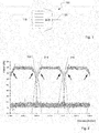
- Fig. 1 shows a schematic structure of an optical multiplexer 100.
- the optical multiplexer 100 comprises multiple optical inputs 110 for receiving optical input signals. Said optical input signals may be associated with optical channels of an optical WDM system. For example said optical channels may be arranged next to each other according to a fixed or flexible channel grid.
- the optical multiplexer 100 further comprises an optical output 120.
- the optical multiplexer 100 is adapted to receive the optical input signals provided at the optical inputs 110, combine said optical input signals into a single optical output signal and output said optical output signal at the optical output 120, wherein the optical output signal comprises spectral components of all optical input signals.
- the optical multiplexer 100 may be adapted to filter the optical input signals.
- the optical multiplexer 100 may comprise one or more optical filter units.
- the one or more optical filter units may implement one or more optical filter functions 210.
- Said one or more optical filter units may be used to filter the optical input signals according to the respective optical filter function 210 in order to filter out side bands of the optical signals.
- the bandwidth of the optical channels, respectively, the bandwidth of the optical signals associated with the optical channels are very close to the channel spacing, i.e. there is no or nearly no gap between adjacent channels.
- the symbol rate is very close to the channel spacing (e.g. 48Gbaud for 50GHz spacing or 32Gbaud for 33.3GHz spacing).
- RZ return-to-zero
- the spectrum width is relatively large and a narrow optical filtering is not inducing a significant penalty. But once the channel spacing is narrower that the symbol rate, penalties are induced.
- the optical filter functions associated with the respective optical channels in prior art systems comprise 3dB-bandwidths which are usually equal or slightly smaller than the channel spacing. Therefore, the side portions of the spectra of optical channels are attenuated (as indicated by arrows in Fig. 2 ), i.e. the optical channels are distorted which reduces the system performance significantly.
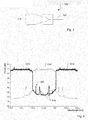
- Fig. 3 shows a possibility of combining optical input signals using an optical coupler 300.
- the optical coupler 300 comprises two or more optical inputs 310 for receiving optical input signals. Said optical input signals may be associated with optical channels of an optical WDM system.
- the optical coupler 300 further comprises an optical output 320.
- the optical coupler 300 is adapted to receive the optical input signals provided at the optical inputs 310, combine said optical input signals without filtering into a single optical output signal and output said optical output signal at the optical output 320, wherein the optical output signal comprises all optical input signals.
- optical couplers 300 comprise a significant optical attenuation (typically ⁇ 3dB).
- a plurality of optical couplers 300 may be cascaded. By cascading multiple optical couplers 300, the attenuation of the coupling arrangement may rise. For example, said attenuation may be 20dB for coupling 100 optical channels.
- a further disadvantage of using a plurality of optical couplers for combining a plurality of channels without any filtering is the increase of noise due to summing up amplified spontaneous emission (ASE) noise provided at the optical inputs 310 of the optical coupler 300.
- Said ASE may be caused by an optical amplifier coupled with the optical input 310 of the optical coupler 300.
- the optical signal to noise ratio (OSNR) provided at each optical input 310 of the optical coupler 300 may be 40dB.
- OSNR optical signal to noise ratio
- the resulting OSNR may be reduced significantly and performance of the optical transmission system is decreased.
- the number of cascaded couplers, respectively, the number of optical channels to be connected to an optical input 320 of an optical coupler 300 has to be limited in order to obtain an acceptable OSNR.
- a further disadvantage of using optical couplers 300 without any filtering of input signals are signal peaks 410, 420 within the channel bandwidth of a first optical channel CH1 caused by crosstalk from adjacent channels CH0, CH2.
- the signal peaks may be caused, e.g., by imperfections of digital-to-analog converters for generating the optical signals coupled with the optical inputs 310 of the optical coupler 300. Said imperfections may be caused by aliasing effects (peaks 420) or by imperfect interleaving of the different subDACs of a high speed DAC (peaks 410).
- Fig. 5 shows an optical transmission system 500 according to an embodiment.
- the system comprises at least two optical multiplexer, in the present example a first and a second multiplexer 510, 520.
- Each multiplexer 510, 520 may comprise multiple optical inputs 511, 521 for receiving optical input signals. Said optical input signals may be associated with optical channels of an optical WDM system.
- Each optical multiplexer 510, 520 may further comprise an optical output 512, 522.
- the optical multiplexers 510, 520 may be adapted to receive the optical input signals provided at the optical inputs 511, 521, filter and combine said optical input signals into a single optical output signal and output said optical output signal at the optical output 512, 522.
- the respective optical output signal comprises signal components of all optical input signals provided at the respective optical multiplexer 510, 520.
- the optical outputs 512, 522 of the optical multiplexers 510, 520 are coupled using an optical coupler 530.
- the optical coupler 530 may comprise at least two optical inputs 531 for receiving the output signals provided at the optical outputs 512, 522 of the optical multiplexers 510, 520 and may comprise an optical output 532 for providing an optical output signal containing the signal components of the optical signals provided at the optical inputs 531.
- the optical multiplexers 510, 520 and the optical coupler 530 form an optical multiplexing system 500a.
- the 1:2 coupler 530 may be replaced by a larger coupler (1:3; 1:4; ).
- the optical output 532 of the optical coupler 530 may be connected to an optical transmission path 540, specifically an optical fiber for transmitting the optical signals to a corresponding optical demultiplexing system 500b.
- the optical demultiplexing system 500b comprises at least an optical splitter 550 and two or more optical demultiplexer 560, 570.
- the optical demultiplexing system 500b is adapted to separate the plurality of optical channels transmitted via the optical transmission path and provide a subset of said optical channels or a single optical channel at an output of the optical demultiplexing system 500b.
- the optical splitter 550 of the optical demultiplexing system 500b comprises an optical input 551coupled with the optical transmission path 540. Thereby, the optical splitter 550 receives optical input signals associated with a plurality of optical channels.
- the optical splitter 550 is adapted to split the optical signal(s) into two or more signal portions, wherein each signal portion is provided at one of the optical outputs 552 of the optical splitter 550.
- each signal portion comprises the whole optical spectrum, i.e. comprises all optical wavelength transmitted via the optical transmission path 540.
- the optical splitter 550 may comprise an optical power divider wherein the optical signal provided at the optical input 551 is equally distributed across the optical outputs 552.
- the 1:2 splitter 550 may be replaced by a larger splitter (1:3; 1:4; ).
- Each optical output 552 of the optical splitter 550 may be coupled with the optical input 561, 571 of an optical demultiplexer 560, 570.
- the optical demultiplexers 560, 570 may be adapted to receive the optical input signals associated with a plurality of optical channels, separate (by filtering) said optical channels into single optical channel signals or optical signals comprising a subset of optical channels, and output said single optical channels or said subsets of optical channels at the output 562, 572 of the optical demultiplexer 560, 570.
- adjacent optical channels or adjacent optical channel sets are demultiplexed alternately at different optical demultiplexer 560, 570, i.e.
- a first optical channel/first set of optical channels is demultiplexed at a first optical demultiplexer 560, wherein the second optical channel/second set of optical channels adjacent to the first optical channel/first set of optical channels is demultiplexed at a second optical demultiplexer 570.
- the filter functions provided by the optical demultiplexer 560, 570 for filtering the adjacent optical channel / sets of optical channels may overlap.
- the filter bandwidth of the filter function provided by the optical demultiplexer 560, 570 is larger than the bandwidth of the optical channel, respectively, larger than the total bandwidth of the set of optical channels to be filtered by said filter function.
- the optical multiplexer 510, 520 and the optical demultiplexer 560, 570 comprise optical filter units in order to provide a filtering function to the optical input signals.
- the optical multiplexers 510, 520 are able to filter the optical input signals in order to attenuate optical signal portions outside the one or more optical channels assigned to an input and to be transmitted.
- an optical filter unit is configured to filter out one or more optical channels of the plurality of channels received at the input 561, 571 of the optical demultiplexers 560, 570 and provide said filtered optical channel/channels at the output 562, 572.
- the optical multiplexers 510, 520 and/or the optical demultiplexers 560, 570 may be implemented by wavelength-selective switches (WSS).
- WSS are used in Wavelength-division multiplexing optical communications networks to route or switch signals between optical fibers according to their wavelength. Specifically, the various incoming channels of a common port are dispersed continuously onto a switching element which then directs and attenuates each of these channels independently to the N switch ports.
- the WSS may comprise a free programmable filter unit for filtering the single channels and or a set of channels in order to filter the optical signal provided at an optical input 511, 521 and provide a filtered optical signal with a specific bandwidth at the optical outputs 512, 522 of the WSS.
- the WSS may be programmable according to a certain frequency or wavelength grid, e.g. a 12.5 GHz grid (12.5 GHz, 25GHz, 37.5 GHz etc.) or a 6.25 GHz grid (6.25 GHz, 12.5GHz, 18.75 GHz etc.).
- adjacent optical channels or sets of adjacent optical channels to be transmitted via the optical transmission system 500 are alternately distributed among the optical multiplexers 510, 520 of the optical multiplexing system 500a. More specifically, a plurality of optical transmitters may be coupled with the optical inputs 511, 521 of the optical multiplexing system 500a. The optical transmitters may provide optical signals to be arranged in subsequent optical channels of an optical channel grid. The bandwidth of the optical signal to be transmitted in one of said optical channels may be equal or slightly smaller than the channel spacing of two adjacent channels.
- optical transmitters providing optical signals according to an odd channel number are coupled to consecutive inputs of a first optical multiplexer 510 (e.g. input 1, 2, 3, 7)
- the optical transmitters providing optical signals according to an even channel number are coupled to consecutive inputs of a second optical multiplexer 520 (e.g. input 1, 2, 3, ).
- the optical channels provided at the inputs 511, 521 of the optical multiplexer 510, 520 can be separated from one another by a gap which is not occupied by an optical signal.
- optical filter units comprising filter functions with a filter bandwidth larger than the channel spacing leading to an undistorted optical signal associated to the respective optical channel.
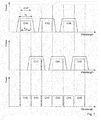
- Fig. 6 shows the optical channel power vs. the wavelength of three adjacent optical channels CH N-1, CH N, CH N+1, wherein, for example, the channels CH N-1 and CH N+1 may be transmitted via the first multiplexer 510 and the channel CH N may be transmitted via the second multiplexer 520.
- the channels comprise a rectangular -shaped or essentially rectangular -shaped spectrum.
- Fig. 6 shows the filter function 610 associated to channel CH N. Said filter function 610 is provided by the optical multiplexer 520 which handles channel CH N.
- the filter function 610 comprises a filter bandwidth wider than the channel bandwidth of the channel CH N.
- the filter bandwidth may be, for example, measured between the points of the filter curve at which the filter curve is 3dB, 1dB or 0.5dB lower than the maximum value of the filter curve, i.e. the filter bandwidth is the 3dB, 1dB or 0.5dB filter bandwidth.
- Using a filter bandwidth larger than the channel bandwidth is advantageous because the side portions of the optical channel are not or essentially not distorted by filtering of the channel leading to a higher system performance.
- By upper-mentioned channel distribution among the at least two multiplexers 510, 520 negative impacts of using optical filters with an filter bandwidth even larger than the channel spacing has no negative impact on adjacent optical channels because said optical channels are transmitted via the further optical multiplexer.
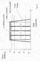
- Fig. 7 shows different schematic spectral channel diagrams, wherein the channel power is plotted against the wavelength.
- the upper spectral channel diagram shows the spectra of the even optical channels CH0, CH 2 and CH4 and the respective filter functions implemented by the first optical multiplexer 510 handling said even optical channels.
- the dotted lines indicate the channel spacing according to the channel grid of the WDM system.
- the channel bandwidth b ch is equal or slightly smaller than the channel spacing ⁇ CH.
- the filter bandwidth b f of the optical filter function used for filtering the respective channels CH0, CH2, CH4 is larger than the channel spacing ⁇ CH.
- the 3dB-bandwitdh of the optical filter may be at least 10 GHz (e.g. 12.5 GHz) wider than the channel width or channel spacing.
- Fig. 7 shows that there is a free gap between two successive channels CH0, CH2 handled by the first optical multiplexer 510. Thereby, the filter function being broader than the channel spacing ⁇ CH has no negative impact on adjacent channels.
- the middle spectral channel diagram of Fig. 7 shows the spectra of the odd optical channels CH1, CH 3and CH5 and the respective filter functions implemented by the second optical multiplexer 520 handling said odd optical channels. Similar to the upper spectral channel diagram, the channel bandwidth b ch is equal or slightly smaller than the channel spacing ⁇ CH. In addition, the filter bandwidth b f of the optical filter function used for filtering the respective channels CH1, CH3, CH5 is larger than the channel spacing ⁇ CH. So, the second optical multiplexer 520 handles every second optical channel, which leads again to gaps between two successive channels, e.g. CH1, CH3 handled by the second optical multiplexer 520 thereby avoiding optical filtering of direct adjacent channels due to the filter function broader then the channel spacing ⁇ CH.
- the last spectral channel diagram of Fig. 7 shows the result of combining the odd and even channels shown in the upper and middle spectral channel diagram. Said combining may be performed by the optical coupler 530.
- the gaps between two channels handled by the first multiplexer 510 are filled by channels handled by the second optical multiplexer 520.
- a plurality of square- or rectangular- shaped channels comprising a channel bandwidth b ch equal or slightly smaller than the channel spacing ⁇ CH are transmitted next to each other, wherein there are no channel distortions at the side portions of the respective channels due to a decreasing of the filter curve.
- Fig. 8 shows a further embodiment of an optical transmission system 800.
- the basic structure of the optical transmission system 800 corresponds to the structure of the optical transmission system 500 shown in Fig. 5 . Therefore, only the differences of the optical transmission system 800 with respect to the optical transmission system 500 are explained. Otherwise, the description of the optical transmission system 500 shall apply accordingly.
- the optical transmission system 800 comprises an optical multiplexing system 800a and an optical demultiplexing system 800b coupled by an optical transmission path 840.
- the optical multiplexing system 800a comprises multiple optical multiplexer, each optical multiplexer implemented by a WSS 810, 820.
- the optical multiplexing system 800a comprises at least one optical coupler 830 for receiving the optical output signals of the WSS 810, 820 and combining said optical signals for transmission via the optical transmission path 840.
- the 1:2 coupler 830 may be replaced by a larger coupler (1:3; 1:4; ).
- the optical demultiplexing system 800b comprises an optical splitter 850 and two or more optical demultiplexer, each optical demultiplexer implemented by a WSS 860, 870.
- the optical signals transmitted via the optical transmission path 840 are splitted by means of the optical splitter 850 in at least two signal portions, each signal portion to be provided to an input of one of the WSS 860, 870.
- the 1:2 splitter 550 may be replaced by a larger splitter (1:3; 1:4; ).
- the WSS 860, 870 are adapted to demultiplex single optical channels or groups of optical channels in order to provide said demultiplexed optical channels to the output of the WSS 860, 870.
- the outputs of the WSS 860, 870 may be coupled with optical receivers, in particular coherent optical receivers for converting the optical signals into the electrical domain. Similar to the multiplexing part, 1:4 optical couplers/splitters (similar to the ones of the multiplexing part) may be added at the outputs of WSS1 and WSS2. This allows coupling with the optical receivers associated with the respective wavelengths of the optical channels.
- the number of inputs 811, 821 of the WSS 810, 820 is limited because of the disproportional increase of complexity of the WSS with increasing number of inputs.
- Typical flexgrid WSS have a limited number of ports, e.g. 20 ports.
- at least one input 811, 821 may be coupled with an optical coupler 880.
- Said optical coupler 880 may comprise a plurality of optical inputs 881, each input e.g. to be coupled with an optical transmitter for receiving on optical signal according to an optical channel of an optical channel grid. Thereby, a number of optical signals associated with different optical channels are combined and provided to a single optical input 810.
- each optical coupler 880 may be adjacent channels of an optical channel grid.
- a limited number of channels typically less than 10, e.g. 2, 3, 4, 5 or 6.
- the number of channels associated with different WSS inputs may vary and not be the same.
- the disadvantage of using optical couplers and having multiple channels associated with one multiplexer input are signal peaks within the channel bandwidth of one optical channel caused by adjacent channels (see Fig. 4 ).
- the signal peaks may be caused, e.g., by imperfections of digital-to-analog converters for generating the optical signals coupled with the optical inputs 881 of optical coupler 880, for example.
- the signal peaks may be caused by aliasing effects or by imperfect interleaving of subDACs of a high speed DAC.
- these effects can be reduced so that the impact is low if DAC sampling speed is increased compared to baudrate, or if the quality of the DAC is improved (e.g. better interleaving of subDACs, and thus better ENOB -effective number of bit- of the DAC).
- the WSS 810, 820 comprise a programmable filter unit for applying a filtering function on the optical channel to be transmitted via the WSS 810, 820.
- the filtering function of each input 811, 821 of WSS 810, 820 may be adapted to the number of optical channels, i.e. at the bandwidth of the set of channels received at each input. More specifically, the filter bandwidth of the filter function applied to the optical signal received at a particular optical input 811, 821 (also called port) may be larger than the summed bandwidth of all channels of the set of channels. In other words, the filter function applied to adjacent optical channel sets may overlap. Thereby, the side slopes of the optical signals at the outer channels of a channel set are not cut off.
- adjacent optical channel sets are alternately distributed across different WSS 810, 820.
- a first channel set and a third channel set e.g. comprising channels 1-4, and channels 9 - 12 are transmitted via the first WSS 810, wherein a second channel set and a fourth channel set, e.g. comprising channels 5 - 8, and channels 13 - 16, are transmitted via the second WSS 820.
- Said channel set distribution is advantageous, because the filter bandwidth of the filter functions for filtering the channel sets can be broader than the bandwidth of the set of channels to be transmitted, wherein the filter functions provided by each WSS do not overlap.
- the filter bandwidth of the filter functions should be larger than the total bandwidth of the N associated channels (or N times the channel spacing) to avoid cutting off the spectrum of optical channels by filtering in the (de)multiplexer or WSS.
- the filter bandwidth should not extend unnecessary beyond the channel bandwidths to avoid that noise (e.g. from ASE) from outside the channels is included for transmission via the optical transmission path 840, thereby reducing OSNR. This will be explained in more detail with reference to Fig. 10 below.
- the optical signals transmitted via the optical transmission path 840 are splitted by means of the optical splitter 850 in at least two signal portions. Each signal portion comprises the whole wavelength spectrum, i.e. all optical channels transmitted via the optical transmission path 840.
- the WSS 860, 870 are adapted to demultiplex single optical channels or groups of optical channels out of the signal portions for providing demultiplexed optical channels or groups of optical channels at the output of the WSS 860, 870.
- the adjacent optical channels or adjacent optical channel sets are demultiplexed alternately at different WSS 860, 870, i.e.
- a first optical channel/first set of optical channels is demultiplexed at a first WSS 860, wherein the second optical channel/second set of optical channels adjacent to the first optical channel/first set of optical channels is demultiplexed at a second WSS 870.
- the filter functions provided by the WSS 860, 870 for filtering the adjacent optical channel / sets of optical channels may overlap, as indicated in Fig. 9 .
- the filter bandwidth of the filter function provided by the WSS 860, 870 is larger than the bandwidth of the optical channel / the set of optical channels to be filtered by said filter function.
- a set of channels is provided at each output of a demultiplexer.
- An optical coupler may be used to split the signals at a demultiplexer output port and provide the respective split signal portions to a corresponding number of coherent receivers.
- Each coherent receiver can select a single channel and reject the others by using appropriate signal processing. It is however preferred to provide not all channels to each receiver but use the filter functions in the demultiplexers to make a selection, in order to avoid quality impairments (penalties) when a large number of channels is supplied to a receiver, and to avoid difficulties to correctly manage signal power and to have enough power per channel.
- a channel set with 4 channels is output at each demultiplexer output port, plus a small part of the left channel and a small part of the right channel to the channel set.
- the same spectrum (4 channels + 2 small parts) is provided.
- the coherent receiver coupled with a coupler port can select a single channel and reject the (three) others. As mentioned, it is preferable to supply only a few channels to a coherent receiver, and not the full 80 or 160 channels that are transmitted via the optical transmission path.
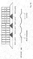
- Fig. 10 illustrates schematically the distribution of signals and noise at the output of the optical coupler 830.
- the figure shows channels 1-16 transmitted by the input ports of MUX1 and MUX2 (WSS1 and WSS2). In the depicted example, each port receives and transmits 4 optical channels.
- Fig. 10 further illustrates schematically the filter functions associated with the input ports of the multiplexers. The overlap of adjacent filter functions is shaded. As already mentioned, the filters not only pass optical channel signals in their passbands but also noise such as caused by ASE. In the areas where the filter functions overlap, the noise adds up, as shown in the lower part of the figure, resulting in a 3dB noise increase in the overlap areas, which may impact the channels at the borders of the filter functions.
- Fig. 10 illustrates schematically the distribution of signals and noise at the output of the optical coupler 830.
- the figure shows channels 1-16 transmitted by the input ports of MUX1 and MUX2 (WSS1 and WSS2). In the depicted example,
- FIG. 10 further marks the slope of the noise bumps and its steepness.
- optical filters with a steepness of ⁇ 5GHz from 1dB to 20dB attenuation may be used.
- the steepness is a property of an optical filter and is defined by a difference in bandwidths of a filter function at different attenuation levels. Please note that the dimensions shown in Fig. 10 are not to scale and are depicted only schematically.
- Fig. 11 illustrates schematically an example optical filter for use in a multiplexer or demultiplexer of an optical transmission system according to embodiments.
- Fig. 10 illustrates the spectral filter shape for the case where 4 optical channels are assigned to one (de)multiplexer input. The figure shows different bandwidths of the filter function, namely the 0.5dB-bandwidth where the power of a filtered signal is attenuated by 0.5dB, the 1dB-bandwidth where the power of a filtered signal is attenuated by 1dB, etc.
- the following filter parameters may be used: a 0.5dB-bandwidth of 203GHz; a 1dB-bandwidth of 206GHz; a 3dB-bandwidth of 210GHz; a 10dB-bandwidth of 213GHz; and a 20dB-bandwidth of 216GHz.
- the "steepness" of the filter between 1dB and 20dB would be 5GHz on each side (i.e. 10GHz in total corresponding to the difference between the above 20dB-bandwidth and the 1dB-bandwidth: 216-206GHz).
- a small overlap (4GHz for example) of the filter functions at 0dB or 1dB attenuation may be employed to ensure no filtering of the channels even taking into account some uncertainties in the filters.
- the choice of the "overlap at 1dB” may be linked to the accuracy of the filter position. If there is an accuracy of +/-2GHz for each filter, the overlap at 1dB should be 4GHz.
- the "overlap at 20dB" is then equal to the "overlap at 1dB + twice the steepness" (if the steepness is defined as the difference of frequency between 1dB attenuation and 20dB attenuation as mentioned above).
- any block diagrams herein represent conceptual views of illustrative circuitry embodying the principles of the invention.
- any flow charts, flow diagrams, state transition diagrams, pseudo code, and the like represent various processes which may be substantially represented in computer readable medium and so executed by a computer or processor, whether or not such computer or processor is explicitly shown.
- processor or “computer” should not be construed to refer exclusively to hardware capable of executing software, and may implicitly include, without limitation, digital signal processor (DSP) hardware, network processor, application specific integrated circuit (ASIC), field programmable gate array (FPGA), read-only memory (ROM) for storing software, random-access memory (RAM), and non-volatile storage.
- DSP digital signal processor
- ASIC application specific integrated circuit
- FPGA field programmable gate array
- ROM read-only memory
- RAM random-access memory
- non-volatile storage Other hardware, conventional and/or custom, may also be included.
Landscapes
- Engineering & Computer Science (AREA)
- Computer Networks & Wireless Communication (AREA)
- Signal Processing (AREA)
- Optical Communication System (AREA)
Priority Applications (2)
| Application Number | Priority Date | Filing Date | Title |
|---|---|---|---|
| EP14305343.7A EP2919404B1 (de) | 2014-03-10 | 2014-03-10 | Multiplexsystem und System zum Demultiplexen für WDM-Kanalübertragung |
| PCT/EP2015/052132 WO2015135695A1 (en) | 2014-03-10 | 2015-02-03 | Multiplexing system and demultiplexing system for wdm channel transmission |
Applications Claiming Priority (1)
| Application Number | Priority Date | Filing Date | Title |
|---|---|---|---|
| EP14305343.7A EP2919404B1 (de) | 2014-03-10 | 2014-03-10 | Multiplexsystem und System zum Demultiplexen für WDM-Kanalübertragung |
Publications (2)
| Publication Number | Publication Date |
|---|---|
| EP2919404A1 true EP2919404A1 (de) | 2015-09-16 |
| EP2919404B1 EP2919404B1 (de) | 2016-07-20 |
Family
ID=50391120
Family Applications (1)
| Application Number | Title | Priority Date | Filing Date |
|---|---|---|---|
| EP14305343.7A Active EP2919404B1 (de) | 2014-03-10 | 2014-03-10 | Multiplexsystem und System zum Demultiplexen für WDM-Kanalübertragung |
Country Status (2)
| Country | Link |
|---|---|
| EP (1) | EP2919404B1 (de) |
| WO (1) | WO2015135695A1 (de) |
Cited By (3)
| Publication number | Priority date | Publication date | Assignee | Title |
|---|---|---|---|---|
| CN110892656A (zh) * | 2017-07-28 | 2020-03-17 | 日本电气株式会社 | 光波长分离装置及光波长分离方法 |
| CN114944882A (zh) * | 2022-05-16 | 2022-08-26 | 烽火通信科技股份有限公司 | 一种非固定波道间隔混传下的切波方法及系统 |
| EP4344104A1 (de) * | 2022-09-20 | 2024-03-27 | Adtran Networks SE | Netzknoten für ein kohärentes optisches wdm-übertragungsnetzwerk |
Families Citing this family (1)
| Publication number | Priority date | Publication date | Assignee | Title |
|---|---|---|---|---|
| CN115314782B (zh) * | 2022-08-26 | 2024-11-12 | 烽火通信科技股份有限公司 | 一种信道填充方法和装置 |
Citations (5)
| Publication number | Priority date | Publication date | Assignee | Title |
|---|---|---|---|---|
| WO2001019007A1 (en) * | 1999-09-08 | 2001-03-15 | Chorum Technologies Lp | Apparatus for wavelength demultiplexing using a multi-cavity etalon |
| WO2002054642A2 (en) * | 2000-12-29 | 2002-07-11 | Luxcore Networks, Inc. | High density reconfigurable optical multiplexer |
| US20090022618A1 (en) * | 2006-02-21 | 2009-01-22 | Jfe Steel Corporation | Damping Alloy Steel Sheet and Method for Producing the Same |
| WO2011113679A1 (en) * | 2010-03-18 | 2011-09-22 | Alcatel Lucent | Method for optimizing the capacity of optical communication networks |
| WO2012163301A1 (en) * | 2011-06-03 | 2012-12-06 | Huawei Technologies Co., Ltd. | Method and apparatus for colorless add |
-
2014
- 2014-03-10 EP EP14305343.7A patent/EP2919404B1/de active Active
-
2015
- 2015-02-03 WO PCT/EP2015/052132 patent/WO2015135695A1/en not_active Ceased
Patent Citations (5)
| Publication number | Priority date | Publication date | Assignee | Title |
|---|---|---|---|---|
| WO2001019007A1 (en) * | 1999-09-08 | 2001-03-15 | Chorum Technologies Lp | Apparatus for wavelength demultiplexing using a multi-cavity etalon |
| WO2002054642A2 (en) * | 2000-12-29 | 2002-07-11 | Luxcore Networks, Inc. | High density reconfigurable optical multiplexer |
| US20090022618A1 (en) * | 2006-02-21 | 2009-01-22 | Jfe Steel Corporation | Damping Alloy Steel Sheet and Method for Producing the Same |
| WO2011113679A1 (en) * | 2010-03-18 | 2011-09-22 | Alcatel Lucent | Method for optimizing the capacity of optical communication networks |
| WO2012163301A1 (en) * | 2011-06-03 | 2012-12-06 | Huawei Technologies Co., Ltd. | Method and apparatus for colorless add |
Cited By (6)
| Publication number | Priority date | Publication date | Assignee | Title |
|---|---|---|---|---|
| CN110892656A (zh) * | 2017-07-28 | 2020-03-17 | 日本电气株式会社 | 光波长分离装置及光波长分离方法 |
| JPWO2019021972A1 (ja) * | 2017-07-28 | 2020-04-16 | 日本電気株式会社 | 光波長分離装置及び光波長分離方法 |
| EP3661083A4 (de) * | 2017-07-28 | 2020-09-02 | Nec Corporation | Lichtwellenlängentrennvorrichtung und lichtwellenlängentrennverfahren |
| CN114944882A (zh) * | 2022-05-16 | 2022-08-26 | 烽火通信科技股份有限公司 | 一种非固定波道间隔混传下的切波方法及系统 |
| EP4344104A1 (de) * | 2022-09-20 | 2024-03-27 | Adtran Networks SE | Netzknoten für ein kohärentes optisches wdm-übertragungsnetzwerk |
| US12542612B2 (en) | 2022-09-20 | 2026-02-03 | Adtran Networks Se | Network node for a coherent optical WDM transmission network |
Also Published As
| Publication number | Publication date |
|---|---|
| EP2919404B1 (de) | 2016-07-20 |
| WO2015135695A1 (en) | 2015-09-17 |
Similar Documents
| Publication | Publication Date | Title |
|---|---|---|
| US10200145B2 (en) | Flexible grid optical spectrum transmitter, receiver, and transceiver | |
| KR101449977B1 (ko) | 광 통신 네트워크들의 용량을 최적화하기 위한 방법 | |
| JP4588234B2 (ja) | 光デバイス及びこれを用いる波長多重通信システム | |
| US8958695B2 (en) | Optical adding and dropping device and optical transmission apparatus | |
| EP1088417B1 (de) | Verfahren und vorrichtung zur abzweigung von optischen kanälen in einem optischen übertragungssystem | |
| US20010024542A1 (en) | Method and device for dropping optical channels in an optical transmission system | |
| JP5807338B2 (ja) | 光伝送装置および光フィルタ回路 | |
| EP2919404B1 (de) | Multiplexsystem und System zum Demultiplexen für WDM-Kanalübertragung | |
| EP3189603B1 (de) | Laden optischer leitungen mit variablem bandbreitenrauschen | |
| JP4002063B2 (ja) | 光波長分岐/挿入マルチプレクサ及びそれに使用されるフィルタ要素 | |
| EP1261160A2 (de) | Optischer Add/Drop Multiplexer | |
| JP2002296629A (ja) | 4光波混合を用い雑音を考慮した波長変換方法と波長変換器および光源 | |
| EP1461886B1 (de) | Rauschminderung in optischen kommunikationsnetzwerken | |
| US8849113B2 (en) | Wavelength selective switch and optical transmission apparatus | |
| Pan et al. | Filtering and crosstalk penalties for PDM-8QAM/16QAM super-channels in DWDM networks using broadcast-and-select and route-and-select ROADMs | |
| JPWO2019021972A1 (ja) | 光波長分離装置及び光波長分離方法 | |
| JP4819107B2 (ja) | 光伝送装置 | |
| EP2134007B1 (de) | Verfahren und Geräte zur Verringerung von Übersprechen in optischen Netzwerken | |
| JP3058265B2 (ja) | 波長多重光伝送システムに用いる光合分波装置 | |
| US20230327795A1 (en) | Intra-carrier spectral shaping for high-baud rate optical transmission signals | |
| Takashina et al. | Low crosstalk wavelength tunable filter that utilizes symmetric and asymmetric Mach-Zehnder interferometers | |
| CN119675817A (zh) | 部分彩色灵活栅格波分复用器/解复用器 | |
| Ji et al. | Reconfigurable waveband cross-connect and its application in 112 Gb/s WDM system | |
| EP2838211A1 (de) | Filterung eines optischen WDM-Signals mit einem Konfigurationsfilter |
Legal Events
| Date | Code | Title | Description |
|---|---|---|---|
| PUAI | Public reference made under article 153(3) epc to a published international application that has entered the european phase |
Free format text: ORIGINAL CODE: 0009012 |
|
| 17P | Request for examination filed |
Effective date: 20141010 |
|
| AK | Designated contracting states |
Kind code of ref document: A1 Designated state(s): AL AT BE BG CH CY CZ DE DK EE ES FI FR GB GR HR HU IE IS IT LI LT LU LV MC MK MT NL NO PL PT RO RS SE SI SK SM TR |
|
| AX | Request for extension of the european patent |
Extension state: BA ME |
|
| GRAP | Despatch of communication of intention to grant a patent |
Free format text: ORIGINAL CODE: EPIDOSNIGR1 |
|
| INTG | Intention to grant announced |
Effective date: 20160401 |
|
| RBV | Designated contracting states (corrected) |
Designated state(s): AL AT BE BG CH CY CZ DE DK EE ES FI FR GB GR HR HU IE IS IT LI LT LU LV MC MK MT NL NO PL PT RO RS SE SI SK SM TR |
|
| GRAS | Grant fee paid |
Free format text: ORIGINAL CODE: EPIDOSNIGR3 |
|
| GRAA | (expected) grant |
Free format text: ORIGINAL CODE: 0009210 |
|
| AK | Designated contracting states |
Kind code of ref document: B1 Designated state(s): AL AT BE BG CH CY CZ DE DK EE ES FI FR GB GR HR HU IE IS IT LI LT LU LV MC MK MT NL NO PL PT RO RS SE SI SK SM TR |
|
| REG | Reference to a national code |
Ref country code: GB Ref legal event code: FG4D |
|
| REG | Reference to a national code |
Ref country code: CH Ref legal event code: EP |
|
| REG | Reference to a national code |
Ref country code: IE Ref legal event code: FG4D |
|
| REG | Reference to a national code |
Ref country code: AT Ref legal event code: REF Ref document number: 814833 Country of ref document: AT Kind code of ref document: T Effective date: 20160815 |
|
| REG | Reference to a national code |
Ref country code: DE Ref legal event code: R096 Ref document number: 602014002776 Country of ref document: DE |
|
| REG | Reference to a national code |
Ref country code: LT Ref legal event code: MG4D |
|
| REG | Reference to a national code |
Ref country code: NL Ref legal event code: MP Effective date: 20160720 |
|
| REG | Reference to a national code |
Ref country code: AT Ref legal event code: MK05 Ref document number: 814833 Country of ref document: AT Kind code of ref document: T Effective date: 20160720 |
|
| PG25 | Lapsed in a contracting state [announced via postgrant information from national office to epo] |
Ref country code: NO Free format text: LAPSE BECAUSE OF FAILURE TO SUBMIT A TRANSLATION OF THE DESCRIPTION OR TO PAY THE FEE WITHIN THE PRESCRIBED TIME-LIMIT Effective date: 20161020 Ref country code: IT Free format text: LAPSE BECAUSE OF FAILURE TO SUBMIT A TRANSLATION OF THE DESCRIPTION OR TO PAY THE FEE WITHIN THE PRESCRIBED TIME-LIMIT Effective date: 20160720 Ref country code: FI Free format text: LAPSE BECAUSE OF FAILURE TO SUBMIT A TRANSLATION OF THE DESCRIPTION OR TO PAY THE FEE WITHIN THE PRESCRIBED TIME-LIMIT Effective date: 20160720 Ref country code: RS Free format text: LAPSE BECAUSE OF FAILURE TO SUBMIT A TRANSLATION OF THE DESCRIPTION OR TO PAY THE FEE WITHIN THE PRESCRIBED TIME-LIMIT Effective date: 20160720 Ref country code: IS Free format text: LAPSE BECAUSE OF FAILURE TO SUBMIT A TRANSLATION OF THE DESCRIPTION OR TO PAY THE FEE WITHIN THE PRESCRIBED TIME-LIMIT Effective date: 20161120 Ref country code: NL Free format text: LAPSE BECAUSE OF FAILURE TO SUBMIT A TRANSLATION OF THE DESCRIPTION OR TO PAY THE FEE WITHIN THE PRESCRIBED TIME-LIMIT Effective date: 20160720 Ref country code: HR Free format text: LAPSE BECAUSE OF FAILURE TO SUBMIT A TRANSLATION OF THE DESCRIPTION OR TO PAY THE FEE WITHIN THE PRESCRIBED TIME-LIMIT Effective date: 20160720 Ref country code: LT Free format text: LAPSE BECAUSE OF FAILURE TO SUBMIT A TRANSLATION OF THE DESCRIPTION OR TO PAY THE FEE WITHIN THE PRESCRIBED TIME-LIMIT Effective date: 20160720 |
|
| PG25 | Lapsed in a contracting state [announced via postgrant information from national office to epo] |
Ref country code: BE Free format text: LAPSE BECAUSE OF FAILURE TO SUBMIT A TRANSLATION OF THE DESCRIPTION OR TO PAY THE FEE WITHIN THE PRESCRIBED TIME-LIMIT Effective date: 20160720 Ref country code: PL Free format text: LAPSE BECAUSE OF FAILURE TO SUBMIT A TRANSLATION OF THE DESCRIPTION OR TO PAY THE FEE WITHIN THE PRESCRIBED TIME-LIMIT Effective date: 20160720 Ref country code: GR Free format text: LAPSE BECAUSE OF FAILURE TO SUBMIT A TRANSLATION OF THE DESCRIPTION OR TO PAY THE FEE WITHIN THE PRESCRIBED TIME-LIMIT Effective date: 20161021 Ref country code: AT Free format text: LAPSE BECAUSE OF FAILURE TO SUBMIT A TRANSLATION OF THE DESCRIPTION OR TO PAY THE FEE WITHIN THE PRESCRIBED TIME-LIMIT Effective date: 20160720 Ref country code: ES Free format text: LAPSE BECAUSE OF FAILURE TO SUBMIT A TRANSLATION OF THE DESCRIPTION OR TO PAY THE FEE WITHIN THE PRESCRIBED TIME-LIMIT Effective date: 20160720 Ref country code: SE Free format text: LAPSE BECAUSE OF FAILURE TO SUBMIT A TRANSLATION OF THE DESCRIPTION OR TO PAY THE FEE WITHIN THE PRESCRIBED TIME-LIMIT Effective date: 20160720 Ref country code: PT Free format text: LAPSE BECAUSE OF FAILURE TO SUBMIT A TRANSLATION OF THE DESCRIPTION OR TO PAY THE FEE WITHIN THE PRESCRIBED TIME-LIMIT Effective date: 20161121 Ref country code: LV Free format text: LAPSE BECAUSE OF FAILURE TO SUBMIT A TRANSLATION OF THE DESCRIPTION OR TO PAY THE FEE WITHIN THE PRESCRIBED TIME-LIMIT Effective date: 20160720 |
|
| REG | Reference to a national code |
Ref country code: FR Ref legal event code: PLFP Year of fee payment: 4 |
|
| REG | Reference to a national code |
Ref country code: DE Ref legal event code: R097 Ref document number: 602014002776 Country of ref document: DE |
|
| PG25 | Lapsed in a contracting state [announced via postgrant information from national office to epo] |
Ref country code: RO Free format text: LAPSE BECAUSE OF FAILURE TO SUBMIT A TRANSLATION OF THE DESCRIPTION OR TO PAY THE FEE WITHIN THE PRESCRIBED TIME-LIMIT Effective date: 20160720 Ref country code: EE Free format text: LAPSE BECAUSE OF FAILURE TO SUBMIT A TRANSLATION OF THE DESCRIPTION OR TO PAY THE FEE WITHIN THE PRESCRIBED TIME-LIMIT Effective date: 20160720 |
|
| PLBE | No opposition filed within time limit |
Free format text: ORIGINAL CODE: 0009261 |
|
| STAA | Information on the status of an ep patent application or granted ep patent |
Free format text: STATUS: NO OPPOSITION FILED WITHIN TIME LIMIT |
|
| PG25 | Lapsed in a contracting state [announced via postgrant information from national office to epo] |
Ref country code: CZ Free format text: LAPSE BECAUSE OF FAILURE TO SUBMIT A TRANSLATION OF THE DESCRIPTION OR TO PAY THE FEE WITHIN THE PRESCRIBED TIME-LIMIT Effective date: 20160720 Ref country code: BG Free format text: LAPSE BECAUSE OF FAILURE TO SUBMIT A TRANSLATION OF THE DESCRIPTION OR TO PAY THE FEE WITHIN THE PRESCRIBED TIME-LIMIT Effective date: 20161020 Ref country code: SM Free format text: LAPSE BECAUSE OF FAILURE TO SUBMIT A TRANSLATION OF THE DESCRIPTION OR TO PAY THE FEE WITHIN THE PRESCRIBED TIME-LIMIT Effective date: 20160720 Ref country code: SK Free format text: LAPSE BECAUSE OF FAILURE TO SUBMIT A TRANSLATION OF THE DESCRIPTION OR TO PAY THE FEE WITHIN THE PRESCRIBED TIME-LIMIT Effective date: 20160720 Ref country code: DK Free format text: LAPSE BECAUSE OF FAILURE TO SUBMIT A TRANSLATION OF THE DESCRIPTION OR TO PAY THE FEE WITHIN THE PRESCRIBED TIME-LIMIT Effective date: 20160720 |
|
| 26N | No opposition filed |
Effective date: 20170421 |
|
| PG25 | Lapsed in a contracting state [announced via postgrant information from national office to epo] |
Ref country code: SI Free format text: LAPSE BECAUSE OF FAILURE TO SUBMIT A TRANSLATION OF THE DESCRIPTION OR TO PAY THE FEE WITHIN THE PRESCRIBED TIME-LIMIT Effective date: 20160720 |
|
| REG | Reference to a national code |
Ref country code: CH Ref legal event code: PL |
|
| PG25 | Lapsed in a contracting state [announced via postgrant information from national office to epo] |
Ref country code: MC Free format text: LAPSE BECAUSE OF FAILURE TO SUBMIT A TRANSLATION OF THE DESCRIPTION OR TO PAY THE FEE WITHIN THE PRESCRIBED TIME-LIMIT Effective date: 20160720 |
|
| REG | Reference to a national code |
Ref country code: IE Ref legal event code: MM4A |
|
| PG25 | Lapsed in a contracting state [announced via postgrant information from national office to epo] |
Ref country code: LU Free format text: LAPSE BECAUSE OF NON-PAYMENT OF DUE FEES Effective date: 20170310 |
|
| PG25 | Lapsed in a contracting state [announced via postgrant information from national office to epo] |
Ref country code: LI Free format text: LAPSE BECAUSE OF NON-PAYMENT OF DUE FEES Effective date: 20170331 Ref country code: IE Free format text: LAPSE BECAUSE OF NON-PAYMENT OF DUE FEES Effective date: 20170310 Ref country code: CH Free format text: LAPSE BECAUSE OF NON-PAYMENT OF DUE FEES Effective date: 20170331 |
|
| REG | Reference to a national code |
Ref country code: FR Ref legal event code: PLFP Year of fee payment: 5 |
|
| PG25 | Lapsed in a contracting state [announced via postgrant information from national office to epo] |
Ref country code: MT Free format text: LAPSE BECAUSE OF NON-PAYMENT OF DUE FEES Effective date: 20170310 |
|
| PG25 | Lapsed in a contracting state [announced via postgrant information from national office to epo] |
Ref country code: AL Free format text: LAPSE BECAUSE OF FAILURE TO SUBMIT A TRANSLATION OF THE DESCRIPTION OR TO PAY THE FEE WITHIN THE PRESCRIBED TIME-LIMIT Effective date: 20160720 |
|
| PG25 | Lapsed in a contracting state [announced via postgrant information from national office to epo] |
Ref country code: HU Free format text: LAPSE BECAUSE OF FAILURE TO SUBMIT A TRANSLATION OF THE DESCRIPTION OR TO PAY THE FEE WITHIN THE PRESCRIBED TIME-LIMIT; INVALID AB INITIO Effective date: 20140310 |
|
| PG25 | Lapsed in a contracting state [announced via postgrant information from national office to epo] |
Ref country code: CY Free format text: LAPSE BECAUSE OF FAILURE TO SUBMIT A TRANSLATION OF THE DESCRIPTION OR TO PAY THE FEE WITHIN THE PRESCRIBED TIME-LIMIT Effective date: 20160720 |
|
| PG25 | Lapsed in a contracting state [announced via postgrant information from national office to epo] |
Ref country code: MK Free format text: LAPSE BECAUSE OF FAILURE TO SUBMIT A TRANSLATION OF THE DESCRIPTION OR TO PAY THE FEE WITHIN THE PRESCRIBED TIME-LIMIT Effective date: 20160720 |
|
| PG25 | Lapsed in a contracting state [announced via postgrant information from national office to epo] |
Ref country code: TR Free format text: LAPSE BECAUSE OF FAILURE TO SUBMIT A TRANSLATION OF THE DESCRIPTION OR TO PAY THE FEE WITHIN THE PRESCRIBED TIME-LIMIT Effective date: 20160720 |
|
| PGFP | Annual fee paid to national office [announced via postgrant information from national office to epo] |
Ref country code: FR Payment date: 20200214 Year of fee payment: 7 |
|
| PG25 | Lapsed in a contracting state [announced via postgrant information from national office to epo] |
Ref country code: FR Free format text: LAPSE BECAUSE OF NON-PAYMENT OF DUE FEES Effective date: 20210331 |
|
| PGFP | Annual fee paid to national office [announced via postgrant information from national office to epo] |
Ref country code: GB Payment date: 20260202 Year of fee payment: 13 |
|
| PGFP | Annual fee paid to national office [announced via postgrant information from national office to epo] |
Ref country code: DE Payment date: 20260204 Year of fee payment: 13 |