EP2920009B1 - One up, one down connection structure for piezoelectric device in tire patch - Google Patents
One up, one down connection structure for piezoelectric device in tire patch Download PDFInfo
- Publication number
- EP2920009B1 EP2920009B1 EP12888379.0A EP12888379A EP2920009B1 EP 2920009 B1 EP2920009 B1 EP 2920009B1 EP 12888379 A EP12888379 A EP 12888379A EP 2920009 B1 EP2920009 B1 EP 2920009B1
- Authority
- EP
- European Patent Office
- Prior art keywords
- conductive
- insulating layer
- substrate
- conductive terminal
- layer
- Prior art date
- Legal status (The legal status is an assumption and is not a legal conclusion. Google has not performed a legal analysis and makes no representation as to the accuracy of the status listed.)
- Active
Links
Images



Classifications
-
- B—PERFORMING OPERATIONS; TRANSPORTING
- B60—VEHICLES IN GENERAL
- B60C—VEHICLE TYRES; TYRE INFLATION; TYRE CHANGING; CONNECTING VALVES TO INFLATABLE ELASTIC BODIES IN GENERAL; DEVICES OR ARRANGEMENTS RELATED TO TYRES
- B60C23/00—Devices for measuring, signalling, controlling, or distributing tyre pressure or temperature, specially adapted for mounting on vehicles; Arrangement of tyre inflating devices on vehicles, e.g. of pumps or of tanks; Tyre cooling arrangements
- B60C23/02—Signalling devices actuated by tyre pressure
- B60C23/04—Signalling devices actuated by tyre pressure mounted on the wheel or tyre
- B60C23/0408—Signalling devices actuated by tyre pressure mounted on the wheel or tyre transmitting the signals by non-mechanical means from the wheel or tyre to a vehicle body mounted receiver
- B60C23/041—Means for supplying power to the signal- transmitting means on the wheel
- B60C23/0411—Piezoelectric generators
-
- H—ELECTRICITY
- H10—SEMICONDUCTOR DEVICES; ELECTRIC SOLID-STATE DEVICES NOT OTHERWISE PROVIDED FOR
- H10N—ELECTRIC SOLID-STATE DEVICES NOT OTHERWISE PROVIDED FOR
- H10N30/00—Piezoelectric or electrostrictive devices
- H10N30/80—Constructional details
- H10N30/87—Electrodes or interconnections, e.g. leads or terminals
-
- B—PERFORMING OPERATIONS; TRANSPORTING
- B23—MACHINE TOOLS; METAL-WORKING NOT OTHERWISE PROVIDED FOR
- B23K—SOLDERING OR UNSOLDERING; WELDING; CLADDING OR PLATING BY SOLDERING OR WELDING; CUTTING BY APPLYING HEAT LOCALLY, e.g. FLAME CUTTING; WORKING BY LASER BEAM
- B23K1/00—Soldering, e.g. brazing, or unsoldering
- B23K1/0008—Soldering, e.g. brazing, or unsoldering specially adapted for particular articles or work
- B23K1/0016—Soldering of electronic components
-
- B—PERFORMING OPERATIONS; TRANSPORTING
- B23—MACHINE TOOLS; METAL-WORKING NOT OTHERWISE PROVIDED FOR
- B23K—SOLDERING OR UNSOLDERING; WELDING; CLADDING OR PLATING BY SOLDERING OR WELDING; CUTTING BY APPLYING HEAT LOCALLY, e.g. FLAME CUTTING; WORKING BY LASER BEAM
- B23K31/00—Processes relevant to this subclass, specially adapted for particular articles or purposes, but not covered by any single one of main groups B23K1/00 - B23K28/00
- B23K31/02—Processes relevant to this subclass, specially adapted for particular articles or purposes, but not covered by any single one of main groups B23K1/00 - B23K28/00 relating to soldering or welding
-
- B—PERFORMING OPERATIONS; TRANSPORTING
- B29—WORKING OF PLASTICS; WORKING OF SUBSTANCES IN A PLASTIC STATE IN GENERAL
- B29C—SHAPING OR JOINING OF PLASTICS; SHAPING OF MATERIAL IN A PLASTIC STATE, NOT OTHERWISE PROVIDED FOR; AFTER-TREATMENT OF THE SHAPED PRODUCTS, e.g. REPAIRING
- B29C73/00—Repairing of articles made from plastics or substances in a plastic state, e.g. of articles shaped or produced by using techniques covered by this subclass or subclass B29D
- B29C73/04—Repairing of articles made from plastics or substances in a plastic state, e.g. of articles shaped or produced by using techniques covered by this subclass or subclass B29D using preformed elements
- B29C73/10—Repairing of articles made from plastics or substances in a plastic state, e.g. of articles shaped or produced by using techniques covered by this subclass or subclass B29D using preformed elements using patches sealing on the surface of the article
-
- B—PERFORMING OPERATIONS; TRANSPORTING
- B60—VEHICLES IN GENERAL
- B60C—VEHICLE TYRES; TYRE INFLATION; TYRE CHANGING; CONNECTING VALVES TO INFLATABLE ELASTIC BODIES IN GENERAL; DEVICES OR ARRANGEMENTS RELATED TO TYRES
- B60C19/00—Tyre parts or constructions not otherwise provided for
-
- B—PERFORMING OPERATIONS; TRANSPORTING
- B60—VEHICLES IN GENERAL
- B60C—VEHICLE TYRES; TYRE INFLATION; TYRE CHANGING; CONNECTING VALVES TO INFLATABLE ELASTIC BODIES IN GENERAL; DEVICES OR ARRANGEMENTS RELATED TO TYRES
- B60C23/00—Devices for measuring, signalling, controlling, or distributing tyre pressure or temperature, specially adapted for mounting on vehicles; Arrangement of tyre inflating devices on vehicles, e.g. of pumps or of tanks; Tyre cooling arrangements
- B60C23/02—Signalling devices actuated by tyre pressure
- B60C23/04—Signalling devices actuated by tyre pressure mounted on the wheel or tyre
- B60C23/0491—Constructional details of means for attaching the control device
- B60C23/0493—Constructional details of means for attaching the control device for attachment on the tyre
-
- B—PERFORMING OPERATIONS; TRANSPORTING
- B60—VEHICLES IN GENERAL
- B60C—VEHICLE TYRES; TYRE INFLATION; TYRE CHANGING; CONNECTING VALVES TO INFLATABLE ELASTIC BODIES IN GENERAL; DEVICES OR ARRANGEMENTS RELATED TO TYRES
- B60C99/00—Subject matter not provided for in other groups of this subclass
-
- H—ELECTRICITY
- H05—ELECTRIC TECHNIQUES NOT OTHERWISE PROVIDED FOR
- H05K—PRINTED CIRCUITS; CASINGS OR CONSTRUCTIONAL DETAILS OF ELECTRIC APPARATUS; MANUFACTURE OF ASSEMBLAGES OF ELECTRICAL COMPONENTS
- H05K1/00—Printed circuits
- H05K1/18—Printed circuits structurally associated with non-printed electric components
-
- H—ELECTRICITY
- H05—ELECTRIC TECHNIQUES NOT OTHERWISE PROVIDED FOR
- H05K—PRINTED CIRCUITS; CASINGS OR CONSTRUCTIONAL DETAILS OF ELECTRIC APPARATUS; MANUFACTURE OF ASSEMBLAGES OF ELECTRICAL COMPONENTS
- H05K3/00—Apparatus or processes for manufacturing printed circuits
- H05K3/30—Assembling printed circuits with electric components, e.g. with resistors
- H05K3/32—Assembling printed circuits with electric components, e.g. with resistors electrically connecting electric components or wires to printed circuits
- H05K3/34—Assembling printed circuits with electric components, e.g. with resistors electrically connecting electric components or wires to printed circuits by soldering
-
- B—PERFORMING OPERATIONS; TRANSPORTING
- B29—WORKING OF PLASTICS; WORKING OF SUBSTANCES IN A PLASTIC STATE IN GENERAL
- B29L—INDEXING SCHEME ASSOCIATED WITH SUBCLASS B29C, RELATING TO PARTICULAR ARTICLES
- B29L2030/00—Pneumatic or solid tyres or parts thereof
-
- H—ELECTRICITY
- H05—ELECTRIC TECHNIQUES NOT OTHERWISE PROVIDED FOR
- H05K—PRINTED CIRCUITS; CASINGS OR CONSTRUCTIONAL DETAILS OF ELECTRIC APPARATUS; MANUFACTURE OF ASSEMBLAGES OF ELECTRICAL COMPONENTS
- H05K2203/00—Indexing scheme relating to apparatus or processes for manufacturing printed circuits covered by H05K3/00
- H05K2203/04—Soldering or other types of metallurgic bonding
-
- H—ELECTRICITY
- H05—ELECTRIC TECHNIQUES NOT OTHERWISE PROVIDED FOR
- H05K—PRINTED CIRCUITS; CASINGS OR CONSTRUCTIONAL DETAILS OF ELECTRIC APPARATUS; MANUFACTURE OF ASSEMBLAGES OF ELECTRICAL COMPONENTS
- H05K2203/00—Indexing scheme relating to apparatus or processes for manufacturing printed circuits covered by H05K3/00
- H05K2203/11—Treatments characterised by their effect, e.g. heating, cooling, roughening
- H05K2203/1194—Thermal treatment leading to a different chemical state of a material, e.g. annealing for stress-relief, aging
-
- H—ELECTRICITY
- H10—SEMICONDUCTOR DEVICES; ELECTRIC SOLID-STATE DEVICES NOT OTHERWISE PROVIDED FOR
- H10N—ELECTRIC SOLID-STATE DEVICES NOT OTHERWISE PROVIDED FOR
- H10N30/00—Piezoelectric or electrostrictive devices
- H10N30/01—Manufacture or treatment
- H10N30/06—Forming electrodes or interconnections, e.g. leads or terminals
- H10N30/063—Forming interconnections, e.g. connection electrodes of multilayered piezoelectric or electrostrictive parts
-
- H—ELECTRICITY
- H10—SEMICONDUCTOR DEVICES; ELECTRIC SOLID-STATE DEVICES NOT OTHERWISE PROVIDED FOR
- H10N—ELECTRIC SOLID-STATE DEVICES NOT OTHERWISE PROVIDED FOR
- H10N30/00—Piezoelectric or electrostrictive devices
- H10N30/01—Manufacture or treatment
- H10N30/07—Forming of piezoelectric or electrostrictive parts or bodies on an electrical element or another base
- H10N30/072—Forming of piezoelectric or electrostrictive parts or bodies on an electrical element or another base by laminating or bonding of piezoelectric or electrostrictive bodies
- H10N30/073—Forming of piezoelectric or electrostrictive parts or bodies on an electrical element or another base by laminating or bonding of piezoelectric or electrostrictive bodies by fusion of metals or by adhesives
-
- Y—GENERAL TAGGING OF NEW TECHNOLOGICAL DEVELOPMENTS; GENERAL TAGGING OF CROSS-SECTIONAL TECHNOLOGIES SPANNING OVER SEVERAL SECTIONS OF THE IPC; TECHNICAL SUBJECTS COVERED BY FORMER USPC CROSS-REFERENCE ART COLLECTIONS [XRACs] AND DIGESTS
- Y10—TECHNICAL SUBJECTS COVERED BY FORMER USPC
- Y10T—TECHNICAL SUBJECTS COVERED BY FORMER US CLASSIFICATION
- Y10T29/00—Metal working
- Y10T29/42—Piezoelectric device making
Definitions
- the present disclosure relates generally to a piezoelectric device for use as part of a tire patch, and more particularly to an electrical connection structure for a piezoelectric device used as part of a tire patch.
- the document US 2011/132649 A1 is an example of prior art, accordingly to the preamble of claim 1.
- Piezoelectric devices have been incorporated with tire patches to provide a power source to various sensors and other components of a tire patch used to measure tire parameters. Piezoelectric devices have also been used to acquire data about various physical parameters of a tire during rotation of the tire. Such information may be useful in tire monitoring and warning systems as well as in tire testing and design.
- One known structure for a piezoelectric device includes a substrate having one or more piezoelectric components, such as a power generation component and a signal generation component.
- Each piezoelectric component can include a sandwich structure that includes a top conductive layer and a lower conductive layer that sandwich a piezoelectric layer.
- the substrate can include various insulating layers, such as a top insulating layer and a bottom insulating layer to protect and insulate the piezoelectric components.
- the various piezoelectric components of the piezoelectric device can be electrically coupled to an external device, such as a printed circuit board, using conductive terminals.
- the conductive terminals for the piezoelectric components of the substrate are all located proximate to and are exposed to a single surface of the substrate, such as a top surface of the piezoelectric substrate.
- an electrical connection is made between the conductive terminal located proximate to the top surface of the piezoelectric substrate and a lower conductive layer using a compression connection.
- This compression connection involves bringing a conductor proximate the top conductive layer in communication with the conductive terminal and a conductor in communication with the lower conductive layer using locally applied high pressure compression techniques to create electrical contact between the conductive terminal and the lower conductive layer.
- FIG. 1 depicts an exemplary piezoelectric device 10 having a known connection structure 30.
- the connection structure 30 includes a plurality of conductive terminals 32, 34, 36, 38. Each of the conductive terminals 32, 34, 36, and 38 is exposed to the same surface of the piezoelectric device 10 through the same insulating layer 40 of piezoelectric device 10. Certain of the conductive terminals 34 and 36 are coupled to piezoelectric components in the piezoelectric device 10 through compression connections 50.
- the compression connections 50 require a conductor disposed in one layer of the piezoelectric device 10 to be brought into contact with a conductor disposed in another layer of the piezoelectric device 10 through high pressure compression. As depicted, the space required for compression connections 50 can take up valuable real estate on the piezoelectric device 10.
- a compression connection coupling a conductive terminal to a lower conductive layer in a piezoelectric device can be disrupted or can fail during use of the piezoelectric device.
- a relatively rigid material such as FR4
- FR4 is used for the insulating layers of the substrate. It can be difficult to create workable compression connections through these rigid insulating layers using locally applied high pressure compression techniques.
- connection structure for a piezoelectric device.
- a connection structure that readily allows for incorporation of the piezoelectric device into a tire patch would be particularly useful.
- the tire mountable apparatus includes a substrate that has a piezoelectric component.
- the piezoelectric component includes first and second conductive layers and a piezoelectric layer arranged between the first and second conductive layers.
- the substrate further includes a first insulating layer disposed on the first conductive layer and a second insulating layer disposed on the second conductive layer such that the piezoelectric component is arranged between the first insulating layer and the second insulating layer in the substrate.
- the substrate further includes a conductive terminal structure.
- the conductive terminal structure includes a plurality of conductive terminals, including a first conductive terminal electrically coupled to the first conductive layer and a second conductive terminal electrically coupled to the second conductive layer.
- the first conductive terminal is exposed through the first insulating layer of the substrate and the second conductive terminal is exposed through the second insulating layer of the substrate.
- the method includes aligning a first support bar with a plurality of conductive terminals formed in a substrate, the substrate comprising a piezoelectric component arranged between a first insulating layer and a second insulating layer.
- the plurality of conductive terminals include a first conductive terminal exposed through the first insulating layer of the substrate and a second conductive terminal exposed through the second insulating layer of the substrate.
- the method further includes providing solder in a second solder well formed in the second insulating layer of the substrate. The second solder well is associated with the second conductive terminal.
- the method further includes soldering an electrical connector located in the first support bar with the second conductive terminal.
- the method can further include providing solder in a first solder well formed in the first insulating layer of the substrate.
- the first solder well can be associated with the first conductive terminal.
- the method can further include soldering an electrical connector with the first conductive terminal.
- a piezoelectric device used as part of a tire mountable apparatus, such as a tire patch that can be incorporated with a tire to measure various parameters of the tire.
- a piezoelectric device can include one or more piezoelectric components that are used to harvest energy and/or to provide signals indicative of tire rotation/strain.
- the piezoelectric components can have a sandwich structure that includes a piezoelectric layer, such as a lead zirconate titanate (PZT) layer, arranged between a pair of conductive layers.
- PZT lead zirconate titanate
- the piezoelectric components can be arranged between a pair of insulating layers, such as FR4 layers.
- the piezoelectric device can be implemented as a substrate or can take any other suitable form, such as a film.
- An electrical connection structure can be provided in the piezoelectric device to electrically connect the piezoelectric components to a printed circuit board or other device used as part of the tire patch.
- the piezoelectric components can provide energy and/or signals through the electrical connection structure to various devices located on the printed circuit board.
- the electrical connection structure are arranged in a one up, one down configuration.
- at least one conductive terminal that is electrically coupled to a top conductive layer of a piezoelectric component is exposed through a top insulating layer of the substrate.
- at least one conductive terminal that is electrically coupled to a bottom conductive layer of a piezoelectric component is exposed through a bottom insulating layer of the substrate.
- the one up, one down electrical connection structure eliminates the need for compression connections to electrically couple conductive terminals with conductive layers of a piezoelectric component. Elimination of compression connections provides many advantages. For instance, elimination of compression connections improves the durability of the electrical connections between the piezoelectric components and the printed circuit board, leading to increased reliability and performance life of the tire patch. Moreover, a relatively rigid material, such as FR4 material, can be used as the insulating layers of the substrate without affecting the quality of electrical connections within the substrate.
- the one up, one down electrical connection structure can be used in combination with a connector assembly design to preserve the integrity of the electrical connection between the electrical connection structure and the printed circuit board.
- the electrical connection structure can be arranged between a first support bar and a second support bar.
- An electrical connector disposed in the first support bar can be soldered to a "down" conductive terminal exposed through the layer of insulating material adjacent to the first support bar.
- an electrical connector can be soldered to an "up" conductive terminal exposed through the layer of insulating material adjacent the second support bar.
- the printed circuit board can be electrically and mechanically coupled to the electrical connection structure using conductive posts, such as threaded rods, that can be used to compress the connection structure between the first and second support bars.
- the electrical interface between the printed circuit board and the electrical connection structure can be chemically and electrically preserved using ordinary solder and a compressive load.
- FIG. 2 depicts an exploded view of an exemplary tire mountable apparatus 100 (e.g. a tire patch) according to an exemplary embodiment of the present disclosure.
- the tire mountable apparatus 100 can be secured to a tire, such as the inner liner of a pneumatic tire, to monitor various parameters of the tire.
- the tire mountable apparatus 100 includes a substrate 200 having a length L and a width W.
- the width W of the substrate 200 is significantly less than the length L.
- the length L can be at least twice the width W.
- the tire mountable apparatus can be considered a 1-D tire mountable apparatus 100 because the length L dimension is significantly larger than the width W dimension.
- the 1-D tire mountable apparatus 100 actually has three dimensions.
- the substrate 200 can be secured to an elastomeric patch 110 that includes a base portion 112 and a raised mesa portion 114 having a height H above the base portion 112 of the elastomeric patch 110.
- the elastomeric patch 110 can be formed from an elastomeric material, such as a rubber material normally employed as a sidewall material in the construction of pneumatic tires.
- the substrate 200 can be secured to the elastomeric patch 110 by coating an adhesive on the substrate 200, placing the substrate 200 in a specially designed mold designed to accommodate the substrate 200, filling the remainder of the mold with the elastomeric material, and curing the patch 110.
- the substrate 200 includes a first piezoelectric component 210 and a second piezoelectric component 220.
- the first piezoelectric component 210 can be a generator piezoelectric component that is used to harvest energy upon flexure of the first piezoelectric component 210.
- the second piezoelectric component 220 can be a signal/sensor piezoelectric component that is used to provide electrical signals for analysis upon flexure of the second piezoelectric component 220.
- the electrical signals provided by the second piezoelectric component 220 can be analyzed, for instance, to determine characteristics of the contact patch of a tire or to count revolutions of a tire.
- Each of the piezoelectric components 210 and 220 can include a sandwich structure that includes a piezoelectric layer arranged between two conductive layers.
- FIG. 3 depicts a cross-sectional view of the piezoelectric component 210 of substrate 200.
- the piezoelectric component 210 includes a piezoelectric layer 216 arranged between a first conductive layer 212 on a first side of the piezoelectric layer 216 and a second conductive layer 214 on a second side of the piezoelectric layer 216.
- the piezoelectric layer 216 can be formed from any suitable piezoelectric material, such as a PZT material.
- the conductive layers 212 and 214 can be formed from any suitable conductive material, such as copper.
- the piezoelectric component 210 is arranged between a first insulating layer 240 of the substrate 200 and a second insulating layer 250 of the substrate 200. Due to the strain the substrate 200 is subjected to during rotation of the tire, the first insulating layer 240 and the second insulating layer 250 can be formed from a relatively rigid material, such as the fire resistant material FR4 or other suitable materials. In one aspect, the second insulating layer 250 can be thicker than the insulating layer 240 to offset the piezoelectric layer 216 from a neutral plane off the substrate 200 to increase energy generation upon flexure of the piezoelectric component 210.
- the tire mountable apparatus 100 can further include a printed circuit board 120.
- the printed circuit board 120 can include various components and devices, such as a microprocessor, a memory, temperature and/or pressure sensors, filter circuits, communication circuits, a battery, one or more antennas for communicating information to remote devices, and other devices.
- the generator piezoelectric component 210 can provide energy upon flexure of the piezoelectric component 210 to power the various components of the printed circuit board 120.
- the signal piezoelectric component 220 can provide signals associated with strain induced in a tire upon flexure of the piezoelectric component 220 to the printed circuit board for analysis.
- the printed circuit board 120 can be electrically coupled to the generator piezoelectric component 210 and the signal piezoelectric component 220 of the substrate through a one up, one down electrical connection structure 230.
- the connection structure 230 can include a plurality of conductive terminals. While four conductive terminals are depicted in FIG. 2 , those of ordinary skill in the art, using the disclosures provided herein, will understand that more or fewer conductive terminals can be provided without deviating from the scope of the present disclosure.
- the plurality of conductive terminals can be arranged in a generally linear relationship. It should be appreciated that as used herein, the phrase "generally linear relationship" is intended to signify that there may be a variation in alignment from a perfect linear relationship.
- the conductive terminals can be arranged along a line perpendicular to the length of the substrate 200 such that mechanical strain applied to the conductive terminals during use can be reduced.
- the one up, one down connection structure 230 arranges the plurality of conductive terminals such that at least one conductive terminal is exposed through a top surface of the substrate 200 and at least one other conductive terminal is exposed through a bottom surface of the substrate 200.
- the connection structure 230 can be arranged between a first support bar 130 and a second support bar 140 which can be used to provide a compressive load to the connection structure 230. This compressive load can be used to ensure the chemical and electrical integrity of the electrical connection between the printed circuit board 140 and the electrical connection structure 230 using ordinary solder connections as will be discussed in more detail below.
- FIG. 4 depicts a top plan view of the substrate 200 including a one up, one down connection structure 230 according to an exemplary embodiment of the present disclosure.
- the connection structure 230 includes a first conductive terminal 232 electrically coupled to the first conductive layer 212 of the piezoelectric component 210 via a suitable conductive trace 233.
- the first conductive terminal 232 includes a conductive annulus or other suitable conductive structure that is exposed to the top surface of the substrate 200 through the first insulating layer 240 of the substrate 200.
- FIG. 5 depicts a plan view of the opposite surface of the substrate 200.
- the connection structure 230 includes a second conductive terminal 234 electrically coupled to the second conductive layer 214 of the piezoelectric component 210 via a suitable conductive trace 235.
- the second conductive terminal 234 includes a conductive annulus or other suitable conductive structure that is exposed to the bottom surface of the substrate 200 through the second insulating layer 250 of the substrate 200.
- the piezoelectric component 210 includes one conductive terminal 232 exposed through the first insulating layer 240 and another conductive terminal 234 exposed through the second insulating layer 250. No compression connections are required to couple the first conductive terminal 232 to the first conductive layer 212 of the piezoelectric component 210 or to couple the second conductive terminal 234 to the second conductive layer 214 of the piezoelectric component 210.
- connection structure 230 can further include a third conductive terminal 236 electrically coupled to the first conductive layer 222 of the second piezoelectric component 220 via a suitable conductive trace 237.
- the third conductive terminal 236 includes a conductive annulus or other suitable conductive structure that is exposed to the top surface of the substrate 200 through the first insulating layer 240.
- connection structure 230 can also include a fourth conductive terminal 238 electrically coupled to the second conductive layer 224 of the piezoelectric component 220 via a suitable conductive trace 239.
- the fourth conductive terminal 238 includes a conductive annulus or other suitable conductive structure that is exposed to the bottom surface of the substrate 200 through the second insulating layer 250 of the substrate 200.
- the piezoelectric component 220 includes one conductive terminal 236 exposed through the first insulating layer 240 and another conductive terminal 238 exposed through the second insulating layer 250.
- FIG. 6 depicts a cross-sectional view taken along line 6-6' of the connection structure 230 of the substrate 200 of FIG. 4 .
- FIG. 6 illustrates that the conductive terminals 232 and 234 associated with the first piezoelectric component 210 are exposed on opposite sides of the substrate 200.
- conductive terminal 232 is exposed through the first insulating layer 240.
- the conductive terminal 234 is exposed through the second insulating layer 250.
- the conductive terminal 232 can be electrically coupled to a first conductive layer 212 of the piezoelectric component 210 (shown in FIG. 4 ).
- the conductive terminal 234 can be electrically coupled to a second conductive layer 214 of the piezoelectric component 210 (shown in FIG. 5 ). Referring to FIG.
- the conductive terminal 232 includes a solder well 242 formed in the first insulating layer 240.
- the conductive terminal 234 includes a solder well 254 formed in the second insulating layer 250.
- the solder wells 234 and 254 can receive solder for providing a solder connection to an electrical connector.
- FIG. 6 further illustrates that the conductive terminal 236 and 238 associated with the second piezoelectric component 220 are exposed on opposite sides of the substrate 200.
- conductive terminal 236 is exposed through the first insulating layer 240.
- the conductive terminal 238 is exposed through the second insulating layer 250.
- the conductive terminal 236 can be electrically coupled to a first conductive layer 222 of the piezoelectric component 220 (shown in FIG. 4 ).
- the conductive terminal 238 can be electrically coupled to a second conductive layer 224 of the piezoelectric component 220 (shown in FIG. 5 ).
- the conductive terminal 236 includes a solder well 246 formed in the first insulating layer 240.
- the conductive terminal 238 includes a solder well 258 formed in the second insulating layer 250.
- the solder wells 246 and 258 can receive solder for providing a solder connection to an electrical connector.
- FIGS. 4-6 depict one exemplary configuration of a one up, one down configuration for an electrical connection structure providing connections to piezoelectric components 210 and 220.
- the exemplary connection structure can be modified in various ways without deviating from the scope of the present disclosure.
- the outer conductive terminals can be coupled to the signal piezoelectric component 210.
- the inner conductive terminals can be coupled to the generator piezoelectric component 220.
- Other suitable configurations are also possible.
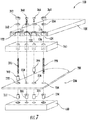
- FIG. 7 depicts an exploded view of an exemplary connector assembly 300 for electrically and mechanically coupling the printed circuit board 120 to the electrical connection structure 230.
- the connector assembly 300 includes a first support bar 130 aligned with the connection structure 230.
- the first support bar 130 can have a degree of rigidity so as to provide mechanical support and protection for the conductor terminals 232, 234, 236, and 238 of the connection structure 230.
- the first support bar 130 can be formed from any insulating or non-conductive material, such as FR4.
- the first support bar 130 can be bonded to the elastomeric patch 110 (shown in FIG. 2 ) through an adhesive, such as Chemlok® adhesive available from LORD Corporation.
- the first support bar 130 can be formed of a hard rubber or other rigid material that is embedded, integral, or a part of the elastomeric patch 110. In this embodiment, no adhesive is necessary to bond the first support bar 130 to the elastomeric patch 110.
- the first support bar 130 can also include rounded or tapered edges so as to reduce the local concentration of stresses applied to the elastomeric patch 110 or to the substrate 200.
- connection assembly 300 can further include a second support bar 140.
- the second support bar 140 can be aligned with the connection structure 230 to protect the conductive terminals 232, 234, 236, and 238 of the connection structure 230.
- the second support bar 140 can also act as a spacer between the substrate 200 and the printed circuit board 120.
- the second support bar 140 can have a height sufficient to prevent the printed circuit board 120 from contacting the substrate 200 when subjected to mechanical stresses, such as during rotation of a tire.
- the second support bar 140 can be formed from an insulating or non-conductive material, such as FR4.
- the plurality of conductive terminals 232, 234, 236, and 238 are arranged between the first support bar 130 and the second support bar 140.
- the first support bar 130 and the second support bar 140 can work together to provide mechanical support and protection for the conductive terminals 232, 234, 236, and 238, including to protect the mechanical integrity of the solder interface at the conductive terminals 232, 234, 236, and 238.
- the first support bar 130 and the second support bar 140 can be compressed together to provide a compressive load on the conductive terminals 232, 234, 236 and 238 of the connection structure 230 to preserve electric contact with the conductive terminals 232, 234, 236, and 238 of the connection structure 230.
- the printed circuit board 120 can be mechanically and electrically connected to the conductive terminals 232, 234, 236, and 238 of the connection structure 230 using conductive posts 310 and 320 and various electrical connectors.
- the first support bar 130 can include a plurality of threaded electrical connectors 332, 334, 336, and 338.
- the electrical connectors 332 and 336 can be non-flanged brass inserts.
- the electrical connectors 334 and 338 can be flanged brass inserts.
- the electrical connectors 334 and 338 can be soldered to the "down" conductive terminals 234 and 238 of the connection structure 230 to provide an electrical connection between the conductive terminals 234, 238 and the electrical connectors 334, 338.
- the connector assembly 300 can also include threaded electrical connectors 342 and 346 that are coupled to the "up" conductive terminals 232 and 236.
- the electrical connectors 342 and 346 can be soldered to the "up" conductive terminals 232 and 236 of the connection structure 230 to provide an electrical connection between the conductive terminals 232, 236 and the electrical connectors 342, 346.
- the electrical connector 342 can be a flanged brass insert. In one implementation, the electrical connector 342 can be aligned with the electrical connector 332 to match threads between the electrical connector 342 and the electrical connector 332.
- the electrical connector 346 can be a threaded stand-off that is threaded into the electrical connector 336.
- the conductive posts 310 and 320 can be arranged in the connector assembly 300 to provide a mechanical and electrical connection between the printed circuit board 120 and the connection structure 230.
- the conductive posts 310 and 320 can be formed from any suitable conductive material such as stainless steel.
- the conductive posts 310 and 320 can include threads for connecting to threaded electrical connectors.
- the conductive post 310 can be electrically coupled to the electrical connector 332 in the first support bar 130 and can be arranged to extend from the first support bar 130 through the conductive terminal 232 and electrical connector 342 and through the second support bar 140.
- the conductive post 310 can then be electrically and mechanically coupled to the printed circuit board 120 using a nut 362 and an optional washer 352 arrangement.
- the nut 362 and optional washer 352 arrangement can be tightened to provide an electrical connection between the conductive post 310 and a conductive terminal 122 on the printed circuit board 120.
- the conductive post 320 can be electrically coupled to the electrical connector 334 in the first support bar 130 and can be arranged to extend from the first support bar 130 through the conductive terminal 234 and through the second support bar 140.
- the conductive post 320 can then be electrically and mechanically coupled to the printed circuit board 120 using a nut 364 and optional washer 354 arrangement.
- the nut 364 and optional washer 354 arrangement can be tightened to provide an electrical connection between the conductive post 320 and a conductive terminal 124 on the printed circuit board 120.
- the conductive post 310 and the conductive post 320 can provide an electrical connection between the printed circuit board 120 and the first piezoelectric component 210 of the substrate 200 via conductive terminals 232 and 234.
- the conductive posts 310 and 320 also act to provide a mechanical connection between the printed circuit board 120 and the substrate 200 and can serve to provide a compressive load on the connection structure 230 by compressing the first support bar 130 and the second support bar 140.
- the printed circuit board 120 can also be electrically coupled to second piezoelectric component 220 of the substrate via electrical connectors 366 and 368.
- electrical connectors 366 and 368 can be coupled, using optional washers 356 and 358 to conductive terminals on the printed circuit board 120.
- the electrical connectors 366 and 368 can be conductive screws.
- the electrical connector 366 can extend through optional washer 356, a conductive terminal 126 of the printed circuit board 120, and the second support bar 140 and be threaded into the stand-off electrical connector 346 so as to provide an electrical connection between a conductive terminal 126 of the printed circuit board 120 and the conductive terminal 236.
- the electrical connector 368 can extend through optional washer 358, a conductive terminal 128 of the printed circuit board 120, the second support bar 140, the conductive terminal 138 and into the electrical connector 338 to provide an electrical connection between a conductive terminal 128 of the printed circuit board 120 and the conductive terminal 238.
- Other suitable electrical connectors can be used in the connector assembly to electrically couple the printed circuit board 120 to the connection structure 230 without deviating from the scope of the present disclosure.
- FIG. 8 depicts a flow diagram of an exemplary method (500) of manufacturing a tire mountable apparatus according to an exemplary embodiment of the present disclosure.
- FIG. 8 depicts steps performed in a particular order for purposes of illustration and discussion, the methods discussed herein are not limited to any particular order or arrangement.
- One skilled in the art, using the disclosures provided herein, will appreciate that various steps of the methods can be omitted, rearranged, combined and/or adapted in various ways.
- the method includes securing electrical connectors to the first support bar. For instance, the electrical connectors 332, 334, 336, and 338 of FIG. 7 can be pressed into the support bar 130.
- the method includes providing solder to the solder wells associated with the "down" conductive terminals of the substrate. For instance, solder can be provided to the solder wells 254 and 258 (shown in FIG. 5 ) associated with down conductive terminals 234 and 238 that are defined in the second insulating layer 250 of the substrate 200.
- the first support bar is aligned with the connection structure of the substrate.
- the first support bar 130 of FIG. 7 with electrical connectors 332, 334, 336, and 338 is aligned with the connection structure 230 of the substrate 200 such that the electrical connectors 332, 334, 336, and 338 are aligned with the conductive terminals 232, 234, 236, and 238 of the connection structure 230.
- electrical connectors are soldered to the down conductive terminals.
- the flanged electrical connectors 334 and 338 are soldered to the down conductive terminals 234 and 238 of the connection structure 230 of the substrate 200.
- the method includes curing the substrate to an elastomeric patch.
- the substrate 200 including the first support bar 130, can be cured with the elastomeric patch 110 to secure the substrate 200 and first support bar 130 to the mesa portion 114 of the elastomeric patch 110.
- the first support bar 130 can be embedded in the elastomeric member 110.
- the substrate 200 can be secured to the elastomeric patch 110 by coating an adhesive on the substrate 200, placing the substrate 200 in a specially designed mold design to accommodate the substrate 200, filling the remainder of the mold with the elastomeric material such as rubber, and curing the patch 110.
- the method includes providing solder to the solder wells associated with the "up" conductive terminals of the substrate.
- solder can be provided to the solder wells 242 and 246 (shown in FIG. 5 ) associated with the up conductive terminals 232 and 236 that are defined in the first insulating layer 240 of the substrate 200.
- electrical connectors are soldered to the up conductive terminals of the substrate.
- the electrical connectors 342 and 346 of FIG. 7 can be soldered to the up conductive terminals 232 and 236.
- the method includes securing conductive posts to the connection structure.
- the conductive post 310 of FIG. 7 can be secured to the electrical connectors 332 and 342 and the conductive terminal 232.
- the conductive post 320 can be secured to the electrical connector 334 and the conductive terminal 234.
- the second support bar is aligned with the connection structure.
- the second support bar 140 of FIG. 7 is positioned over the connection structure 130 such that conductive posts 310 and 320 and electrical connector 346 extend at least partially through the second support bar 140.
- the printed circuit board is secured to the conductive posts.
- the printed circuit board 120 of FIG. 7 is secured to the conductive post 310 using nut 362 and optional washer 352 such that the conductive post 310 is in electrical communication with the conductive terminal 122 of the printed circuit board 120.
- the circuit board 120 is also secured to the conductive post 320 using nut 364 and optional washer 354 such that the conductive post 320 is in electrical communication with the conductive terminal 124 of the printed circuit board 120.
- any remaining electrical connections between the substrate and the printed circuit board are completed.
- the electrical connector 366 of FIG. 7 is threaded through optional washer 356 and conductive terminal 126 of the printed circuit board 120 and into stand-off electrical connector 346.
- the electrical connector 368 is threaded through optional washer 358, conductive terminal 128 of printed circuit board, conductive terminal 238 of the connection structure 230, and the electrical connector 338.
Landscapes
- Engineering & Computer Science (AREA)
- Mechanical Engineering (AREA)
- Microelectronics & Electronic Packaging (AREA)
- Manufacturing & Machinery (AREA)
- Combinations Of Printed Boards (AREA)
- Measuring Fluid Pressure (AREA)
- Coupling Device And Connection With Printed Circuit (AREA)
Description
- The present disclosure relates generally to a piezoelectric device for use as part of a tire patch, and more particularly to an electrical connection structure for a piezoelectric device used as part of a tire patch. The document
US 2011/132649 A1 is an example of prior art, accordingly to the preamble of claim 1. - The incorporation of electronic devices with tire structures has been shown to yield many practical advantages. Piezoelectric devices have been incorporated with tire patches to provide a power source to various sensors and other components of a tire patch used to measure tire parameters. Piezoelectric devices have also been used to acquire data about various physical parameters of a tire during rotation of the tire. Such information may be useful in tire monitoring and warning systems as well as in tire testing and design.
- One known structure for a piezoelectric device includes a substrate having one or more piezoelectric components, such as a power generation component and a signal generation component. Each piezoelectric component can include a sandwich structure that includes a top conductive layer and a lower conductive layer that sandwich a piezoelectric layer. The substrate can include various insulating layers, such as a top insulating layer and a bottom insulating layer to protect and insulate the piezoelectric components. The various piezoelectric components of the piezoelectric device can be electrically coupled to an external device, such as a printed circuit board, using conductive terminals.
- In typical connections for the piezoelectric device, the conductive terminals for the piezoelectric components of the substrate are all located proximate to and are exposed to a single surface of the substrate, such as a top surface of the piezoelectric substrate. In these connections, an electrical connection is made between the conductive terminal located proximate to the top surface of the piezoelectric substrate and a lower conductive layer using a compression connection. This compression connection involves bringing a conductor proximate the top conductive layer in communication with the conductive terminal and a conductor in communication with the lower conductive layer using locally applied high pressure compression techniques to create electrical contact between the conductive terminal and the lower conductive layer.
- For example,
FIG. 1 depicts an exemplarypiezoelectric device 10 having aknown connection structure 30. As shown, theconnection structure 30 includes a plurality ofconductive terminals conductive terminals piezoelectric device 10 through the sameinsulating layer 40 ofpiezoelectric device 10. Certain of theconductive terminals 34 and 36 are coupled to piezoelectric components in thepiezoelectric device 10 throughcompression connections 50. Thecompression connections 50 require a conductor disposed in one layer of thepiezoelectric device 10 to be brought into contact with a conductor disposed in another layer of thepiezoelectric device 10 through high pressure compression. As depicted, the space required forcompression connections 50 can take up valuable real estate on thepiezoelectric device 10. - Given the strain that a piezoelectric device can be subjected to during rotation of a tire, a compression connection coupling a conductive terminal to a lower conductive layer in a piezoelectric device can be disrupted or can fail during use of the piezoelectric device. In addition, in many applications, a relatively rigid material, such as FR4, is used for the insulating layers of the substrate. It can be difficult to create workable compression connections through these rigid insulating layers using locally applied high pressure compression techniques.
- Thus, a need exists for an improved electrical connection structure for a piezoelectric device. A connection structure that readily allows for incorporation of the piezoelectric device into a tire patch would be particularly useful.
- Aspects and advantages of the invention will be set forth in part in the following description, or may be apparent from the description, or may be learned through practice of the invention.
- One exemplary aspect of the present disclosure is directed to a tire mountable apparatus. The tire mountable apparatus includes a substrate that has a piezoelectric component. The piezoelectric component includes first and second conductive layers and a piezoelectric layer arranged between the first and second conductive layers. The substrate further includes a first insulating layer disposed on the first conductive layer and a second insulating layer disposed on the second conductive layer such that the piezoelectric component is arranged between the first insulating layer and the second insulating layer in the substrate. The substrate further includes a conductive terminal structure. The conductive terminal structure includes a plurality of conductive terminals, including a first conductive terminal electrically coupled to the first conductive layer and a second conductive terminal electrically coupled to the second conductive layer. The first conductive terminal is exposed through the first insulating layer of the substrate and the second conductive terminal is exposed through the second insulating layer of the substrate.
- Another exemplary aspect of the present disclosure is directed to a method of manufacturing a tire mountable apparatus. The method includes aligning a first support bar with a plurality of conductive terminals formed in a substrate, the substrate comprising a piezoelectric component arranged between a first insulating layer and a second insulating layer. The plurality of conductive terminals include a first conductive terminal exposed through the first insulating layer of the substrate and a second conductive terminal exposed through the second insulating layer of the substrate. The method further includes providing solder in a second solder well formed in the second insulating layer of the substrate. The second solder well is associated with the second conductive terminal. The method further includes soldering an electrical connector located in the first support bar with the second conductive terminal.
- In a particular implementation of this exemplary aspect of the present disclosure, the method can further include providing solder in a first solder well formed in the first insulating layer of the substrate. The first solder well can be associated with the first conductive terminal. The method can further include soldering an electrical connector with the first conductive terminal.
- These and other features, aspects and advantages of the present invention will become better understood with reference to the following description and appended claims. The accompanying drawings, which are incorporated in and constitute a part of this specification, illustrate embodiments of the invention and, together with the description, serve to explain the principles of the invention.
- A full and enabling disclosure of the present invention, including the best mode thereof, directed to one of ordinary skill in the art, is set forth in the specification, which makes reference to the appended figures, in which:
-
FIG. 1 depicts a plan view of a piezoelectric device having a known connection structure; -
FIG. 2 depicts an exploded view of an exemplary tire mountable apparatus according to an exemplary embodiment of the present disclosure; -
FIG. 3 depicts a cross-sectional view of a substrate including a piezoelectric component according to an exemplary embodiment of the present disclosure; -
FIG. 4 depicts a plan view of a first surface of a substrate including a conductive terminal structure according to an exemplary embodiment of the present disclosure; -
FIG. 5 depicts a plan view of a second surface of a substrate including a conductive terminal structure according to an exemplary embodiment of the present disclosure; -
FIG. 6 depicts a cross-sectional view of a conductive terminal structure according to an exemplary embodiment of the present disclosure; -
FIG. 7 depicts an exploded view of a tire mountable apparatus according to an exemplary embodiment of the present disclosure; and -
FIG. 8 depicts a flow diagram of an exemplary method according to an exemplary embodiment of the present disclosure. - Reference now will be made in detail to embodiments of the invention, one or more examples of which are illustrated in the drawings. Each example is provided by way of explanation of the invention, not limitation of the invention. In fact, it will be apparent to those skilled in the art that various modifications and variations can be made in the present invention without departing from the scope or spirit of the invention. For instance, features illustrated or described as part of one embodiment can be used with another embodiment to yield a still further embodiment. Thus, it is intended that the present invention covers such modifications and variations as come within the scope of the appended claims and their equivalents.
- Generally, the present disclosure is directed to an improved conductive terminal structure for a piezoelectric device used as part of a tire mountable apparatus, such as a tire patch that can be incorporated with a tire to measure various parameters of the tire. In particular, a piezoelectric device can include one or more piezoelectric components that are used to harvest energy and/or to provide signals indicative of tire rotation/strain. The piezoelectric components can have a sandwich structure that includes a piezoelectric layer, such as a lead zirconate titanate (PZT) layer, arranged between a pair of conductive layers. The piezoelectric components can be arranged between a pair of insulating layers, such as FR4 layers. The piezoelectric device can be implemented as a substrate or can take any other suitable form, such as a film. An electrical connection structure can be provided in the piezoelectric device to electrically connect the piezoelectric components to a printed circuit board or other device used as part of the tire patch. The piezoelectric components can provide energy and/or signals through the electrical connection structure to various devices located on the printed circuit board.
- Unlike known electrical connection structures which include a plurality of conductive terminals that are all exposed through a single insulating layer of the substrate, such as a top layer of the substrate, the electrical connection structure according to aspects of the present disclosure are arranged in a one up, one down configuration. In this configuration, at least one conductive terminal that is electrically coupled to a top conductive layer of a piezoelectric component is exposed through a top insulating layer of the substrate. In addition, at least one conductive terminal that is electrically coupled to a bottom conductive layer of a piezoelectric component is exposed through a bottom insulating layer of the substrate. As a result, at least one pair of conductive terminals of the electrical connection structure are exposed for electrical connection through opposite surfaces of the substrate such that there is at least one "up" conductive terminal and one "down" conductive terminal.
- The one up, one down electrical connection structure according to aspects of the present disclosure eliminates the need for compression connections to electrically couple conductive terminals with conductive layers of a piezoelectric component. Elimination of compression connections provides many advantages. For instance, elimination of compression connections improves the durability of the electrical connections between the piezoelectric components and the printed circuit board, leading to increased reliability and performance life of the tire patch. Moreover, a relatively rigid material, such as FR4 material, can be used as the insulating layers of the substrate without affecting the quality of electrical connections within the substrate.
- According to particular aspects of the present disclosure, the one up, one down electrical connection structure can be used in combination with a connector assembly design to preserve the integrity of the electrical connection between the electrical connection structure and the printed circuit board. For instance, the electrical connection structure can be arranged between a first support bar and a second support bar. An electrical connector disposed in the first support bar can be soldered to a "down" conductive terminal exposed through the layer of insulating material adjacent to the first support bar. Similarly, an electrical connector can be soldered to an "up" conductive terminal exposed through the layer of insulating material adjacent the second support bar. The printed circuit board can be electrically and mechanically coupled to the electrical connection structure using conductive posts, such as threaded rods, that can be used to compress the connection structure between the first and second support bars. As a result, the electrical interface between the printed circuit board and the electrical connection structure can be chemically and electrically preserved using ordinary solder and a compressive load.
- Referring now to the FIGS., exemplary embodiments of the present disclosure will now be discussed in detail.
FIG. 2 depicts an exploded view of an exemplary tire mountable apparatus 100 (e.g. a tire patch) according to an exemplary embodiment of the present disclosure. The tiremountable apparatus 100 can be secured to a tire, such as the inner liner of a pneumatic tire, to monitor various parameters of the tire. - As illustrated, the tire
mountable apparatus 100 includes asubstrate 200 having a length L and a width W. As illustrated, the width W of thesubstrate 200 is significantly less than the length L. For instance, the length L can be at least twice the width W. In this regard, the tire mountable apparatus can be considered a 1-D tiremountable apparatus 100 because the length L dimension is significantly larger than the width W dimension. As can be seen fromFIG. 2 , however, the 1-D tiremountable apparatus 100 actually has three dimensions. - The
substrate 200 can be secured to anelastomeric patch 110 that includes abase portion 112 and a raisedmesa portion 114 having a height H above thebase portion 112 of theelastomeric patch 110. Theelastomeric patch 110 can be formed from an elastomeric material, such as a rubber material normally employed as a sidewall material in the construction of pneumatic tires. In one example, thesubstrate 200 can be secured to theelastomeric patch 110 by coating an adhesive on thesubstrate 200, placing thesubstrate 200 in a specially designed mold designed to accommodate thesubstrate 200, filling the remainder of the mold with the elastomeric material, and curing thepatch 110. - As illustrated in
FIG. 2 , thesubstrate 200 includes a firstpiezoelectric component 210 and a secondpiezoelectric component 220. The firstpiezoelectric component 210 can be a generator piezoelectric component that is used to harvest energy upon flexure of the firstpiezoelectric component 210. The secondpiezoelectric component 220 can be a signal/sensor piezoelectric component that is used to provide electrical signals for analysis upon flexure of the secondpiezoelectric component 220. The electrical signals provided by the secondpiezoelectric component 220 can be analyzed, for instance, to determine characteristics of the contact patch of a tire or to count revolutions of a tire. - Each of the
piezoelectric components FIG. 3 depicts a cross-sectional view of thepiezoelectric component 210 ofsubstrate 200. Thepiezoelectric component 210 includes apiezoelectric layer 216 arranged between a firstconductive layer 212 on a first side of thepiezoelectric layer 216 and a secondconductive layer 214 on a second side of thepiezoelectric layer 216. Thepiezoelectric layer 216 can be formed from any suitable piezoelectric material, such as a PZT material. Theconductive layers - As illustrated in
FIG. 3 , thepiezoelectric component 210 is arranged between a first insulatinglayer 240 of thesubstrate 200 and a second insulatinglayer 250 of thesubstrate 200. Due to the strain thesubstrate 200 is subjected to during rotation of the tire, the first insulatinglayer 240 and the second insulatinglayer 250 can be formed from a relatively rigid material, such as the fire resistant material FR4 or other suitable materials. In one aspect, the second insulatinglayer 250 can be thicker than the insulatinglayer 240 to offset thepiezoelectric layer 216 from a neutral plane off thesubstrate 200 to increase energy generation upon flexure of thepiezoelectric component 210. - Referring back to
FIG. 2 , the tiremountable apparatus 100 can further include a printedcircuit board 120. The printedcircuit board 120 can include various components and devices, such as a microprocessor, a memory, temperature and/or pressure sensors, filter circuits, communication circuits, a battery, one or more antennas for communicating information to remote devices, and other devices. Thegenerator piezoelectric component 210 can provide energy upon flexure of thepiezoelectric component 210 to power the various components of the printedcircuit board 120. Thesignal piezoelectric component 220 can provide signals associated with strain induced in a tire upon flexure of thepiezoelectric component 220 to the printed circuit board for analysis. - As will be discussed in more detail below, the printed
circuit board 120 can be electrically coupled to thegenerator piezoelectric component 210 and thesignal piezoelectric component 220 of the substrate through a one up, one downelectrical connection structure 230. Theconnection structure 230 can include a plurality of conductive terminals. While four conductive terminals are depicted inFIG. 2 , those of ordinary skill in the art, using the disclosures provided herein, will understand that more or fewer conductive terminals can be provided without deviating from the scope of the present disclosure. - As shown in
FIG. 2 , the plurality of conductive terminals can be arranged in a generally linear relationship. It should be appreciated that as used herein, the phrase "generally linear relationship" is intended to signify that there may be a variation in alignment from a perfect linear relationship. The conductive terminals can be arranged along a line perpendicular to the length of thesubstrate 200 such that mechanical strain applied to the conductive terminals during use can be reduced. - The one up, one down
connection structure 230 arranges the plurality of conductive terminals such that at least one conductive terminal is exposed through a top surface of thesubstrate 200 and at least one other conductive terminal is exposed through a bottom surface of thesubstrate 200. Theconnection structure 230 can be arranged between afirst support bar 130 and asecond support bar 140 which can be used to provide a compressive load to theconnection structure 230. This compressive load can be used to ensure the chemical and electrical integrity of the electrical connection between the printedcircuit board 140 and theelectrical connection structure 230 using ordinary solder connections as will be discussed in more detail below. - Exemplary aspects of the one up, one down
connection structure 230 will be discussed with reference toFIGS. 4-6 .FIG. 4 depicts a top plan view of thesubstrate 200 including a one up, one downconnection structure 230 according to an exemplary embodiment of the present disclosure. Theconnection structure 230 includes a firstconductive terminal 232 electrically coupled to the firstconductive layer 212 of thepiezoelectric component 210 via a suitableconductive trace 233. The firstconductive terminal 232 includes a conductive annulus or other suitable conductive structure that is exposed to the top surface of thesubstrate 200 through the first insulatinglayer 240 of thesubstrate 200. -
FIG. 5 depicts a plan view of the opposite surface of thesubstrate 200. As shown, theconnection structure 230 includes a secondconductive terminal 234 electrically coupled to the secondconductive layer 214 of thepiezoelectric component 210 via a suitableconductive trace 235. The secondconductive terminal 234 includes a conductive annulus or other suitable conductive structure that is exposed to the bottom surface of thesubstrate 200 through the second insulatinglayer 250 of thesubstrate 200. In this way, thepiezoelectric component 210 includes oneconductive terminal 232 exposed through the first insulatinglayer 240 and anotherconductive terminal 234 exposed through the second insulatinglayer 250. No compression connections are required to couple the firstconductive terminal 232 to the firstconductive layer 212 of thepiezoelectric component 210 or to couple the secondconductive terminal 234 to the secondconductive layer 214 of thepiezoelectric component 210. - Referring back to
FIG. 4 , theconnection structure 230 can further include a thirdconductive terminal 236 electrically coupled to the firstconductive layer 222 of the secondpiezoelectric component 220 via a suitableconductive trace 237. The thirdconductive terminal 236 includes a conductive annulus or other suitable conductive structure that is exposed to the top surface of thesubstrate 200 through the first insulatinglayer 240. - As shown in
FIG. 5 , theconnection structure 230 can also include a fourthconductive terminal 238 electrically coupled to the secondconductive layer 224 of thepiezoelectric component 220 via a suitableconductive trace 239. The fourthconductive terminal 238 includes a conductive annulus or other suitable conductive structure that is exposed to the bottom surface of thesubstrate 200 through the second insulatinglayer 250 of thesubstrate 200. In this way, thepiezoelectric component 220 includes oneconductive terminal 236 exposed through the first insulatinglayer 240 and anotherconductive terminal 238 exposed through the second insulatinglayer 250. Similar to theconductive terminals piezoelectric component 210, no compression connections are required to couple the thirdconductive terminal 236 to the firstconductive layer 222 of thepiezoelectric component 220 or to couple the secondconductive terminal 238 to the secondconductive layer 224 of thepiezoelectric component 220. -
FIG. 6 depicts a cross-sectional view taken along line 6-6' of theconnection structure 230 of thesubstrate 200 ofFIG. 4 .FIG. 6 illustrates that theconductive terminals piezoelectric component 210 are exposed on opposite sides of thesubstrate 200. In particular,conductive terminal 232 is exposed through the first insulatinglayer 240. Theconductive terminal 234 is exposed through the second insulatinglayer 250. Theconductive terminal 232 can be electrically coupled to a firstconductive layer 212 of the piezoelectric component 210 (shown inFIG. 4 ). Theconductive terminal 234 can be electrically coupled to a secondconductive layer 214 of the piezoelectric component 210 (shown inFIG. 5 ). Referring toFIG. 6 , theconductive terminal 232 includes a solder well 242 formed in the first insulatinglayer 240. Theconductive terminal 234 includes a solder well 254 formed in the second insulatinglayer 250. Thesolder wells -
FIG. 6 further illustrates that theconductive terminal piezoelectric component 220 are exposed on opposite sides of thesubstrate 200. In particular,conductive terminal 236 is exposed through the first insulatinglayer 240. Theconductive terminal 238 is exposed through the second insulatinglayer 250. Theconductive terminal 236 can be electrically coupled to a firstconductive layer 222 of the piezoelectric component 220 (shown inFIG. 4 ). Theconductive terminal 238 can be electrically coupled to a secondconductive layer 224 of the piezoelectric component 220 (shown inFIG. 5 ). Similar to theconductive terminals conductive terminal 236 includes a solder well 246 formed in the first insulatinglayer 240. Theconductive terminal 238 includes a solder well 258 formed in the second insulatinglayer 250. Thesolder wells -
FIGS. 4-6 depict one exemplary configuration of a one up, one down configuration for an electrical connection structure providing connections topiezoelectric components signal piezoelectric component 210. The inner conductive terminals can be coupled to thegenerator piezoelectric component 220. Other suitable configurations are also possible. -
FIG. 7 depicts an exploded view of anexemplary connector assembly 300 for electrically and mechanically coupling the printedcircuit board 120 to theelectrical connection structure 230. As shown, theconnector assembly 300 includes afirst support bar 130 aligned with theconnection structure 230. Thefirst support bar 130 can have a degree of rigidity so as to provide mechanical support and protection for theconductor terminals connection structure 230. Thefirst support bar 130 can be formed from any insulating or non-conductive material, such as FR4. - The
first support bar 130 can be bonded to the elastomeric patch 110 (shown inFIG. 2 ) through an adhesive, such as Chemlok® adhesive available from LORD Corporation. In another embodiment, thefirst support bar 130 can be formed of a hard rubber or other rigid material that is embedded, integral, or a part of theelastomeric patch 110. In this embodiment, no adhesive is necessary to bond thefirst support bar 130 to theelastomeric patch 110. Thefirst support bar 130 can also include rounded or tapered edges so as to reduce the local concentration of stresses applied to theelastomeric patch 110 or to thesubstrate 200. - Referring back to
FIG. 7 , theconnection assembly 300 can further include asecond support bar 140. Thesecond support bar 140 can be aligned with theconnection structure 230 to protect theconductive terminals connection structure 230. Thesecond support bar 140 can also act as a spacer between thesubstrate 200 and the printedcircuit board 120. Thesecond support bar 140 can have a height sufficient to prevent the printedcircuit board 120 from contacting thesubstrate 200 when subjected to mechanical stresses, such as during rotation of a tire. Similar to thefirst support bar 130, thesecond support bar 140 can be formed from an insulating or non-conductive material, such as FR4. - As shown in
FIG. 7 , the plurality ofconductive terminals first support bar 130 and thesecond support bar 140. Thefirst support bar 130 and thesecond support bar 140 can work together to provide mechanical support and protection for theconductive terminals conductive terminals first support bar 130 and thesecond support bar 140 can be compressed together to provide a compressive load on theconductive terminals connection structure 230 to preserve electric contact with theconductive terminals connection structure 230. - The printed
circuit board 120 can be mechanically and electrically connected to theconductive terminals connection structure 230 usingconductive posts first support bar 130 can include a plurality of threadedelectrical connectors electrical connectors electrical connectors electrical connectors conductive terminals connection structure 230 to provide an electrical connection between theconductive terminals electrical connectors - The
connector assembly 300 can also include threadedelectrical connectors conductive terminals electrical connectors conductive terminals connection structure 230 to provide an electrical connection between theconductive terminals electrical connectors electrical connector 342 can be a flanged brass insert. In one implementation, theelectrical connector 342 can be aligned with theelectrical connector 332 to match threads between theelectrical connector 342 and theelectrical connector 332. Theelectrical connector 346 can be a threaded stand-off that is threaded into theelectrical connector 336. - The
conductive posts connector assembly 300 to provide a mechanical and electrical connection between the printedcircuit board 120 and theconnection structure 230. Theconductive posts conductive posts - The
conductive post 310 can be electrically coupled to theelectrical connector 332 in thefirst support bar 130 and can be arranged to extend from thefirst support bar 130 through theconductive terminal 232 andelectrical connector 342 and through thesecond support bar 140. Theconductive post 310 can then be electrically and mechanically coupled to the printedcircuit board 120 using anut 362 and anoptional washer 352 arrangement. In particular, thenut 362 andoptional washer 352 arrangement can be tightened to provide an electrical connection between theconductive post 310 and aconductive terminal 122 on the printedcircuit board 120. - The
conductive post 320 can be electrically coupled to theelectrical connector 334 in thefirst support bar 130 and can be arranged to extend from thefirst support bar 130 through theconductive terminal 234 and through thesecond support bar 140. Theconductive post 320 can then be electrically and mechanically coupled to the printedcircuit board 120 using anut 364 andoptional washer 354 arrangement. In particular, thenut 364 andoptional washer 354 arrangement can be tightened to provide an electrical connection between theconductive post 320 and aconductive terminal 124 on the printedcircuit board 120. - The
conductive post 310 and theconductive post 320, together, can provide an electrical connection between the printedcircuit board 120 and the firstpiezoelectric component 210 of thesubstrate 200 viaconductive terminals conductive posts circuit board 120 and thesubstrate 200 and can serve to provide a compressive load on theconnection structure 230 by compressing thefirst support bar 130 and thesecond support bar 140. - The printed
circuit board 120 can also be electrically coupled to secondpiezoelectric component 220 of the substrate viaelectrical connectors electrical connectors optional washers circuit board 120. Theelectrical connectors electrical connector 366 can extend throughoptional washer 356, aconductive terminal 126 of the printedcircuit board 120, and thesecond support bar 140 and be threaded into the stand-offelectrical connector 346 so as to provide an electrical connection between aconductive terminal 126 of the printedcircuit board 120 and theconductive terminal 236. - The
electrical connector 368 can extend throughoptional washer 358, aconductive terminal 128 of the printedcircuit board 120, thesecond support bar 140, the conductive terminal 138 and into theelectrical connector 338 to provide an electrical connection between aconductive terminal 128 of the printedcircuit board 120 and theconductive terminal 238. Other suitable electrical connectors can be used in the connector assembly to electrically couple the printedcircuit board 120 to theconnection structure 230 without deviating from the scope of the present disclosure. -
FIG. 8 depicts a flow diagram of an exemplary method (500) of manufacturing a tire mountable apparatus according to an exemplary embodiment of the present disclosure. AlthoughFIG. 8 depicts steps performed in a particular order for purposes of illustration and discussion, the methods discussed herein are not limited to any particular order or arrangement. One skilled in the art, using the disclosures provided herein, will appreciate that various steps of the methods can be omitted, rearranged, combined and/or adapted in various ways. - At (502), the method includes securing electrical connectors to the first support bar. For instance, the
electrical connectors FIG. 7 can be pressed into thesupport bar 130. At (504), the method includes providing solder to the solder wells associated with the "down" conductive terminals of the substrate. For instance, solder can be provided to thesolder wells 254 and 258 (shown inFIG. 5 ) associated with downconductive terminals layer 250 of thesubstrate 200. - At (506) of
FIG. 8 , the first support bar is aligned with the connection structure of the substrate. For instance, thefirst support bar 130 ofFIG. 7 withelectrical connectors connection structure 230 of thesubstrate 200 such that theelectrical connectors conductive terminals connection structure 230. At (508) of FIG. 9, electrical connectors are soldered to the down conductive terminals. For instance, the flangedelectrical connectors conductive terminals connection structure 230 of thesubstrate 200. - At (510) of
FIG. 8 , the method includes curing the substrate to an elastomeric patch. For instance, as shown inFIG. 1 , thesubstrate 200, including thefirst support bar 130, can be cured with theelastomeric patch 110 to secure thesubstrate 200 andfirst support bar 130 to themesa portion 114 of theelastomeric patch 110. Thefirst support bar 130 can be embedded in theelastomeric member 110. In one example, thesubstrate 200 can be secured to theelastomeric patch 110 by coating an adhesive on thesubstrate 200, placing thesubstrate 200 in a specially designed mold design to accommodate thesubstrate 200, filling the remainder of the mold with the elastomeric material such as rubber, and curing thepatch 110. - At (512) of
FIG. 8 , the method includes providing solder to the solder wells associated with the "up" conductive terminals of the substrate. For instance, solder can be provided to thesolder wells 242 and 246 (shown inFIG. 5 ) associated with the upconductive terminals layer 240 of thesubstrate 200. At (514) ofFIG. 8 , electrical connectors are soldered to the up conductive terminals of the substrate. For instance, theelectrical connectors FIG. 7 can be soldered to the upconductive terminals - At (516) of
FIG. 8 , the method includes securing conductive posts to the connection structure. For instance, theconductive post 310 ofFIG. 7 can be secured to theelectrical connectors conductive terminal 232. Theconductive post 320 can be secured to theelectrical connector 334 and theconductive terminal 234. - At (518) of
FIG. 8 , the second support bar is aligned with the connection structure. For instance, thesecond support bar 140 ofFIG. 7 is positioned over theconnection structure 130 such thatconductive posts electrical connector 346 extend at least partially through thesecond support bar 140. At (520) ofFIG. 8 , the printed circuit board is secured to the conductive posts. For instance, the printedcircuit board 120 ofFIG. 7 is secured to theconductive post 310 usingnut 362 andoptional washer 352 such that theconductive post 310 is in electrical communication with theconductive terminal 122 of the printedcircuit board 120. Thecircuit board 120 is also secured to theconductive post 320 usingnut 364 andoptional washer 354 such that theconductive post 320 is in electrical communication with theconductive terminal 124 of the printedcircuit board 120. - At (522) of
FIG. 8 , any remaining electrical connections between the substrate and the printed circuit board are completed. For instance, theelectrical connector 366 ofFIG. 7 is threaded throughoptional washer 356 andconductive terminal 126 of the printedcircuit board 120 and into stand-offelectrical connector 346. Theelectrical connector 368 is threaded throughoptional washer 358,conductive terminal 128 of printed circuit board,conductive terminal 238 of theconnection structure 230, and theelectrical connector 338.
Claims (12)
- A tire mountable apparatus (100) comprising a substrate (200), the substrate (200) comprising:a first piezoelectric component (210), the first piezoelectric component (210) comprising first and second conductive layers (212, 214) and a piezoelectric layer (216) arranged between the first and second conductive layers (212, 214);a second piezoelectric component (220) arranged between the first insulating layer (240) and the second insulating layer (250), the second piezoelectric component (220) comprising third and fourth conductive layers (222, 224) and a second piezoelectric layer arranged between the third and fourth conductive layers (222, 224);a first insulating layer (240) disposed on the first and third conductive layer (212, 222) and a second insulating layer (250) disposed on the second and fourth conductive layer (214, 224) such that the first and second piezoelectric component (210, 220) are arranged between the first insulating layer (240) and the second insulating layer (250) in the substrate (200); anda conductive terminal structure,characterized in thatthe conductive terminal structure comprises a plurality of conductive terminals, the plurality of conductive terminals comprising a first conductive terminal (232) electrically coupled to the first conductive layer (212), a second conductive terminal (234) electrically coupled to the second conductive layer (214), a third conductive terminal (236) electrically coupled to the third conductive layer (222) and a fourth conductive terminal (238) electrically coupled to the fourth conductive layer (224);wherein the first conductive terminal (232) is exposed through the first insulating layer (240) of the substrate (200) and the second conductive terminal (234) is exposed through the second insulating layer (250) of the substrate (200), wherein the third conductive terminal (236) is exposed through the first insulating layer (240) of the substrate (200) and the fourth conductive terminal (238) is exposed through the second insulating layer (250) of the substrate (200).
- The tire mountable apparatus (100) of claim 1, wherein the first conductive terminal (232) comprises a first solder well (242) formed in the first insulating layer (240) and the second conductive terminal (234) comprises a second solder well (254) formed in the second insulating layer (250).
- The tire mountable apparatus (100) of claim 1, wherein the plurality of conductive terminals are arranged in a generally linear relationship.
- The tire mountable apparatus (100) of claim 1, wherein the third conductive terminal (236) comprises a third solder well (246) formed in the first insulating layer and the fourth conductive terminal (238) comprises a fourth solder well (258) formed in the second insulating layer (250).
- The tire mountable apparatus (100) of claim 1, wherein the plurality of conductive terminals each comprise a conductive annulus.
- The tire mountable apparatus (100) of claim 1, wherein the first and second insulating layers (240, 250) are formed from FR4.
- A method of manufacturing a tire mountable apparatus (100), comprising:aligning a first support bar (130) with a plurality of conductive terminals formed in a substrate (200), the substrate (200) comprising a first piezoelectric component (210) arranged between a first insulating layer (240) and a second insulating layer (250) and a second piezoelectric component (220) arranged between the first insulating layer (240) and the second insulating layer (250), the first piezoelectric component (210) comprising first and second conductive layers (212, 214) and a piezoelectric layer (216) arranged between the first and second conductive layers (212, 214), the second piezoelectric component (220) comprising third and fourth conductive layers (222, 224) and a second piezoelectric layer arranged between the third and fourth conductive layers (222, 224), the plurality of conductive terminals comprising a first conductive terminal (232) coupled to the first conductive layer (212) exposed through the first insulating layer (240) of the substrate (200), a second conductive terminal (234) coupled to the second conductive layer (214) exposed through the second insulating layer (250) of the substrate (200), a third conductive terminal (236) coupled to the third conductive layer (222) exposed through the first insulating layer (240), and a fourth conductive terminal (238) coupled to the fourth conductive layer (224) exposed through the second insulating layer (250);providing solder in a second solder well (254) formed in the second insulating layer (250) of the substrate (200), the second solder well (254) associated with the second conductive terminal (234); andsoldering an electrical connector located in the first support bar (130) with the second conductive terminal (234).
- The method of claim 7, wherein the method further comprises curing the substrate (200) to an elastomeric member (110), the elastomeric member (110) comprising a base portion (112) and a mesa portion (114), the substrate (200) being secured to the mesa portion (114) of the elastomeric member (110) such that the first support bar (130) is embedded in the elastomeric member (110).
- The method of claim 7, wherein the method further comprises:providing solder in a first solder well (242) formed in the first insulating layer (240) of the substrate (200), the first solder well (242) associated with the first conductive terminal (232); andsoldering an electrical connector with the first conductive terminal (232).
- The method of claim 9, wherein the method further comprises:securing a first conductive post (310) to the electrical connector soldered to the first conductive terminal (332); andsecuring a second conductive post (320) to the electrical connector soldered to the second conductive terminal (234).
- The method of claim 10, wherein the method comprises positioning a second support bar (140) over the plurality of conductive terminals such that the first and second conductive posts (310, 320) extend through the second support bar (140).
- The method of claim 11, wherein the method comprises securing a printed circuit board (120) to the first and second conductive posts (310, 320) such that the printed circuit board (120) is electrically connected to the first and second conductive terminals (232, 234) and such that the printed circuit board (120) is mechanically supported by the first and second conductive posts (310,320).
Applications Claiming Priority (1)
| Application Number | Priority Date | Filing Date | Title |
|---|---|---|---|
| PCT/US2012/065259 WO2014077816A2 (en) | 2012-11-15 | 2012-11-15 | One up, one down connection structure for piezoelectric device in tire patch |
Publications (3)
| Publication Number | Publication Date |
|---|---|
| EP2920009A2 EP2920009A2 (en) | 2015-09-23 |
| EP2920009A4 EP2920009A4 (en) | 2016-08-24 |
| EP2920009B1 true EP2920009B1 (en) | 2018-01-03 |
Family
ID=50731800
Family Applications (1)
| Application Number | Title | Priority Date | Filing Date |
|---|---|---|---|
| EP12888379.0A Active EP2920009B1 (en) | 2012-11-15 | 2012-11-15 | One up, one down connection structure for piezoelectric device in tire patch |
Country Status (6)
| Country | Link |
|---|---|
| US (1) | US9780287B2 (en) |
| EP (1) | EP2920009B1 (en) |
| JP (1) | JP6342896B2 (en) |
| KR (1) | KR101696631B1 (en) |
| CN (1) | CN104903125B (en) |
| WO (1) | WO2014077816A2 (en) |
Families Citing this family (5)
| Publication number | Priority date | Publication date | Assignee | Title |
|---|---|---|---|---|
| WO2016053347A1 (en) | 2014-10-03 | 2016-04-07 | Compagnie Generale Des Etablissements Michelin | Durable electrical signal connector to isolate mechanical and electrical function |
| WO2016053348A1 (en) | 2014-10-03 | 2016-04-07 | Compagnie Generale Des Etablissements Michelin | Profiled element for durable electrical signal connector |
| EP4010209B1 (en) * | 2019-08-05 | 2025-02-19 | Bridgestone Americas Tire Operations, LLC | Daisy tire electronics assembly |
| CN114340915B (en) * | 2019-08-05 | 2024-08-06 | 普利司通美国轮胎运营有限责任公司 | Tire electronics assembly |
| JP2024516636A (en) * | 2021-04-30 | 2024-04-16 | テクスキャン インコーポレイテッド | Contact Sensor |
Family Cites Families (11)
| Publication number | Priority date | Publication date | Assignee | Title |
|---|---|---|---|---|
| BR9912848A (en) * | 1998-08-03 | 2001-05-08 | Goodyear Tire & Rubber | Assembly of transponders in tires |
| CN100470867C (en) * | 2003-09-04 | 2009-03-18 | 日本电气株式会社 | Piezoelectric ceramic transducers and portable devices |
| US20050076982A1 (en) * | 2003-10-09 | 2005-04-14 | Metcalf Arthur Richard | Post patch assembly for mounting devices in a tire interior |
| JP2005331070A (en) | 2004-05-21 | 2005-12-02 | Toyota Motor Corp | Method for mounting vibration damping piezoelectric element and piezoelectric vibration damping device |
| CN101052538A (en) * | 2004-11-12 | 2007-10-10 | 米其林技术公司 | Tread fixture patch for fixture rigid structure of tyres |
| CN102077332B (en) * | 2008-06-26 | 2014-05-14 | 米其林研究和技术股份有限公司 | Sandwich piezoelectric device with solid copper electrode |
| JP5928935B2 (en) | 2008-08-29 | 2016-06-01 | カンパニー ジェネラレ デ エスタブリシュメンツ ミシュラン | Equipment for 1-D tires |
| US8742265B2 (en) | 2008-08-29 | 2014-06-03 | Compagnie Generale Des Etablissements Michelin | 1-D tire patch apparatus and methodology |
| CN102396145B (en) | 2009-04-15 | 2014-03-05 | 株式会社村田制作所 | piezoelectric generator |
| JP2011071389A (en) | 2009-09-28 | 2011-04-07 | Fujifilm Corp | In-tire power generator, and tire monitoring system using the same |
| JP5984523B2 (en) * | 2012-06-15 | 2016-09-06 | キヤノン株式会社 | Vibration wave drive |
-
2012
- 2012-11-15 KR KR1020157012507A patent/KR101696631B1/en not_active Expired - Fee Related
- 2012-11-15 CN CN201280075506.8A patent/CN104903125B/en active Active
- 2012-11-15 EP EP12888379.0A patent/EP2920009B1/en active Active
- 2012-11-15 JP JP2015528448A patent/JP6342896B2/en not_active Expired - Fee Related
- 2012-11-15 US US14/417,346 patent/US9780287B2/en active Active
- 2012-11-15 WO PCT/US2012/065259 patent/WO2014077816A2/en not_active Ceased
Non-Patent Citations (1)
| Title |
|---|
| None * |
Also Published As
| Publication number | Publication date |
|---|---|
| JP6342896B2 (en) | 2018-06-13 |
| CN104903125B (en) | 2018-02-02 |
| EP2920009A2 (en) | 2015-09-23 |
| KR101696631B1 (en) | 2017-01-16 |
| EP2920009A4 (en) | 2016-08-24 |
| WO2014077816A3 (en) | 2015-08-06 |
| CN104903125A (en) | 2015-09-09 |
| KR20150070289A (en) | 2015-06-24 |
| WO2014077816A2 (en) | 2014-05-22 |
| US9780287B2 (en) | 2017-10-03 |
| US20150249198A1 (en) | 2015-09-03 |
| JP2015533700A (en) | 2015-11-26 |
Similar Documents
| Publication | Publication Date | Title |
|---|---|---|
| US7656076B1 (en) | Unimorph/bimorph piezoelectric package | |
| US20140215785A1 (en) | 1-D Tire Patch Apparatus and Methodology | |
| US8742265B2 (en) | 1-D tire patch apparatus and methodology | |
| US7737708B2 (en) | Contact for use in testing integrated circuits | |
| US9780287B2 (en) | One up, one down connection structure for piezoelectric device in tire patch | |
| JP4555362B2 (en) | Probe, electronic component testing apparatus, and probe manufacturing method | |
| US4417170A (en) | Flexible circuit interconnect for piezoelectric element | |
| JP5743040B2 (en) | Flexible circuit board and method for manufacturing flexible circuit board | |
| US20080218026A1 (en) | Piezoelectric package with enlarged conductive layers | |
| US8546998B2 (en) | Sandwich piezoelectric device with solid copper electrode | |
| KR20160041761A (en) | Probe card | |
| CN102735883A (en) | Electrical interconnect device | |
| US8385081B2 (en) | Stacked mounting structure | |
| KR102827418B1 (en) | Electromechanical converter with layered structure | |
| JP2010043868A (en) | Electric inspection jig and electric inspection apparatus | |
| US7629728B1 (en) | Scalable piezoelectric package | |
| WO2010008381A1 (en) | Unimorph/bimorph piezoelectric package | |
| JP4848676B2 (en) | Component-embedded substrate, component-embedded module using the component-embedded substrate, and method of manufacturing the component-embedded substrate | |
| KR20180005904A (en) | Combination structure of battery sensor module for vehicle | |
| HK1111226A (en) | Contact for use in testing integrated circuits |
Legal Events
| Date | Code | Title | Description |
|---|---|---|---|
| PUAI | Public reference made under article 153(3) epc to a published international application that has entered the european phase |
Free format text: ORIGINAL CODE: 0009012 |
|
| 17P | Request for examination filed |
Effective date: 20150410 |
|
| AK | Designated contracting states |
Kind code of ref document: A2 Designated state(s): AL AT BE BG CH CY CZ DE DK EE ES FI FR GB GR HR HU IE IS IT LI LT LU LV MC MK MT NL NO PL PT RO RS SE SI SK SM TR |
|
| AX | Request for extension of the european patent |
Extension state: BA ME |
|
| RIC1 | Information provided on ipc code assigned before grant |
Ipc: H01L 41/053 20060101AFI20150827BHEP |
|
| DAX | Request for extension of the european patent (deleted) | ||
| REG | Reference to a national code |
Ref country code: DE Ref legal event code: R079 Ref document number: 602012041732 Country of ref document: DE Free format text: PREVIOUS MAIN CLASS: B60C0023020000 Ipc: H01L0041053000 |
|
| A4 | Supplementary search report drawn up and despatched |
Effective date: 20160725 |
|
| RIC1 | Information provided on ipc code assigned before grant |
Ipc: H01L 41/053 20060101AFI20160719BHEP |
|
| RAP1 | Party data changed (applicant data changed or rights of an application transferred) |
Owner name: COMPAGNIE GENERALE DES ETABLISSEMENTS MICHELIN |
|
| RAP1 | Party data changed (applicant data changed or rights of an application transferred) |
Owner name: COMPAGNIE GENERALE DES ETABLISSEMENTS MICHELIN |
|
| GRAP | Despatch of communication of intention to grant a patent |
Free format text: ORIGINAL CODE: EPIDOSNIGR1 |
|
| INTG | Intention to grant announced |
Effective date: 20170829 |
|
| GRAS | Grant fee paid |
Free format text: ORIGINAL CODE: EPIDOSNIGR3 |
|
| GRAA | (expected) grant |
Free format text: ORIGINAL CODE: 0009210 |
|
| AK | Designated contracting states |
Kind code of ref document: B1 Designated state(s): AL AT BE BG CH CY CZ DE DK EE ES FI FR GB GR HR HU IE IS IT LI LT LU LV MC MK MT NL NO PL PT RO RS SE SI SK SM TR |
|
| REG | Reference to a national code |
Ref country code: GB Ref legal event code: FG4D |
|
| REG | Reference to a national code |
Ref country code: CH Ref legal event code: EP Ref country code: AT Ref legal event code: REF Ref document number: 961038 Country of ref document: AT Kind code of ref document: T Effective date: 20180115 |
|
| REG | Reference to a national code |
Ref country code: IE Ref legal event code: FG4D |
|
| REG | Reference to a national code |
Ref country code: DE Ref legal event code: R096 Ref document number: 602012041732 Country of ref document: DE |
|
| REG | Reference to a national code |
Ref country code: NL Ref legal event code: FP |
|
| REG | Reference to a national code |
Ref country code: LT Ref legal event code: MG4D |
|
| REG | Reference to a national code |
Ref country code: AT Ref legal event code: MK05 Ref document number: 961038 Country of ref document: AT Kind code of ref document: T Effective date: 20180103 |
|
| PG25 | Lapsed in a contracting state [announced via postgrant information from national office to epo] |
Ref country code: FI Free format text: LAPSE BECAUSE OF FAILURE TO SUBMIT A TRANSLATION OF THE DESCRIPTION OR TO PAY THE FEE WITHIN THE PRESCRIBED TIME-LIMIT Effective date: 20180103 Ref country code: NO Free format text: LAPSE BECAUSE OF FAILURE TO SUBMIT A TRANSLATION OF THE DESCRIPTION OR TO PAY THE FEE WITHIN THE PRESCRIBED TIME-LIMIT Effective date: 20180403 Ref country code: CY Free format text: LAPSE BECAUSE OF FAILURE TO SUBMIT A TRANSLATION OF THE DESCRIPTION OR TO PAY THE FEE WITHIN THE PRESCRIBED TIME-LIMIT Effective date: 20180103 Ref country code: HR Free format text: LAPSE BECAUSE OF FAILURE TO SUBMIT A TRANSLATION OF THE DESCRIPTION OR TO PAY THE FEE WITHIN THE PRESCRIBED TIME-LIMIT Effective date: 20180103 Ref country code: LT Free format text: LAPSE BECAUSE OF FAILURE TO SUBMIT A TRANSLATION OF THE DESCRIPTION OR TO PAY THE FEE WITHIN THE PRESCRIBED TIME-LIMIT Effective date: 20180103 Ref country code: ES Free format text: LAPSE BECAUSE OF FAILURE TO SUBMIT A TRANSLATION OF THE DESCRIPTION OR TO PAY THE FEE WITHIN THE PRESCRIBED TIME-LIMIT Effective date: 20180103 |
|
| PG25 | Lapsed in a contracting state [announced via postgrant information from national office to epo] |
Ref country code: LV Free format text: LAPSE BECAUSE OF FAILURE TO SUBMIT A TRANSLATION OF THE DESCRIPTION OR TO PAY THE FEE WITHIN THE PRESCRIBED TIME-LIMIT Effective date: 20180103 Ref country code: SE Free format text: LAPSE BECAUSE OF FAILURE TO SUBMIT A TRANSLATION OF THE DESCRIPTION OR TO PAY THE FEE WITHIN THE PRESCRIBED TIME-LIMIT Effective date: 20180103 Ref country code: AT Free format text: LAPSE BECAUSE OF FAILURE TO SUBMIT A TRANSLATION OF THE DESCRIPTION OR TO PAY THE FEE WITHIN THE PRESCRIBED TIME-LIMIT Effective date: 20180103 Ref country code: IS Free format text: LAPSE BECAUSE OF FAILURE TO SUBMIT A TRANSLATION OF THE DESCRIPTION OR TO PAY THE FEE WITHIN THE PRESCRIBED TIME-LIMIT Effective date: 20180503 Ref country code: RS Free format text: LAPSE BECAUSE OF FAILURE TO SUBMIT A TRANSLATION OF THE DESCRIPTION OR TO PAY THE FEE WITHIN THE PRESCRIBED TIME-LIMIT Effective date: 20180103 Ref country code: BG Free format text: LAPSE BECAUSE OF FAILURE TO SUBMIT A TRANSLATION OF THE DESCRIPTION OR TO PAY THE FEE WITHIN THE PRESCRIBED TIME-LIMIT Effective date: 20180403 Ref country code: PL Free format text: LAPSE BECAUSE OF FAILURE TO SUBMIT A TRANSLATION OF THE DESCRIPTION OR TO PAY THE FEE WITHIN THE PRESCRIBED TIME-LIMIT Effective date: 20180103 Ref country code: GR Free format text: LAPSE BECAUSE OF FAILURE TO SUBMIT A TRANSLATION OF THE DESCRIPTION OR TO PAY THE FEE WITHIN THE PRESCRIBED TIME-LIMIT Effective date: 20180404 |
|
| REG | Reference to a national code |
Ref country code: DE Ref legal event code: R097 Ref document number: 602012041732 Country of ref document: DE |
|
| PG25 | Lapsed in a contracting state [announced via postgrant information from national office to epo] |
Ref country code: RO Free format text: LAPSE BECAUSE OF FAILURE TO SUBMIT A TRANSLATION OF THE DESCRIPTION OR TO PAY THE FEE WITHIN THE PRESCRIBED TIME-LIMIT Effective date: 20180103 Ref country code: EE Free format text: LAPSE BECAUSE OF FAILURE TO SUBMIT A TRANSLATION OF THE DESCRIPTION OR TO PAY THE FEE WITHIN THE PRESCRIBED TIME-LIMIT Effective date: 20180103 Ref country code: AL Free format text: LAPSE BECAUSE OF FAILURE TO SUBMIT A TRANSLATION OF THE DESCRIPTION OR TO PAY THE FEE WITHIN THE PRESCRIBED TIME-LIMIT Effective date: 20180103 |
|
| RAP2 | Party data changed (patent owner data changed or rights of a patent transferred) |
Owner name: COMPAGNIE GENERALE DES ETABLISSEMENTS MICHELIN |
|
| PLBE | No opposition filed within time limit |
Free format text: ORIGINAL CODE: 0009261 |
|
| STAA | Information on the status of an ep patent application or granted ep patent |
Free format text: STATUS: NO OPPOSITION FILED WITHIN TIME LIMIT |
|
| PG25 | Lapsed in a contracting state [announced via postgrant information from national office to epo] |
Ref country code: DK Free format text: LAPSE BECAUSE OF FAILURE TO SUBMIT A TRANSLATION OF THE DESCRIPTION OR TO PAY THE FEE WITHIN THE PRESCRIBED TIME-LIMIT Effective date: 20180103 Ref country code: SK Free format text: LAPSE BECAUSE OF FAILURE TO SUBMIT A TRANSLATION OF THE DESCRIPTION OR TO PAY THE FEE WITHIN THE PRESCRIBED TIME-LIMIT Effective date: 20180103 Ref country code: CZ Free format text: LAPSE BECAUSE OF FAILURE TO SUBMIT A TRANSLATION OF THE DESCRIPTION OR TO PAY THE FEE WITHIN THE PRESCRIBED TIME-LIMIT Effective date: 20180103 Ref country code: SM Free format text: LAPSE BECAUSE OF FAILURE TO SUBMIT A TRANSLATION OF THE DESCRIPTION OR TO PAY THE FEE WITHIN THE PRESCRIBED TIME-LIMIT Effective date: 20180103 |
|
| 26N | No opposition filed |
Effective date: 20181005 |
|
| PG25 | Lapsed in a contracting state [announced via postgrant information from national office to epo] |
Ref country code: SI Free format text: LAPSE BECAUSE OF FAILURE TO SUBMIT A TRANSLATION OF THE DESCRIPTION OR TO PAY THE FEE WITHIN THE PRESCRIBED TIME-LIMIT Effective date: 20180103 |
|
| REG | Reference to a national code |
Ref country code: CH Ref legal event code: PL |
|
| GBPC | Gb: european patent ceased through non-payment of renewal fee |
Effective date: 20181115 |
|
| PG25 | Lapsed in a contracting state [announced via postgrant information from national office to epo] |
Ref country code: LU Free format text: LAPSE BECAUSE OF NON-PAYMENT OF DUE FEES Effective date: 20181115 Ref country code: MC Free format text: LAPSE BECAUSE OF FAILURE TO SUBMIT A TRANSLATION OF THE DESCRIPTION OR TO PAY THE FEE WITHIN THE PRESCRIBED TIME-LIMIT Effective date: 20180103 |
|
| REG | Reference to a national code |
Ref country code: BE Ref legal event code: MM Effective date: 20181130 |
|
| REG | Reference to a national code |
Ref country code: IE Ref legal event code: MM4A |
|
| PG25 | Lapsed in a contracting state [announced via postgrant information from national office to epo] |
Ref country code: LI Free format text: LAPSE BECAUSE OF NON-PAYMENT OF DUE FEES Effective date: 20181130 Ref country code: CH Free format text: LAPSE BECAUSE OF NON-PAYMENT OF DUE FEES Effective date: 20181130 |
|
| PG25 | Lapsed in a contracting state [announced via postgrant information from national office to epo] |
Ref country code: IT Free format text: LAPSE BECAUSE OF NON-PAYMENT OF DUE FEES Effective date: 20181115 Ref country code: IE Free format text: LAPSE BECAUSE OF NON-PAYMENT OF DUE FEES Effective date: 20181115 |
|
| PG25 | Lapsed in a contracting state [announced via postgrant information from national office to epo] |
Ref country code: BE Free format text: LAPSE BECAUSE OF NON-PAYMENT OF DUE FEES Effective date: 20181130 |
|
| PG25 | Lapsed in a contracting state [announced via postgrant information from national office to epo] |
Ref country code: GB Free format text: LAPSE BECAUSE OF NON-PAYMENT OF DUE FEES Effective date: 20181115 |
|
| PG25 | Lapsed in a contracting state [announced via postgrant information from national office to epo] |
Ref country code: MT Free format text: LAPSE BECAUSE OF NON-PAYMENT OF DUE FEES Effective date: 20181115 |
|
| PG25 | Lapsed in a contracting state [announced via postgrant information from national office to epo] |
Ref country code: TR Free format text: LAPSE BECAUSE OF FAILURE TO SUBMIT A TRANSLATION OF THE DESCRIPTION OR TO PAY THE FEE WITHIN THE PRESCRIBED TIME-LIMIT Effective date: 20180103 |
|
| PG25 | Lapsed in a contracting state [announced via postgrant information from national office to epo] |
Ref country code: PT Free format text: LAPSE BECAUSE OF FAILURE TO SUBMIT A TRANSLATION OF THE DESCRIPTION OR TO PAY THE FEE WITHIN THE PRESCRIBED TIME-LIMIT Effective date: 20180103 |
|
| PG25 | Lapsed in a contracting state [announced via postgrant information from national office to epo] |
Ref country code: HU Free format text: LAPSE BECAUSE OF FAILURE TO SUBMIT A TRANSLATION OF THE DESCRIPTION OR TO PAY THE FEE WITHIN THE PRESCRIBED TIME-LIMIT; INVALID AB INITIO Effective date: 20121115 Ref country code: MK Free format text: LAPSE BECAUSE OF NON-PAYMENT OF DUE FEES Effective date: 20180103 |
|
| PGFP | Annual fee paid to national office [announced via postgrant information from national office to epo] |
Ref country code: NL Payment date: 20201125 Year of fee payment: 9 |
|
| REG | Reference to a national code |
Ref country code: NL Ref legal event code: MM Effective date: 20211201 |
|
| PG25 | Lapsed in a contracting state [announced via postgrant information from national office to epo] |
Ref country code: NL Free format text: LAPSE BECAUSE OF NON-PAYMENT OF DUE FEES Effective date: 20211201 |
|
| REG | Reference to a national code |
Ref country code: DE Ref legal event code: R079 Ref document number: 602012041732 Country of ref document: DE Free format text: PREVIOUS MAIN CLASS: H01L0041053000 Ipc: H10N0030880000 |
|
| PGFP | Annual fee paid to national office [announced via postgrant information from national office to epo] |
Ref country code: DE Payment date: 20251119 Year of fee payment: 14 |
|
| PGFP | Annual fee paid to national office [announced via postgrant information from national office to epo] |
Ref country code: FR Payment date: 20251125 Year of fee payment: 14 |