EP2920677B1 - Protection pour capteurs tactiles capacitifs - Google Patents
Protection pour capteurs tactiles capacitifs Download PDFInfo
- Publication number
- EP2920677B1 EP2920677B1 EP13854578.5A EP13854578A EP2920677B1 EP 2920677 B1 EP2920677 B1 EP 2920677B1 EP 13854578 A EP13854578 A EP 13854578A EP 2920677 B1 EP2920677 B1 EP 2920677B1
- Authority
- EP
- European Patent Office
- Prior art keywords
- sensor electrodes
- shield electrode
- sensing area
- conductive traces
- overlies
- Prior art date
- Legal status (The legal status is an assumption and is not a legal conclusion. Google has not performed a legal analysis and makes no representation as to the accuracy of the status listed.)
- Active
Links
Images


Classifications
-
- H—ELECTRICITY
- H03—ELECTRONIC CIRCUITRY
- H03K—PULSE TECHNIQUE
- H03K17/00—Electronic switching or gating, i.e. not by contact-making and –breaking
- H03K17/94—Electronic switching or gating, i.e. not by contact-making and –breaking characterised by the way in which the control signals are generated
- H03K17/96—Touch switches
- H03K17/962—Capacitive touch switches
- H03K17/9622—Capacitive touch switches using a plurality of detectors, e.g. keyboard
-
- G—PHYSICS
- G06—COMPUTING OR CALCULATING; COUNTING
- G06F—ELECTRIC DIGITAL DATA PROCESSING
- G06F3/00—Input arrangements for transferring data to be processed into a form capable of being handled by the computer; Output arrangements for transferring data from processing unit to output unit, e.g. interface arrangements
- G06F3/01—Input arrangements or combined input and output arrangements for interaction between user and computer
- G06F3/03—Arrangements for converting the position or the displacement of a member into a coded form
- G06F3/041—Digitisers, e.g. for touch screens or touch pads, characterised by the transducing means
- G06F3/044—Digitisers, e.g. for touch screens or touch pads, characterised by the transducing means by capacitive means
- G06F3/0443—Digitisers, e.g. for touch screens or touch pads, characterised by the transducing means by capacitive means using a single layer of sensing electrodes
-
- H—ELECTRICITY
- H03—ELECTRONIC CIRCUITRY
- H03K—PULSE TECHNIQUE
- H03K17/00—Electronic switching or gating, i.e. not by contact-making and –breaking
- H03K17/94—Electronic switching or gating, i.e. not by contact-making and –breaking characterised by the way in which the control signals are generated
- H03K17/96—Touch switches
- H03K2017/9602—Touch switches characterised by the type or shape of the sensing electrodes
-
- H—ELECTRICITY
- H03—ELECTRONIC CIRCUITRY
- H03K—PULSE TECHNIQUE
- H03K2217/00—Indexing scheme related to electronic switching or gating, i.e. not by contact-making or -breaking covered by H03K17/00
- H03K2217/94—Indexing scheme related to electronic switching or gating, i.e. not by contact-making or -breaking covered by H03K17/00 characterised by the way in which the control signal is generated
- H03K2217/96—Touch switches
- H03K2217/9607—Capacitive touch switches
- H03K2217/960755—Constructional details of capacitive touch and proximity switches
- H03K2217/960765—Details of shielding arrangements
Definitions
- Embodiments of the present invention relate to an apparatus.
- they relate to an apparatus comprising a plurality of capacitive sensor electrodes distributed over a sensing area.
- Current touch sensitive displays may use a plurality of capacitive sensor electrodes distributed over a sensing area.
- the capacitive sensor electrodes sense a proximal grounded object such as a user's finger touching the sensing area.
- US 2010/0220071 describes a touch panel and display device including the same, wherein the touch panel includes a substrate having a detection region provided on a front surface thereof and a shield electrode for shielding against noise from outside, the shield electrode being formed on an outer periphery of the substrate.
- US 2008/002867 A1 relates to a sensor chip for measuring structures in a finger surface.
- Sensors are provided with conductor leads.
- An earth plane is provided for shielding the conductor leads against noise.
- the earth layer may be formed to cover all the conductor leads, but with windows over the sensor elements. These windows shape the electrical field of the sensor elements.
- the invention is defined by an apparatus according to independent claim 1.
- the Figures illustrate an apparatus 2 comprising: an array 4 of capacitive sensor electrodes 6 comprising a plurality of distinct capacitive sensor electrodes 6 distributed over a sensing area 8; conductive traces 10 connected to respective ones of the plurality of distinct capacitive sensor electrodes 6; and a shield electrode 12 overlying, in the sensing area 8, conductive traces 10.
- Fig 1 illustrates an apparatus 2 comprising: a sensing arrangement 5 comprising a plurality of capacitive sensor electrodes 6 distributed over a sensing area 8 and conductive traces 10 at least partially distributed over the sensing area 8; and a shield electrode 12 partially overlying, in the sensing area 8, the sensing arrangement 5.
- the apparatus 2 overlies a display 40 and operates as a capacitive touch panel for the display 40.
- the display 40 and the apparatus 2 in combination form a touch sensitive display configured to detect a variation in capacitance arising from proximity of a user input device 32 to one or more of the plurality of sensor electrodes 6.
- the sensing arrangement 5 is configured to sense a variation in capacitance arising from proximity of a user input device 32 at or over the sensing area 8 of a touch surface 7.
- the user input device 32 is a user's finger.
- the apparatus 2 is configured to sense not only the (x, y) position of the user's finger within the sensing area 8 when it touches the sensing area 8 of the touch surface 7 but may also, in this example, additionally provide a (z) position of the user's finger when it is close to but not touching the sensing area 8 of the touch surface 7 and/or provide an (x, y) position of the user's finger when it is close to but not yet touching the sensing area of the touch surface 7.
- the apparatus 2 therefore provides for not only two-dimensional sensing but also three-dimensional sensing.
- the apparatus 2 may also comprise a further shield electrode 20 underlying, in the sensing area 8, the conductive traces 10 and the sensor electrodes 6.
- the further shield electrode 12 may be a continuous uninterrupted electrode.
- the shield electrode 12, the conductive traces 10, the capacitive sensor electrodes 6 and, if present, the further shield electrode 20 are all positioned at least within the sensing area 8 and overlie, in this example, a display 40. As they overlie a display 40 they are preferably transparent.
- the shield electrode 12, the conductive traces 10, the capacitive sensor electrodes 6 and, if present, the further shield electrode 20 may therefore be formed from conductive and transparent material. They may be formed from the same or similar material or mixtures of material. Examples of suitable conductive and transparent materials include, for example, Indium-Tin-Oxide (ITO), metal mesh, silver nanowires and carbon nanotube composite.
- ITO Indium-Tin-Oxide
- Fig 2 illustrates one example of a sensing arrangement 5 comprising a plurality of capacitive sensor electrodes 6 distributed over a sensing area 8 and conductive traces 10 partially distributed over the sensing area 8.
- the plurality of capacitive sensor electrodes 6 are arranged as a regular array 4 in this example.
- the capacitive sensor electrodes are arranged as an N row by M column regular array 4, with common fixed spacing between columns and common fixed spacing between rows.
- Each capacitive sensor electrode 6 has an associated conductive trace 10 for conveying a signal generated by that sensor electrode 6 away from the sensor area 8.
- each sensor electrode 6 and its associated conductive trace 10 is physically connected.
- the sensor electrodes 6 and the conductive traces 10 may be arranged within a common plane. They may, for example, be formed by patterning a planar layer of transparent conductive material.
- the sensor electrodes 6 have different sizes.
- the sensor electrodes 6 are larger towards a center region 8C of the sensing area 8 and smaller towards a perimeter 8P of the sensing area 8. This is because the area 14 occupied by the conductive traces 10 becomes increasingly lager as one travels from the center 8C to the perimeter 8P.
- the sensor electrodes 6 have sizes less than 0.5 cm 2 . They may for example have dimensions of less than 6mm by 6mm.
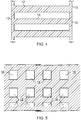
- Fig 3 illustrates a shield electrode 12 overlying, in the sensing area 8, conductive traces 10.
- the shield electrode 12 overlies at least portions of at least some of the sensor electrodes 6.
- the portions of the sensor electrodes 6 that are uncovered define operational sensor electrodes 6 of equal operational size, in this example.
- the sensor electrodes 6 are of similar construction they have the same capacitance per unit area. Therefore the operational sensor electrodes 6 of equal operational size have equal capacitance.
- the shield electrode 12 overlies, in the sensing area 8, all of the conductive traces 10. In other examples, the shield electrode 12 does not overlie, in the sensing area 8, all of the conductive traces 10 but instead overlies more than 80% of the area 14 occupied by the conductive traces 10.
- RC resistance-capacitance
- the shield electrode 12 may extends across the whole of the sensing area 8 as a strip 15.
- a strip may be associated with each row of capacitive sensor electrodes 6 (as illustrated in Fig 3 ).
- the shield electrode 12 may cover the whole of the sensing area 8 except at openings 18 through the shield electrode 18 to the underlying capacitive sensor electrodes 6.
- the openings 18 are of equal size.
- the openings 18 can be of any shape (for example, rectangle (as shown in the attached drawing), round, star etc.).
- the portions of the sensor electrodes 6 that are uncovered define operational sensor electrodes 6 of equal operational size. As the sensor electrodes 6 are of similar construction they have the same capacitance per unit area. Therefore the operational sensor electrodes 6 of equal operational size have equal capacitance.
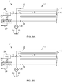
- Fig 6A schematically illustrates a cross-section through the sensing arrangement 5 along a line corresponding to an 'operational' capacitive sensor electrode. That is the shield electrode 12 along this cross-section does not cover the capacitive sensing electrodes 6.
- the portion of the shield electrode 12 illustrated is part of the guard portion 13.
- the portion of the shield electrode 12 illustrated may be part of a guard portion 13 adjacent a perimeter of the sensing area 8 or a portion between two adjacent openings 18 to adjacent capacitive sensing electrodes 6.
- Fig 6B schematically illustrates a cross-section through the sensing arrangement 5 along a line corresponding to where the shield electrode 12 is present in the sensing area 8. That is the shield electrode 12 along this cross-section does covers all or some of the conductive traces 10 and, optionally, some of the capacitive sensor electrode 12.
- the portion of the shield electrode 12 illustrated is part of the strip 15.
- the portion of the shield electrode 12 illustrated may be part of portion between two adjacent rows (or columns) of capacitive sensing electrodes 12.
- the sensor electrodes 6 and the conductive traces 10 may be arranged within a common plane 16. They may, for example, be formed by patterning a planar layer of transparent conductive material.
- the apparatus 2 may comprise circuitry as described below, however other circuitry is possible.
- Such circuitry may be configured to provide a voltage to the shield electrode 12. If the further shield electrode 20 is present, the same voltage may be provided to the shield electrode 12 and the further shield electrode 20.
- the provided voltage may be a fixed voltage or a time-varying voltage.
- One of many examples of a time varying voltage is an alternating sinusoidal voltage.
- the shield electrode 12 is operatively connected to a node 22.
- Operatively connected means that there is a signal path but they may or may not be directly physically connected.
- the node 22 is held at a constant potential such as, for example, ground potential.
- Circuitry 24 is configured to provide the constant potential. This could be a simple galvanic connection to ground provided by, for example, a housing, a ground plane or a chassis.
- a further shield electrode 20 is present. It is also operatively connected to the node 22.
- Detection circuitry 26 is operatively connected between the shield electrode 12 and the array 4 of capacitive sensor electrodes 6.
- a multiplexer 28 is operatively connected between the detection circuitry 26 and the array 4 of capacitive sensor electrodes 6.
- the multiplexer 28 is configured to isolate, for detection, each of the plurality of capacitive sensor electrodes 6 of the array 4.
- drive circuitry 30 is configured to provide a time-varying voltage to the shield electrode 12 and, if present, the further shield electrode 20.
- the time-varying voltage may be, for example, an alternating sinusoidal voltage.
- the drive circuitry 30 is thus configured to provide a time varying electric field at each of the sensor electrodes 6.
- the detection circuitry 26 is configured to detect a variation in capacitance arising from proximity of a user input device 32 to one or more of the plurality of sensor electrodes 6.
- the detection circuitry 26 may comprise a low-impedance charge amplifier.
- a capacitive current flows from the shielding electrode 12 through the detection circuitry 26 to one or more capacitive sensing electrodes 6.
- the charge amplifier in the detection circuitry 26 registers a charge displacement due to the current.
- the output of the charge amplifier may be rectified, for example synchronously rectified, and integrated, after which it is passed to an analog-to-digital converter and then provided as digital output 27 for processing in the digital domain.
- the drive voltage and the drive frequency typically range from 1 V to 10 V and from 10 to 200 kHz, respectively.
- a single charge amplifier and a single analog-to-digital converter may be used in the detection circuitry 26 for multiple capacitive sensing electrodes 6 and a multiplexer 28 may be used to isolate for sensing each capacitive sensing electrode 6 separately.
- Fig 7A illustrates a touch panel module 34 that comprise the apparatus 2.
- the touch panel module may be used in combination with a display to form a touch screen display.
- Fig 7B illustrates a touch sensitive display module 36 that comprises the apparatus 2 and a display 40.
- Fig 7C illustrates an electronic device 38 that comprises at least the apparatus 2. It may, for example, additionally comprise a processor 39 that processes the output 27 of the detection circuitry 26.
- module' refers to a unit or apparatus that excludes certain parts/components that would be added by an end manufacturer or a user.
Landscapes
- Engineering & Computer Science (AREA)
- General Engineering & Computer Science (AREA)
- Theoretical Computer Science (AREA)
- Human Computer Interaction (AREA)
- Physics & Mathematics (AREA)
- General Physics & Mathematics (AREA)
- Position Input By Displaying (AREA)
Claims (15)
- Appareil (2) comprenant :un réseau (4) d'électrodes de capteur capacitif (6) comprenant une pluralité d'électrodes de capteur capacitif distinctes distribuées sur une aire de détection (8) ;des traces conductrices (10) connectées à des électrodes respectives de la pluralité d'électrodes de capteur capacitif distinctes (6) ; etune électrode de protection (12) recouvrant les traces conductrices, l'électrode de protection s'étendant en travers de l'aire de détection en multiples bandes de protection parallèles, entre lesquelles sont définies des ouvertures à travers l'électrode de protection vers les électrodes de capteur capacitif sous-jacentes, les ouvertures définissant de multiples bandes non protégées parallèles ; etdans lequel l'électrode de protection (12) recouvre les traces conductrices (10) dans l'aire de détection (8).
- Appareil tel que revendiqué dans la revendication 1, dans lequel l'électrode de protection (12) recouvre, dans l'aire de détection (8), toutes les traces conductrices (10).
- Appareil tel que revendiqué dans une quelconque revendication précédente, dans lequel les électrodes de capteur (6) sont plus grandes vers une région centrale (8C) de l'aire de détection et plus petites vers un périmètre (8P) de l'aire de détection (8).
- Appareil tel que revendiqué dans une quelconque revendication précédente, dans lequel les électrodes de capteur (6) et les traces conductrices (10) sont agencées au sein d'un plan commun.
- Appareil tel que revendiqué dans une quelconque revendication précédente, dans lequel l'électrode de protection (12) recouvre au moins des parties d'au moins quelques-unes des électrodes de capteur (6).
- Appareil tel que revendiqué dans une quelconque revendication précédente, dans lequel l'électrode de protection (12) recouvre au moins des parties d'au moins quelques-unes des électrodes de capteur (6) afin de définir des électrodes de capteur opérationnelles d'une taille opérationnelle égale.
- Appareil tel que revendiqué dans une quelconque revendication précédente, dans lequel l'électrode de protection (12) recouvre au moins des parties d'au moins quelques-unes des électrodes de capteur (6) afin de définir des électrodes de capteur opérationnelles d'une capacitance opérationnelle égale.
- Appareil tel que revendiqué dans une quelconque revendication précédente, comprenant en outre une deuxième électrode de protection supplémentaire (20) sous-jacente, dans l'aire de détection (8), aux traces conductrices (10) et aux électrodes de détection (6).
- Appareil tel que revendiqué dans la revendication 8, dans lequel l'électrode de protection supplémentaire (20) est une électrode ininterrompue continue.
- Appareil tel que revendiqué dans la revendication 8 ou 9, dans lequel l'électrode de protection supplémentaire (20) est connectée de manière opérationnelle à un noeud (22), l'appareil (2) étant configuré pour maintenir le noeud (22) à un potentiel constant.
- Appareil tel que revendiqué dans n'importe lesquelles des revendications 1 à 10, comprenant des circuits (30) configurés pour fournir un signal de tension de référence variable dans le temps à l'électrode de protection.
- Appareil tel que revendiqué dans une quelconque revendication précédente, comprenant des circuits de détection (26) connectés entre l'électrode de protection (12) et le réseau (4) d'électrodes de capteur capacitif (6).
- Appareil tel que revendiqué dans une quelconque revendication précédente, comprenant des circuits de commande (30) configurés pour fournir un champ électrique variable dans le temps au niveau de chacune des électrodes de capteur et des circuits de détection (26) configurés pour détecter une variation en capacitance résultant de la proximité d'un dispositif de saisie d'utilisateur (32) par rapport à une ou plusieurs électrodes de la pluralité d'électrodes de capteur.
- Appareil tel que revendiqué dans la revendication 13, dans lequel les circuits de détection (26) sont configurés pour détecter une variation en capacitance résultant de la proximité d'un dispositif de saisie d'utilisateur (32) au niveau de ou au-dessus d'une surface tactile (7) de l'appareil (2).
- Panneau tactile capacitif pour un affichage (40) comprenant l'appareil tel que revendiqué dans n'importe lesquelles des revendications 1 à 14.
Applications Claiming Priority (2)
| Application Number | Priority Date | Filing Date | Title |
|---|---|---|---|
| US13/677,399 US9411474B2 (en) | 2012-11-15 | 2012-11-15 | Shield electrode overlying portions of capacitive sensor electrodes |
| PCT/FI2013/050914 WO2014076363A1 (fr) | 2012-11-15 | 2013-09-23 | Protection pour capteurs tactiles capacitifs |
Publications (3)
| Publication Number | Publication Date |
|---|---|
| EP2920677A1 EP2920677A1 (fr) | 2015-09-23 |
| EP2920677A4 EP2920677A4 (fr) | 2016-06-15 |
| EP2920677B1 true EP2920677B1 (fr) | 2019-10-23 |
Family
ID=50681142
Family Applications (1)
| Application Number | Title | Priority Date | Filing Date |
|---|---|---|---|
| EP13854578.5A Active EP2920677B1 (fr) | 2012-11-15 | 2013-09-23 | Protection pour capteurs tactiles capacitifs |
Country Status (6)
| Country | Link |
|---|---|
| US (1) | US9411474B2 (fr) |
| EP (1) | EP2920677B1 (fr) |
| KR (1) | KR101724978B1 (fr) |
| CN (1) | CN104781772B (fr) |
| TW (1) | TWI545486B (fr) |
| WO (1) | WO2014076363A1 (fr) |
Families Citing this family (44)
| Publication number | Priority date | Publication date | Assignee | Title |
|---|---|---|---|---|
| US8381135B2 (en) | 2004-07-30 | 2013-02-19 | Apple Inc. | Proximity detector in handheld device |
| US7920129B2 (en) | 2007-01-03 | 2011-04-05 | Apple Inc. | Double-sided touch-sensitive panel with shield and drive combined layer |
| FR2949007B1 (fr) | 2009-08-07 | 2012-06-08 | Nanotec Solution | Dispositif et procede d'interface de commande sensible a un mouvement d'un corps ou d'un objet et equipement de commande integrant ce dispositif. |
| FR2971066B1 (fr) | 2011-01-31 | 2013-08-23 | Nanotec Solution | Interface homme-machine tridimensionnelle. |
| FR2976688B1 (fr) | 2011-06-16 | 2021-04-23 | Nanotec Solution | Dispositif et procede pour generer une alimentation electrique dans un systeme electronique avec un potentiel de reference variable. |
| US9259904B2 (en) | 2011-10-20 | 2016-02-16 | Apple Inc. | Opaque thin film passivation |
| FR2985048B1 (fr) | 2011-12-21 | 2014-08-15 | Nanotec Solution | Dispositif et procede de mesure capacitive sensible a la pression pour interfaces tactiles et sans contact |
| FR2985049B1 (fr) | 2011-12-22 | 2014-01-31 | Nanotec Solution | Dispositif de mesure capacitive a electrodes commutees pour interfaces tactiles et sans contact |
| FR2988175B1 (fr) | 2012-03-13 | 2014-04-11 | Nanotec Solution | Procede de mesure capacitive par des electrodes non-regulieres, et appareil mettant en œuvre un tel procede |
| FR2988176B1 (fr) | 2012-03-13 | 2014-11-21 | Nanotec Solution | Procede de mesure capacitive entre un objet et un plan d’electrodes par demodulation synchrone partielle |
| TWI466003B (zh) * | 2012-12-26 | 2014-12-21 | Hannstouch Solution Inc | 觸控面板 |
| KR102023436B1 (ko) * | 2013-01-30 | 2019-09-20 | 엘지디스플레이 주식회사 | 터치 전극을 포함하는 디스플레이 장치 |
| FR3002052B1 (fr) | 2013-02-14 | 2016-12-09 | Fogale Nanotech | Procede et dispositif pour naviguer dans un ecran d'affichage et appareil comprenant une telle navigation |
| FR3003964B1 (fr) | 2013-04-02 | 2016-08-26 | Fogale Nanotech | Dispositif pour interagir, sans contact, avec un appareil electronique et/ou informatique, et appareil equipe d'un tel dispositif |
| FR3004551A1 (fr) | 2013-04-15 | 2014-10-17 | Fogale Nanotech | Procede de detection capacitif multizone, dispositif et appareil mettant en oeuvre le procede |
| FR3005763B1 (fr) | 2013-05-17 | 2016-10-14 | Fogale Nanotech | Dispositif et procede d'interface de commande capacitive adapte a la mise en œuvre d'electrodes de mesures fortement resistives |
| GB2518627A (en) * | 2013-09-25 | 2015-04-01 | Nokia Technologies Oy | An apparatus |
| FR3013472B1 (fr) | 2013-11-19 | 2016-07-08 | Fogale Nanotech | Dispositif accessoire couvrant pour un appareil portable electronique et/ou informatique, et appareil equipe d'un tel dispositif accessoire |
| FR3017723B1 (fr) | 2014-02-19 | 2017-07-21 | Fogale Nanotech | Procede d'interaction homme-machine par combinaison de commandes tactiles et sans contact |
| FR3019320B1 (fr) | 2014-03-28 | 2017-12-15 | Fogale Nanotech | Dispositif electronique de type montre-bracelet avec interface de commande sans contact et procede de controle d'un tel dispositif |
| CN106664088B (zh) | 2014-06-26 | 2021-02-05 | 密克罗奇普技术公司 | 电容式感测系统中目标对象耦合到馈入线路的补偿 |
| FR3025623B1 (fr) | 2014-09-05 | 2017-12-15 | Fogale Nanotech | Dispositif d'interface de commande et capteur d'empreintes digitales |
| FR3028061B1 (fr) | 2014-10-29 | 2016-12-30 | Fogale Nanotech | Dispositif capteur capacitif comprenant des electrodes ajourees |
| KR101637422B1 (ko) * | 2014-12-10 | 2016-07-08 | 주식회사 지2터치 | 터치 스크린 패널 |
| FR3032287B1 (fr) | 2015-02-04 | 2018-03-09 | Quickstep Technologies Llc | Dispositif de detection capacitif multicouches, et appareil comprenant le dispositif |
| KR102320639B1 (ko) * | 2015-02-04 | 2021-11-02 | 삼성디스플레이 주식회사 | 터치 스크린 패널 및 이의 제조 방법 |
| FR3033203B1 (fr) | 2015-02-27 | 2018-03-23 | Quickstep Technologies Llc | Procede pour interagir avec un appareil electronique et/ou informatique mettant en œuvre une surface de commande capacitive et une surface peripherique, interface et appareil mettant en œuvre ce procede |
| KR102335116B1 (ko) * | 2015-04-13 | 2021-12-03 | 삼성디스플레이 주식회사 | 터치 스크린 패널 및 이의 제조 방법 |
| US10186437B2 (en) * | 2015-10-05 | 2019-01-22 | Lam Research Corporation | Substrate holder having integrated temperature measurement electrical devices |
| US10429974B2 (en) | 2016-09-23 | 2019-10-01 | Apple Inc. | Touch sensor panel with top and/or bottom shielding |
| US10372282B2 (en) | 2016-12-01 | 2019-08-06 | Apple Inc. | Capacitive coupling reduction in touch sensor panels |
| KR102384229B1 (ko) | 2017-08-04 | 2022-04-07 | 삼성전자주식회사 | 지문인식가능 터치스크린 장치 및 그 동작방법 |
| US10521049B2 (en) * | 2017-09-29 | 2019-12-31 | Apple Inc. | Multi-via structures for touchscreens |
| US10622996B1 (en) | 2019-03-29 | 2020-04-14 | Industrial Technology Research Institute | Adjustable sensing capacitance microelectromechanical system (MEMS) apparatus |
| TWI705235B (zh) | 2019-07-19 | 2020-09-21 | 財團法人工業技術研究院 | 感測裝置 |
| US11531438B2 (en) | 2020-05-29 | 2022-12-20 | Apple Inc. | Differential drive and sense for touch sensor panel |
| KR102397356B1 (ko) * | 2021-03-10 | 2022-05-12 | 이성호 | 복수의 서로 다른 면적으로 구성된 검출부 및 이를 이용한 오브젝트 검출장치 |
| CN113050840B (zh) * | 2021-03-31 | 2024-05-17 | 京东方科技集团股份有限公司 | 触控基板、触控模组与显示装置 |
| KR20230006141A (ko) | 2021-07-02 | 2023-01-10 | 삼성전자주식회사 | 차폐 부재 및 차폐 부재를 포함하는 전자 장치 |
| KR102702978B1 (ko) | 2021-08-27 | 2024-09-05 | 주식회사 케이티앤지 | 에어로졸 생성 장치 |
| US12260045B2 (en) | 2021-09-24 | 2025-03-25 | Apple Inc. | Architecture for differential drive and sense for touch sensor panel |
| US11789561B2 (en) | 2021-09-24 | 2023-10-17 | Apple Inc. | Architecture for differential drive and sense touch technology |
| US12197679B2 (en) | 2022-05-06 | 2025-01-14 | Apple Inc. | Touch screen shield layer with ring and tapping points |
| JP2024169010A (ja) * | 2023-05-25 | 2024-12-05 | 株式会社ジャパンディスプレイ | センサモジュール、およびセンサモジュールを備えるセンサ装置と表示装置 |
Citations (1)
| Publication number | Priority date | Publication date | Assignee | Title |
|---|---|---|---|---|
| US20080002867A1 (en) * | 2000-06-09 | 2008-01-03 | Idex Asa | Sensor unit, especially for fingerprint sensors |
Family Cites Families (23)
| Publication number | Priority date | Publication date | Assignee | Title |
|---|---|---|---|---|
| US7663607B2 (en) * | 2004-05-06 | 2010-02-16 | Apple Inc. | Multipoint touchscreen |
| US6587093B1 (en) | 1999-11-04 | 2003-07-01 | Synaptics Incorporated | Capacitive mouse |
| US8054296B2 (en) * | 2007-01-03 | 2011-11-08 | Apple Inc. | Storing baseline information in EEPROM |
| WO2008104406A2 (fr) | 2007-03-01 | 2008-09-04 | Ident Technology Ag | Système d'électrodes servant à générer un signal indiquant la présence d'un objet à l'intérieur d'une zone d'observation |
| TW200844811A (en) | 2007-03-27 | 2008-11-16 | N trig ltd | Shield for a digitizer sensor |
| JP2009169720A (ja) | 2008-01-17 | 2009-07-30 | Smk Corp | タッチセンサ |
| US8629841B2 (en) * | 2008-04-30 | 2014-01-14 | Apple Inc. | Multi-touch sensor patterns and stack-ups |
| US8508495B2 (en) | 2008-07-03 | 2013-08-13 | Apple Inc. | Display with dual-function capacitive elements |
| US8217913B2 (en) * | 2009-02-02 | 2012-07-10 | Apple Inc. | Integrated touch screen |
| US7995041B2 (en) | 2009-02-02 | 2011-08-09 | Apple Inc. | Integrated touch screen |
| US20100201647A1 (en) * | 2009-02-11 | 2010-08-12 | Tpo Displays Corp. | Capacitive touch sensor |
| JP5337061B2 (ja) | 2009-02-20 | 2013-11-06 | セイコーインスツル株式会社 | タッチパネル及びこれを備える表示装置 |
| CN102334091B (zh) | 2009-02-26 | 2016-01-06 | 3M创新有限公司 | 触摸屏传感器和具有低可见度的覆盖微图案的图案化基材 |
| CN101907922B (zh) | 2009-06-04 | 2015-02-04 | 新励科技(深圳)有限公司 | 一种触感触控系统 |
| EP2300900B1 (fr) | 2009-06-24 | 2018-09-05 | Microchip Technology Germany GmbH | Agencement d'électrodes pour dispositif d'affichage |
| US9323398B2 (en) * | 2009-07-10 | 2016-04-26 | Apple Inc. | Touch and hover sensing |
| US9128545B2 (en) | 2010-05-14 | 2015-09-08 | Racing Optics, Inc. | Touch screen shield |
| JP2013526746A (ja) | 2010-05-14 | 2013-06-24 | イーロ・タッチ・ソリューションズ・インコーポレイテッド | タッチセンサ上のタッチの位置を検出するためのシステム及び方法 |
| US20110285661A1 (en) | 2010-05-18 | 2011-11-24 | Steven Porter Hotelling | Periphery Conductive Element for Touch Screen |
| KR20130108556A (ko) * | 2010-08-23 | 2013-10-04 | 사이프레스 세미컨덕터 코포레이션 | 컨패시턴스 스캐닝 근접성 검출 |
| US20120299868A1 (en) * | 2011-05-25 | 2012-11-29 | Broadcom Corporation | High Noise Immunity and High Spatial Resolution Mutual Capacitive Touch Panel |
| US8698769B2 (en) * | 2011-08-01 | 2014-04-15 | Sharp Kabushiki Kaisha | Dual mode capacitive touch panel |
| WO2013109698A1 (fr) * | 2012-01-17 | 2013-07-25 | Apple Inc. | Capteur d'empreinte digitale à circuiterie de détection de pixel pour coupler des électrodes et des rubans de détection de pixel, et procédé correspondant |
-
2012
- 2012-11-15 US US13/677,399 patent/US9411474B2/en not_active Expired - Fee Related
-
2013
- 2013-09-23 KR KR1020157015799A patent/KR101724978B1/ko not_active Expired - Fee Related
- 2013-09-23 CN CN201380059581.XA patent/CN104781772B/zh not_active Expired - Fee Related
- 2013-09-23 EP EP13854578.5A patent/EP2920677B1/fr active Active
- 2013-09-23 WO PCT/FI2013/050914 patent/WO2014076363A1/fr not_active Ceased
- 2013-11-14 TW TW102141444A patent/TWI545486B/zh not_active IP Right Cessation
Patent Citations (1)
| Publication number | Priority date | Publication date | Assignee | Title |
|---|---|---|---|---|
| US20080002867A1 (en) * | 2000-06-09 | 2008-01-03 | Idex Asa | Sensor unit, especially for fingerprint sensors |
Also Published As
| Publication number | Publication date |
|---|---|
| KR20150085041A (ko) | 2015-07-22 |
| EP2920677A4 (fr) | 2016-06-15 |
| TWI545486B (zh) | 2016-08-11 |
| CN104781772B (zh) | 2017-07-14 |
| US9411474B2 (en) | 2016-08-09 |
| TW201419111A (zh) | 2014-05-16 |
| EP2920677A1 (fr) | 2015-09-23 |
| KR101724978B1 (ko) | 2017-04-07 |
| CN104781772A (zh) | 2015-07-15 |
| US20140132335A1 (en) | 2014-05-15 |
| WO2014076363A1 (fr) | 2014-05-22 |
Similar Documents
| Publication | Publication Date | Title |
|---|---|---|
| US9411474B2 (en) | Shield electrode overlying portions of capacitive sensor electrodes | |
| EP3062201B1 (fr) | Dispositif d'entrée tactile | |
| CN114527893B (zh) | 具有顶部屏蔽和/或底部屏蔽的触摸传感器面板 | |
| US8829926B2 (en) | Transparent proximity sensor | |
| EP2951636B1 (fr) | Senseur capacitif intégré avec un dispositif d'affichage | |
| US20080238881A1 (en) | Shield for a digitizer sensor | |
| KR101681305B1 (ko) | 터치 입력 장치 | |
| US9958997B2 (en) | Adjustable shield electrode arrangement for capacitive touch sensor array | |
| US9110551B2 (en) | Capacitive sensor electrodes | |
| EP2920676B1 (fr) | Appareil de détection capacitif comprenant une matrice active sensible au toucher et des électrodes de blindage | |
| JP6133732B2 (ja) | 入力装置及びその検出方法 | |
| US20140043278A1 (en) | Electrode configuration for large touch screen | |
| EP2994816B1 (fr) | Réseau de capteurs tactiles et méthode correspondante | |
| US9417742B2 (en) | Touch sensitive display |
Legal Events
| Date | Code | Title | Description |
|---|---|---|---|
| PUAI | Public reference made under article 153(3) epc to a published international application that has entered the european phase |
Free format text: ORIGINAL CODE: 0009012 |
|
| 17P | Request for examination filed |
Effective date: 20150512 |
|
| AK | Designated contracting states |
Kind code of ref document: A1 Designated state(s): AL AT BE BG CH CY CZ DE DK EE ES FI FR GB GR HR HU IE IS IT LI LT LU LV MC MK MT NL NO PL PT RO RS SE SI SK SM TR |
|
| AX | Request for extension of the european patent |
Extension state: BA ME |
|
| DAX | Request for extension of the european patent (deleted) | ||
| RA4 | Supplementary search report drawn up and despatched (corrected) |
Effective date: 20160517 |
|
| RIC1 | Information provided on ipc code assigned before grant |
Ipc: G06F 3/041 20060101ALI20160510BHEP Ipc: G06F 3/047 20060101ALI20160510BHEP Ipc: G06F 3/044 20060101AFI20160510BHEP Ipc: H01L 23/522 20060101ALI20160510BHEP |
|
| STAA | Information on the status of an ep patent application or granted ep patent |
Free format text: STATUS: EXAMINATION IS IN PROGRESS |
|
| 17Q | First examination report despatched |
Effective date: 20180320 |
|
| GRAP | Despatch of communication of intention to grant a patent |
Free format text: ORIGINAL CODE: EPIDOSNIGR1 |
|
| STAA | Information on the status of an ep patent application or granted ep patent |
Free format text: STATUS: GRANT OF PATENT IS INTENDED |
|
| INTG | Intention to grant announced |
Effective date: 20190515 |
|
| RAP1 | Party data changed (applicant data changed or rights of an application transferred) |
Owner name: NOKIA TECHNOLOGIES OY |
|
| GRAS | Grant fee paid |
Free format text: ORIGINAL CODE: EPIDOSNIGR3 |
|
| GRAA | (expected) grant |
Free format text: ORIGINAL CODE: 0009210 |
|
| STAA | Information on the status of an ep patent application or granted ep patent |
Free format text: STATUS: THE PATENT HAS BEEN GRANTED |
|
| AK | Designated contracting states |
Kind code of ref document: B1 Designated state(s): AL AT BE BG CH CY CZ DE DK EE ES FI FR GB GR HR HU IE IS IT LI LT LU LV MC MK MT NL NO PL PT RO RS SE SI SK SM TR |
|
| REG | Reference to a national code |
Ref country code: GB Ref legal event code: FG4D |
|
| REG | Reference to a national code |
Ref country code: CH Ref legal event code: EP |
|
| REG | Reference to a national code |
Ref country code: IE Ref legal event code: FG4D |
|
| REG | Reference to a national code |
Ref country code: DE Ref legal event code: R096 Ref document number: 602013062106 Country of ref document: DE |
|
| REG | Reference to a national code |
Ref country code: AT Ref legal event code: REF Ref document number: 1194403 Country of ref document: AT Kind code of ref document: T Effective date: 20191115 |
|
| REG | Reference to a national code |
Ref country code: NL Ref legal event code: MP Effective date: 20191023 |
|
| REG | Reference to a national code |
Ref country code: LT Ref legal event code: MG4D |
|
| PG25 | Lapsed in a contracting state [announced via postgrant information from national office to epo] |
Ref country code: ES Free format text: LAPSE BECAUSE OF FAILURE TO SUBMIT A TRANSLATION OF THE DESCRIPTION OR TO PAY THE FEE WITHIN THE PRESCRIBED TIME-LIMIT Effective date: 20191023 Ref country code: LV Free format text: LAPSE BECAUSE OF FAILURE TO SUBMIT A TRANSLATION OF THE DESCRIPTION OR TO PAY THE FEE WITHIN THE PRESCRIBED TIME-LIMIT Effective date: 20191023 Ref country code: SE Free format text: LAPSE BECAUSE OF FAILURE TO SUBMIT A TRANSLATION OF THE DESCRIPTION OR TO PAY THE FEE WITHIN THE PRESCRIBED TIME-LIMIT Effective date: 20191023 Ref country code: NO Free format text: LAPSE BECAUSE OF FAILURE TO SUBMIT A TRANSLATION OF THE DESCRIPTION OR TO PAY THE FEE WITHIN THE PRESCRIBED TIME-LIMIT Effective date: 20200123 Ref country code: PL Free format text: LAPSE BECAUSE OF FAILURE TO SUBMIT A TRANSLATION OF THE DESCRIPTION OR TO PAY THE FEE WITHIN THE PRESCRIBED TIME-LIMIT Effective date: 20191023 Ref country code: GR Free format text: LAPSE BECAUSE OF FAILURE TO SUBMIT A TRANSLATION OF THE DESCRIPTION OR TO PAY THE FEE WITHIN THE PRESCRIBED TIME-LIMIT Effective date: 20200124 Ref country code: BG Free format text: LAPSE BECAUSE OF FAILURE TO SUBMIT A TRANSLATION OF THE DESCRIPTION OR TO PAY THE FEE WITHIN THE PRESCRIBED TIME-LIMIT Effective date: 20200123 Ref country code: NL Free format text: LAPSE BECAUSE OF FAILURE TO SUBMIT A TRANSLATION OF THE DESCRIPTION OR TO PAY THE FEE WITHIN THE PRESCRIBED TIME-LIMIT Effective date: 20191023 Ref country code: LT Free format text: LAPSE BECAUSE OF FAILURE TO SUBMIT A TRANSLATION OF THE DESCRIPTION OR TO PAY THE FEE WITHIN THE PRESCRIBED TIME-LIMIT Effective date: 20191023 Ref country code: FI Free format text: LAPSE BECAUSE OF FAILURE TO SUBMIT A TRANSLATION OF THE DESCRIPTION OR TO PAY THE FEE WITHIN THE PRESCRIBED TIME-LIMIT Effective date: 20191023 Ref country code: PT Free format text: LAPSE BECAUSE OF FAILURE TO SUBMIT A TRANSLATION OF THE DESCRIPTION OR TO PAY THE FEE WITHIN THE PRESCRIBED TIME-LIMIT Effective date: 20200224 |
|
| PG25 | Lapsed in a contracting state [announced via postgrant information from national office to epo] |
Ref country code: HR Free format text: LAPSE BECAUSE OF FAILURE TO SUBMIT A TRANSLATION OF THE DESCRIPTION OR TO PAY THE FEE WITHIN THE PRESCRIBED TIME-LIMIT Effective date: 20191023 Ref country code: RS Free format text: LAPSE BECAUSE OF FAILURE TO SUBMIT A TRANSLATION OF THE DESCRIPTION OR TO PAY THE FEE WITHIN THE PRESCRIBED TIME-LIMIT Effective date: 20191023 Ref country code: IS Free format text: LAPSE BECAUSE OF FAILURE TO SUBMIT A TRANSLATION OF THE DESCRIPTION OR TO PAY THE FEE WITHIN THE PRESCRIBED TIME-LIMIT Effective date: 20200224 |
|
| PG25 | Lapsed in a contracting state [announced via postgrant information from national office to epo] |
Ref country code: AL Free format text: LAPSE BECAUSE OF FAILURE TO SUBMIT A TRANSLATION OF THE DESCRIPTION OR TO PAY THE FEE WITHIN THE PRESCRIBED TIME-LIMIT Effective date: 20191023 |
|
| REG | Reference to a national code |
Ref country code: DE Ref legal event code: R097 Ref document number: 602013062106 Country of ref document: DE |
|
| PG2D | Information on lapse in contracting state deleted |
Ref country code: IS |
|
| PG25 | Lapsed in a contracting state [announced via postgrant information from national office to epo] |
Ref country code: EE Free format text: LAPSE BECAUSE OF FAILURE TO SUBMIT A TRANSLATION OF THE DESCRIPTION OR TO PAY THE FEE WITHIN THE PRESCRIBED TIME-LIMIT Effective date: 20191023 Ref country code: DK Free format text: LAPSE BECAUSE OF FAILURE TO SUBMIT A TRANSLATION OF THE DESCRIPTION OR TO PAY THE FEE WITHIN THE PRESCRIBED TIME-LIMIT Effective date: 20191023 Ref country code: RO Free format text: LAPSE BECAUSE OF FAILURE TO SUBMIT A TRANSLATION OF THE DESCRIPTION OR TO PAY THE FEE WITHIN THE PRESCRIBED TIME-LIMIT Effective date: 20191023 Ref country code: CZ Free format text: LAPSE BECAUSE OF FAILURE TO SUBMIT A TRANSLATION OF THE DESCRIPTION OR TO PAY THE FEE WITHIN THE PRESCRIBED TIME-LIMIT Effective date: 20191023 Ref country code: IS Free format text: LAPSE BECAUSE OF FAILURE TO SUBMIT A TRANSLATION OF THE DESCRIPTION OR TO PAY THE FEE WITHIN THE PRESCRIBED TIME-LIMIT Effective date: 20200223 |
|
| REG | Reference to a national code |
Ref country code: AT Ref legal event code: MK05 Ref document number: 1194403 Country of ref document: AT Kind code of ref document: T Effective date: 20191023 |
|
| PLBE | No opposition filed within time limit |
Free format text: ORIGINAL CODE: 0009261 |
|
| STAA | Information on the status of an ep patent application or granted ep patent |
Free format text: STATUS: NO OPPOSITION FILED WITHIN TIME LIMIT |
|
| PG25 | Lapsed in a contracting state [announced via postgrant information from national office to epo] |
Ref country code: SM Free format text: LAPSE BECAUSE OF FAILURE TO SUBMIT A TRANSLATION OF THE DESCRIPTION OR TO PAY THE FEE WITHIN THE PRESCRIBED TIME-LIMIT Effective date: 20191023 Ref country code: IT Free format text: LAPSE BECAUSE OF FAILURE TO SUBMIT A TRANSLATION OF THE DESCRIPTION OR TO PAY THE FEE WITHIN THE PRESCRIBED TIME-LIMIT Effective date: 20191023 Ref country code: SK Free format text: LAPSE BECAUSE OF FAILURE TO SUBMIT A TRANSLATION OF THE DESCRIPTION OR TO PAY THE FEE WITHIN THE PRESCRIBED TIME-LIMIT Effective date: 20191023 |
|
| 26N | No opposition filed |
Effective date: 20200724 |
|
| PGFP | Annual fee paid to national office [announced via postgrant information from national office to epo] |
Ref country code: DE Payment date: 20200909 Year of fee payment: 8 |
|
| PG25 | Lapsed in a contracting state [announced via postgrant information from national office to epo] |
Ref country code: AT Free format text: LAPSE BECAUSE OF FAILURE TO SUBMIT A TRANSLATION OF THE DESCRIPTION OR TO PAY THE FEE WITHIN THE PRESCRIBED TIME-LIMIT Effective date: 20191023 Ref country code: SI Free format text: LAPSE BECAUSE OF FAILURE TO SUBMIT A TRANSLATION OF THE DESCRIPTION OR TO PAY THE FEE WITHIN THE PRESCRIBED TIME-LIMIT Effective date: 20191023 |
|
| PG25 | Lapsed in a contracting state [announced via postgrant information from national office to epo] |
Ref country code: MC Free format text: LAPSE BECAUSE OF FAILURE TO SUBMIT A TRANSLATION OF THE DESCRIPTION OR TO PAY THE FEE WITHIN THE PRESCRIBED TIME-LIMIT Effective date: 20191023 |
|
| REG | Reference to a national code |
Ref country code: CH Ref legal event code: PL |
|
| GBPC | Gb: european patent ceased through non-payment of renewal fee |
Effective date: 20200923 |
|
| REG | Reference to a national code |
Ref country code: BE Ref legal event code: MM Effective date: 20200930 |
|
| PG25 | Lapsed in a contracting state [announced via postgrant information from national office to epo] |
Ref country code: LU Free format text: LAPSE BECAUSE OF NON-PAYMENT OF DUE FEES Effective date: 20200923 |
|
| PG25 | Lapsed in a contracting state [announced via postgrant information from national office to epo] |
Ref country code: FR Free format text: LAPSE BECAUSE OF NON-PAYMENT OF DUE FEES Effective date: 20200930 |
|
| PG25 | Lapsed in a contracting state [announced via postgrant information from national office to epo] |
Ref country code: CH Free format text: LAPSE BECAUSE OF NON-PAYMENT OF DUE FEES Effective date: 20200930 Ref country code: BE Free format text: LAPSE BECAUSE OF NON-PAYMENT OF DUE FEES Effective date: 20200930 Ref country code: GB Free format text: LAPSE BECAUSE OF NON-PAYMENT OF DUE FEES Effective date: 20200923 Ref country code: IE Free format text: LAPSE BECAUSE OF NON-PAYMENT OF DUE FEES Effective date: 20200923 Ref country code: LI Free format text: LAPSE BECAUSE OF NON-PAYMENT OF DUE FEES Effective date: 20200930 |
|
| REG | Reference to a national code |
Ref country code: DE Ref legal event code: R119 Ref document number: 602013062106 Country of ref document: DE |
|
| PG25 | Lapsed in a contracting state [announced via postgrant information from national office to epo] |
Ref country code: TR Free format text: LAPSE BECAUSE OF FAILURE TO SUBMIT A TRANSLATION OF THE DESCRIPTION OR TO PAY THE FEE WITHIN THE PRESCRIBED TIME-LIMIT Effective date: 20191023 Ref country code: MT Free format text: LAPSE BECAUSE OF FAILURE TO SUBMIT A TRANSLATION OF THE DESCRIPTION OR TO PAY THE FEE WITHIN THE PRESCRIBED TIME-LIMIT Effective date: 20191023 Ref country code: CY Free format text: LAPSE BECAUSE OF FAILURE TO SUBMIT A TRANSLATION OF THE DESCRIPTION OR TO PAY THE FEE WITHIN THE PRESCRIBED TIME-LIMIT Effective date: 20191023 |
|
| PG25 | Lapsed in a contracting state [announced via postgrant information from national office to epo] |
Ref country code: MK Free format text: LAPSE BECAUSE OF FAILURE TO SUBMIT A TRANSLATION OF THE DESCRIPTION OR TO PAY THE FEE WITHIN THE PRESCRIBED TIME-LIMIT Effective date: 20191023 |
|
| PG25 | Lapsed in a contracting state [announced via postgrant information from national office to epo] |
Ref country code: DE Free format text: LAPSE BECAUSE OF NON-PAYMENT OF DUE FEES Effective date: 20220401 |