EP2921959A1 - Procédé et agencement de correction efficace d'erreurs à un seul bit - Google Patents
Procédé et agencement de correction efficace d'erreurs à un seul bit Download PDFInfo
- Publication number
- EP2921959A1 EP2921959A1 EP14160521.2A EP14160521A EP2921959A1 EP 2921959 A1 EP2921959 A1 EP 2921959A1 EP 14160521 A EP14160521 A EP 14160521A EP 2921959 A1 EP2921959 A1 EP 2921959A1
- Authority
- EP
- European Patent Office
- Prior art keywords
- memory unit
- memory
- unit
- control logic
- access control
- Prior art date
- Legal status (The legal status is an assumption and is not a legal conclusion. Google has not performed a legal analysis and makes no representation as to the accuracy of the status listed.)
- Withdrawn
Links
Images
Classifications
-
- G—PHYSICS
- G06—COMPUTING OR CALCULATING; COUNTING
- G06F—ELECTRIC DIGITAL DATA PROCESSING
- G06F11/00—Error detection; Error correction; Monitoring
- G06F11/07—Responding to the occurrence of a fault, e.g. fault tolerance
- G06F11/08—Error detection or correction by redundancy in data representation, e.g. by using checking codes
- G06F11/10—Adding special bits or symbols to the coded information, e.g. parity check, casting out 9's or 11's
- G06F11/1008—Adding special bits or symbols to the coded information, e.g. parity check, casting out 9's or 11's in individual solid state devices
- G06F11/1048—Adding special bits or symbols to the coded information, e.g. parity check, casting out 9's or 11's in individual solid state devices using arrangements adapted for a specific error detection or correction feature
Definitions
- the present invention relates generally to the field of electronic and logic circuits.
- the present invention relates to a method for efficiently correcting one-bit errors in a memory unit and to an associated arrangement for carrying out the method according to the invention.
- at least one memory unit is provided in which data units are stored by means of write accesses and from which data units can be read out by means of read accesses.
- an error correction module is provided for this memory unit with which one-bit errors in the memory unit are detected and corrected.
- Logical or electronic circuits today form the basis for all electronics, especially in computer technology.
- memory units For storing and storing data units which are used or generated by components of the electronic circuit for carrying out processes or procedures, memory units, so-called electronic memory modules, are usually provided.
- a memory unit or memory module is an integrated circuit, which consists of a plurality of memory cells for the storage of data units.
- Memory devices are described, for example, as so-called Random Access Memory (RAM), EPROM or as so-called flash memory, e.g. offered for soldering on a circuit board.
- RAM Random Access Memory
- EPROM EPROM
- flash memory e.g. offered for soldering on a circuit board.
- a RAM is, for example, a random access memory in which information or data units are stored get saved.
- RAMs are realized, for example, as an integrated circuit mainly in silicon technology and used in all types of electronic devices or circuits (eg as a working memory in a computer, etc.).
- RAMs such as so-called volatile or volatile RAMs, which are most commonly used, and so-called nonvolatile RAMs (eg magnetic or ferromagnetic RAMs, resistive RAMs), which represent a very new and recent development.
- volatile or volatile RAMs eg magnetic or ferromagnetic RAMs, resistive RAMs
- Such a volatile RAM is the so-called static RAM or SRAM besides the frequently used dynamic RAM.
- SRAMs are used as fast memories with relatively small data capacity, for example everywhere where data contents must be accessed quickly eg by means of read and / or write accesses, eg in processors as so-called cache or in electronic integrated circuits (eg ASICs, FPGAs, etc.). ) as local memory on a chip.
- SER soft error rate
- one, two or more bits of a stored data unit eg a data word
- a one-bit error, two-bit error or multiple-bit error e.g., a one-bit error or bit error is an error in a single bit of a stored data unit. Instead of the correct value (ie the value 0 or 1), this bit has the other value - ie instead of a 1, a 0 or vice versa is filed.
- Such a bit is then called tilted or upset.
- Such a bit is then called tilted or upset.
- Such one-bit errors in data units can be detected, for example by means of a so-called parity bit, but not corrected.
- To correct a one-bit error usually more complex procedures with so-called error-correcting codes such as the so-called Error Correcting Code (ECC) are required.
- ECC Error Correcting Code
- Error correcting code or ECC is an error correction method for memory units in which redundant information (eg so-called check bits) are generated and stored with the corresponding, associated data unit in the memory unit. With this redundant information, for example, one-bit errors during read accesses to the respective data unit stored in the memory unit can then be detected and corrected, and two-bit and sometimes also multi-bit errors can be detected.
- redundant information eg so-called check bits
- a memory controller by which a data flow between an accessing unit (eg processor, CPU, etc.) and the memory unit is controlled, to master, for example, a corresponding ECC algorithm.
- the memory controller is thereby expanded in some way to an error correction module.
- the error correction module extended memory controller is then checked, for example, based on the stored in the data units check bits during read access to these data units or to the memory unit, whether the respective data units have changed. For example, if a one-bit error is detected in a data unit read from the memory unit, this one-bit error in the read data unit is corrected. However, no correction of the data unit in the memory unit is performed - ie corrected data units are not written back to the memory unit. Thus, for example, until the data unit is overwritten, the one-bit error remains in the memory unit and it can become a result possibly an uncorrectable two or more bit error.
- a disadvantage of such a method is that write accesses, with which the corrected data units are written back to the memory unit, correspond to the read accesses of accessing units (eg Processor, CPU, etc.) or other write accesses in order to avoid access conflicts
- accessing units eg Processor, CPU, etc.
- such a method requires a specific adaptation of an external interface of the memory unit (eg HOLD mechanism for inserting a wait state or waitstates for an interruption) of the respective current access Ne surrounding electronic circuit can be adjusted.
- HOLD mechanism for inserting a wait state or waitstates for an interruption
- the arbitration and / or the use of a HOLD mechanism for example, substantially reduces performance or the speed of accessing the memory unit.
- the invention is therefore based on the object of specifying a method and an arrangement for carrying out the method, by which in a simple manner without additional effort One-bit error can be corrected without performance losses.
- the object is achieved by a method of the kind mentioned in the opening paragraph, in which a first memory unit with error correction module for e.g. an electronic circuit is supplemented by a second memory unit with associated access control logic.
- the error correction module of the first memory unit is coupled to the access control logic of the second memory unit.
- a read access of a unit of the electronic circuit eg CPU, processor, etc.
- the main aspect of the method proposed according to the invention is that no arbitration of accesses to the first memory unit is necessary by the second memory unit with access control logic for corrected data units. Therefore, with consistent system availability, the performance of accesses, such as CPUs, processors, etc. of an electronic circuit is not lowered. Due to the possibility of simultaneous reading from the first storage unit and writing to the second storage unit, the access performance remains largely the same as without the inventive method. Furthermore, when using the method according to the invention, no adaptation of an external interface of the first memory unit is necessary.
- the method according to the invention can also be simple in already existing electronic circuits are integrated - it is only a second memory unit with associated access control logic to complete.
- a first memory address of the erroneous and corrected data unit in the first memory unit and a second memory address of this data unit is stored in the second memory unit of the access control logic in an associated address table.
- a redirection to the second memory address in the second memory unit is performed, at which the correspondingly corrected data unit is stored.
- the write access to the first memory address at which a faulty data unit has been detected, the corresponding second memory address in the second memory unit via the access control logic using the associated address table is set to invalid.
- a second memory address in the second memory unit is released again in a simple manner if the faulty data unit is overwritten by new data at the corresponding first memory address in the first memory unit.
- a subsequent read access to the first memory address is then accessed again to the first memory unit and checked whether the data unit stored therein has a one-bit error or not.
- a size of the second memory unit which may be listed as a so-called static Ramdom Access Memory (SRAM) or as a register memory, for example, is measured at a probability with which one-bit errors are converted into so-called two-bit errors become.
- SRAM static Ramdom Access Memory
- the size of the second memory unit can be adapted to the corresponding memory requirements.
- the cost - especially when using an SRAM which requires, for example, more devices (e.g., transistors, etc.) and chip area than other memory devices such as memory devices, can be reduced.
- a dynamic RAM, etc. - are kept as low as possible.
- a register memory or a register bank may be used instead of an SRAM for the second memory unit.
- a register memory is a number of registers organized in blocks and then individually accessed via the access control logic as e.g. Address decoder can be controlled. For speed reasons, the registers of the register memory may be e.g. be addressed via direct control lines.
- This arrangement consists of at least a first memory unit for storing data units (eg for use, processing, etc. in an electronic circuit) with an associated error correction module, of which in particular one-bit error detected and corrected and optionally two-bit errors are detected can. Furthermore, in the arrangement according to the invention, a second memory unit with an associated access control logic, which is coupled to the error correction module of the first memory unit, provided such that in a detected one-bit error in a stored in the first memory unit data unit corrected by the error correction module data unit is written to the second storage unit using the access control logic.
- the advantages that can be achieved with the switching arrangement according to the invention are, in particular, that by supplementing the second memory unit and the associated access control logic with a correction of one-bit errors, a system availability of an associated electronic circuit remains the same, since one-bit errors are detected and corrected. Furthermore, the corrected data units are available for further read access in the second memory unit, so that, for example, no further correction of a one-bit-errored data unit from the first memory unit is necessary, if it has already been performed once.
- the use of the second memory unit with the associated access control logic prevents performance losses in reading accesses to the first memory unit, since the second memory unit used in the arrangement according to the invention enables parallel reading / checking / correction of data units from the first memory unit and writing from corrected data units to the second storage unit is possible.
- the inventive arrangement is also in a simple manner and without adjustments (eg, an external interface of the first memory unit) in electronic circuits can be used or integrated without modification of a surrounding circuit in existing electronic circuits.
- the access control logic of the second memory unit comprises at least one address table.
- this address table memory addresses of data units of the first memory unit are linked to memory addresses of the second memory unit and stored. Through the address table corrected data can be found quickly and easily in the second memory unit after a correction of one-bit errors during read accesses and then made available to an accessing unit of an electronic circuit.
- the address table can also be used to determine in an efficient manner whether corrected data is available for a memory address of the first memory unit.
- the access control logic of the second memory unit has a comparison unit for comparing memory addresses.
- This comparison unit is ideally used in a read access and / or write access to a first memory address of the first memory unit in order to determine in a simple and rapid manner whether it is linked to a second memory address of the second memory unit via the address table. In this way, a corrected data unit stored in the second storage unit can be found very quickly and simply during a read access. Access to the first storage unit is therefore no longer necessary.
- a second memory address possibly associated with the first memory address can be quickly found in the second memory unit and set to invalid.
- the access control logic of the second memory unit also includes an error correction module so that single-bit errors occurring in the second memory unit can be easily detected and corrected.
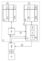
- FIG. 1 shows, in an exemplary and schematic manner, an arrangement for carrying out a method for the efficient correction of one-bit errors as well as a sequence of the method according to the invention.
- Figure 1 shows, in a schematic and exemplary manner, an arrangement AN for carrying out the method according to the invention for the efficient correction of one-bit errors.
- the arrangement AN according to the invention comprises at least a first memory unit SP1, such as e.g. a static random access memory as well as an error correction module FM belonging to the first memory unit SP1, which e.g. can be implemented as Error Correcting Code or ECC logic.
- a first memory unit SP1 such as e.g. a static random access memory
- an error correction module FM belonging to the first memory unit SP1
- ECC logic Error Correcting Code
- data units are stored at memory addresses SA11 to SA1N.
- the data units are secured by so-called backup or check or ECC bits E11 to EIN, which are stored in the data units or associated memory addresses SA11 to SA1N.
- ECC logic is used as the error correction module FM
- redundant information is generated, for example, when a data unit is stored at a first memory address SA11 in the first memory unit SP1 and stored as ECC bits E11 at the first memory address SA11.
- the ECC bits E11 can then be used by the error correction module FM for a read access to the first memory address SA11 to check whether the data unit stored therein has a one-bit error.
- This one-bit error can then be corrected by the error correction module FM using the ECC bits E11.
- the aid of the ECC bits E11 to ON two-bit and / or multi-bit errors in the associated data units can be detected by the error correction module FM.
- the arrangement AN according to the invention further comprises a second storage unit SP2, which e.g. can be implemented as SRAM or as a register memory or register file.
- a second storage unit SP2 which e.g. can be implemented as SRAM or as a register memory or register file.
- data units can likewise be stored at memory addresses SA21 to SA2M.
- the data units stored in the second memory unit SP2 can also be protected by so-called backup or check or ECC bits E21 to E2M, which are stored in the data units or associated memory addresses SA21 to SA2M.
- an access control logic ZS which belongs to the second memory unit SP2 and from which read and write accesses to the second memory unit SP2 are regulated.
- the access control logic comprises at least one address table AT, a comparison unit VE and an error correction module FMZ for the second memory unit SP2.
- the memory addresses SA11 to SA1N of the first memory unit SP1 can be linked to memory addresses SA21 to SA2M of the second memory unit SP2.
- the comparison unit VE can then derive from the access control logic e.g. a read or write access coming from units SE (e.g., CPU, processor, etc.) of a surrounding electronic circuit, an access address is compared with the memory addresses SA11 to SA1N of the first memory unit SP1 stored in the address table AT.
- the access control logic ZS of the second memory unit SP2 is coupled to the error correction module FM of the first memory unit, so that, for example, corrected data units, information via memory addresses SA11 to SA1N of the first memory unit SP1, etc. can be forwarded to the access control logic ZS for processing.
- the inventive arrangement AN in particular at least at the error correction module FM and the access control logic ZS interfaces to a surrounding electronic circuit, for example via a multiplexer MUX.
- the multiplexer MUX can be used to read and / or write the device AN and the associated memory units SP1, SP2 from units SE such as CPU, processor, etc. of the surrounding electronic circuit.
- the first memory unit SP1 with error correction module FM in which data units with check or ECC bits E11 to ON are stored at memory addresses SA11 to SA1N, supplemented by the second memory unit SP2 with associated access control logic ZS.
- the access control logic ZS of the second memory unit SP2 is coupled to the error correction module FM of the first memory unit SP1.
- a one-bit error in this data unit is detected by the error correction module FM during a read access to a data unit stored in a first memory address SA11 in the first memory unit SP1 on the basis of the associated check or ECC bits E11, then in a third method step 3 One-bit error in this data unit corrected by the error correction module FM.
- the corrected data unit is then forwarded, for example, to the accessing unit SE of the surrounding unit.
- the corrected data unit with the first memory address SA11, at which it is stored in the first memory unit SP1 is forwarded to the access control logic ZS of the second memory unit.
- the corrected data unit is then in a fourth method step 4 using the access control logic ZS at a second memory address SA21 in the stored second memory unit SP2.
- This second memory address SA21 is entered by the access control logic with the first memory address SA11 of the data unit in the first memory unit SP1 in the address table AT. Furthermore, check or ECC bits E21 can be determined by the error correction module FMZ of the access control logic for the corrected data unit and stored with the data unit at the second memory address SA21 in the memory unit SP2.
- a unit SE of the surrounding electronic circuit is accessed by read access to the data unit in the first memory address SA11 of the first memory unit SP1, this read access is sent via the multiplexer MUX to the error correction module FM and to the access control logic ZS sent.
- the access control logic ZS it is determined by the access control logic ZS with the aid of the comparison unit VE on the basis of the address table AT that a corrected data unit exists in the second memory unit SP2 for the first memory address SA11.
- the read access to the first memory unit SP1 is thereby prevented and redirected from the access control logic ZS to the second memory unit SP2.
- the access control logic ZS uses the address table AT to determine the second memory address SA21 of the corrected data unit in the second memory unit SP2.
- the corrected data unit is then read from the second memory unit SP2, optionally checked and corrected with the error correction module FMZ, and transmitted by the access control logic ZS via the multiplexer MUX to the accessing unit SE of the surrounding electronic circuit.
- a unit SE of the surrounding electronic circuit writes to the first memory address SA11 of the first memory unit SP1, at which a one-bit error has been detected. So this will be write access via the multiplexer MUX again passed to the error correction module FM of the first memory unit SP1 and to the access control logic ZS for the second memory unit SP2.
- the access control logic ZS recognizes the write access and determines from the address table AT with the aid of the comparison unit VE that a corrected data unit is stored at the second memory address SA21 in the second memory unit SP2 for the first memory address SA11 in the first memory unit SP1.
- the second memory address SA21 in the second memory unit SP2 is then set to invalid, for example by means of the address table AT, so that upon a renewed read access to the first memory address SA11 of the first memory unit SP1, no redirection to the second memory unit SP2 is performed.
- the data at the first memory address SA11 in the first memory unit SP1 are overwritten by a new data unit or by the write access. From the fault module FM of the first memory unit SP1 corresponding check or ECC bits E11 can be created for the newly entered data unit and entered with the new data unit at the first memory address SA11.
- correspondingly corrected data units without one-bit error for reading accesses are provided by the second memory unit SP2 for data units which are defective in the first memory unit SP1.
- one-bit-error data units are not corrected.
- the size of the second memory unit SP2 is ideally estimated by a probability with which one-bit errors are converted into two-bit errors.
Landscapes
- Engineering & Computer Science (AREA)
- Theoretical Computer Science (AREA)
- Quality & Reliability (AREA)
- Physics & Mathematics (AREA)
- General Engineering & Computer Science (AREA)
- General Physics & Mathematics (AREA)
- Techniques For Improving Reliability Of Storages (AREA)
- For Increasing The Reliability Of Semiconductor Memories (AREA)
Priority Applications (1)
| Application Number | Priority Date | Filing Date | Title |
|---|---|---|---|
| EP14160521.2A EP2921959A1 (fr) | 2014-03-18 | 2014-03-18 | Procédé et agencement de correction efficace d'erreurs à un seul bit |
Applications Claiming Priority (1)
| Application Number | Priority Date | Filing Date | Title |
|---|---|---|---|
| EP14160521.2A EP2921959A1 (fr) | 2014-03-18 | 2014-03-18 | Procédé et agencement de correction efficace d'erreurs à un seul bit |
Publications (1)
| Publication Number | Publication Date |
|---|---|
| EP2921959A1 true EP2921959A1 (fr) | 2015-09-23 |
Family
ID=50486741
Family Applications (1)
| Application Number | Title | Priority Date | Filing Date |
|---|---|---|---|
| EP14160521.2A Withdrawn EP2921959A1 (fr) | 2014-03-18 | 2014-03-18 | Procédé et agencement de correction efficace d'erreurs à un seul bit |
Country Status (1)
| Country | Link |
|---|---|
| EP (1) | EP2921959A1 (fr) |
Cited By (1)
| Publication number | Priority date | Publication date | Assignee | Title |
|---|---|---|---|---|
| WO2017105757A1 (fr) * | 2015-12-15 | 2017-06-22 | Qualcomm Incorporated | Systèmes, procédés et programmes informatiques pour résoudre les défauts de dram |
Citations (2)
| Publication number | Priority date | Publication date | Assignee | Title |
|---|---|---|---|---|
| US4939694A (en) * | 1986-11-03 | 1990-07-03 | Hewlett-Packard Company | Defect tolerant self-testing self-repairing memory system |
| US20080133994A1 (en) * | 2006-12-05 | 2008-06-05 | Jong-Hoon Oh | Error correction in memory devices |
-
2014
- 2014-03-18 EP EP14160521.2A patent/EP2921959A1/fr not_active Withdrawn
Patent Citations (2)
| Publication number | Priority date | Publication date | Assignee | Title |
|---|---|---|---|---|
| US4939694A (en) * | 1986-11-03 | 1990-07-03 | Hewlett-Packard Company | Defect tolerant self-testing self-repairing memory system |
| US20080133994A1 (en) * | 2006-12-05 | 2008-06-05 | Jong-Hoon Oh | Error correction in memory devices |
Non-Patent Citations (1)
| Title |
|---|
| C.-L. SU; Y.-T. YEH; C.-W. WU: "An Integrated ECC and Redundancy Repair Scheme for Memory Reliablity Enhancement", DEFECT AND FAULT TOLERANCE IN VLSI SYSTEMS (DFT 2005), 20TH IEEE INTERNATIONAL SYMPOSIUM, 2005, pages 81 - 89 |
Cited By (2)
| Publication number | Priority date | Publication date | Assignee | Title |
|---|---|---|---|---|
| WO2017105757A1 (fr) * | 2015-12-15 | 2017-06-22 | Qualcomm Incorporated | Systèmes, procédés et programmes informatiques pour résoudre les défauts de dram |
| US9928924B2 (en) | 2015-12-15 | 2018-03-27 | Qualcomm Incorporated | Systems, methods, and computer programs for resolving dram defects |
Similar Documents
| Publication | Publication Date | Title |
|---|---|---|
| DE112011100579B4 (de) | Verfahren und vorrichtung zum verwenden von cachespeicher in einem system, welches einen niedrigleistungszustand unterstützt | |
| DE60210658T2 (de) | Fehlerkorrigierende speicher und verfahren zu seiner nutzung | |
| DE19882853B3 (de) | Verfahren und Steuereinrichtung zum automatischen Korrigieren von in einem Speichersubsystem erfassten Fehlern und Computersystem, das eine solche Steuereinrichtung aufweist | |
| DE102011075814B4 (de) | Speicherpuffer mit zugänglicher Information nach einem Schreibfehler | |
| DE60129710T2 (de) | Anordnung und struktur für zuverlässige dateikopieoperation für nicht-flüchtige speicher | |
| DE112014005570B4 (de) | Deaktivieren von Seiten in einem Nand-Flash-Speicher-System | |
| DE69031527T2 (de) | Pipelinefehlerprüfung und Korrektur für Cache-Speicher | |
| DE102013211077B4 (de) | Verfahren zum Testen eines Speichers und Speichersystem | |
| DE102011085989B4 (de) | Verfahren und Vorrichtung zum Ausführen von parallelen Speicherlese- und Speicherschreiboperationen | |
| DE102005048255A1 (de) | Integriertes Schaltungsbauelement und Betriebsverfahren | |
| DE112007003015T5 (de) | Verfahren und Vorrichtung zur Cache-gestützten Fehlerdetektion und -korrektur in einem Speicher | |
| DE2619159A1 (de) | Fehlererkennungs- und korrektureinrichtung | |
| DE102013215055A1 (de) | Schaltungsanordnung und Verfahren mit modifiziertem Fehlersyndrom zur Fehlererkennung von permanenten Fehlern in Speichern | |
| DE102020106203A1 (de) | Vorrichtung für integrierte Speicher-Selbsttests mit Fehlererkennungs- und -Korrekturcodebekanntheit | |
| EP2100308B1 (fr) | Procédé et mémoire à semi-conducteurs avec un dispositif pour la reconnaissance d'erreurs d'adressage | |
| DE102006048856B4 (de) | Verfahren zum Betreiben einer IC-Halbleiterspeichervorrichtung und IC-Halbleiterspeichervorrichtung | |
| DE112005001338T5 (de) | Verfahren und Vorrichtung zur Reduzierung falscher Fehlererkennung in einem Mikroprozessor | |
| DE102017114054A1 (de) | Speicheradressen-Schutzschaltung und Verfahren | |
| DE19963689A1 (de) | Schaltungsanordnung eines integrierten Halbleiterspeichers zum Speichern von Adressen fehlerhafter Speicherzellen | |
| DE102019112751A1 (de) | Selektives hintergrund-datenauffrischen für ssd | |
| DE60215687T2 (de) | Fehlerkorrektion von multibit-baueinheiten mit unbeschränkter erkennung von doppelfehlern | |
| DE112019001968B4 (de) | Gemeinsame korrekturlogik für hohe und niedrige zufalls-bitfehlerraten | |
| DE112020003961T5 (de) | Vorhersagende speicherverwaltung | |
| DE102006036070A1 (de) | Ladungsfallenspeichervorrichtung und Verfahren für deren Herstellung und Betrieb | |
| EP2921959A1 (fr) | Procédé et agencement de correction efficace d'erreurs à un seul bit |
Legal Events
| Date | Code | Title | Description |
|---|---|---|---|
| PUAI | Public reference made under article 153(3) epc to a published international application that has entered the european phase |
Free format text: ORIGINAL CODE: 0009012 |
|
| AK | Designated contracting states |
Kind code of ref document: A1 Designated state(s): AL AT BE BG CH CY CZ DE DK EE ES FI FR GB GR HR HU IE IS IT LI LT LU LV MC MK MT NL NO PL PT RO RS SE SI SK SM TR |
|
| AX | Request for extension of the european patent |
Extension state: BA ME |
|
| STAA | Information on the status of an ep patent application or granted ep patent |
Free format text: STATUS: THE APPLICATION IS DEEMED TO BE WITHDRAWN |
|
| 18D | Application deemed to be withdrawn |
Effective date: 20160324 |