EP2922096A2 - Dispositif à semi-conducteurs et procédé de fabrication de celui-ci - Google Patents
Dispositif à semi-conducteurs et procédé de fabrication de celui-ci Download PDFInfo
- Publication number
- EP2922096A2 EP2922096A2 EP15157014.0A EP15157014A EP2922096A2 EP 2922096 A2 EP2922096 A2 EP 2922096A2 EP 15157014 A EP15157014 A EP 15157014A EP 2922096 A2 EP2922096 A2 EP 2922096A2
- Authority
- EP
- European Patent Office
- Prior art keywords
- based semiconductor
- gan based
- semiconductor layer
- layer
- electrode
- Prior art date
- Legal status (The legal status is an assumption and is not a legal conclusion. Google has not performed a legal analysis and makes no representation as to the accuracy of the status listed.)
- Withdrawn
Links
Images





Classifications
-
- H—ELECTRICITY
- H10—SEMICONDUCTOR DEVICES; ELECTRIC SOLID-STATE DEVICES NOT OTHERWISE PROVIDED FOR
- H10D—INORGANIC ELECTRIC SEMICONDUCTOR DEVICES
- H10D30/00—Field-effect transistors [FET]
- H10D30/60—Insulated-gate field-effect transistors [IGFET]
-
- H—ELECTRICITY
- H10—SEMICONDUCTOR DEVICES; ELECTRIC SOLID-STATE DEVICES NOT OTHERWISE PROVIDED FOR
- H10D—INORGANIC ELECTRIC SEMICONDUCTOR DEVICES
- H10D30/00—Field-effect transistors [FET]
- H10D30/01—Manufacture or treatment
- H10D30/015—Manufacture or treatment of FETs having heterojunction interface channels or heterojunction gate electrodes, e.g. HEMT
-
- H—ELECTRICITY
- H10—SEMICONDUCTOR DEVICES; ELECTRIC SOLID-STATE DEVICES NOT OTHERWISE PROVIDED FOR
- H10D—INORGANIC ELECTRIC SEMICONDUCTOR DEVICES
- H10D30/00—Field-effect transistors [FET]
- H10D30/40—FETs having zero-dimensional [0D], one-dimensional [1D] or two-dimensional [2D] charge carrier gas channels
- H10D30/47—FETs having zero-dimensional [0D], one-dimensional [1D] or two-dimensional [2D] charge carrier gas channels having two-dimensional [2D] charge carrier gas channels, e.g. nanoribbon FETs or high electron mobility transistors [HEMT]
-
- H—ELECTRICITY
- H10—SEMICONDUCTOR DEVICES; ELECTRIC SOLID-STATE DEVICES NOT OTHERWISE PROVIDED FOR
- H10D—INORGANIC ELECTRIC SEMICONDUCTOR DEVICES
- H10D30/00—Field-effect transistors [FET]
- H10D30/40—FETs having zero-dimensional [0D], one-dimensional [1D] or two-dimensional [2D] charge carrier gas channels
- H10D30/47—FETs having zero-dimensional [0D], one-dimensional [1D] or two-dimensional [2D] charge carrier gas channels having two-dimensional [2D] charge carrier gas channels, e.g. nanoribbon FETs or high electron mobility transistors [HEMT]
- H10D30/471—High electron mobility transistors [HEMT] or high hole mobility transistors [HHMT]
- H10D30/475—High electron mobility transistors [HEMT] or high hole mobility transistors [HHMT] having wider bandgap layer formed on top of lower bandgap active layer, e.g. undoped barrier HEMTs such as i-AlGaN/GaN HEMTs
-
- H—ELECTRICITY
- H10—SEMICONDUCTOR DEVICES; ELECTRIC SOLID-STATE DEVICES NOT OTHERWISE PROVIDED FOR
- H10D—INORGANIC ELECTRIC SEMICONDUCTOR DEVICES
- H10D30/00—Field-effect transistors [FET]
- H10D30/40—FETs having zero-dimensional [0D], one-dimensional [1D] or two-dimensional [2D] charge carrier gas channels
- H10D30/47—FETs having zero-dimensional [0D], one-dimensional [1D] or two-dimensional [2D] charge carrier gas channels having two-dimensional [2D] charge carrier gas channels, e.g. nanoribbon FETs or high electron mobility transistors [HEMT]
- H10D30/471—High electron mobility transistors [HEMT] or high hole mobility transistors [HHMT]
- H10D30/476—High electron mobility transistors [HEMT] or high hole mobility transistors [HHMT] having gate trenches interrupting the 2D charge carrier gas channels, e.g. hybrid MOS-HEMTs
-
- H—ELECTRICITY
- H10—SEMICONDUCTOR DEVICES; ELECTRIC SOLID-STATE DEVICES NOT OTHERWISE PROVIDED FOR
- H10D—INORGANIC ELECTRIC SEMICONDUCTOR DEVICES
- H10D62/00—Semiconductor bodies, or regions thereof, of devices having potential barriers
- H10D62/10—Shapes, relative sizes or dispositions of the regions of the semiconductor bodies; Shapes of the semiconductor bodies
- H10D62/102—Constructional design considerations for preventing surface leakage or controlling electric field concentration
- H10D62/103—Constructional design considerations for preventing surface leakage or controlling electric field concentration for increasing or controlling the breakdown voltage of reverse-biased devices
- H10D62/105—Constructional design considerations for preventing surface leakage or controlling electric field concentration for increasing or controlling the breakdown voltage of reverse-biased devices by having particular doping profiles, shapes or arrangements of PN junctions; by having supplementary regions, e.g. junction termination extension [JTE]
- H10D62/106—Constructional design considerations for preventing surface leakage or controlling electric field concentration for increasing or controlling the breakdown voltage of reverse-biased devices by having particular doping profiles, shapes or arrangements of PN junctions; by having supplementary regions, e.g. junction termination extension [JTE] having supplementary regions doped oppositely to or in rectifying contact with regions of the semiconductor bodies, e.g. guard rings with PN or Schottky junctions
-
- H—ELECTRICITY
- H10—SEMICONDUCTOR DEVICES; ELECTRIC SOLID-STATE DEVICES NOT OTHERWISE PROVIDED FOR
- H10D—INORGANIC ELECTRIC SEMICONDUCTOR DEVICES
- H10D62/00—Semiconductor bodies, or regions thereof, of devices having potential barriers
- H10D62/80—Semiconductor bodies, or regions thereof, of devices having potential barriers characterised by the materials
- H10D62/85—Semiconductor bodies, or regions thereof, of devices having potential barriers characterised by the materials being Group III-V materials, e.g. GaAs
- H10D62/8503—Nitride Group III-V materials, e.g. AlN or GaN
-
- H—ELECTRICITY
- H10—SEMICONDUCTOR DEVICES; ELECTRIC SOLID-STATE DEVICES NOT OTHERWISE PROVIDED FOR
- H10D—INORGANIC ELECTRIC SEMICONDUCTOR DEVICES
- H10D64/00—Electrodes of devices having potential barriers
- H10D64/111—Field plates
-
- H—ELECTRICITY
- H10—SEMICONDUCTOR DEVICES; ELECTRIC SOLID-STATE DEVICES NOT OTHERWISE PROVIDED FOR
- H10D—INORGANIC ELECTRIC SEMICONDUCTOR DEVICES
- H10D64/00—Electrodes of devices having potential barriers
- H10D64/111—Field plates
- H10D64/112—Field plates comprising multiple field plate segments
-
- H—ELECTRICITY
- H10—SEMICONDUCTOR DEVICES; ELECTRIC SOLID-STATE DEVICES NOT OTHERWISE PROVIDED FOR
- H10D—INORGANIC ELECTRIC SEMICONDUCTOR DEVICES
- H10D64/00—Electrodes of devices having potential barriers
- H10D64/20—Electrodes characterised by their shapes, relative sizes or dispositions
- H10D64/27—Electrodes not carrying the current to be rectified, amplified, oscillated or switched, e.g. gates
- H10D64/311—Gate electrodes for field-effect devices
- H10D64/411—Gate electrodes for field-effect devices for FETs
- H10D64/511—Gate electrodes for field-effect devices for FETs for IGFETs
- H10D64/512—Disposition of the gate electrodes, e.g. buried gates
- H10D64/513—Disposition of the gate electrodes, e.g. buried gates within recesses in the substrate, e.g. trench gates, groove gates or buried gates
Definitions
- Embodiments described herein relate generally to a semiconductor device and a manufacturing method therefor.
- a semiconductor device such as a switching device and a diode is used for a circuit such as a switching power source and an inverter.
- These semiconductor devices are required to have high breakdown voltage and low on-resistance. Further, a relation between the breakdown voltage and the on-resistance has a trade-off relation determined by a device material.
- a semiconductor device includes: a first GaN based semiconductor layer; a second GaN based semiconductor layer disposed on the first GaN based semiconductor layer, the second GaN based semiconductor layer having a bandgap larger than a bandgap of the first GaN based semiconductor layer; a source electrode disposed on the second GaN based semiconductor layer; a drain electrode disposed on the second GaN based semiconductor layer; a gate electrode disposed between the source electrode and the drain electrode, a gate insulating film being disposed between the gate electrode and the first GaN based semiconductor layer, a film thickness of the second GaN based semiconductor layer between the gate electrode and the first GaN based semiconductor layer being thinner than a film thickness of the second GaN based semiconductor layer between the source electrode and the first GaN based semiconductor layer; and a p-type third GaN based semiconductor layer disposed between the second GaN based semiconductor layer and an end portion on the drain electrode side of the gate electrode, the gate insulating film being disposed between the gate
- GaN based semiconductor is a generic term for GaN (gallium nitride), AIN (aluminum nitride), InN (indium nitride), and a semiconductor including these intermediate compositions.
- undoped means that impurity concentration is 1 ⁇ 10 15 cm -3 or less.
- acceptor means a p-type impurity activated inside the semiconductor.
- a semiconductor device includes: a first GaN based semiconductor layer; a second GaN based semiconductor layer disposed on the first GaN based semiconductor layer, the second GaN based semiconductor layer having a bandgap larger than a bandgap of the first GaN based semiconductor layer; a source electrode disposed on the second GaN based semiconductor layer; a drain electrode disposed on the second GaN based semiconductor layer; a gate electrode disposed between the source electrode and the drain electrode, a gate insulating film being disposed between the gate electrode and the first GaN based semiconductor layer, a film thickness of the second GaN based semiconductor layer between the gate electrode and the first GaN based semiconductor layer being thinner than a film thickness of the second GaN based semiconductor layer between the source electrode and the first GaN based semiconductor layer; and a p-type third GaN based semiconductor layer disposed between the second GaN based semiconductor layer and an end portion on the drain electrode side of the gate electrode, the gate insulating film being disposed between the gate electrode and
- FIG. 1 is a schematic cross-sectional view illustrating the semiconductor device according to the present embodiment.
- the semiconductor device according to the present embodiment is an HEMT (High Electron Mobility Transistor) using the GaN based semiconductor.
- the HEMT according to the present embodiment includes a so-called recessed gate structure in which a gate electrode is embedded in a groove formed on a semiconductor layer.
- a semiconductor device (HEMT) 100 includes a substrate 10, a buffer layer 12, a channel layer (first GaN based semiconductor layer) 14, a barrier layer (second GaN based semiconductor layer) 16, a source electrode 18, a drain electrode 20, a gate insulating film 22, a resurf layer (third GaN based semiconductor layer) 24, a gate electrode 26, and a source field plate electrode (first field plate electrode) 28.
- An insulating film 30 is disposed between the source field plate electrode 28 and each of the gate electrode 26 and resurf layer 24. Further, an insulating film 32 is disposed on the source field plate electrode 28.
- the substrate 10 is formed of, for example, silicon (Si). Besides silicon, sapphire (Al 2 O 3 ) or silicon carbide (SiC) may be also applicable, for example.
- the buffer layer 12 is disposed on the substrate 10.
- the buffer layer 12 has a function to reduce lattice misalignment between the substrate 10 and the channel layer 14.
- the buffer layer 12 is formed of, for example, a multi-layer structure of aluminum nitride gallium (Al W Ga 1-W N (0 ⁇ W ⁇ 1)).
- the channel layer 14 is disposed on the buffer layer 12.
- the channel layer 14 is, for example, undoped Al X Ga 1-X N (0 ⁇ X ⁇ 1). More specifically, the channel layer 14 is undoped GaN, for example.
- the channel layer 14 has film thickness of 0.5 ⁇ m or more and 3 ⁇ m or less, for example.
- the barrier layer 16 is disposed on the channel layer 14.
- the barrier layer 16 has the bandgap larger than the bandgap of the channel layer 14.
- the barrier layer 16 is, for example, undoped Al Y Ga 1-Y N (0 ⁇ Y ⁇ 1, X ⁇ Y). More specifically, the barrier layer is undoped Al 0.2 Ga 0.8 N, for example.
- the barrier layer 16 has the film thickness 15 nm or more and 50 nm or less, for example.
- a heterojunction interface is formed between the channel layer 14 and the barrier layer 16.
- 2DEG two-dimensional electron gas
- the source electrode 18 and the drain electrode 20 are formed on the barrier layer 16.
- the source electrode 18 and the drain electrode 20 are, for example, metal electrodes, and the metal electrode includes, for example, a stacked structure of titanium (Ti) and aluminum (Al).
- Ti titanium
- Al aluminum
- ohmic contact is provided between the barrier layer 16 and each of the source electrode 18 and the drain electrode 20.
- a distance between the source electrode 18 and the drain electrode 20 is, for example, 5 ⁇ m or more and 30 ⁇ m or less.
- the gate insulating film 22 is formed on an inner surface of a trench 21 formed at the barrier layer 16 between the source electrode 18 and the drain electrode 20.
- the gate electrode 26 is disposed on the gate insulating film 22.
- the inside of the trench 21 is embedded with the gate electrode 26.
- a bottom portion of the trench 21 is located at the channel layer 14.
- the gate electrode 26 is disposed between the source electrode 18 and the drain electrode 20, interposing the gate insulating film 22 between the barrier layer 16 and the channel layer 14.
- the film thickness of the barrier layer 16 at a portion where the gate electrode 26 is closest to the channel layer 14 is thinner than the film thickness of the barrier layer 16 in other areas, for example, between the source electrode 18 and the channel layer 14.
- the film thickness of the barrier layer 16 between the channel layer 14 and the portion of the gate electrode 26 closest to the channel layer 14 is zero.
- the HEMT 100 includes the recessed gate structure. Further, the bottom portion of the trench 21 reaches the channel layer 14 and an MIS (Metal Insulator Semiconductor) structure is formed just below the gate electrode 26. Formation of an inversion layer and a depletion layer inside the channel layer 14 is controlled by voltage applied to the gate electrode 26, and on/off of the channel is controlled. Therefore, a normally-off type HEMT can be formed.
- MIS Metal Insulator Semiconductor
- the gate insulating film 22 is, for example, a silicon oxide film or an aluminum oxide film (alumina film).
- the gate electrode 26 is, for example, a metal electrode.
- the metal electrode is, for example, titanium nitride (TiN).
- the p-type resurf (RESURF: Reduced Surface Field) layer 24 is disposed between the gate electrode 26 and the drain electrode 20 on the barrier layer 16.
- the gate insulating film 22 is interposed between the gate electrode 26 and the resurf layer 24.
- the resurf layer 24 is disposed between the barrier layer 16 and a portion of the gate electrode 26 closest to the drain electrode 20, namely, an end portion on the drain electrode 20 side of the gate electrode 26.
- the resurf layer 24 is, for example, p-type Al Z Ga 1-Z N (0 ⁇ Z ⁇ 1). More specifically, the cap layer is p-type GaN, for example.
- the resurf layer 24 includes a p-type impurity.
- the p-type impurity is, for example, magnesium (Mg).
- the resurf layer 24 is a floating layer. In other words, the resurf layer is not electrically connected to a grounding wire, a power source, a signal source, etc. Therefore, the resurf layer 24 is not electrically connected to the source electrode 18, drain electrode 20, and gate electrode 26.
- the resurf layer 24 has a function to alleviate mainly a lateral electric field. According to the present embodiment, the resurf layer 24 is disposed directly contacting the barrier layer 16. Since the resurf layer 24 is the floating layer, hole injection from the resurf layer 24 does not occur. Therefore, a switch speed is not degraded by presence of the resurf layer 24.
- a p-type resurf layer (fourth GaN based semiconductor layer) 54 is disposed between the gate electrode 26 and the source electrode 18 on the barrier layer 16.
- the gate insulating film 22 is interposed between the gate electrode 26 and the resurf layer 54.
- the resurf layer 54 is disposed between the barrier layer 16 and a portion of the gate electrode 26 closest to the source electrode 18, namely, an end portion on the source electrode 18 side of the gate electrode 26.
- the resurf layer 54 is, for example, p-type Al Z Ga 1-Z N (0 ⁇ Z ⁇ 1). More specifically, resurf layer is p-type GaN, for example.
- the resurf layer 54 includes a p-type impurity.
- the p-type impurity is, for example, magnesium (Mg).
- the resurf layer 54 is a floating layer. In other words, the resurf layer is not electrically connected to a grounding wire, a power source, a signal source, etc. Therefore, the resurf layer 54 is not electrically connected to the source electrode 18, drain electrode 20, and gate electrode 26.
- the resurf layer 54 has a function to alleviate mainly the lateral electric field. According to the present embodiment, the resurf layer 54 is disposed directly contacting the barrier layer 16. Since the resurf layer 54 is the floating layer, hole injection from the resurf layer 54 does not occur. Therefore, a switch speed is not degraded by presence of the resurf layer 54.
- the insulating film 30 is disposed on the gate electrode 26 and the resurf layer 24.
- the insulating film 30 is, for example, a silicon oxide film or a silicon nitride film.
- the source field plate electrode (first field plate electrode) 28 is disposed interposing the insulating film 30 in a space with the gate electrode 26 and the space with the resurf layer 24. As illustrated by a dotted arrow in FIG. 1 , the resurf layer 24 is located between the barrier layer 16 and the end portion on the drain electrode 20 side of the source field plate electrode 28. In other words, the resurf layer 24 is located just below the end portion on the drain electrode 20 side of the source field plate electrode 28.
- the source field plate electrode 28 is electrically connected to the source electrode 18.
- the source field plate electrode 28 has a function to alleviate mainly the lateral electric field.
- the insulating film 32 is disposed on the source field plate electrode 28.
- the insulating film 32 is, for example, a silicon oxide film or a silicon nitride film.
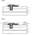
- FIGS. 2 to 6 are schematic cross-sectional views illustrating the semiconductor device in process of manufacture in the manufacturing method for the semiconductor device according to the present embodiment.
- the manufacturing method for the semiconductor device includes: forming a second GaN based semiconductor layer on a first GaN based semiconductor layer by an epitaxial growth process, the second GaN based semiconductor layer having a bandgap larger than a bandgap of the first GaN based semiconductor layer; forming a third p-type GaN based semiconductor layer on the second GaN based semiconductor layer; forming a trench that penetrates through the third p-type GaN based semiconductor layer and reaches the second GaN based semiconductor layer; forming a gate insulating film on the trench and a surface of the third GaN based semiconductor layer; forming a gate electrode on the gate insulating film; forming a source electrode on one side of the gate electrode on the second GaN based semiconductor layer; and forming a drain electrode on the other side of the gate electrode on the second GaN based semiconductor layer.
- the substrate 10, for example, a Si substrate is prepared.
- the buffer layer 12 is grown on the Si substrate, for example, by epitaxial growth.
- the undoped GaN to be the channel layer (first GaN based semiconductor layer) 14 and the undoped Al 0.2 Ga 0.8 N to be the barrier layer (second GaN based semiconductor layer) 16 are formed on the buffer layer 12 by the epitaxial growth.
- the p-type GaN (third GaN based semiconductor layer) 17 to be the resurf layer (third GaN based semiconductor layer) 24 later is formed on the barrier layer 16 by the epitaxial growth ( FIG. 2 ).
- the trench 21 penetrating through the p-type GaN 17 and reaching the barrier layer 16 and the channel layer 14 is formed by, for example, RIE (Reactive Ion Etching) process ( FIG. 4 ).
- the gate electrode 26 made of TiN is formed on the gate insulating film 22 by sputtering method and etching.
- patterning is applied to the gate insulating film 22 and the p-type GaN 17 to form the resurf layer 24 and the resurf layer 54 ( FIG. 5 ).
- the source electrode 18 and the drain electrode 20 having the stacked structure of titanium (Ti) and aluminum (Al) are formed on the barrier layer 16 by a liftoff process ( FIG. 6 ).
- the insulating film 30, source field plate electrode 28, and insulating film 32 are formed, and the semiconductor device 100 illustrated in FIG. 1 is manufactured.
- the p-type GaN 17 may be formed by the epitaxial growth of the undoped GaN and ion implantation of a selective p-type impurity such as magnesium.
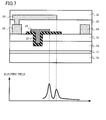
- FIGS. 7 and 8 are explanatory diagrams for the function and effects of the semiconductor device according to the present embodiment.
- FIG. 7 is the diagram illustrating the HEMT without including the resurf layer
- FIG. 8 is the diagram illustrating the HEMT including the resurf layer according to the present embodiment. In the respective cases, distribution of electric field strength when the HEMT is turned off will be schematically illustrated.
- the electric field concentrates on two points, namely, the end portion on the drain electrode 20 side of the gate electrode 26 and the end portion on the drain electrode 20 side of the source field plate electrode 28 at which peaks of the electric field strength appear.
- the concentrated electric field is mainly the lateral electric field.
- the insulating film and the semiconductor may be damaged and the breakdown voltage may be deteriorated at the places where the electric field is concentrated.
- the reason for such electric field concentration at the end portions of the electrodes as shown in FIG. 7 is considered to be discontinuous depletion of a two-dimensional electron gas generated on an interface between the barrier layer 16 and the channel layer 14.
- the peaks of the electric field strength at the end portion on the drain electrode 20 side of the gate electrode 26 and the end portion on the drain electrode 20 side of the source field plate electrode 28 become gentle, and electric field strength becomes smaller compared to the case without including the resurf layer 24.
- the reason is considered that discontinuity of expansion of a depletion layer is reduced by positive charge inside the floating resurf layer 24.
- area density of an acceptor of the resurf layer 24 is lower than the area density of the two-dimensional electron gas generated on the interface between the barrier layer 16 and the channel layer 14 in an area where neither the resurf layer 24 nor the gate electrode 26 is provided.
- the area density of the acceptor of the resurf layer 24 becomes higher than the area density of the above-mentioned two-dimensional electron gas, the density of the two-dimensional electron gas may be decreased and the on-resistance may be increased.
- the area density of the acceptor of the resurf layer 24 is higher than 10% of the area density of the two-dimensional electron gas generated on the interface between the barrier layer 16 and the channel layer 14 in the area where neither the resurf layer 24 nor the gate electrode 26 is provided.
- the area density of the acceptor of the resurf layer 24 becomes lower than the above-mentioned area density, a sufficient effect of electric field alleviation may not be obtained.
- the area density of the two-dimensional electron gas is represented by y ⁇ 4 ⁇ 10 13 [cm -2 ]. Therefore, in this case, the area density of the acceptor of the resurf layer 24 is preferably lower than y ⁇ 4 ⁇ 10 13 [cm -2 ] and higher than y ⁇ 0.4 ⁇ 10 13 [cm -2 ].
- the resurf layer 24 has the film thickness of d [cm] and the acceptor density of N A [cm -3 ], the area density of the acceptor of the resurf layer 24 is represented by d ⁇ N A [cm -2 ]. Therefore, preferably, a relation of a following expression is satisfied: y ⁇ 0.4 ⁇ 10 13 ⁇ d ⁇ N A ⁇ y ⁇ 4 ⁇ 10 13
- an activation rate of the p-type impurity inside a p-type GaN based semiconductor is more or less 10%. Therefore, provided that the atomic percentage of the p-type impurity is N P [cm -2 ], the above (Expression 1) is changed to: y ⁇ 4 ⁇ 10 13 ⁇ d ⁇ N P ⁇ y ⁇ 40 ⁇ 10 13
- the acceptor density of the resurf layer 24 is 1 ⁇ 10 16 cm -3 or more and 1 ⁇ 10 18 cm -3 or less.
- the atomic percentage of the p-type impurity of the resurf layer 24 is preferably 1 ⁇ 10 17 cm -3 or more and 1 ⁇ 10 19 cm -3 or less.
- the film thickness of the resurf layer 24 is preferably 10 nm or more and 100 nm or less.
- the p-type resurf layer 54 is also disposed between the gate electrode 26 and the source electrode 18 on the barrier layer 16.
- the electric field concentration at the end portion on the source electrode 18 side of the gate electrode 26 is alleviated by the resurf layer 54.
- the semiconductor device of the present embodiment the semiconductor device achieving to have high breakdown voltage can be provided by the effect of lateral electric field alleviation by the resurf layers 24 and 54.
- a semiconductor device is same as a first embodiment except for including a second GaN based semiconductor layer between the first GaN based semiconductor layer and a portion of a gate electrode closest to a first GaN based semiconductor layer. Therefore, repetition of describing the matters same as the first embodiment will be omitted.
- FIG. 9 is a schematic cross-sectional view illustrating the semiconductor device according to the present embodiment.
- the semiconductor device according to the present embodiment is an HEMT using a GaN based semiconductor.
- a trench 21 of a semiconductor device (HEMT) 200 is shallower than that of an HEMT 100 of the first embodiment, and a thin barrier layer 16 is located at a bottom portion of the trench 21.
- the thin barrier layer 16 reduces a polarization amount just below a gate electrode 26, and concentration of two-dimensional electron gas is decreased. Therefore, a normally-off type HEMT can be formed.
- the semiconductor device achieving to have high breakdown voltage can be provided same as the first embodiment. Further, since the two-dimensional electron gas exists also in a channel portion just below the gate electrode 26, the semiconductor device having on-resistance lower than the first embodiment can be provided.
- a semiconductor device is same as a first embodiment except for that an interface between a second GaN based semiconductor layer and a gate insulating film is sloped. Therefore, repetition of describing the matters same as the first embodiment will be omitted.
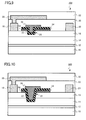
- FIG. 10 is a schematic cross-sectional view illustrating a semiconductor device according to the present embodiment.
- the semiconductor device according to the present embodiment is an HEMT using a GaN based semiconductor.
- a channel layer 14, a barrier layer 16, and an interface between a resurf layer 24 and a gate insulating film 22 are sloped.
- a side surface of a trench 21 is sloped with respect to an interface between the channel layer 14 and the barrier layer 16, instead of being vertical thereto.
- an effect of electric field alleviation is more increased by the sloped side surface of the trench 21, and the semiconductor device achieving to have higher breakdown voltage can be provided.
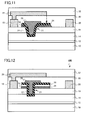
- FIG. 11 is a schematic cross-sectional view illustrating a modified example of the semiconductor device according to the present embodiment.
- the side surface of the trench 21 is gently sloped toward an upper portion of the trench 21 from the standpoint of electric field alleviation.
- a side wall of the end portion on the drain electrode 20 side of the resurf layer 24 is also sloped as illustrated in FIG. 11 from the standpoint of electric field alleviation at the end portion of the resurf layer 24.
- a semiconductor device is same as a first embodiment except for further including a protection film made of a material different from a gate insulating film and disposed between the gate insulating film and a third GaN based semiconductor layer. Therefore, repetition of describing the matters same as the first embodiment will be omitted.
- FIG. 12 is a schematic cross-sectional view illustrating the semiconductor device according to the present embodiment.
- the semiconductor device according to the present embodiment is an HEMT using a GaN based semiconductor.
- a semiconductor device (HEMT) 400 includes a protection film 38 made of the material different from a gate insulating film 22 and disposed between the gate insulating film 22 and a resurf layer 24.
- the protection film 38 is a silicon nitride film or a silicon oxynitride film.
- an interface level in a space with the resurf layer 24 is lowered by using the silicon nitride film or silicon oxynitride film as the protection film 38. Therefore, for example, current collapse hardly occurs, and reliability of the HEMT is improved. Further, since the protection film 38 is interposed between the gate electrode 26 and the resurf layer 24, an electric field applied to the gate insulating film 22 is alleviated, thereby improving reliability.
- the semiconductor device achieving to have high breakdown voltage can be provided same as the first embodiment. Further, the semiconductor device having excellent reliability can be provided.
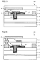
- FIG. 13 is a schematic cross-sectional view illustrating a modified example of the semiconductor device according to the present embodiment. From the standpoint of improvement of reliability on the gate insulating film 22, a configuration in which the protection film 38 is disposed between the gate insulating film 22 and the resurf layer 24 at a side surface portion of a trench 21 may also be possible as illustrated in FIG. 13 .
- a semiconductor device is same as a first p-type embodiment except for further including a fifth GaN based semiconductor layer disposed between a third GaN based semiconductor layer and a drain electrode on a second GaN based semiconductor layer on an opposite side of a first GaN based semiconductor layer, and separated from the third GaN based semiconductor layer. Therefore, repetition of describing the matters same as the first embodiment will be omitted.
- FIG. 14 is a schematic cross-sectional view illustrating the semiconductor device according to the present embodiment.
- the semiconductor device according to the present embodiment is an HEMT using a GaN based semiconductor.
- a semiconductor device (HEMT) 500 includes a plurality of resurf layers, more specifically, a resurf layer (third GaN based semiconductor layer) 24, a resurf layer (fifth GaN based semiconductor layer) 34, and a resurf layer (fifth GaN based semiconductor layer) 36, between a gate electrode 26 and a drain electrode 20.
- the resurf layers (fifth GaN based semiconductor layers) 34, 36 are disposed between the resurf layer 24 and the drain electrode 20 on a barrier layer 16.
- the resurf layers 34, 36 are separated from the resurf layer 24.
- the plurality of the resurf layers is disposed between the gate electrode 26 and the drain electrode 20 on the barrier layer 16, thereby further alleviating a lateral electric field and achieving to provide the semiconductor device have high breakdown voltage.
- a semiconductor device is same as a first embodiment except for including a sixth i-type GaN based semiconductor layer between a second GaN based semiconductor layer and a third GaN based semiconductor layer. Therefore, repetition of describing the matters same as the first embodiment will be omitted.
- FIG. 15 is a schematic cross-sectional view illustrating the semiconductor device according to the present embodiment.
- the semiconductor device according to the present embodiment is an HEMT using a GaN based semiconductor.
- a semiconductor device (HEMT) 600 includes an i (intrinsic) type GaN layer (sixth GaN based semiconductor layer) 40 between a barrier layer 16 and a resurf layer 24.
- a lateral electric field is alleviated by the resurf layer 24 and the semiconductor device achieving to have high breakdown voltage can be provided.
- a semiconductor device is same as a first embodiment except for further including a second field plate electrode, interposing an insulating film in a space with a first field plate electrode and interposing an insulating film in a space with a third GaN based semiconductor layer, and the third GaN based semiconductor layer is located between a second GaN based semiconductor layer and an end portion on a drain electrode side of the second field plate electrode. Therefore, repetition of describing the matters same as the first embodiment will be omitted.
- FIG. 16 is a schematic cross-sectional view of the semiconductor device according to the present embodiment.
- the semiconductor device according to the present embodiment is an HEMT using a GaN based semiconductor.
- a semiconductor device (HEMT) 700 includes a gate field plate electrode (second field plate electrode) 42, interposing an insulating film 32 in the space with a source field plate electrode (first field plate electrode) 28 and also interposing an insulating film 30 in a space with a resurf layer 24.
- the resurf layer 24 is located between a barrier layer 16 (second GaN based semiconductor layer) and an end portion on a drain electrode 20 side of the gate field plate electrode 42.
- concentration of a lateral electric field at the end portion on the drain electrode 20 side of the gate field plate electrode 42 is alleviated by the resurf layer 24.
- the semiconductor device of the present embodiment the semiconductor device achieving to have high breakdown voltage can be provided by including the gate field plate electrode 42, in addition to effects of the first embodiment.
- a semiconductor device is same as a first embodiment except for further including: a seventh GaN based semiconductor layer between a buffer layer and a channel layer; and an eighth GaN based semiconductor layer disposed on the seventh GaN based semiconductor layer and having a bandgap larger than a bandgap of the seventh GaN based semiconductor layer. Therefore, repetition of describing the matters same as the first embodiment will be omitted.
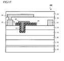
- FIG. 17 is a schematic cross-sectional view of the semiconductor device according to the present embodiment.
- the semiconductor device according to the present embodiment is an HEMT using a GaN based semiconductor.
- a semiconductor device (HEMT) 800 includes a second channel layer 64 and a second barrier layer 66 on a buffer layer 12.
- the second channel layer 64 is, for example, undoped Al X Ga 1-X N (1 ⁇ X ⁇ 0).
- the second channel layer 64 is undoped GaN, for example.
- the second channel layer 64 has film thickness of 0.5 ⁇ m or more and 3 ⁇ m or less.
- the second barrier layer 66 is disposed on the second channel layer 64.
- the second barrier layer 66 has the bandgap larger than the bandgap of the second channel layer 64.
- the second barrier layer 66 is, for example, undoped Al Y Ga 1-Y N (0 ⁇ Y ⁇ 1, X ⁇ Y). More specifically, the barrier layer is undoped Al 0.2 Ga 0.8 N, for example.
- the second barrier layer 66 has the film thickness of, for example, 3 nm or more and 50 nm or less.
- a heterojunction interface is provided between the second channel layer 64 and the second barrier layer 66.
- 2DEG two-dimensional electron gas
- the two-dimensional electron gas (2DEG) is formed in the two layers. Therefore, the HEMT having lowered on-resistance can be achieved.
- a lateral electric field is alleviated by the resurf layer 24 and the semiconductor device achieving to have high breakdown voltage can be provided. Further, the semiconductor device having the more lowered on-resistance can be provided.
- a semiconductor device is same as a first embodiment except for not including a first field plate electrode. Therefore, repetition of describing the matters same as the first embodiment will be omitted.
- FIG. 18 is a schematic cross-sectional view illustrating the semiconductor device according to the present embodiment.
- the semiconductor device according to the present embodiment is an HEMT using a GaN based semiconductor.
- a semiconductor device (HEMT) 900 does not include the source field plate electrode, different from an HEMT 100 of the first embodiment.
- concentration of an electric field at an end portion on a drain electrode 20 side of a gate electrode 26 is alleviated by a resurf layer 24. Therefore, according to the present embodiment, the semiconductor device capable of reducing parasitic capacitance in a space with the field plate electrode and also achieving to have high breakdown voltage can be provided by an effect of lateral electric field alleviation by the resurf layer 24.
- GaN and AlGaN as the material of the GaN based semiconductor layer have been described, but InGaN, InAlN, and InAlGaN including indium (In), for example, may also be applicable.
- AIN may be applied as the material of the GaN based semiconductor layer.
- n-type AlGaN may also be applicable.
Landscapes
- Junction Field-Effect Transistors (AREA)
- Insulated Gate Type Field-Effect Transistor (AREA)
- Thin Film Transistor (AREA)
- Electrodes Of Semiconductors (AREA)
Applications Claiming Priority (1)
| Application Number | Priority Date | Filing Date | Title |
|---|---|---|---|
| JP2014057282A JP6270572B2 (ja) | 2014-03-19 | 2014-03-19 | 半導体装置及びその製造方法 |
Publications (2)
| Publication Number | Publication Date |
|---|---|
| EP2922096A2 true EP2922096A2 (fr) | 2015-09-23 |
| EP2922096A3 EP2922096A3 (fr) | 2016-03-02 |
Family
ID=52577786
Family Applications (1)
| Application Number | Title | Priority Date | Filing Date |
|---|---|---|---|
| EP15157014.0A Withdrawn EP2922096A3 (fr) | 2014-03-19 | 2015-02-27 | Dispositif à semi-conducteurs et procédé de fabrication de celui-ci |
Country Status (5)
| Country | Link |
|---|---|
| US (1) | US9461122B2 (fr) |
| EP (1) | EP2922096A3 (fr) |
| JP (1) | JP6270572B2 (fr) |
| CN (1) | CN104934476B (fr) |
| TW (1) | TWI550858B (fr) |
Families Citing this family (57)
| Publication number | Priority date | Publication date | Assignee | Title |
|---|---|---|---|---|
| JP6171435B2 (ja) | 2013-03-18 | 2017-08-02 | 富士通株式会社 | 半導体装置及びその製造方法、電源装置、高周波増幅器 |
| JP6220161B2 (ja) | 2013-06-03 | 2017-10-25 | ルネサスエレクトロニクス株式会社 | 半導体装置の製造方法 |
| US9761438B1 (en) * | 2014-05-08 | 2017-09-12 | Hrl Laboratories, Llc | Method for manufacturing a semiconductor structure having a passivated III-nitride layer |
| JP6401053B2 (ja) * | 2014-12-26 | 2018-10-03 | ルネサスエレクトロニクス株式会社 | 半導体装置および半導体装置の製造方法 |
| JP6332021B2 (ja) * | 2014-12-26 | 2018-05-30 | 株式会社デンソー | 半導体装置 |
| JP6462393B2 (ja) * | 2015-02-10 | 2019-01-30 | ルネサスエレクトロニクス株式会社 | 半導体装置の製造方法および半導体装置 |
| CN106601792A (zh) * | 2015-10-15 | 2017-04-26 | 北京大学 | 一种氮化镓高电子迁移率晶体管及其制备方法 |
| TWI670851B (zh) * | 2015-10-28 | 2019-09-01 | 晶元光電股份有限公司 | 半導體功率元件 |
| ITUB20155536A1 (it) * | 2015-11-12 | 2017-05-12 | St Microelectronics Srl | Transistore hemt di tipo normalmente spento includente una trincea contenente una regione di gate e formante almeno un gradino, e relativo procedimento di fabbricazione |
| ITUB20155862A1 (it) * | 2015-11-24 | 2017-05-24 | St Microelectronics Srl | Transistore di tipo normalmente spento con ridotta resistenza in stato acceso e relativo metodo di fabbricazione |
| CN107230716A (zh) * | 2016-03-25 | 2017-10-03 | 北京大学 | 氮化镓晶体管的制备方法 |
| US20180076310A1 (en) * | 2016-08-23 | 2018-03-15 | David Sheridan | Asymmetrical blocking bidirectional gallium nitride switch |
| JP7154015B2 (ja) * | 2017-03-03 | 2022-10-17 | パワー・インテグレーションズ・インコーポレーテッド | 電荷分配構造物を含むスイッチングデバイス |
| CN107316894B (zh) * | 2017-06-23 | 2020-06-05 | 深圳市晶相技术有限公司 | 氮化镓半导体器件及其制备方法 |
| CN107316895A (zh) * | 2017-06-23 | 2017-11-03 | 深圳市晶相技术有限公司 | 氮化镓半导体器件及其制备方法 |
| CN107393962A (zh) * | 2017-06-23 | 2017-11-24 | 深圳市晶相技术有限公司 | 氮化镓半导体器件及其制备方法 |
| CN107437560B (zh) * | 2017-06-23 | 2020-06-05 | 深圳市晶相技术有限公司 | 氮化镓半导体器件及其制备方法 |
| CN107331696A (zh) * | 2017-06-23 | 2017-11-07 | 深圳市晶相技术有限公司 | 氮化镓半导体器件及其制备方法 |
| CN107331697A (zh) * | 2017-06-23 | 2017-11-07 | 深圳市晶相技术有限公司 | 氮化镓半导体器件及其制备方法 |
| CN107316892B (zh) * | 2017-06-23 | 2020-08-21 | 深圳市晶相技术有限公司 | 氮化镓半导体器件及其制备方法 |
| CN107275384B (zh) * | 2017-06-23 | 2020-09-25 | 深圳市晶相技术有限公司 | 氮化镓半导体器件及其制备方法 |
| CN107275386A (zh) * | 2017-06-23 | 2017-10-20 | 深圳市晶相技术有限公司 | 氮化镓半导体器件及其制备方法 |
| CN107393963B (zh) * | 2017-06-23 | 2020-09-25 | 深圳市晶相技术有限公司 | 氮化镓半导体器件及其制备方法 |
| CN107275385B (zh) * | 2017-06-23 | 2020-08-21 | 深圳市晶相技术有限公司 | 氮化镓半导体器件及其制备方法 |
| CN107248525B (zh) * | 2017-06-23 | 2020-08-21 | 深圳市晶相技术有限公司 | 氮化镓半导体器件及其制备方法 |
| CN107248524B (zh) * | 2017-06-23 | 2020-08-21 | 深圳市晶相技术有限公司 | 氮化镓半导体器件及其制备方法 |
| CN107316890A (zh) * | 2017-06-23 | 2017-11-03 | 深圳市晶相技术有限公司 | 氮化镓半导体器件及其制备方法 |
| CN107316891A (zh) * | 2017-06-23 | 2017-11-03 | 深圳市晶相技术有限公司 | 氮化镓半导体器件及其制备方法 |
| CN107316893A (zh) * | 2017-06-23 | 2017-11-03 | 深圳市晶相技术有限公司 | 氮化镓半导体器件及其制备方法 |
| CN107293577B (zh) * | 2017-06-23 | 2020-08-21 | 深圳市晶相技术有限公司 | 氮化镓半导体器件及其制备方法 |
| CN107248526B (zh) * | 2017-06-23 | 2020-10-16 | 深圳市晶相技术有限公司 | 氮化镓半导体器件及其制备方法 |
| TWI635611B (zh) * | 2017-09-25 | 2018-09-11 | Nuvoton Technology Corporation | 高壓半導體元件 |
| CN107644915B (zh) * | 2017-09-28 | 2019-09-13 | 英诺赛科(苏州)半导体有限公司 | 具有局部p型帽层的晶体管器件 |
| JP7021034B2 (ja) | 2018-09-18 | 2022-02-16 | 株式会社東芝 | 半導体装置 |
| US11316038B2 (en) | 2018-11-20 | 2022-04-26 | Stmicroelectronics S.R.L. | HEMT transistor with adjusted gate-source distance, and manufacturing method thereof |
| US10818787B1 (en) * | 2019-04-18 | 2020-10-27 | Semiconductor Components Industries, Llc | Electronic device including a high electron mobility transistor including a gate electrode and a dielectric film |
| JP7448314B2 (ja) * | 2019-04-19 | 2024-03-12 | 株式会社東芝 | 半導体装置 |
| JP7368107B2 (ja) | 2019-05-22 | 2023-10-24 | 株式会社東芝 | 半導体装置 |
| US11038048B2 (en) * | 2019-10-01 | 2021-06-15 | Taiwan Semiconductor Manufacturing Company, Ltd. | Gallium nitride-on-silicon devices |
| US10930745B1 (en) * | 2019-11-27 | 2021-02-23 | Vanguard International Semiconductor Corporation | Semiconductor structure |
| US11855198B2 (en) * | 2020-04-09 | 2023-12-26 | Qualcomm Incorporated | Multi-gate high electron mobility transistors (HEMTs) employing tuned recess depth gates for improved device linearity |
| JP7450446B2 (ja) | 2020-04-13 | 2024-03-15 | 株式会社アドバンテスト | 半導体装置、半導体装置の製造方法、および試験装置 |
| EP4135010B1 (fr) | 2020-05-13 | 2026-01-21 | Nuvoton Technology Corporation Japan | Dispositif à semi-conducteur pour amplification de puissance |
| FR3110770B1 (fr) | 2020-05-19 | 2022-04-29 | Commissariat Energie Atomique | Composant électronique à hétérojonction comprenant une plaque de champ et une région flottante dopée p |
| JP7470008B2 (ja) * | 2020-10-19 | 2024-04-17 | 株式会社東芝 | 半導体装置 |
| JP7437346B2 (ja) | 2021-04-15 | 2024-02-22 | 株式会社東芝 | 半導体装置及びその製造方法 |
| CN113257896B (zh) * | 2021-05-11 | 2024-06-18 | 华南师范大学 | 多场板射频hemt器件及其制备方法 |
| CN115458580B (zh) * | 2021-06-08 | 2025-12-09 | 株式会社东芝 | 半导体装置 |
| CN113517335B (zh) * | 2021-06-13 | 2023-07-25 | 华南师范大学 | 一种可调节的复合凹槽栅e-hemt器件及制备方法 |
| CN115621310B (zh) | 2021-07-16 | 2026-01-02 | 联华电子股份有限公司 | 半导体装置以及其制作方法 |
| JP7705811B2 (ja) * | 2021-08-27 | 2025-07-10 | 株式会社東芝 | 半導体装置 |
| CN117836951A (zh) * | 2021-09-07 | 2024-04-05 | 株式会社日本显示器 | 晶体管 |
| CN115810663B (zh) | 2021-09-14 | 2026-04-03 | 联华电子股份有限公司 | 高电子迁移率晶体管及其制作方法 |
| CN113871480A (zh) * | 2021-09-29 | 2021-12-31 | 西安电子科技大学 | 常关型沟道调制器件及其制作方法 |
| CN116344604B (zh) * | 2021-12-23 | 2026-04-03 | 联华电子股份有限公司 | 绝缘栅双极型晶体管 |
| CN117423725A (zh) * | 2023-12-01 | 2024-01-19 | 江苏希尔半导体有限公司 | 一种高压横向GaN高电子迁移率晶体管 |
| WO2026062853A1 (fr) * | 2024-09-19 | 2026-03-26 | 株式会社 東芝 | Dispositif à semi-conducteur |
Family Cites Families (19)
| Publication number | Priority date | Publication date | Assignee | Title |
|---|---|---|---|---|
| KR100573720B1 (ko) | 2003-01-29 | 2006-04-26 | 가부시끼가이샤 도시바 | 전력 반도체소자 |
| JP4041075B2 (ja) * | 2004-02-27 | 2008-01-30 | 株式会社東芝 | 半導体装置 |
| US7126166B2 (en) * | 2004-03-11 | 2006-10-24 | Semiconductor Components Industries, L.L.C. | High voltage lateral FET structure with improved on resistance performance |
| JP4944402B2 (ja) | 2005-07-13 | 2012-05-30 | ルネサスエレクトロニクス株式会社 | 半導体装置 |
| JP4751150B2 (ja) | 2005-08-31 | 2011-08-17 | 株式会社東芝 | 窒化物系半導体装置 |
| JP4761319B2 (ja) * | 2008-02-19 | 2011-08-31 | シャープ株式会社 | 窒化物半導体装置とそれを含む電力変換装置 |
| JP5144326B2 (ja) | 2008-03-21 | 2013-02-13 | 古河電気工業株式会社 | 電界効果トランジスタ |
| JP2009246205A (ja) | 2008-03-31 | 2009-10-22 | Furukawa Electric Co Ltd:The | 半導体装置および半導体装置の製造方法 |
| JP5323527B2 (ja) * | 2009-02-18 | 2013-10-23 | 古河電気工業株式会社 | GaN系電界効果トランジスタの製造方法 |
| JP5530682B2 (ja) * | 2009-09-03 | 2014-06-25 | パナソニック株式会社 | 窒化物半導体装置 |
| JP2012109348A (ja) * | 2010-11-16 | 2012-06-07 | Sumitomo Electric Ind Ltd | 炭化珪素半導体装置 |
| KR20120120825A (ko) | 2011-04-25 | 2012-11-02 | 삼성전기주식회사 | 질화물 반도체 소자 및 그 제조방법 |
| TWI544628B (zh) * | 2011-05-16 | 2016-08-01 | 瑞薩電子股份有限公司 | Field effect transistor and semiconductor device |
| JP5979836B2 (ja) | 2011-09-09 | 2016-08-31 | ルネサスエレクトロニクス株式会社 | 半導体装置および半導体装置の製造方法 |
| JP2013093482A (ja) | 2011-10-27 | 2013-05-16 | Renesas Electronics Corp | 半導体装置および半導体装置の製造方法 |
| US8921893B2 (en) * | 2011-12-01 | 2014-12-30 | Taiwan Semiconductor Manufacturing Company, Ltd. | Circuit structure having islands between source and drain |
| JP2013149851A (ja) | 2012-01-20 | 2013-08-01 | Sharp Corp | 窒化物半導体装置 |
| JP2013191637A (ja) * | 2012-03-12 | 2013-09-26 | Advanced Power Device Research Association | 窒化物系化合物半導体素子 |
| JP6013948B2 (ja) * | 2013-03-13 | 2016-10-25 | ルネサスエレクトロニクス株式会社 | 半導体装置 |
-
2014
- 2014-03-19 JP JP2014057282A patent/JP6270572B2/ja active Active
-
2015
- 2015-02-26 TW TW104106324A patent/TWI550858B/zh active
- 2015-02-27 EP EP15157014.0A patent/EP2922096A3/fr not_active Withdrawn
- 2015-03-09 US US14/642,146 patent/US9461122B2/en active Active
- 2015-03-12 CN CN201510108951.5A patent/CN104934476B/zh active Active
Non-Patent Citations (1)
| Title |
|---|
| None |
Also Published As
| Publication number | Publication date |
|---|---|
| TW201539753A (zh) | 2015-10-16 |
| JP6270572B2 (ja) | 2018-01-31 |
| JP2015179786A (ja) | 2015-10-08 |
| CN104934476B (zh) | 2018-03-16 |
| US9461122B2 (en) | 2016-10-04 |
| EP2922096A3 (fr) | 2016-03-02 |
| TWI550858B (zh) | 2016-09-21 |
| CN104934476A (zh) | 2015-09-23 |
| US20150270355A1 (en) | 2015-09-24 |
Similar Documents
| Publication | Publication Date | Title |
|---|---|---|
| US9461122B2 (en) | Semiconductor device and manufacturing method for the same | |
| US10714566B2 (en) | Semiconductor device | |
| US10043896B2 (en) | III-Nitride transistor including a III-N depleting layer | |
| US11114554B2 (en) | High-electron-mobility transistor having a buried field plate | |
| US9349829B2 (en) | Method of manufacturing a multi-channel HEMT | |
| US9406792B2 (en) | Semiconductor device having GaN-based layer | |
| US8928003B2 (en) | Nitride semiconductor device | |
| US9171730B2 (en) | Electrodes for semiconductor devices and methods of forming the same | |
| JP5691267B2 (ja) | 半導体装置 | |
| US20250040175A1 (en) | A vertical hemt, an electrical circuit, and a method for producing a vertical hemt | |
| US10211305B2 (en) | Normally-off hetrojunction transistor with high threshold voltage | |
| CN104916682A (zh) | 半导体装置 | |
| CN104916679A (zh) | 半导体装置 | |
| JP2025125348A (ja) | 窒化物半導体デバイス |
Legal Events
| Date | Code | Title | Description |
|---|---|---|---|
| PUAI | Public reference made under article 153(3) epc to a published international application that has entered the european phase |
Free format text: ORIGINAL CODE: 0009012 |
|
| 17P | Request for examination filed |
Effective date: 20150227 |
|
| AK | Designated contracting states |
Kind code of ref document: A2 Designated state(s): AL AT BE BG CH CY CZ DE DK EE ES FI FR GB GR HR HU IE IS IT LI LT LU LV MC MK MT NL NO PL PT RO RS SE SI SK SM TR |
|
| AX | Request for extension of the european patent |
Extension state: BA ME |
|
| PUAL | Search report despatched |
Free format text: ORIGINAL CODE: 0009013 |
|
| AK | Designated contracting states |
Kind code of ref document: A3 Designated state(s): AL AT BE BG CH CY CZ DE DK EE ES FI FR GB GR HR HU IE IS IT LI LT LU LV MC MK MT NL NO PL PT RO RS SE SI SK SM TR |
|
| AX | Request for extension of the european patent |
Extension state: BA ME |
|
| RIC1 | Information provided on ipc code assigned before grant |
Ipc: H01L 29/40 20060101ALN20160125BHEP Ipc: H01L 29/20 20060101ALN20160125BHEP Ipc: H01L 29/423 20060101ALN20160125BHEP Ipc: H01L 29/06 20060101ALI20160125BHEP Ipc: H01L 29/778 20060101AFI20160125BHEP Ipc: H01L 21/336 20060101ALI20160125BHEP |
|
| STAA | Information on the status of an ep patent application or granted ep patent |
Free format text: STATUS: EXAMINATION IS IN PROGRESS |
|
| 17Q | First examination report despatched |
Effective date: 20170622 |
|
| GRAC | Information related to communication of intention to grant a patent modified |
Free format text: ORIGINAL CODE: EPIDOSCIGR1 |
|
| STAA | Information on the status of an ep patent application or granted ep patent |
Free format text: STATUS: GRANT OF PATENT IS INTENDED |
|
| GRAP | Despatch of communication of intention to grant a patent |
Free format text: ORIGINAL CODE: EPIDOSNIGR1 |
|
| STAA | Information on the status of an ep patent application or granted ep patent |
Free format text: STATUS: EXAMINATION IS IN PROGRESS |
|
| GRAJ | Information related to disapproval of communication of intention to grant by the applicant or resumption of examination proceedings by the epo deleted |
Free format text: ORIGINAL CODE: EPIDOSDIGR1 |
|
| GRAP | Despatch of communication of intention to grant a patent |
Free format text: ORIGINAL CODE: EPIDOSNIGR1 |
|
| RIC1 | Information provided on ipc code assigned before grant |
Ipc: H01L 29/40 20060101ALN20190701BHEP Ipc: H01L 29/20 20060101ALN20190701BHEP Ipc: H01L 29/423 20060101ALN20190701BHEP Ipc: H01L 29/778 20060101AFI20190701BHEP Ipc: H01L 29/06 20060101ALI20190701BHEP Ipc: H01L 21/336 20060101ALI20190701BHEP |
|
| GRAP | Despatch of communication of intention to grant a patent |
Free format text: ORIGINAL CODE: EPIDOSNIGR1 |
|
| STAA | Information on the status of an ep patent application or granted ep patent |
Free format text: STATUS: GRANT OF PATENT IS INTENDED |
|
| INTG | Intention to grant announced |
Effective date: 20190802 |
|
| INTC | Intention to grant announced (deleted) | ||
| RIC1 | Information provided on ipc code assigned before grant |
Ipc: H01L 21/336 20060101ALI20190801BHEP Ipc: H01L 29/20 20060101ALN20190801BHEP Ipc: H01L 29/06 20060101ALI20190801BHEP Ipc: H01L 29/778 20060101AFI20190801BHEP Ipc: H01L 29/40 20060101ALN20190801BHEP Ipc: H01L 29/423 20060101ALN20190801BHEP |
|
| INTG | Intention to grant announced |
Effective date: 20190813 |
|
| STAA | Information on the status of an ep patent application or granted ep patent |
Free format text: STATUS: THE APPLICATION IS DEEMED TO BE WITHDRAWN |
|
| 18D | Application deemed to be withdrawn |
Effective date: 20200103 |