EP2922980B1 - Chargement de substrat dans un réacteur ald - Google Patents
Chargement de substrat dans un réacteur ald Download PDFInfo
- Publication number
- EP2922980B1 EP2922980B1 EP12888893.0A EP12888893A EP2922980B1 EP 2922980 B1 EP2922980 B1 EP 2922980B1 EP 12888893 A EP12888893 A EP 12888893A EP 2922980 B1 EP2922980 B1 EP 2922980B1
- Authority
- EP
- European Patent Office
- Prior art keywords
- loading
- chamber
- substrate holder
- substrates
- substrate
- Prior art date
- Legal status (The legal status is an assumption and is not a legal conclusion. Google has not performed a legal analysis and makes no representation as to the accuracy of the status listed.)
- Active
Links
Images



Classifications
-
- C—CHEMISTRY; METALLURGY
- C23—COATING METALLIC MATERIAL; COATING MATERIAL WITH METALLIC MATERIAL; CHEMICAL SURFACE TREATMENT; DIFFUSION TREATMENT OF METALLIC MATERIAL; COATING BY VACUUM EVAPORATION, BY SPUTTERING, BY ION IMPLANTATION OR BY CHEMICAL VAPOUR DEPOSITION, IN GENERAL; INHIBITING CORROSION OF METALLIC MATERIAL OR INCRUSTATION IN GENERAL
- C23C—COATING METALLIC MATERIAL; COATING MATERIAL WITH METALLIC MATERIAL; SURFACE TREATMENT OF METALLIC MATERIAL BY DIFFUSION INTO THE SURFACE, BY CHEMICAL CONVERSION OR SUBSTITUTION; COATING BY VACUUM EVAPORATION, BY SPUTTERING, BY ION IMPLANTATION OR BY CHEMICAL VAPOUR DEPOSITION, IN GENERAL
- C23C16/00—Chemical coating by decomposition of gaseous compounds, without leaving reaction products of surface material in the coating, i.e. chemical vapour deposition [CVD] processes
- C23C16/44—Chemical coating by decomposition of gaseous compounds, without leaving reaction products of surface material in the coating, i.e. chemical vapour deposition [CVD] processes characterised by the method of coating
- C23C16/458—Chemical coating by decomposition of gaseous compounds, without leaving reaction products of surface material in the coating, i.e. chemical vapour deposition [CVD] processes characterised by the method of coating characterised by the method used for supporting substrates in the reaction chamber
- C23C16/4582—Rigid and flat substrates, e.g. plates or discs
- C23C16/4583—Rigid and flat substrates, e.g. plates or discs the substrate being supported substantially horizontally
-
- C—CHEMISTRY; METALLURGY
- C23—COATING METALLIC MATERIAL; COATING MATERIAL WITH METALLIC MATERIAL; CHEMICAL SURFACE TREATMENT; DIFFUSION TREATMENT OF METALLIC MATERIAL; COATING BY VACUUM EVAPORATION, BY SPUTTERING, BY ION IMPLANTATION OR BY CHEMICAL VAPOUR DEPOSITION, IN GENERAL; INHIBITING CORROSION OF METALLIC MATERIAL OR INCRUSTATION IN GENERAL
- C23C—COATING METALLIC MATERIAL; COATING MATERIAL WITH METALLIC MATERIAL; SURFACE TREATMENT OF METALLIC MATERIAL BY DIFFUSION INTO THE SURFACE, BY CHEMICAL CONVERSION OR SUBSTITUTION; COATING BY VACUUM EVAPORATION, BY SPUTTERING, BY ION IMPLANTATION OR BY CHEMICAL VAPOUR DEPOSITION, IN GENERAL
- C23C16/00—Chemical coating by decomposition of gaseous compounds, without leaving reaction products of surface material in the coating, i.e. chemical vapour deposition [CVD] processes
- C23C16/44—Chemical coating by decomposition of gaseous compounds, without leaving reaction products of surface material in the coating, i.e. chemical vapour deposition [CVD] processes characterised by the method of coating
- C23C16/455—Chemical coating by decomposition of gaseous compounds, without leaving reaction products of surface material in the coating, i.e. chemical vapour deposition [CVD] processes characterised by the method of coating characterised by the method used for introducing gases into reaction chamber or for modifying gas flows in reaction chamber
- C23C16/45523—Pulsed gas flow or change of composition over time
- C23C16/45525—Atomic layer deposition [ALD]
- C23C16/45544—Atomic layer deposition [ALD] characterized by the apparatus
- C23C16/45546—Atomic layer deposition [ALD] characterized by the apparatus specially adapted for a substrate stack in the ALD reactor
-
- C—CHEMISTRY; METALLURGY
- C23—COATING METALLIC MATERIAL; COATING MATERIAL WITH METALLIC MATERIAL; CHEMICAL SURFACE TREATMENT; DIFFUSION TREATMENT OF METALLIC MATERIAL; COATING BY VACUUM EVAPORATION, BY SPUTTERING, BY ION IMPLANTATION OR BY CHEMICAL VAPOUR DEPOSITION, IN GENERAL; INHIBITING CORROSION OF METALLIC MATERIAL OR INCRUSTATION IN GENERAL
- C23C—COATING METALLIC MATERIAL; COATING MATERIAL WITH METALLIC MATERIAL; SURFACE TREATMENT OF METALLIC MATERIAL BY DIFFUSION INTO THE SURFACE, BY CHEMICAL CONVERSION OR SUBSTITUTION; COATING BY VACUUM EVAPORATION, BY SPUTTERING, BY ION IMPLANTATION OR BY CHEMICAL VAPOUR DEPOSITION, IN GENERAL
- C23C16/00—Chemical coating by decomposition of gaseous compounds, without leaving reaction products of surface material in the coating, i.e. chemical vapour deposition [CVD] processes
- C23C16/44—Chemical coating by decomposition of gaseous compounds, without leaving reaction products of surface material in the coating, i.e. chemical vapour deposition [CVD] processes characterised by the method of coating
- C23C16/455—Chemical coating by decomposition of gaseous compounds, without leaving reaction products of surface material in the coating, i.e. chemical vapour deposition [CVD] processes characterised by the method of coating characterised by the method used for introducing gases into reaction chamber or for modifying gas flows in reaction chamber
-
- C—CHEMISTRY; METALLURGY
- C23—COATING METALLIC MATERIAL; COATING MATERIAL WITH METALLIC MATERIAL; CHEMICAL SURFACE TREATMENT; DIFFUSION TREATMENT OF METALLIC MATERIAL; COATING BY VACUUM EVAPORATION, BY SPUTTERING, BY ION IMPLANTATION OR BY CHEMICAL VAPOUR DEPOSITION, IN GENERAL; INHIBITING CORROSION OF METALLIC MATERIAL OR INCRUSTATION IN GENERAL
- C23C—COATING METALLIC MATERIAL; COATING MATERIAL WITH METALLIC MATERIAL; SURFACE TREATMENT OF METALLIC MATERIAL BY DIFFUSION INTO THE SURFACE, BY CHEMICAL CONVERSION OR SUBSTITUTION; COATING BY VACUUM EVAPORATION, BY SPUTTERING, BY ION IMPLANTATION OR BY CHEMICAL VAPOUR DEPOSITION, IN GENERAL
- C23C16/00—Chemical coating by decomposition of gaseous compounds, without leaving reaction products of surface material in the coating, i.e. chemical vapour deposition [CVD] processes
- C23C16/44—Chemical coating by decomposition of gaseous compounds, without leaving reaction products of surface material in the coating, i.e. chemical vapour deposition [CVD] processes characterised by the method of coating
- C23C16/455—Chemical coating by decomposition of gaseous compounds, without leaving reaction products of surface material in the coating, i.e. chemical vapour deposition [CVD] processes characterised by the method of coating characterised by the method used for introducing gases into reaction chamber or for modifying gas flows in reaction chamber
- C23C16/45523—Pulsed gas flow or change of composition over time
- C23C16/45525—Atomic layer deposition [ALD]
-
- C—CHEMISTRY; METALLURGY
- C23—COATING METALLIC MATERIAL; COATING MATERIAL WITH METALLIC MATERIAL; CHEMICAL SURFACE TREATMENT; DIFFUSION TREATMENT OF METALLIC MATERIAL; COATING BY VACUUM EVAPORATION, BY SPUTTERING, BY ION IMPLANTATION OR BY CHEMICAL VAPOUR DEPOSITION, IN GENERAL; INHIBITING CORROSION OF METALLIC MATERIAL OR INCRUSTATION IN GENERAL
- C23C—COATING METALLIC MATERIAL; COATING MATERIAL WITH METALLIC MATERIAL; SURFACE TREATMENT OF METALLIC MATERIAL BY DIFFUSION INTO THE SURFACE, BY CHEMICAL CONVERSION OR SUBSTITUTION; COATING BY VACUUM EVAPORATION, BY SPUTTERING, BY ION IMPLANTATION OR BY CHEMICAL VAPOUR DEPOSITION, IN GENERAL
- C23C16/00—Chemical coating by decomposition of gaseous compounds, without leaving reaction products of surface material in the coating, i.e. chemical vapour deposition [CVD] processes
- C23C16/44—Chemical coating by decomposition of gaseous compounds, without leaving reaction products of surface material in the coating, i.e. chemical vapour deposition [CVD] processes characterised by the method of coating
- C23C16/458—Chemical coating by decomposition of gaseous compounds, without leaving reaction products of surface material in the coating, i.e. chemical vapour deposition [CVD] processes characterised by the method of coating characterised by the method used for supporting substrates in the reaction chamber
-
- C—CHEMISTRY; METALLURGY
- C23—COATING METALLIC MATERIAL; COATING MATERIAL WITH METALLIC MATERIAL; CHEMICAL SURFACE TREATMENT; DIFFUSION TREATMENT OF METALLIC MATERIAL; COATING BY VACUUM EVAPORATION, BY SPUTTERING, BY ION IMPLANTATION OR BY CHEMICAL VAPOUR DEPOSITION, IN GENERAL; INHIBITING CORROSION OF METALLIC MATERIAL OR INCRUSTATION IN GENERAL
- C23C—COATING METALLIC MATERIAL; COATING MATERIAL WITH METALLIC MATERIAL; SURFACE TREATMENT OF METALLIC MATERIAL BY DIFFUSION INTO THE SURFACE, BY CHEMICAL CONVERSION OR SUBSTITUTION; COATING BY VACUUM EVAPORATION, BY SPUTTERING, BY ION IMPLANTATION OR BY CHEMICAL VAPOUR DEPOSITION, IN GENERAL
- C23C16/00—Chemical coating by decomposition of gaseous compounds, without leaving reaction products of surface material in the coating, i.e. chemical vapour deposition [CVD] processes
- C23C16/44—Chemical coating by decomposition of gaseous compounds, without leaving reaction products of surface material in the coating, i.e. chemical vapour deposition [CVD] processes characterised by the method of coating
- C23C16/458—Chemical coating by decomposition of gaseous compounds, without leaving reaction products of surface material in the coating, i.e. chemical vapour deposition [CVD] processes characterised by the method of coating characterised by the method used for supporting substrates in the reaction chamber
- C23C16/4582—Rigid and flat substrates, e.g. plates or discs
-
- C—CHEMISTRY; METALLURGY
- C23—COATING METALLIC MATERIAL; COATING MATERIAL WITH METALLIC MATERIAL; CHEMICAL SURFACE TREATMENT; DIFFUSION TREATMENT OF METALLIC MATERIAL; COATING BY VACUUM EVAPORATION, BY SPUTTERING, BY ION IMPLANTATION OR BY CHEMICAL VAPOUR DEPOSITION, IN GENERAL; INHIBITING CORROSION OF METALLIC MATERIAL OR INCRUSTATION IN GENERAL
- C23C—COATING METALLIC MATERIAL; COATING MATERIAL WITH METALLIC MATERIAL; SURFACE TREATMENT OF METALLIC MATERIAL BY DIFFUSION INTO THE SURFACE, BY CHEMICAL CONVERSION OR SUBSTITUTION; COATING BY VACUUM EVAPORATION, BY SPUTTERING, BY ION IMPLANTATION OR BY CHEMICAL VAPOUR DEPOSITION, IN GENERAL
- C23C16/00—Chemical coating by decomposition of gaseous compounds, without leaving reaction products of surface material in the coating, i.e. chemical vapour deposition [CVD] processes
- C23C16/44—Chemical coating by decomposition of gaseous compounds, without leaving reaction products of surface material in the coating, i.e. chemical vapour deposition [CVD] processes characterised by the method of coating
- C23C16/458—Chemical coating by decomposition of gaseous compounds, without leaving reaction products of surface material in the coating, i.e. chemical vapour deposition [CVD] processes characterised by the method of coating characterised by the method used for supporting substrates in the reaction chamber
- C23C16/4582—Rigid and flat substrates, e.g. plates or discs
- C23C16/4583—Rigid and flat substrates, e.g. plates or discs the substrate being supported substantially horizontally
- C23C16/4584—Rigid and flat substrates, e.g. plates or discs the substrate being supported substantially horizontally the substrate being rotated
-
- C—CHEMISTRY; METALLURGY
- C23—COATING METALLIC MATERIAL; COATING MATERIAL WITH METALLIC MATERIAL; CHEMICAL SURFACE TREATMENT; DIFFUSION TREATMENT OF METALLIC MATERIAL; COATING BY VACUUM EVAPORATION, BY SPUTTERING, BY ION IMPLANTATION OR BY CHEMICAL VAPOUR DEPOSITION, IN GENERAL; INHIBITING CORROSION OF METALLIC MATERIAL OR INCRUSTATION IN GENERAL
- C23C—COATING METALLIC MATERIAL; COATING MATERIAL WITH METALLIC MATERIAL; SURFACE TREATMENT OF METALLIC MATERIAL BY DIFFUSION INTO THE SURFACE, BY CHEMICAL CONVERSION OR SUBSTITUTION; COATING BY VACUUM EVAPORATION, BY SPUTTERING, BY ION IMPLANTATION OR BY CHEMICAL VAPOUR DEPOSITION, IN GENERAL
- C23C16/00—Chemical coating by decomposition of gaseous compounds, without leaving reaction products of surface material in the coating, i.e. chemical vapour deposition [CVD] processes
- C23C16/44—Chemical coating by decomposition of gaseous compounds, without leaving reaction products of surface material in the coating, i.e. chemical vapour deposition [CVD] processes characterised by the method of coating
- C23C16/458—Chemical coating by decomposition of gaseous compounds, without leaving reaction products of surface material in the coating, i.e. chemical vapour deposition [CVD] processes characterised by the method of coating characterised by the method used for supporting substrates in the reaction chamber
- C23C16/4582—Rigid and flat substrates, e.g. plates or discs
- C23C16/4587—Rigid and flat substrates, e.g. plates or discs the substrate being supported substantially vertically
-
- H—ELECTRICITY
- H10—SEMICONDUCTOR DEVICES; ELECTRIC SOLID-STATE DEVICES NOT OTHERWISE PROVIDED FOR
- H10P—GENERIC PROCESSES OR APPARATUS FOR THE MANUFACTURE OR TREATMENT OF DEVICES COVERED BY CLASS H10
- H10P72/00—Handling or holding of wafers, substrates or devices during manufacture or treatment thereof
- H10P72/30—Handling or holding of wafers, substrates or devices during manufacture or treatment thereof for conveying, e.g. between different workstations
- H10P72/32—Handling or holding of wafers, substrates or devices during manufacture or treatment thereof for conveying, e.g. between different workstations between different workstations
- H10P72/3211—Changing orientation of the substrate, e.g. from a horizontal position to a vertical position
-
- H—ELECTRICITY
- H10—SEMICONDUCTOR DEVICES; ELECTRIC SOLID-STATE DEVICES NOT OTHERWISE PROVIDED FOR
- H10P—GENERIC PROCESSES OR APPARATUS FOR THE MANUFACTURE OR TREATMENT OF DEVICES COVERED BY CLASS H10
- H10P72/00—Handling or holding of wafers, substrates or devices during manufacture or treatment thereof
- H10P72/30—Handling or holding of wafers, substrates or devices during manufacture or treatment thereof for conveying, e.g. between different workstations
- H10P72/33—Handling or holding of wafers, substrates or devices during manufacture or treatment thereof for conveying, e.g. between different workstations into and out of processing chamber
- H10P72/3302—Mechanical parts of transfer devices
-
- H—ELECTRICITY
- H10—SEMICONDUCTOR DEVICES; ELECTRIC SOLID-STATE DEVICES NOT OTHERWISE PROVIDED FOR
- H10P—GENERIC PROCESSES OR APPARATUS FOR THE MANUFACTURE OR TREATMENT OF DEVICES COVERED BY CLASS H10
- H10P72/00—Handling or holding of wafers, substrates or devices during manufacture or treatment thereof
- H10P72/30—Handling or holding of wafers, substrates or devices during manufacture or treatment thereof for conveying, e.g. between different workstations
- H10P72/33—Handling or holding of wafers, substrates or devices during manufacture or treatment thereof for conveying, e.g. between different workstations into and out of processing chamber
- H10P72/3312—Vertical transfer of a batch of workpieces
-
- H—ELECTRICITY
- H10—SEMICONDUCTOR DEVICES; ELECTRIC SOLID-STATE DEVICES NOT OTHERWISE PROVIDED FOR
- H10P—GENERIC PROCESSES OR APPARATUS FOR THE MANUFACTURE OR TREATMENT OF DEVICES COVERED BY CLASS H10
- H10P72/00—Handling or holding of wafers, substrates or devices during manufacture or treatment thereof
- H10P72/30—Handling or holding of wafers, substrates or devices during manufacture or treatment thereof for conveying, e.g. between different workstations
- H10P72/34—Handling or holding of wafers, substrates or devices during manufacture or treatment thereof for conveying, e.g. between different workstations the wafers being stored in a carrier, involving loading and unloading
- H10P72/3411—Handling or holding of wafers, substrates or devices during manufacture or treatment thereof for conveying, e.g. between different workstations the wafers being stored in a carrier, involving loading and unloading involving loading and unloading of wafers
- H10P72/3412—Batch transfer of wafers
-
- H—ELECTRICITY
- H10—SEMICONDUCTOR DEVICES; ELECTRIC SOLID-STATE DEVICES NOT OTHERWISE PROVIDED FOR
- H10P—GENERIC PROCESSES OR APPARATUS FOR THE MANUFACTURE OR TREATMENT OF DEVICES COVERED BY CLASS H10
- H10P72/00—Handling or holding of wafers, substrates or devices during manufacture or treatment thereof
- H10P72/70—Handling or holding of wafers, substrates or devices during manufacture or treatment thereof for supporting or gripping
- H10P72/76—Handling or holding of wafers, substrates or devices during manufacture or treatment thereof for supporting or gripping using mechanical means, e.g. clamps or pinches
- H10P72/7602—Handling or holding of wafers, substrates or devices during manufacture or treatment thereof for supporting or gripping using mechanical means, e.g. clamps or pinches the wafers being placed on a robot blade or gripped by a gripper for conveyance
-
- C—CHEMISTRY; METALLURGY
- C23—COATING METALLIC MATERIAL; COATING MATERIAL WITH METALLIC MATERIAL; CHEMICAL SURFACE TREATMENT; DIFFUSION TREATMENT OF METALLIC MATERIAL; COATING BY VACUUM EVAPORATION, BY SPUTTERING, BY ION IMPLANTATION OR BY CHEMICAL VAPOUR DEPOSITION, IN GENERAL; INHIBITING CORROSION OF METALLIC MATERIAL OR INCRUSTATION IN GENERAL
- C23C—COATING METALLIC MATERIAL; COATING MATERIAL WITH METALLIC MATERIAL; SURFACE TREATMENT OF METALLIC MATERIAL BY DIFFUSION INTO THE SURFACE, BY CHEMICAL CONVERSION OR SUBSTITUTION; COATING BY VACUUM EVAPORATION, BY SPUTTERING, BY ION IMPLANTATION OR BY CHEMICAL VAPOUR DEPOSITION, IN GENERAL
- C23C16/00—Chemical coating by decomposition of gaseous compounds, without leaving reaction products of surface material in the coating, i.e. chemical vapour deposition [CVD] processes
- C23C16/44—Chemical coating by decomposition of gaseous compounds, without leaving reaction products of surface material in the coating, i.e. chemical vapour deposition [CVD] processes characterised by the method of coating
- C23C16/54—Apparatus specially adapted for continuous coating
Definitions
- the present invention generally relates to deposition reactors. More particularly, the invention relates to atomic layer deposition reactors in which material is deposited on surfaces by sequential self-saturating surface reactions.
- Atomic Layer Epitaxy (ALE) method was invented by Dr. Tuomo Suntola in the early 1970's.
- ALD Atomic Layer Deposition
- ALD is a special chemical deposition method based on the sequential introduction of at least two reactive precursor species to at least one substrate.
- Thin films grown by ALD are dense, pinhole free and have uniform thickness.
- aluminum oxide has been grown by thermal ALD from trimethylaluminum (CH 3 ) 3 Al, also referred to as TMA, and water at 250 - 300 °C resulting in only about 1% non-uniformity over a substrate wafer.
- CH 3 trimethylaluminum
- TMA trimethylaluminum
- the method comprises moving substrates one at a time by a loader through a loading port into the loading chamber.
- the substrates are moved from a transfer chamber (external to the deposition reactor) into the loading chamber (of the deposition reactor).
- the substrates travel through a loading port horizontally oriented.
- Horizontally oriented basically means that a normal vector of the substrate surface points to a vertical direction.
- Vertically oriented to the contrary, basically means that a normal vector of the substrate surface points to a horizontal direction.
- the substrates may be wafers.
- the loader may be a loading person or a loading device, such as a loading robot.
- the loader may be a single wafer loader.
- the loading port may be, for example, simply an opening, a hatch or door, or a load lock, depending on the implementation.
- a loader picks up a substrate from a loading device pick up and return station and transfers (moves) it into the loading chamber. The transfer may occur via a transfer chamber or without passing a transfer chamber.
- the loader may pick up the substrate from a substrate cassette.
- the substrates may be horizontally oriented in the cassette.
- the method comprises loading said substrates from a substrate storage carrier by an equipment front end module into the loading device pick up and return station.
- the substrates may first reside in a controlled environment, such as within a shield gas atmosphere (for example, nitrogen atmosphere) within the substrate storage carrier, such as a FOUP or similar.
- the equipment front end module loads the substrates into the loading device pick up and return station keeping the substrates within the controlled environment (shield gas atmosphere).
- the loading device pick up and return station may be in vacuum.
- the transfer chamber as well as the loading chamber may be in vacuum.
- the loading device pick up and return station may contain the substrates horizontally oriented in a cassette. If needed, the loading device pick up and return station may be a cassette-to-cassette station which transfers substrates from one cassette to another cassette from which the loading device may better pick up the substrates one at a time.
- the loading device pick up and return station may form part of the transfer chamber.
- the method comprises:
- the deposition reactor comprises a gate between the loading chamber and the reaction chamber. This may be in order to reduce cooling of the reaction chamber during the loading of the substrates into the loading chamber.
- the gate may be a gate valve.
- the gate may be in a closed position during the loading of the substrates into the loading chamber. Upon completion of the loading, the gate is opened to allow the loaded substrate batch to be lowered into the reaction chamber. Thereafter, the gate may be closed.
- the method comprises: providing a gate between the loading chamber and the reaction chamber, the loading chamber residing on top of the reaction chamber.
- the reaction chamber is surrounded by a vacuum chamber.
- the gate is located between the vacuum chamber and the loading chamber. If reaction chamber heaters are located in the vacuum chamber, the gate closing the route from the vacuum chamber to the loading chamber (on top of the vacuum chamber) reduces heat transport from the vacuum chamber to the loading chamber. The gate may close the vacuum chamber from the top during the loading of the substrates into the loading chamber.
- the turning (or flipping) is arranged so that the turning is a swing-like movement. In certain other example embodiments, the turning may be a rotating movement. Accordingly, in certain example embodiments, the method comprises turning the substrate holder by a rotating movement. In certain example embodiments, the method comprises accessing the substrate holder from a side by an actuator (or more generally herein and in the following, a turning mechanism), and turning the substrate holder by the actuator. In certain example embodiments, the substrate holder comprises a rotation center. The actuator may be pushed in contact with the rotation center and the substrate holder may be rotated around a rotation axis at the rotation center. The rotation axis may be defined by the actuator.
- the loading chamber provides a feedthrough through a loading chamber wall (for example, sidewall) for the actuator to enter the loading chamber.
- the actuator may return (move back) via the same feedthrough after turning the substrate holder. If for example heat reflector plates or similar are integrated to a reaction chamber lid, these plates then have more room to pass through.
- the substrate holder is accessed by a turning mechanism from two opposite sides. The turning mechanism in these embodiments can comprise two opposite actuators and two rotation centers.
- the turning may be a free movement supported by the turning means. In certain example embodiments, the turning is configured to occur within the loading chamber of the deposition reactor.
- the turning is arranged so that the substrate holder in a loading position (that is, in the position in which the substrates are being loaded) is closer to loading chamber door (or loading port) than in the turned position (that is, in the position in which the substrates form the horizontal stack).
- a loaded substrate holder is turned farther from the loading chamber door.
- the method comprises depositing material on the substrate surfaces by sequential self-saturating surface reactions. Accordingly, in certain example embodiments, the method comprises: exposing the plurality of substrates to temporally separated precursor pulses in the reaction chamber to deposit material on the substrate surfaces by sequential self-saturating surface reactions.
- a deposition reactor comprising:
- the turning mechanism comprises, for example, a turning part, or a turning device.
- the turning mechanism and the elevator may be a combined means or separate means.
- the turning and lowering may occur simultaneously or one after the other.
- the loader is configured to move substrates one at a time through a loading port into the loading chamber.
- the deposition reactor comprises: a gate between the loading chamber and the reaction chamber, the loading chamber residing on top of the reaction chamber.
- the deposition reactor comprises:
- the turning mechanism is configured to turn the substrate holder by a rotating movement.
- the turning mechanism is configured to access the substrate holder from a side, and turn the substrate holder.
- the deposition reactor is configured to turn a loaded substrate holder farther from the loading chamber door (compared to a loading position).
- an apparatus comprising a plurality of deposition reactors positioned in a pre-determined pattern in relation to each other, and the loading device is configured to load each of the deposition reactors.
- a reactor cluster system can be formed.
- ALD Atomic Layer Deposition
- a basic ALD deposition cycle consists of four sequential steps: pulse A, purge A, pulse B and purge B.
- Pulse A consists of a first precursor vapor and pulse B of another precursor vapor.
- Inactive gas and a vacuum pump are used for purging gaseous reaction by-products and the residual reactant molecules from the reaction space during purge A and purge B.
- a deposition sequence comprises at least one deposition cycle. Deposition cycles are repeated until the deposition sequence has produced a thin film or coating of desired thickness. Deposition cycles can also be more complex. For example, the cycles can include three or more reactant vapor pulses separated by purging steps. All these deposition cycles form a timed deposition sequence that is controlled by a logic unit or a microprocessor.
- Fig. 1 shows a side view of a deposition reactor and a substrate loader in accordance with an example embodiment.
- the deposition reactor comprises a vacuum chamber 104 housing a reaction chamber 103.
- the vacuum chamber 104 is limited on its top side by a vacuum chamber top flange 113 and on the bottom side by a vacuum chamber bottom 115.
- the reaction chamber 103 inside the vacuum chamber 104 instead is limited on its top side by a reaction chamber top flange 114.
- On the bottom of the reaction chamber 103 is an exhaust line 105 extending towards a vacuum pump (not shown).
- Fig. 1 also shows precursor vapor in-feed lines 106 passing through the vacuum chamber bottom 115.
- the deposition reactor On top of the reaction chamber 103 is a loading chamber 102.
- the deposition reactor On the side of the loading chamber 102 attached to the loading chamber 102 the deposition reactor comprises a loading port 101 for loading and unloading substrates by a loader 131.
- the loading port 101 may be a gate valve, a load lock or simply a door.
- a substrate fits through the loading port 101 as horizontally oriented (but not as vertically oriented, in this example embodiment).
- a lifting mechanism an elevator, such as an indexing mechanism, 141 is attached to the loading chamber 102.
- the lifting mechanism is attached to the top of the loading chamber 102.
- a substrate holder 121 is attached to the lifting mechanism 141.
- a reaction chamber lid 112 may be attached to the substrate holder 112 and/or to the lifting mechanism 141.
- the lifting mechanism 141 controls the vertical position of the substrate holder 121.
- the lifting mechanism 141 comprises a motor, such as a step motor, that moves a lifting rod 142 attached or connected to the reaction chamber lid 112 and/or to the substrate holder 121 upwards and downwards as desired.
- the substrate holder 121 although drawn due to drawing-specific reasons with uniform closed outlines, may be as open as possible.
- Substrates 120 are loaded to and unloaded from the loading chamber 102 via the loading port 101 by the loader 131.
- the loader 131 may be a robot.
- Fig. 1 shows the loader 131 comprising an extending loading arm 132 by which the loader grips a substrate 120.
- the loader 131 moves the substrate 120 that is horizontally oriented through the loading port 101 into the substrate holder 121.
- the substrate holder 121 has suitable supports 122a and 122b to hold the substrate 120.
- the supports 122a are, in this example, located at the bottom of the substrate holder 121 (the bottom in this loading position pointing towards a side) and supports 122b in the middle area.
- the loader 131 picks the next substrate from a storage area or shelf (not shown).
- the lifting mechanism 141 lowers the substrate holder 121 to the position of the next substrate.
- the loader 131 moves the next horizontally oriented substrate 120 through the loading port 101 into the substrate holder 121, and so on
- the substrate holder 121 When all substrates have been loaded into the substrate holder 121, a vertical stack of horizontally oriented substrates has been formed within the substrate holder 121. The substrate holder 121 is then turned 90 degrees to form a horizontal stack of vertically oriented substrates. And, the substrate holder 121 is lowered into the reaction chamber 103 by the lifting mechanism 141. The turning and lowering steps are illustrated by arrows 190.
- Fig. 2 shows the deposition reactor of Fig. 1 with the lifting mechanism 141 in its lowest position.
- the reaction chamber 103 is sealed from the top side with the lowered reaction chamber lid 112, and ALD processing may occur.
- the vacuum chamber 104 is in some example embodiments closed by a lid to separate the vacuum chamber 104 and the loading chamber 102 during ALD processing.
- a vacuum chamber lid for that purpose may be integrated to the lifting mechanism similarly as the reaction chamber lid 112.
- FIG. 2 shows a side view of the substrate holder 121 from the other side direction as depicted by arrow 20 in an example embodiment.
- This example embodiment illustrates an example in which the substrate holder 121 can be turned by means of rotation around a rotation axis.
- Hanger parts or plates 223 are attached to the reaction chamber lid 112.
- the substrate holder sides or side plates 221 are connected to the hanger parts or plates 223 at the point of rotation centers 224.
- the substrate holder is rotatable around the rotation axis defined by the rotation centers 224.
- precursor vapor flows into the reaction chamber 103 from precursor vapor sources (not shown) via in-feed lines 106.
- the in-feed lines 106 pass via channels arranged into the reaction chamber lid 112.
- the gas in-feed into the reaction chamber 103 occurs from the top of the reaction chamber 103.
- the flow direction within the reaction chamber 103 is from top to bottom between the vertically oriented substrates (and along the substrate surfaces) towards the exhaust line 105.
- the method of turning the substrate holder 121 from a first orientation (with a vertical stack of horizontally oriented substrates) into a second orientation (with a horizontal stack of vertically oriented substrates) may occur in many alternative ways. Certain examples are shown in Figs. 3A-3C .
- Fig. 3A shows one rough example of turning by a rotating movement.
- a turning mechanism 380a has been attached to the substrate holder 321a, in Fig. 3A at the center of one or two sides of the substrate holder 321a.
- the turning mechanism 380a forces the substrate holder 321a to rotate 90 degrees around a joint or similar rotation center (an example has been shown in the leftmost drawing of Fig. 2 ).
- Fig. 3B shows one rough example of turning by a swing-like movement.
- a turning mechanism 380b has been attached to the substrate holder 321b, in Fig. 3B close to the bottom of one or two sides of the substrate holder 321b.
- the turning mechanism 380b forces the substrate holder 321b to turn 90 degrees by a swing-like movement around an axis defined by the turning mechanism 380b.
- the position of the substrate holder 321b moves in the horizontal direction due to the swing-like movement.
- This kind of embodiment with swing-like movement suits well for an implementation which requires a loading distance to be minimized, since the substrate holder in a loading position in this kind of embodiment is closer to the loading port than in the turned position.
- the same effect is achieved, for example, by moving the substrate holder by a translational movement and then rotating as in Fig. 3A .
- the turning mechanisms may be attached to the lifting mechanism 141.
- Fig. 3C shows one rough example of turning by a free movement supported by a turning mechanism.
- a turning mechanism 380c has been attached to the wall of the loading chamber 102.
- the turning mechanism 380c has a gripping part that grips the substrate holder 321c and turns it by 90 degrees.
- the substrates may be platelike substrates, such as wafers.
- the lifting mechanism and turning mechanism(s) may form a combined mechanism or they may be separate mechanisms. The turning and lowering of the substrate holder may occur simultaneously or one after the other.
- a loader may pick up a substrate at a storage area or shelf, for example from a substrate cassette, and transfer it via a transfer chamber into the loading chamber, wherein the loader resides at least partly in the transfer chamber.
- the transfer chamber and the loading chamber may be in vacuum.
- the storage area or shelf themselves may reside in the transfer chamber or in connection with the transfer chamber.
- the loader may be a loading person or a loading device, such as a loading robot.
- the loader may be a single wafer loader.
- the loading port to the loading chamber may be, for example, simply an opening, a hatch or door, or a load lock, depending on the implementation.
- a loader picks up a substrate from a loading device pick up and return station and transfers (moves) it into the loading chamber. The transfer may occur via a transfer chamber or without passing a transfer chamber.
- the loader may pick up the substrate from a substrate cassette.
- the substrates may be horizontally oriented in the cassette.
- the substrates are loaded from a substrate storage carrier by an equipment front end module into the loading device pick up and return station.
- the substrates may first reside in a controlled environment, such as within a shield gas atmosphere (for example, nitrogen atmosphere) within the substrate storage carrier, such as a FOUP or similar.
- the equipment front end module unloads the substrates into the loading device pick up and return station keeping the substrates within the controlled environment (shield gas atmosphere).
- the loading device pick up and return station may be in vacuum.
- the transfer chamber as well as the loading chamber may be in vacuum.
- the transfer chamber and the loading chamber may be in shield gas atmosphere.
- the loading device pick up and return station may contain the substrates horizontally oriented in a cassette.
- the loading device pick up and return station may be a cassette-to-cassette station which transfers substrates from one cassette to another cassette from which the loading device may better pick up the substrates one at a time.
- the loading device pick up and return station may form part of the transfer chamber.
- a plurality of deposition reactors are positioned in a pre-determined pattern in relation to each other to form a reactor cluster.
- a reactor cluster comprises three deposition reactors 400a, 400b and 400c.
- the deposition reactors are connected by loading ports 401a, 401b and 401c, respectively, to a transfer chamber 460 residing in the center area.
- a single substrate loader (or loading robot) 431 at least partly residing in the transfer chamber 460 is configured to load each of the deposition reactors 400a-c.
- the substrates first reside in a controlled environment within an ultra-clean substrate storage carrier 403.
- the substrate storage carrier 403 is input into an equipment front end module 404 which unloads the substrates into a loading device pick up and return station 405 so that the substrates remain in a controlled environment without being exposed to surrounding air.
- a loading device can pick up the substrates one at a time for loading and return them after ALD processing.
- the equipment front end module 404 may handle one or more substrate storage carriers 403 simultaneously. Consequently, the loading device pick up and return station 405 may contain one or more substrate cassettes 450 at each time for the loading device to operate.
- Fig. 4 shows two substrate cassettes 450 at the loading device pick up and return station 405.
- the substrate cassettes 450 illustrate substrate cassettes with substrates on top of each other forming a vertical stack.
- the substrates in the cassettes may be next to each other forming a horizontal stack vertically oriented substrates.
- the loader 431 comprises an extending loading arm 432 (extending back and forth) by which the loader 432 grips a substrate.
- the loader 431 moves the substrate through the loading port 401a into a substrate holder of the first reactor 400a similarly as shown in connection with Fig. 1 . Loading of the other deposition reactors 400b-c occurs similarly.
- the loader 431 turns the substrate into a horizontal position before entering the loading port 401a.
- the extending arm 432 of the loader 431 may be rotatable.
- the loader 431 itself is also rotatable. It may also be capable of translational movement.
- a loader comprises a joint or similar at which an arm can be turned downwards so that the loader can pick up substrates, for example, from the top side of a substrate cassette (in addition of being capable of picking them from a side).
- the loading device pick up and return station 405, the transfer chamber 460 and the loading chambers of the deposition reactors 400a-c are in vacuum.
- the system may be a fully automatic system.
- the loading ports 401a-c are implemented as load locks, and the substrates are loaded into the loading chambers of reactors 400a-c manually.
- the transfer chamber 460 can be omitted, and the loading chambers may be pumped into vacuum as desired.
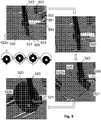
- Fig. 5 shows turning of a substrate holder 500 within a loading chamber 502 in accordance with a specific example embodiment.
- substrates 520 are received horizontally oriented into the loading chamber 502 via a loading port 501.
- the elevator (not shown) lifts or lowers the substrate holder 500 so that each substrate 520 in turn can be pushed to its place.
- the substrates 520 are supported by supports in the substrate holder 500 similarly as shown in Figs. 1 and 2 .
- the supports 522b (corresponding to supports 122b in Figs. 1 and 2 ) are partly shown in the top-left drawing of Fig. 5 .
- Hanger plates 523 are attached to a reaction chamber lid (not shown).
- the substrate holder side plates 521 are connected to the hanger plates 523 at the point of rotation centers 524 (one of which is shown in Fig. 5 ).
- the substrate holder is rotatable around the rotation axis defined by the rotation centers 524.
- An actuator pin 550 is pushed through the sidewall of the loading chamber 502 at the point of a loading chamber wall feedthrough 551.
- the shaped end plug of the actuator pin 550 is pushed into a correspondingly shaped socket in the rotation center 524 as illustrated in the top-right drawing of Fig. 5 .
- a corresponding pin (not shown) is pushed into the rotation center of the opposite side of the substrate holder 500.
- the substrate holder 500 is rotated by turning one or both of the actuator pins 550, as depicted by the arrow in the bottom-right drawing of Fig. 5 .
- the bottom-right drawing of Fig. 5 illustrates the position in which the substrate holder 500 has turned around 45 degrees, and the bottom-left drawing of Fig. 5 the position in which the substrate holder 500 has turned around 90 degrees to form a horizontal stack of vertically oriented substrates.
- the rotating action in an example embodiment is illustrated in more detail in the magnification picture set between the top-left and bottom-left drawings.
- the magnification picture set shows in black colour the rotation center 524 with the socket.
- the rotation center 524 further comprises two fins, at the interval of 90 degrees.
- the rotation center 524 is located in a hole of the hanger plate 523.
- the first fin of the rotation center 524 is in a side slot of the hanger plate hole locking the substrate holder 500 in its initial position.
- the hole is slightly larger than the rotation center 524.
- the reaction chamber elevator see Figs.
- the reaction chamber elevator lifts the hanger plates 523 with respect to the substrate holder side plates 521 so that the second fin of the rotation center 524 moves into the side slot thereby locking the substrate holder 500 into the 90 degrees turned position.
- the actuator pins may be pneumatic. Two actuator pins can support the substrate holder so that one actuator pin supports the substrate holder on a first side and the other on the opposite side.
- the actuators may be designed to be of another shape depending on the implementation.
- the loading chamber wall feedthrough 551 is a rotation feedthrough. The bearings for the rotation movement are placed on the outside of the loading chamber.
- Fig. 6 shows a side view of a deposition reactor in accordance with yet another example embodiment.
- the deposition reactor comprises a gate 670 between the loading chamber 102 and the reaction chamber 103. This may be in order to reduce cooling of the reaction chamber 103 during the loading of the substrates into the loading chamber 102 that resides on top of the reaction chamber 103.
- the gate 670 may be a gate valve.
- the gate 670 may be in a closed position during the loading of the substrates into the loading chamber 102 as depicted by the lower drawing of Fig. 6 .
- the gate 670 is opened (as depicted by the upper drawing of Fig. 6 ) to allow the loaded substrate batch to be lowered into the reaction chamber 103.
- the embodiments shown in Fig. 1 and 2 reference is made to the embodiments shown in Figs. 1 and 2 .
- a technical effect is a top loading system for a vertical flow deposition reactor in which the substrates can be loaded as horizontally oriented. Another technical effect is eliminating the need for flipping each substrate separately by flipping the whole substrate holder (especially, if the substrates are stored horizontally oriented). Another technical effect is minimizing a loading distance in a reactor cluster.
Landscapes
- Chemical & Material Sciences (AREA)
- Engineering & Computer Science (AREA)
- General Chemical & Material Sciences (AREA)
- Chemical Kinetics & Catalysis (AREA)
- Materials Engineering (AREA)
- Mechanical Engineering (AREA)
- Metallurgy (AREA)
- Organic Chemistry (AREA)
- Chemical Vapour Deposition (AREA)
- Container, Conveyance, Adherence, Positioning, Of Wafer (AREA)
- Robotics (AREA)
- Crystals, And After-Treatments Of Crystals (AREA)
Claims (14)
- Procédé comprenant :le chargement d'une pluralité de substrats (120) dans un porte-substrat (121) dans une chambre de chargement (102) d'un réacteur de dépôt pour former un empilement vertical de substrats orientés horizontalement au sein dudit porte-substrat, la chambre de chargement (102) étant sous vide ; etle pivotement du porte-substrat (121) au sein de la chambre de chargement (102) pour former un empilement horizontal de substrats orientés verticalement et abaisser le porte-substrat dans une chambre réactionnelle (103) du réacteur de dépôt pour un dépôt.
- Procédé selon la revendication 1, dans lequel le chargement comprend le déplacement de substrats (120) un à la fois par un chargeur (131) par le biais d'un orifice de chargement (101) dans la chambre de chargement (102).
- Procédé selon la revendication 1 ou 2, comprenant :la fourniture d'une barrière (670) entre la chambre de chargement (102) et la chambre réactionnelle (103), la chambre de chargement se situant au-dessus de la chambre réactionnelle.
- Procédé selon l'une quelconque des revendications précédentes, comprenant :le chargement desdits substrats (120) à partir d'un support de stockage de substrats (403) par un module d'extrémité frontale d'équipement (404) dans une station de ramassage et de retour du dispositif de chargement (405) ; etle chargement desdits substrats un à la fois à partir de la station de ramassage et de retour du dispositif de chargement (405) par le biais d'une chambre de transfert (460) dans la chambre de chargement (102).
- Procédé selon l'une quelconque des revendications précédentes, comprenant le pivotement du porte-substrat (121) par un mouvement rotatif.
- Procédé selon l'une quelconque des revendications précédentes, comprenant l'accès au porte-substrat (121) à partir d'un côté par un système d'actionnement (550) et le pivotement du porte-substrat par le système d'actionnement.
- Procédé selon l'une quelconque des revendications précédentes, comprenant :l'exposition de la pluralité de substrats (120) à des impulsions de précurseur séparées de manière temporelle dans la chambre réactionnelle (103) pour déposer un matériau sur les surfaces des substrats par des réactions de surface auto-saturantes séquentielles.
- Réacteur de dépôt, comprenant :une chambre de chargement (102) configurée pour être pompée sous vide ;une chambre réactionnelle (103) ;un chargeur (131, 431) configuré pour charger une pluralité de substrats (120) dans un porte-substrat (121) dans la chambre de chargement (102) du réacteur de dépôt pour former un empilement vertical de substrats orientés horizontalement au sein dudit port-substrat ;un mécanisme de pivotement (380a-c) configuré pour faire pivoter le porte-substrat (121) au sein de la chambre de chargement (102) pour former un empilement horizontal de substrats orientés verticalement (120) ; etun élévateur (141) configuré pour abaisser le porte-substrat (121) dans la chambre réactionnelle (103) du réacteur de dépôt pour le dépôt.
- Réacteur de dépôt selon la revendication 8, comprenant un orifice de chargement (101) et dans lequel le chargeur (131, 431) est configuré pour déplacer les substrats (120) un à la fois par le biais de l'orifice de chargement (101) dans la chambre de chargement (102).
- Réacteur de dépôt selon la revendication 8 ou 9, comprenant :une barrière (670) entre la chambre de chargement (102) et la chambre réactionnelle (103), la chambre de chargement se situant au-dessus de la chambre réactionnelle.
- Réacteur de dépôt selon l'une quelconque des revendications 8 à 10 précédentes, comprenant :un module d'extrémité frontale d'équipement (404) configuré pour charger lesdits substrats (120) à partir d'un support de stockage de substrats (403) dans une station de ramassage et de retour du dispositif de chargement (405) ; etle chargeur (131, 431) configuré pour charger lesdits substrats (120) un à la fois à partir de la station de ramassage et de retour du dispositif de chargement (405) par le biais d'une chambre de transfert (460) dans la chambre de chargement (102).
- Réacteur de dépôt selon l'une quelconque des revendications 8 à 11 précédentes, dans lequel le mécanisme de pivotement (380a-c) est configuré pour faire pivoter le porte-substrat (121) par un mouvement rotatif.
- Réacteur de dépôt selon l'une quelconque des revendications 8 à 12 précédentes, dans lequel le mécanisme de pivotement (380a-c) est configuré pour accéder au porte-substrat (121) par un côté, et pour faire pivoter le porte-substrat.
- Appareil, comprenant une pluralité de réacteurs de dépôt selon l'une quelconque des revendications 8 à 13 positionnés selon un schéma prédéterminé les uns par rapport aux autres, et le chargeur (131, 431) configuré pour charger chaque réacteur de dépôt.
Priority Applications (2)
| Application Number | Priority Date | Filing Date | Title |
|---|---|---|---|
| EP18202273.1A EP3462477A1 (fr) | 2012-11-23 | 2012-11-23 | Chargement de substrat |
| EP24170463.4A EP4379091A3 (fr) | 2012-11-23 | 2012-11-23 | Chargement de substrat |
Applications Claiming Priority (1)
| Application Number | Priority Date | Filing Date | Title |
|---|---|---|---|
| PCT/FI2012/051160 WO2014080067A1 (fr) | 2012-11-23 | 2012-11-23 | Chargement de substrat dans un réacteur ald |
Related Child Applications (2)
| Application Number | Title | Priority Date | Filing Date |
|---|---|---|---|
| EP24170463.4A Division EP4379091A3 (fr) | 2012-11-23 | 2012-11-23 | Chargement de substrat |
| EP18202273.1A Division EP3462477A1 (fr) | 2012-11-23 | 2012-11-23 | Chargement de substrat |
Publications (3)
| Publication Number | Publication Date |
|---|---|
| EP2922980A1 EP2922980A1 (fr) | 2015-09-30 |
| EP2922980A4 EP2922980A4 (fr) | 2016-07-06 |
| EP2922980B1 true EP2922980B1 (fr) | 2018-11-21 |
Family
ID=50775590
Family Applications (3)
| Application Number | Title | Priority Date | Filing Date |
|---|---|---|---|
| EP24170463.4A Pending EP4379091A3 (fr) | 2012-11-23 | 2012-11-23 | Chargement de substrat |
| EP12888893.0A Active EP2922980B1 (fr) | 2012-11-23 | 2012-11-23 | Chargement de substrat dans un réacteur ald |
| EP18202273.1A Pending EP3462477A1 (fr) | 2012-11-23 | 2012-11-23 | Chargement de substrat |
Family Applications Before (1)
| Application Number | Title | Priority Date | Filing Date |
|---|---|---|---|
| EP24170463.4A Pending EP4379091A3 (fr) | 2012-11-23 | 2012-11-23 | Chargement de substrat |
Family Applications After (1)
| Application Number | Title | Priority Date | Filing Date |
|---|---|---|---|
| EP18202273.1A Pending EP3462477A1 (fr) | 2012-11-23 | 2012-11-23 | Chargement de substrat |
Country Status (9)
| Country | Link |
|---|---|
| US (2) | US10161038B2 (fr) |
| EP (3) | EP4379091A3 (fr) |
| JP (1) | JP6240678B2 (fr) |
| KR (2) | KR102227176B1 (fr) |
| CN (1) | CN104812938B (fr) |
| RU (1) | RU2620230C2 (fr) |
| SG (1) | SG11201503227XA (fr) |
| TW (2) | TWI621734B (fr) |
| WO (1) | WO2014080067A1 (fr) |
Cited By (1)
| Publication number | Priority date | Publication date | Assignee | Title |
|---|---|---|---|---|
| WO2026041823A1 (fr) * | 2024-08-20 | 2026-02-26 | Picosun Oy | Appareil et procédé de traitement discontinu |
Families Citing this family (23)
| Publication number | Priority date | Publication date | Assignee | Title |
|---|---|---|---|---|
| US10347516B2 (en) | 2014-11-11 | 2019-07-09 | Applied Materials, Inc. | Substrate transfer chamber |
| US9520312B2 (en) * | 2014-12-19 | 2016-12-13 | Varian Semiconductor Equipment Associates, Inc. | System and method for moving workpieces between multiple vacuum environments |
| US10533251B2 (en) * | 2015-12-31 | 2020-01-14 | Lam Research Corporation | Actuator to dynamically adjust showerhead tilt in a semiconductor processing apparatus |
| US20190194809A1 (en) * | 2016-09-16 | 2019-06-27 | Picosun Oy | Apparatus and methods for atomic layer deposition |
| US11725279B2 (en) | 2017-02-08 | 2023-08-15 | Picosun Oy | Deposition or cleaning apparatus with movable structure |
| US11761082B2 (en) * | 2017-05-02 | 2023-09-19 | Picosun Oy | ALD apparatus, method and valve |
| WO2019185183A1 (fr) * | 2018-03-28 | 2019-10-03 | Applied Materials, Inc. | Appareil de traitement sous vide et procédé de traitement d'un substrat |
| EP3672040A1 (fr) * | 2018-12-17 | 2020-06-24 | Nexperia B.V. | Dispositif permettant un mouvement de rotation et de translation à l'aide d'un seul moteur ; appareil et système comprenant un tel dispositif |
| KR102733545B1 (ko) | 2019-03-19 | 2024-11-21 | 어플라이드 머티어리얼스 이탈리아 에스.알.엘. | 증착 장치, 기판 상의 증착 방법, 기판 구조 및 기판 지지부 |
| JP7292110B2 (ja) * | 2019-05-29 | 2023-06-16 | キヤノン株式会社 | 成膜装置および成膜方法 |
| EP3990680A4 (fr) * | 2019-06-25 | 2023-01-11 | Picosun Oy | Protection de face arrière de substrat |
| KR102863063B1 (ko) * | 2020-02-12 | 2025-09-22 | 에이에스엠 아이피 홀딩 비.브이. | 다중 방향 반응 챔버를 갖는 반응기 시스템 |
| KR102907141B1 (ko) | 2020-06-01 | 2026-01-05 | 삼성디스플레이 주식회사 | 기판 고정 장치, 이를 포함하는 성막 처리 설비 및 이를 이용한 성막 처리 방법 |
| RU2752059C1 (ru) * | 2020-07-14 | 2021-07-22 | Пикосан Ой | Устройство для атомно-слоевого осаждения (ald) |
| RU2748658C1 (ru) * | 2020-07-16 | 2021-05-28 | Пикосан Ой | Устройство для осаждения или очистки с подвижной конструкцией и способ его эксплуатации |
| WO2022116339A1 (fr) * | 2020-12-03 | 2022-06-09 | 无锡邑文电子科技有限公司 | Dispositif de traitement ald et procédé de traitement |
| CN113174588A (zh) * | 2021-04-26 | 2021-07-27 | 睿馨(珠海)投资发展有限公司 | 一种原子层沉积系统及沉积方法 |
| FI130021B (en) | 2021-05-10 | 2022-12-30 | Picosun Oy | Substrate processing apparatus and method |
| FI130544B (en) * | 2021-08-13 | 2023-11-08 | Beneq Oy | An atomic layer deposition apparatus and an arrangement |
| FI130543B (en) * | 2021-08-13 | 2023-11-08 | Beneq Oy | An atomic layer deposition apparatus and method |
| CN115274510A (zh) * | 2022-08-19 | 2022-11-01 | 北京北方华创微电子装备有限公司 | 一种半导体处理设备 |
| US12542256B2 (en) | 2022-11-21 | 2026-02-03 | Applied Materials, Inc. | Batch processing chambers for plasma-enhanced deposition |
| FI131961B1 (en) * | 2023-06-21 | 2026-03-12 | Picosun Oy | A thin-film deposition apparatus cluster |
Family Cites Families (28)
| Publication number | Priority date | Publication date | Assignee | Title |
|---|---|---|---|---|
| SU1093728A1 (ru) * | 1982-07-16 | 1984-05-23 | Предприятие П/Я А-7873 | Подложкодержатель |
| JP2670503B2 (ja) | 1988-04-01 | 1997-10-29 | 東京エレクトロン株式会社 | 半導体ウエハの熱処理装置 |
| JP2545591B2 (ja) | 1988-09-30 | 1996-10-23 | 国際電気株式会社 | ウェーハ処理装置 |
| JPH03125453A (ja) | 1989-10-09 | 1991-05-28 | Toshiba Corp | 半導体ウエハ移送装置 |
| WO1995030239A2 (fr) * | 1994-04-28 | 1995-11-09 | Semitool, Incorporated | Systeme de traitement de semi-conducteur a poste de reception et de chargement de conteneurs de tranches |
| JPH0817894A (ja) * | 1994-06-27 | 1996-01-19 | Dainippon Screen Mfg Co Ltd | 基板表面処理装置 |
| US6536131B2 (en) * | 1996-07-15 | 2003-03-25 | Semitool, Inc. | Wafer handling system |
| JPH11111836A (ja) * | 1997-10-02 | 1999-04-23 | Speedfam Co Ltd | 浸漬式ワーク収納方法及び装置 |
| US6110011A (en) * | 1997-11-10 | 2000-08-29 | Applied Materials, Inc. | Integrated electrodeposition and chemical-mechanical polishing tool |
| JP3827881B2 (ja) | 1999-01-29 | 2006-09-27 | 株式会社アルバック | 真空処理装置及び基板起立装置 |
| NL1017849C2 (nl) * | 2001-04-16 | 2002-10-30 | Univ Eindhoven Tech | Werkwijze en inrichting voor het deponeren van een althans ten dele kristallijne siliciumlaag op een substraat. |
| JP4033689B2 (ja) | 2002-03-01 | 2008-01-16 | 東京エレクトロン株式会社 | 液処理装置および液処理方法 |
| JP2004281613A (ja) | 2003-03-14 | 2004-10-07 | Hitachi Kokusai Electric Inc | 基板処理装置 |
| JP4319510B2 (ja) * | 2003-10-15 | 2009-08-26 | 東京エレクトロン株式会社 | 熱処理装置及び熱処理方法 |
| KR100549276B1 (ko) * | 2003-12-31 | 2006-02-03 | 주식회사 테라세미콘 | 반도체 제조장치의 기판홀더 교환장치 |
| FI121543B (fi) * | 2005-11-17 | 2010-12-31 | Beneq Oy | Järjestely ALD-reaktorin yhteydessä |
| US20090016853A1 (en) * | 2007-07-09 | 2009-01-15 | Woo Sik Yoo | In-line wafer robotic processing system |
| US10041169B2 (en) | 2008-05-27 | 2018-08-07 | Picosun Oy | System and method for loading a substrate holder carrying a batch of vertically placed substrates into an atomic layer deposition reactor |
| US8282334B2 (en) | 2008-08-01 | 2012-10-09 | Picosun Oy | Atomic layer deposition apparatus and loading methods |
| KR20100071550A (ko) * | 2008-12-19 | 2010-06-29 | 한미반도체 주식회사 | 웨이퍼 카세트 반송장치 |
| JP5476006B2 (ja) | 2009-02-13 | 2014-04-23 | 株式会社国際電気セミコンダクターサービス | 基板処理装置、基板処理装置の基板保持具の固定部及び半導体装置の製造方法 |
| JP5247528B2 (ja) * | 2009-02-23 | 2013-07-24 | 株式会社日立国際電気 | 基板処理装置、半導体装置の製造方法、基板処理方法及びガス導入手段 |
| JP5460775B2 (ja) | 2009-07-31 | 2014-04-02 | 株式会社日立国際電気 | 半導体デバイスの製造方法、半導体デバイス及び基板処理装置 |
| JP4988902B2 (ja) | 2009-07-31 | 2012-08-01 | 株式会社日立国際電気 | 半導体デバイスの製造方法及び基板処理装置 |
| US9443749B2 (en) | 2011-01-20 | 2016-09-13 | Tokyo Electron Limited | Vacuum processing apparatus |
| JP2012174763A (ja) | 2011-02-18 | 2012-09-10 | Hitachi Kokusai Electric Inc | 基板処理装置 |
| JP5885830B2 (ja) | 2011-04-07 | 2016-03-16 | ピコサン オーワイPicosun Oy | プラズマ源を有する堆積反応炉 |
| US9449862B2 (en) * | 2011-06-03 | 2016-09-20 | Tel Nexx, Inc. | Parallel single substrate processing system |
-
2012
- 2012-11-23 RU RU2015122215A patent/RU2620230C2/ru active
- 2012-11-23 CN CN201280077254.2A patent/CN104812938B/zh active Active
- 2012-11-23 KR KR1020207011539A patent/KR102227176B1/ko active Active
- 2012-11-23 JP JP2015543487A patent/JP6240678B2/ja active Active
- 2012-11-23 US US14/646,504 patent/US10161038B2/en active Active
- 2012-11-23 SG SG11201503227XA patent/SG11201503227XA/en unknown
- 2012-11-23 KR KR1020157011852A patent/KR102105070B1/ko active Active
- 2012-11-23 WO PCT/FI2012/051160 patent/WO2014080067A1/fr not_active Ceased
- 2012-11-23 EP EP24170463.4A patent/EP4379091A3/fr active Pending
- 2012-11-23 EP EP12888893.0A patent/EP2922980B1/fr active Active
- 2012-11-23 EP EP18202273.1A patent/EP3462477A1/fr active Pending
-
2013
- 2013-10-30 TW TW102139329A patent/TWI621734B/zh active
- 2013-10-30 TW TW107106000A patent/TWI706051B/zh active
-
2018
- 2018-10-19 US US16/165,303 patent/US11280001B2/en active Active
Non-Patent Citations (1)
| Title |
|---|
| None * |
Cited By (1)
| Publication number | Priority date | Publication date | Assignee | Title |
|---|---|---|---|---|
| WO2026041823A1 (fr) * | 2024-08-20 | 2026-02-26 | Picosun Oy | Appareil et procédé de traitement discontinu |
Also Published As
| Publication number | Publication date |
|---|---|
| KR20150086255A (ko) | 2015-07-27 |
| US20190048465A1 (en) | 2019-02-14 |
| EP2922980A4 (fr) | 2016-07-06 |
| CN104812938B (zh) | 2017-07-07 |
| EP4379091A3 (fr) | 2024-08-21 |
| JP6240678B2 (ja) | 2017-11-29 |
| EP2922980A1 (fr) | 2015-09-30 |
| TW201425192A (zh) | 2014-07-01 |
| KR102227176B1 (ko) | 2021-03-12 |
| KR20200045002A (ko) | 2020-04-29 |
| EP4379091A2 (fr) | 2024-06-05 |
| TWI706051B (zh) | 2020-10-01 |
| SG11201503227XA (en) | 2015-06-29 |
| RU2015122215A (ru) | 2017-01-10 |
| JP2016503462A (ja) | 2016-02-04 |
| US10161038B2 (en) | 2018-12-25 |
| WO2014080067A1 (fr) | 2014-05-30 |
| EP3462477A1 (fr) | 2019-04-03 |
| RU2620230C2 (ru) | 2017-05-23 |
| TW201827641A (zh) | 2018-08-01 |
| US11280001B2 (en) | 2022-03-22 |
| US20150299859A1 (en) | 2015-10-22 |
| TWI621734B (zh) | 2018-04-21 |
| KR102105070B1 (ko) | 2020-04-27 |
| CN104812938A (zh) | 2015-07-29 |
Similar Documents
| Publication | Publication Date | Title |
|---|---|---|
| US11280001B2 (en) | Substrate loading in an ALD reactor | |
| US5879459A (en) | Vertically-stacked process reactor and cluster tool system for atomic layer deposition | |
| US9543180B2 (en) | Apparatus and method for transporting wafers between wafer carrier and process tool under vacuum | |
| US8382088B2 (en) | Substrate processing apparatus | |
| US10431481B2 (en) | Load lock apparatus and substrate processing system | |
| US6818067B2 (en) | Processing chamber for atomic layer deposition processes | |
| KR20060017925A (ko) | 처리 장비용 더블 이중 슬롯 로드록 | |
| KR101613544B1 (ko) | 기판 처리 장치 | |
| US9716021B2 (en) | Substrate heat treatment apparatus, method of installing substrate heat treatment apparatus | |
| US20070065581A1 (en) | Substrate processing system and method | |
| US20060251499A1 (en) | Linear substrate delivery system with intermediate carousel | |
| JP6445603B2 (ja) | Ald反応炉における基板の装填 | |
| JP6920506B2 (ja) | Ald反応炉における基板の装填 | |
| JP6820900B2 (ja) | Ald反応炉における基板の装填 | |
| US20150214080A1 (en) | Substrate heat treatment apparatus, method of installing substrate heat treatment apparatus |
Legal Events
| Date | Code | Title | Description |
|---|---|---|---|
| PUAI | Public reference made under article 153(3) epc to a published international application that has entered the european phase |
Free format text: ORIGINAL CODE: 0009012 |
|
| 17P | Request for examination filed |
Effective date: 20150528 |
|
| AK | Designated contracting states |
Kind code of ref document: A1 Designated state(s): AL AT BE BG CH CY CZ DE DK EE ES FI FR GB GR HR HU IE IS IT LI LT LU LV MC MK MT NL NO PL PT RO RS SE SI SK SM TR |
|
| AX | Request for extension of the european patent |
Extension state: BA ME |
|
| DAX | Request for extension of the european patent (deleted) | ||
| RA4 | Supplementary search report drawn up and despatched (corrected) |
Effective date: 20160608 |
|
| RIC1 | Information provided on ipc code assigned before grant |
Ipc: C23C 16/455 20060101AFI20160602BHEP Ipc: C23C 16/458 20060101ALI20160602BHEP Ipc: H01L 21/677 20060101ALI20160602BHEP Ipc: H01L 21/687 20060101ALI20160602BHEP |
|
| STAA | Information on the status of an ep patent application or granted ep patent |
Free format text: STATUS: EXAMINATION IS IN PROGRESS |
|
| 17Q | First examination report despatched |
Effective date: 20170612 |
|
| GRAP | Despatch of communication of intention to grant a patent |
Free format text: ORIGINAL CODE: EPIDOSNIGR1 |
|
| STAA | Information on the status of an ep patent application or granted ep patent |
Free format text: STATUS: GRANT OF PATENT IS INTENDED |
|
| INTG | Intention to grant announced |
Effective date: 20180625 |
|
| GRAS | Grant fee paid |
Free format text: ORIGINAL CODE: EPIDOSNIGR3 |
|
| GRAA | (expected) grant |
Free format text: ORIGINAL CODE: 0009210 |
|
| STAA | Information on the status of an ep patent application or granted ep patent |
Free format text: STATUS: THE PATENT HAS BEEN GRANTED |
|
| AK | Designated contracting states |
Kind code of ref document: B1 Designated state(s): AL AT BE BG CH CY CZ DE DK EE ES FI FR GB GR HR HU IE IS IT LI LT LU LV MC MK MT NL NO PL PT RO RS SE SI SK SM TR |
|
| REG | Reference to a national code |
Ref country code: CH Ref legal event code: EP |
|
| REG | Reference to a national code |
Ref country code: IE Ref legal event code: FG4D |
|
| REG | Reference to a national code |
Ref country code: DE Ref legal event code: R096 Ref document number: 602012053949 Country of ref document: DE |
|
| REG | Reference to a national code |
Ref country code: AT Ref legal event code: REF Ref document number: 1067611 Country of ref document: AT Kind code of ref document: T Effective date: 20181215 |
|
| REG | Reference to a national code |
Ref country code: NL Ref legal event code: FP |
|
| REG | Reference to a national code |
Ref country code: SE Ref legal event code: TRGR |
|
| PG25 | Lapsed in a contracting state [announced via postgrant information from national office to epo] |
Ref country code: IS Free format text: LAPSE BECAUSE OF FAILURE TO SUBMIT A TRANSLATION OF THE DESCRIPTION OR TO PAY THE FEE WITHIN THE PRESCRIBED TIME-LIMIT Effective date: 20190321 Ref country code: NO Free format text: LAPSE BECAUSE OF FAILURE TO SUBMIT A TRANSLATION OF THE DESCRIPTION OR TO PAY THE FEE WITHIN THE PRESCRIBED TIME-LIMIT Effective date: 20190221 Ref country code: BG Free format text: LAPSE BECAUSE OF FAILURE TO SUBMIT A TRANSLATION OF THE DESCRIPTION OR TO PAY THE FEE WITHIN THE PRESCRIBED TIME-LIMIT Effective date: 20190221 Ref country code: ES Free format text: LAPSE BECAUSE OF FAILURE TO SUBMIT A TRANSLATION OF THE DESCRIPTION OR TO PAY THE FEE WITHIN THE PRESCRIBED TIME-LIMIT Effective date: 20181121 Ref country code: LT Free format text: LAPSE BECAUSE OF FAILURE TO SUBMIT A TRANSLATION OF THE DESCRIPTION OR TO PAY THE FEE WITHIN THE PRESCRIBED TIME-LIMIT Effective date: 20181121 Ref country code: LV Free format text: LAPSE BECAUSE OF FAILURE TO SUBMIT A TRANSLATION OF THE DESCRIPTION OR TO PAY THE FEE WITHIN THE PRESCRIBED TIME-LIMIT Effective date: 20181121 Ref country code: HR Free format text: LAPSE BECAUSE OF FAILURE TO SUBMIT A TRANSLATION OF THE DESCRIPTION OR TO PAY THE FEE WITHIN THE PRESCRIBED TIME-LIMIT Effective date: 20181121 |
|
| PG25 | Lapsed in a contracting state [announced via postgrant information from national office to epo] |
Ref country code: PT Free format text: LAPSE BECAUSE OF FAILURE TO SUBMIT A TRANSLATION OF THE DESCRIPTION OR TO PAY THE FEE WITHIN THE PRESCRIBED TIME-LIMIT Effective date: 20190321 Ref country code: AL Free format text: LAPSE BECAUSE OF FAILURE TO SUBMIT A TRANSLATION OF THE DESCRIPTION OR TO PAY THE FEE WITHIN THE PRESCRIBED TIME-LIMIT Effective date: 20181121 Ref country code: GR Free format text: LAPSE BECAUSE OF FAILURE TO SUBMIT A TRANSLATION OF THE DESCRIPTION OR TO PAY THE FEE WITHIN THE PRESCRIBED TIME-LIMIT Effective date: 20190222 Ref country code: RS Free format text: LAPSE BECAUSE OF FAILURE TO SUBMIT A TRANSLATION OF THE DESCRIPTION OR TO PAY THE FEE WITHIN THE PRESCRIBED TIME-LIMIT Effective date: 20181121 |
|
| PG25 | Lapsed in a contracting state [announced via postgrant information from national office to epo] |
Ref country code: DK Free format text: LAPSE BECAUSE OF FAILURE TO SUBMIT A TRANSLATION OF THE DESCRIPTION OR TO PAY THE FEE WITHIN THE PRESCRIBED TIME-LIMIT Effective date: 20181121 Ref country code: PL Free format text: LAPSE BECAUSE OF FAILURE TO SUBMIT A TRANSLATION OF THE DESCRIPTION OR TO PAY THE FEE WITHIN THE PRESCRIBED TIME-LIMIT Effective date: 20181121 Ref country code: LU Free format text: LAPSE BECAUSE OF NON-PAYMENT OF DUE FEES Effective date: 20181123 Ref country code: CZ Free format text: LAPSE BECAUSE OF FAILURE TO SUBMIT A TRANSLATION OF THE DESCRIPTION OR TO PAY THE FEE WITHIN THE PRESCRIBED TIME-LIMIT Effective date: 20181121 |
|
| REG | Reference to a national code |
Ref country code: DE Ref legal event code: R097 Ref document number: 602012053949 Country of ref document: DE |
|
| PG25 | Lapsed in a contracting state [announced via postgrant information from national office to epo] |
Ref country code: EE Free format text: LAPSE BECAUSE OF FAILURE TO SUBMIT A TRANSLATION OF THE DESCRIPTION OR TO PAY THE FEE WITHIN THE PRESCRIBED TIME-LIMIT Effective date: 20181121 Ref country code: RO Free format text: LAPSE BECAUSE OF FAILURE TO SUBMIT A TRANSLATION OF THE DESCRIPTION OR TO PAY THE FEE WITHIN THE PRESCRIBED TIME-LIMIT Effective date: 20181121 Ref country code: SK Free format text: LAPSE BECAUSE OF FAILURE TO SUBMIT A TRANSLATION OF THE DESCRIPTION OR TO PAY THE FEE WITHIN THE PRESCRIBED TIME-LIMIT Effective date: 20181121 Ref country code: MC Free format text: LAPSE BECAUSE OF FAILURE TO SUBMIT A TRANSLATION OF THE DESCRIPTION OR TO PAY THE FEE WITHIN THE PRESCRIBED TIME-LIMIT Effective date: 20181121 Ref country code: SM Free format text: LAPSE BECAUSE OF FAILURE TO SUBMIT A TRANSLATION OF THE DESCRIPTION OR TO PAY THE FEE WITHIN THE PRESCRIBED TIME-LIMIT Effective date: 20181121 |
|
| PLBE | No opposition filed within time limit |
Free format text: ORIGINAL CODE: 0009261 |
|
| STAA | Information on the status of an ep patent application or granted ep patent |
Free format text: STATUS: NO OPPOSITION FILED WITHIN TIME LIMIT |
|
| 26N | No opposition filed |
Effective date: 20190822 |
|
| PG25 | Lapsed in a contracting state [announced via postgrant information from national office to epo] |
Ref country code: SI Free format text: LAPSE BECAUSE OF FAILURE TO SUBMIT A TRANSLATION OF THE DESCRIPTION OR TO PAY THE FEE WITHIN THE PRESCRIBED TIME-LIMIT Effective date: 20181121 |
|
| PG25 | Lapsed in a contracting state [announced via postgrant information from national office to epo] |
Ref country code: MT Free format text: LAPSE BECAUSE OF NON-PAYMENT OF DUE FEES Effective date: 20181123 |
|
| PG25 | Lapsed in a contracting state [announced via postgrant information from national office to epo] |
Ref country code: TR Free format text: LAPSE BECAUSE OF FAILURE TO SUBMIT A TRANSLATION OF THE DESCRIPTION OR TO PAY THE FEE WITHIN THE PRESCRIBED TIME-LIMIT Effective date: 20181121 |
|
| REG | Reference to a national code |
Ref country code: AT Ref legal event code: UEP Ref document number: 1067611 Country of ref document: AT Kind code of ref document: T Effective date: 20181121 |
|
| PG25 | Lapsed in a contracting state [announced via postgrant information from national office to epo] |
Ref country code: MK Free format text: LAPSE BECAUSE OF NON-PAYMENT OF DUE FEES Effective date: 20181121 Ref country code: CY Free format text: LAPSE BECAUSE OF FAILURE TO SUBMIT A TRANSLATION OF THE DESCRIPTION OR TO PAY THE FEE WITHIN THE PRESCRIBED TIME-LIMIT Effective date: 20181121 Ref country code: HU Free format text: LAPSE BECAUSE OF FAILURE TO SUBMIT A TRANSLATION OF THE DESCRIPTION OR TO PAY THE FEE WITHIN THE PRESCRIBED TIME-LIMIT; INVALID AB INITIO Effective date: 20121123 |
|
| PGFP | Annual fee paid to national office [announced via postgrant information from national office to epo] |
Ref country code: GB Payment date: 20241120 Year of fee payment: 13 |
|
| PGFP | Annual fee paid to national office [announced via postgrant information from national office to epo] |
Ref country code: IE Payment date: 20241125 Year of fee payment: 13 |
|
| PGFP | Annual fee paid to national office [announced via postgrant information from national office to epo] |
Ref country code: SE Payment date: 20241120 Year of fee payment: 13 |
|
| PGFP | Annual fee paid to national office [announced via postgrant information from national office to epo] |
Ref country code: CH Payment date: 20241201 Year of fee payment: 13 |
|
| PGFP | Annual fee paid to national office [announced via postgrant information from national office to epo] |
Ref country code: NL Payment date: 20251022 Year of fee payment: 14 |
|
| PGFP | Annual fee paid to national office [announced via postgrant information from national office to epo] |
Ref country code: DE Payment date: 20251022 Year of fee payment: 14 |
|
| PGFP | Annual fee paid to national office [announced via postgrant information from national office to epo] |
Ref country code: AT Payment date: 20251024 Year of fee payment: 14 |
|
| PGFP | Annual fee paid to national office [announced via postgrant information from national office to epo] |
Ref country code: FI Payment date: 20251022 Year of fee payment: 14 Ref country code: IT Payment date: 20251022 Year of fee payment: 14 |
|
| PGFP | Annual fee paid to national office [announced via postgrant information from national office to epo] |
Ref country code: FR Payment date: 20251022 Year of fee payment: 14 |
|
| PGFP | Annual fee paid to national office [announced via postgrant information from national office to epo] |
Ref country code: BE Payment date: 20251022 Year of fee payment: 14 |