EP2924729A2 - Boîtier électronique et procédé de connexion d'une première puce à une seconde puce afin de former un boîtier électronique - Google Patents
Boîtier électronique et procédé de connexion d'une première puce à une seconde puce afin de former un boîtier électronique Download PDFInfo
- Publication number
- EP2924729A2 EP2924729A2 EP15155426.8A EP15155426A EP2924729A2 EP 2924729 A2 EP2924729 A2 EP 2924729A2 EP 15155426 A EP15155426 A EP 15155426A EP 2924729 A2 EP2924729 A2 EP 2924729A2
- Authority
- EP
- European Patent Office
- Prior art keywords
- die
- substrate
- electronic package
- cavity
- buildup layers
- Prior art date
- Legal status (The legal status is an assumption and is not a legal conclusion. Google has not performed a legal analysis and makes no representation as to the accuracy of the status listed.)
- Ceased
Links
Images


Classifications
-
- H—ELECTRICITY
- H10—SEMICONDUCTOR DEVICES; ELECTRIC SOLID-STATE DEVICES NOT OTHERWISE PROVIDED FOR
- H10W—GENERIC PACKAGES, INTERCONNECTIONS, CONNECTORS OR OTHER CONSTRUCTIONAL DETAILS OF DEVICES COVERED BY CLASS H10
- H10W90/00—Package configurations
-
- H—ELECTRICITY
- H05—ELECTRIC TECHNIQUES NOT OTHERWISE PROVIDED FOR
- H05K—PRINTED CIRCUITS; CASINGS OR CONSTRUCTIONAL DETAILS OF ELECTRIC APPARATUS; MANUFACTURE OF ASSEMBLAGES OF ELECTRICAL COMPONENTS
- H05K1/00—Printed circuits
- H05K1/18—Printed circuits structurally associated with non-printed electric components
- H05K1/182—Printed circuits structurally associated with non-printed electric components associated with components mounted in printed circuit boards [PCB], e.g. insert-mounted components [IMC]
- H05K1/183—Printed circuits structurally associated with non-printed electric components associated with components mounted in printed circuit boards [PCB], e.g. insert-mounted components [IMC] associated with components mounted in and supported by recessed areas of the PCBs
-
- H—ELECTRICITY
- H05—ELECTRIC TECHNIQUES NOT OTHERWISE PROVIDED FOR
- H05K—PRINTED CIRCUITS; CASINGS OR CONSTRUCTIONAL DETAILS OF ELECTRIC APPARATUS; MANUFACTURE OF ASSEMBLAGES OF ELECTRICAL COMPONENTS
- H05K1/00—Printed circuits
- H05K1/18—Printed circuits structurally associated with non-printed electric components
- H05K1/182—Printed circuits structurally associated with non-printed electric components associated with components mounted in printed circuit boards [PCB], e.g. insert-mounted components [IMC]
- H05K1/185—Printed circuits structurally associated with non-printed electric components associated with components mounted in printed circuit boards [PCB], e.g. insert-mounted components [IMC] associated with components encapsulated in the insulating substrate of the PCBs; associated with components incorporated in internal layers of multilayer circuit boards
- H05K1/186—Printed circuits structurally associated with non-printed electric components associated with components mounted in printed circuit boards [PCB], e.g. insert-mounted components [IMC] associated with components encapsulated in the insulating substrate of the PCBs; associated with components incorporated in internal layers of multilayer circuit boards manufactured by mounting on or connecting to patterned circuits before or during embedding
-
- H—ELECTRICITY
- H10—SEMICONDUCTOR DEVICES; ELECTRIC SOLID-STATE DEVICES NOT OTHERWISE PROVIDED FOR
- H10W—GENERIC PACKAGES, INTERCONNECTIONS, CONNECTORS OR OTHER CONSTRUCTIONAL DETAILS OF DEVICES COVERED BY CLASS H10
- H10W20/00—Interconnections in chips, wafers or substrates
- H10W20/01—Manufacture or treatment
-
- H—ELECTRICITY
- H10—SEMICONDUCTOR DEVICES; ELECTRIC SOLID-STATE DEVICES NOT OTHERWISE PROVIDED FOR
- H10W—GENERIC PACKAGES, INTERCONNECTIONS, CONNECTORS OR OTHER CONSTRUCTIONAL DETAILS OF DEVICES COVERED BY CLASS H10
- H10W20/00—Interconnections in chips, wafers or substrates
- H10W20/40—Interconnections external to wafers or substrates, e.g. back-end-of-line [BEOL] metallisations or vias connecting to gate electrodes
- H10W20/41—Interconnections external to wafers or substrates, e.g. back-end-of-line [BEOL] metallisations or vias connecting to gate electrodes characterised by their conductive parts
- H10W20/42—Vias, e.g. via plugs
-
- H—ELECTRICITY
- H10—SEMICONDUCTOR DEVICES; ELECTRIC SOLID-STATE DEVICES NOT OTHERWISE PROVIDED FOR
- H10W—GENERIC PACKAGES, INTERCONNECTIONS, CONNECTORS OR OTHER CONSTRUCTIONAL DETAILS OF DEVICES COVERED BY CLASS H10
- H10W70/00—Package substrates; Interposers; Redistribution layers [RDL]
- H10W70/01—Manufacture or treatment
- H10W70/05—Manufacture or treatment of insulating or insulated package substrates, or of interposers, or of redistribution layers
- H10W70/08—Manufacture or treatment of insulating or insulated package substrates, or of interposers, or of redistribution layers by depositing layers on the chip or wafer, e.g. "chip-first" RDLs
- H10W70/09—Manufacture or treatment of insulating or insulated package substrates, or of interposers, or of redistribution layers by depositing layers on the chip or wafer, e.g. "chip-first" RDLs extending onto an encapsulation that laterally surrounds the chip or wafer, e.g. fan-out wafer level package [FOWLP] RDLs
-
- H—ELECTRICITY
- H10—SEMICONDUCTOR DEVICES; ELECTRIC SOLID-STATE DEVICES NOT OTHERWISE PROVIDED FOR
- H10W—GENERIC PACKAGES, INTERCONNECTIONS, CONNECTORS OR OTHER CONSTRUCTIONAL DETAILS OF DEVICES COVERED BY CLASS H10
- H10W70/00—Package substrates; Interposers; Redistribution layers [RDL]
- H10W70/60—Insulating or insulated package substrates; Interposers; Redistribution layers
- H10W70/611—Insulating or insulated package substrates; Interposers; Redistribution layers for connecting multiple chips together
-
- H—ELECTRICITY
- H10—SEMICONDUCTOR DEVICES; ELECTRIC SOLID-STATE DEVICES NOT OTHERWISE PROVIDED FOR
- H10W—GENERIC PACKAGES, INTERCONNECTIONS, CONNECTORS OR OTHER CONSTRUCTIONAL DETAILS OF DEVICES COVERED BY CLASS H10
- H10W70/00—Package substrates; Interposers; Redistribution layers [RDL]
- H10W70/60—Insulating or insulated package substrates; Interposers; Redistribution layers
- H10W70/611—Insulating or insulated package substrates; Interposers; Redistribution layers for connecting multiple chips together
- H10W70/614—Insulating or insulated package substrates; Interposers; Redistribution layers for connecting multiple chips together the multiple chips being integrally enclosed
-
- H—ELECTRICITY
- H10—SEMICONDUCTOR DEVICES; ELECTRIC SOLID-STATE DEVICES NOT OTHERWISE PROVIDED FOR
- H10W—GENERIC PACKAGES, INTERCONNECTIONS, CONNECTORS OR OTHER CONSTRUCTIONAL DETAILS OF DEVICES COVERED BY CLASS H10
- H10W70/00—Package substrates; Interposers; Redistribution layers [RDL]
- H10W70/60—Insulating or insulated package substrates; Interposers; Redistribution layers
- H10W70/62—Insulating or insulated package substrates; Interposers; Redistribution layers characterised by their interconnections
- H10W70/65—Shapes or dispositions of interconnections
-
- H—ELECTRICITY
- H10—SEMICONDUCTOR DEVICES; ELECTRIC SOLID-STATE DEVICES NOT OTHERWISE PROVIDED FOR
- H10W—GENERIC PACKAGES, INTERCONNECTIONS, CONNECTORS OR OTHER CONSTRUCTIONAL DETAILS OF DEVICES COVERED BY CLASS H10
- H10W70/00—Package substrates; Interposers; Redistribution layers [RDL]
- H10W70/60—Insulating or insulated package substrates; Interposers; Redistribution layers
- H10W70/67—Insulating or insulated package substrates; Interposers; Redistribution layers characterised by their insulating layers or insulating parts
- H10W70/68—Shapes or dispositions thereof
-
- H—ELECTRICITY
- H10—SEMICONDUCTOR DEVICES; ELECTRIC SOLID-STATE DEVICES NOT OTHERWISE PROVIDED FOR
- H10W—GENERIC PACKAGES, INTERCONNECTIONS, CONNECTORS OR OTHER CONSTRUCTIONAL DETAILS OF DEVICES COVERED BY CLASS H10
- H10W74/00—Encapsulations, e.g. protective coatings
- H10W74/01—Manufacture or treatment
-
- H—ELECTRICITY
- H10—SEMICONDUCTOR DEVICES; ELECTRIC SOLID-STATE DEVICES NOT OTHERWISE PROVIDED FOR
- H10W—GENERIC PACKAGES, INTERCONNECTIONS, CONNECTORS OR OTHER CONSTRUCTIONAL DETAILS OF DEVICES COVERED BY CLASS H10
- H10W74/00—Encapsulations, e.g. protective coatings
- H10W74/10—Encapsulations, e.g. protective coatings characterised by their shape or disposition
- H10W74/111—Encapsulations, e.g. protective coatings characterised by their shape or disposition the semiconductor body being completely enclosed
- H10W74/127—Encapsulations, e.g. protective coatings characterised by their shape or disposition the semiconductor body being completely enclosed characterised by arrangements for sealing or adhesion
-
- H—ELECTRICITY
- H10—SEMICONDUCTOR DEVICES; ELECTRIC SOLID-STATE DEVICES NOT OTHERWISE PROVIDED FOR
- H10W—GENERIC PACKAGES, INTERCONNECTIONS, CONNECTORS OR OTHER CONSTRUCTIONAL DETAILS OF DEVICES COVERED BY CLASS H10
- H10W74/00—Encapsulations, e.g. protective coatings
- H10W74/10—Encapsulations, e.g. protective coatings characterised by their shape or disposition
- H10W74/131—Encapsulations, e.g. protective coatings characterised by their shape or disposition the semiconductor body being only partially enclosed
-
- H—ELECTRICITY
- H10—SEMICONDUCTOR DEVICES; ELECTRIC SOLID-STATE DEVICES NOT OTHERWISE PROVIDED FOR
- H10W—GENERIC PACKAGES, INTERCONNECTIONS, CONNECTORS OR OTHER CONSTRUCTIONAL DETAILS OF DEVICES COVERED BY CLASS H10
- H10W99/00—Subject matter not provided for in other groups of this subclass
-
- H—ELECTRICITY
- H10—SEMICONDUCTOR DEVICES; ELECTRIC SOLID-STATE DEVICES NOT OTHERWISE PROVIDED FOR
- H10W—GENERIC PACKAGES, INTERCONNECTIONS, CONNECTORS OR OTHER CONSTRUCTIONAL DETAILS OF DEVICES COVERED BY CLASS H10
- H10W70/00—Package substrates; Interposers; Redistribution layers [RDL]
- H10W70/60—Insulating or insulated package substrates; Interposers; Redistribution layers
- H10W70/62—Insulating or insulated package substrates; Interposers; Redistribution layers characterised by their interconnections
- H10W70/63—Vias, e.g. via plugs
-
- H—ELECTRICITY
- H10—SEMICONDUCTOR DEVICES; ELECTRIC SOLID-STATE DEVICES NOT OTHERWISE PROVIDED FOR
- H10W—GENERIC PACKAGES, INTERCONNECTIONS, CONNECTORS OR OTHER CONSTRUCTIONAL DETAILS OF DEVICES COVERED BY CLASS H10
- H10W70/00—Package substrates; Interposers; Redistribution layers [RDL]
- H10W70/60—Insulating or insulated package substrates; Interposers; Redistribution layers
- H10W70/67—Insulating or insulated package substrates; Interposers; Redistribution layers characterised by their insulating layers or insulating parts
- H10W70/68—Shapes or dispositions thereof
- H10W70/682—Shapes or dispositions thereof comprising holes having chips therein
-
- H—ELECTRICITY
- H10—SEMICONDUCTOR DEVICES; ELECTRIC SOLID-STATE DEVICES NOT OTHERWISE PROVIDED FOR
- H10W—GENERIC PACKAGES, INTERCONNECTIONS, CONNECTORS OR OTHER CONSTRUCTIONAL DETAILS OF DEVICES COVERED BY CLASS H10
- H10W72/00—Interconnections or connectors in packages
- H10W72/071—Connecting or disconnecting
- H10W72/072—Connecting or disconnecting of bump connectors
-
- H—ELECTRICITY
- H10—SEMICONDUCTOR DEVICES; ELECTRIC SOLID-STATE DEVICES NOT OTHERWISE PROVIDED FOR
- H10W—GENERIC PACKAGES, INTERCONNECTIONS, CONNECTORS OR OTHER CONSTRUCTIONAL DETAILS OF DEVICES COVERED BY CLASS H10
- H10W72/00—Interconnections or connectors in packages
- H10W72/071—Connecting or disconnecting
- H10W72/072—Connecting or disconnecting of bump connectors
- H10W72/07202—Connecting or disconnecting of bump connectors using auxiliary members
- H10W72/07204—Connecting or disconnecting of bump connectors using auxiliary members using temporary auxiliary members, e.g. sacrificial coatings
- H10W72/07207—Temporary substrates, e.g. removable substrates
-
- H—ELECTRICITY
- H10—SEMICONDUCTOR DEVICES; ELECTRIC SOLID-STATE DEVICES NOT OTHERWISE PROVIDED FOR
- H10W—GENERIC PACKAGES, INTERCONNECTIONS, CONNECTORS OR OTHER CONSTRUCTIONAL DETAILS OF DEVICES COVERED BY CLASS H10
- H10W72/00—Interconnections or connectors in packages
- H10W72/071—Connecting or disconnecting
- H10W72/072—Connecting or disconnecting of bump connectors
- H10W72/07231—Techniques
- H10W72/07232—Compression bonding, e.g. thermocompression bonding
-
- H—ELECTRICITY
- H10—SEMICONDUCTOR DEVICES; ELECTRIC SOLID-STATE DEVICES NOT OTHERWISE PROVIDED FOR
- H10W—GENERIC PACKAGES, INTERCONNECTIONS, CONNECTORS OR OTHER CONSTRUCTIONAL DETAILS OF DEVICES COVERED BY CLASS H10
- H10W72/00—Interconnections or connectors in packages
- H10W72/071—Connecting or disconnecting
- H10W72/073—Connecting or disconnecting of die-attach connectors
-
- H—ELECTRICITY
- H10—SEMICONDUCTOR DEVICES; ELECTRIC SOLID-STATE DEVICES NOT OTHERWISE PROVIDED FOR
- H10W—GENERIC PACKAGES, INTERCONNECTIONS, CONNECTORS OR OTHER CONSTRUCTIONAL DETAILS OF DEVICES COVERED BY CLASS H10
- H10W72/00—Interconnections or connectors in packages
- H10W72/071—Connecting or disconnecting
- H10W72/073—Connecting or disconnecting of die-attach connectors
- H10W72/07302—Connecting or disconnecting of die-attach connectors using an auxiliary member
- H10W72/07304—Connecting or disconnecting of die-attach connectors using an auxiliary member the auxiliary member being temporary, e.g. a sacrificial coating
- H10W72/07307—Connecting or disconnecting of die-attach connectors using an auxiliary member the auxiliary member being temporary, e.g. a sacrificial coating the auxiliary member being a temporary substrate, e.g. a removable substrate
-
- H—ELECTRICITY
- H10—SEMICONDUCTOR DEVICES; ELECTRIC SOLID-STATE DEVICES NOT OTHERWISE PROVIDED FOR
- H10W—GENERIC PACKAGES, INTERCONNECTIONS, CONNECTORS OR OTHER CONSTRUCTIONAL DETAILS OF DEVICES COVERED BY CLASS H10
- H10W72/00—Interconnections or connectors in packages
- H10W72/071—Connecting or disconnecting
- H10W72/073—Connecting or disconnecting of die-attach connectors
- H10W72/07331—Connecting techniques
- H10W72/07337—Connecting techniques using a polymer adhesive, e.g. an adhesive based on silicone or epoxy
- H10W72/07338—Connecting techniques using a polymer adhesive, e.g. an adhesive based on silicone or epoxy hardening the adhesive by curing, e.g. thermosetting
-
- H—ELECTRICITY
- H10—SEMICONDUCTOR DEVICES; ELECTRIC SOLID-STATE DEVICES NOT OTHERWISE PROVIDED FOR
- H10W—GENERIC PACKAGES, INTERCONNECTIONS, CONNECTORS OR OTHER CONSTRUCTIONAL DETAILS OF DEVICES COVERED BY CLASS H10
- H10W72/00—Interconnections or connectors in packages
- H10W72/20—Bump connectors, e.g. solder bumps or copper pillars; Dummy bumps; Thermal bumps
- H10W72/29—Bond pads specially adapted therefor
-
- H—ELECTRICITY
- H10—SEMICONDUCTOR DEVICES; ELECTRIC SOLID-STATE DEVICES NOT OTHERWISE PROVIDED FOR
- H10W—GENERIC PACKAGES, INTERCONNECTIONS, CONNECTORS OR OTHER CONSTRUCTIONAL DETAILS OF DEVICES COVERED BY CLASS H10
- H10W72/00—Interconnections or connectors in packages
- H10W72/30—Die-attach connectors
- H10W72/351—Materials of die-attach connectors
- H10W72/353—Materials of die-attach connectors not comprising solid metals or solid metalloids, e.g. ceramics
- H10W72/354—Materials of die-attach connectors not comprising solid metals or solid metalloids, e.g. ceramics comprising polymers
-
- H—ELECTRICITY
- H10—SEMICONDUCTOR DEVICES; ELECTRIC SOLID-STATE DEVICES NOT OTHERWISE PROVIDED FOR
- H10W—GENERIC PACKAGES, INTERCONNECTIONS, CONNECTORS OR OTHER CONSTRUCTIONAL DETAILS OF DEVICES COVERED BY CLASS H10
- H10W72/00—Interconnections or connectors in packages
- H10W72/823—Interconnections through encapsulations, e.g. pillars through molded resin on a lateral side a chip
-
- H—ELECTRICITY
- H10—SEMICONDUCTOR DEVICES; ELECTRIC SOLID-STATE DEVICES NOT OTHERWISE PROVIDED FOR
- H10W—GENERIC PACKAGES, INTERCONNECTIONS, CONNECTORS OR OTHER CONSTRUCTIONAL DETAILS OF DEVICES COVERED BY CLASS H10
- H10W72/00—Interconnections or connectors in packages
- H10W72/90—Bond pads, in general
- H10W72/941—Dispositions of bond pads
- H10W72/9413—Dispositions of bond pads on encapsulations
-
- H—ELECTRICITY
- H10—SEMICONDUCTOR DEVICES; ELECTRIC SOLID-STATE DEVICES NOT OTHERWISE PROVIDED FOR
- H10W—GENERIC PACKAGES, INTERCONNECTIONS, CONNECTORS OR OTHER CONSTRUCTIONAL DETAILS OF DEVICES COVERED BY CLASS H10
- H10W74/00—Encapsulations, e.g. protective coatings
- H10W74/10—Encapsulations, e.g. protective coatings characterised by their shape or disposition
- H10W74/131—Encapsulations, e.g. protective coatings characterised by their shape or disposition the semiconductor body being only partially enclosed
- H10W74/142—Encapsulations, e.g. protective coatings characterised by their shape or disposition the semiconductor body being only partially enclosed the encapsulations exposing the passive side of the semiconductor body
-
- H—ELECTRICITY
- H10—SEMICONDUCTOR DEVICES; ELECTRIC SOLID-STATE DEVICES NOT OTHERWISE PROVIDED FOR
- H10W—GENERIC PACKAGES, INTERCONNECTIONS, CONNECTORS OR OTHER CONSTRUCTIONAL DETAILS OF DEVICES COVERED BY CLASS H10
- H10W74/00—Encapsulations, e.g. protective coatings
- H10W74/10—Encapsulations, e.g. protective coatings characterised by their shape or disposition
- H10W74/15—Encapsulations, e.g. protective coatings characterised by their shape or disposition on active surfaces of flip-chip devices, e.g. underfills
-
- H—ELECTRICITY
- H10—SEMICONDUCTOR DEVICES; ELECTRIC SOLID-STATE DEVICES NOT OTHERWISE PROVIDED FOR
- H10W—GENERIC PACKAGES, INTERCONNECTIONS, CONNECTORS OR OTHER CONSTRUCTIONAL DETAILS OF DEVICES COVERED BY CLASS H10
- H10W90/00—Package configurations
- H10W90/20—Configurations of stacked chips
-
- H—ELECTRICITY
- H10—SEMICONDUCTOR DEVICES; ELECTRIC SOLID-STATE DEVICES NOT OTHERWISE PROVIDED FOR
- H10W—GENERIC PACKAGES, INTERCONNECTIONS, CONNECTORS OR OTHER CONSTRUCTIONAL DETAILS OF DEVICES COVERED BY CLASS H10
- H10W90/00—Package configurations
- H10W90/20—Configurations of stacked chips
- H10W90/22—Configurations of stacked chips the stacked chips being on both top and bottom sides of a package substrate, interposer or RDL
-
- H—ELECTRICITY
- H10—SEMICONDUCTOR DEVICES; ELECTRIC SOLID-STATE DEVICES NOT OTHERWISE PROVIDED FOR
- H10W—GENERIC PACKAGES, INTERCONNECTIONS, CONNECTORS OR OTHER CONSTRUCTIONAL DETAILS OF DEVICES COVERED BY CLASS H10
- H10W90/00—Package configurations
- H10W90/20—Configurations of stacked chips
- H10W90/297—Configurations of stacked chips characterised by the through-semiconductor vias [TSVs] in the stacked chips
-
- H—ELECTRICITY
- H10—SEMICONDUCTOR DEVICES; ELECTRIC SOLID-STATE DEVICES NOT OTHERWISE PROVIDED FOR
- H10W—GENERIC PACKAGES, INTERCONNECTIONS, CONNECTORS OR OTHER CONSTRUCTIONAL DETAILS OF DEVICES COVERED BY CLASS H10
- H10W90/00—Package configurations
- H10W90/701—Package configurations characterised by the relative positions of pads or connectors relative to package parts
- H10W90/721—Package configurations characterised by the relative positions of pads or connectors relative to package parts of bump connectors
- H10W90/722—Package configurations characterised by the relative positions of pads or connectors relative to package parts of bump connectors between stacked chips
-
- H—ELECTRICITY
- H10—SEMICONDUCTOR DEVICES; ELECTRIC SOLID-STATE DEVICES NOT OTHERWISE PROVIDED FOR
- H10W—GENERIC PACKAGES, INTERCONNECTIONS, CONNECTORS OR OTHER CONSTRUCTIONAL DETAILS OF DEVICES COVERED BY CLASS H10
- H10W90/00—Package configurations
- H10W90/701—Package configurations characterised by the relative positions of pads or connectors relative to package parts
- H10W90/721—Package configurations characterised by the relative positions of pads or connectors relative to package parts of bump connectors
- H10W90/724—Package configurations characterised by the relative positions of pads or connectors relative to package parts of bump connectors between a chip and a stacked insulating package substrate, interposer or RDL
-
- H—ELECTRICITY
- H10—SEMICONDUCTOR DEVICES; ELECTRIC SOLID-STATE DEVICES NOT OTHERWISE PROVIDED FOR
- H10W—GENERIC PACKAGES, INTERCONNECTIONS, CONNECTORS OR OTHER CONSTRUCTIONAL DETAILS OF DEVICES COVERED BY CLASS H10
- H10W90/00—Package configurations
- H10W90/701—Package configurations characterised by the relative positions of pads or connectors relative to package parts
- H10W90/731—Package configurations characterised by the relative positions of pads or connectors relative to package parts of die-attach connectors
- H10W90/732—Package configurations characterised by the relative positions of pads or connectors relative to package parts of die-attach connectors between stacked chips
-
- H—ELECTRICITY
- H10—SEMICONDUCTOR DEVICES; ELECTRIC SOLID-STATE DEVICES NOT OTHERWISE PROVIDED FOR
- H10W—GENERIC PACKAGES, INTERCONNECTIONS, CONNECTORS OR OTHER CONSTRUCTIONAL DETAILS OF DEVICES COVERED BY CLASS H10
- H10W90/00—Package configurations
- H10W90/701—Package configurations characterised by the relative positions of pads or connectors relative to package parts
- H10W90/731—Package configurations characterised by the relative positions of pads or connectors relative to package parts of die-attach connectors
- H10W90/734—Package configurations characterised by the relative positions of pads or connectors relative to package parts of die-attach connectors between a chip and a stacked insulating package substrate, interposer or RDL
Definitions
- Embodiments described herein generally relate to an electronic package and a method of connecting a first die to another die to form an electronic package.
- PoP configuration package-on-package
- FC flip-chip
- PoP architectures are often undesirably associated with more circuitous electric paths between the dice in the overall PoP architecture.
- Another known package type relates to die embedding.
- One difficulty associated with embedding multiple dice relates to aligning embedded multiple dice into the same electronic package.
- the difficulties related to aligning multiple embedded dice is due in part to potential complications associated with producing the fine alignment that is necessary between the conductor patterns of multiple embedded dice that are in the same electronic package.
- Orientation terminology such as “horizontal,” as used in this application is defined with respect to a plane parallel to the conventional plane or surface of a wafer or substrate, regardless of the orientation of the wafer or substrate.
- the term “vertical” refers to a direction perpendicular to the horizontal as defined above.
- Prepositions such as “on,” “side” (as in “sidewall”), “higher,” “lower,” “over,” and “under” are defined with respect to the conventional plane or surface being on the top surface of the wafer or substrate, regardless of the orientation of the wafer or substrate.
- the electronic packages and methods described herein may serve to improve the alignment between dice in multi-chip packages (MCPs) as well as the placement of one or more dice relative to the rest of the electronic package.
- MCPs multi-chip packages
- the alignment between dice may be improved by aligning additional dice to an already existing conductor pattern that exists in cavities which are created during fabrication of the electronic packages.
- MCPs multi-chip packages
- Other example electronic packages and/or products include stacked DRAM, CPU/PCH combinations.
- Examples for the mobile segment include the package integration of the Digital Baseband chip, and potentially integrated PMIC.
- the electronic packages and methods described herein may offer much more direct paths between MCP dice.
- the electronic packages and methods described herein may also bring at least one non-embedded die into the electronic package through the creation of a cavity in the electronic package and subsequent attachment of at least one non-embedded die within the cavity (e.g., through TCB).
- the electronic packages and methods described herein may also be incorporated into electronic packages for products where z-height is at a premium and various chips can advantageously combined on the same package.
- Various flexible manufacturing strategies may also be developed where different types of chips could be added to the MCP depending on the desired type of electronic package.
- an embedded die routing test may be done on a package level before committing additional dice to the MCP.
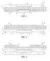
- FIG. 1 illustrates an example electronic package 10.
- the electronic package 10 includes a substrate 11 that includes a plurality of buildup layers 12A, 12B, 12C.
- a first die 13 is embedded in one of the buildup layers 12A on one side 15 of the substrate 11.
- a second die 16 is bonded to the substrate 11 within a cavity 17 on an opposing side 18 of the substrate 11.
- the first die 13 and the second die 16 may be electrically connected to conductors within the plurality of buildup layers 12A, 12B, 12C.
- the type, size and configuration of each of the first die 13 and the second die 16 that are included in the electronic package 10 will depend in part on the overall desired configuration and function of the electronic package 10.
- the second die 16 may be attached to conductors within one of the buildup layers 12B by thermal compression bonding. It should be noted that the second die 16 may be attached to conductors within one of the buildup layers 12B by any bonding method that is known now or discovered in the future. The manner in which the second die 16 is bonded to the substrate 11 will depend in part on cost, manufacturing considerations and the functionality associated with fabricating the electronic package 10 (among other factors).
- the example electronic package 10 may further include an underfill 19 between the second die 16 and the buildup layer 12B that includes the conductors that are thermal compression bonded to the second die 16.
- the underfill 19 may be formed of an epoxy-like material, or any other material that is known now or discovered in the future. The type of material that is used for the underfill 19 will depend in part on cost, manufacturing considerations and the functionality associated with fabricating the electronic package 10 (among other factors).
- FIG. 7 is a flow diagram illustrating a method [700] of connecting a first die to a second die to form an electronic package 10 (see FIG. 1 ).
- the method [700] includes [710] attaching a first die 13 to a core C and [720] fabricating a substrate 11 onto the core C.
- the substrate includes 11 a plurality of buildup layers 12A, 12B, 12C.
- the first die 13 is embedded in one of the buildup layers 12A on one side 15 of the substrate 11 (see, e.g., FIG. 2 ).
- attaching the first die 13 to the core C may include attaching the first die 13 within a cavity 20 in the core C in order to embed the first die 13 in one of the buildup layers 12A on the one side 15 of the substrate 11.
- the degree which the first die 13 is embedded in the substrate 11 will depend in part on cost, configuration, manufacturing considerations and functionality associated with fabricating the electronic package 10 (among other factors).
- the method [700] further includes [730] creating a cavity 17 in another of the buildup layers 12C on an opposing side 18 of the substrate 11 (see, e.g., FIG. 3 ) and [740] attaching a second die 16 to the substrate 11 within the cavity 17 (see, e.g., FIG. 4 ).
- [740] attaching the second die 16 to the substrate 11 within the cavity 17 may include attaching the second die 16 using thermal compression bonding (or any other type of bonding).
- the cavity may be created in any number of ways (e.g. laser drill routing).
- the cavity 17 on the opposing side 18 of the substrate 11 to the embedded first die 13 may be created in such a way as to provide access to the underlying conductor pattern in another of the buildup layers 12B.
- the second die 16 may be attached by thermal compression bonding (or any other type of bonding).
- the method [700] may further include [750] filling an area between the second die 16 and the substrate 11 with an underfill 19 (see, e.g., FIG. 5 ), and [760] curing the underfill in the electronic package 10.
- the appropriate curing process may be based in part on the types of materials and components that are used in the electronic package 10 as well as the associated manufacturing costs (among other factors).
- the method [700] may further include [770] removing the core C from the first die 16 and the substrate 11 (see, e.g., FIG. 6 ).
- the core C may be removed from the first die 16 and the substrate 11 by using a peel-enabled core, although it should be noted that any process may be used to remove the core C.
- FIG. 8 illustrates another example electronic package 80.
- the electronic package 80 includes a substrate 81 that includes a plurality of buildup layers 82A, 82B, 82C.
- a first die 83 is embedded in one of the buildup layers 82A on one side 85 of the substrate 81.
- the first die 83 may be embedded to any depth within the electronic package 10 such that the first dies engages conductive layers within any of the plurality of buildup layers 82A82B, 82C.
- a second die 86 is bonded to the substrate 81 within a cavity 87 on the same side 85 of the substrate 81.
- the first die 83 and the second die 86 may be connected to conductors within any of the plurality of buildup layers 82A, 82B, 82C.
- depth of the cavity 87 may vary such that the second die 86 engages conductive layers within any of the plurality of buildup layers 82A82B, 82C depending on the depth of the cavity 87.
- the type, size and configuration of each of the first die 83 and the second die 86 that are included in the electronic package 80 will depend in part on the overall desired configuration and function of the electronic package 80.
- the second die 86 may be attached to conductors within one of the buildup layers 82B by thermal compression bonding. It should be noted that the second die 86 may be attached to conductors within one of the buildup layers 82B by any bonding method that is known now or discovered in the future. The manner in which the second die 86 is bonded to the substrate 81 will depend in part on cost, manufacturing considerations and the functionality associated with fabricating the electronic package 80 (among other factors).
- the example electronic package 80 may further include an underfill 89 between the second die 86 and the buildup layer 82B that includes the conductors that are thermal compression bonded to the second die 86.
- the underfill 89 may be formed of an epoxy-like material, or any other material that is known now or discovered in the future. The type of material that is used for the underfill 89 will depend in part on cost, manufacturing considerations and the functionality associated with fabricating the electronic package 80 (among other factors).
- FIG. 9 illustrates another example form of the electronic package 80 shown in FIG. 8 .
- the electronic package 80 may further include a third die 93 that is bonded to the substrate 81 within a cavity 97 on an opposing side 88 of the substrate 81.
- the first die 83 and the second die 86 may be electrically connected to the third die 93 through conductors within the plurality of buildup layers 82A, 82B, 82C.
- the example electronic package 80 may further include an underfill 99 within the cavity 97 between the third die 93 and the substrate 81 that includes the conductors that are thermal compression bonded to the third die 93.
- FIG. 15 is a flow diagram illustrating a method [1500] of connecting a first die to a second die to form an electronic package 80 (see FIG. 8 ).
- the method [1500] includes [1510] attaching a first die 83 to a core C and [1520] fabricating a substrate 81 onto the core C.
- the substrate includes 81 a plurality of buildup layers 82A, 82B, 82C.
- the first die 83 is embedded in one of the buildup layers 82A on one side 85 of the substrate 81 (see, e.g., FIG. 10 ).
- attaching the first die 83 to the core C may include attaching the first die 83 within a cavity 90 in the core C in order to embed the first die 83 in one of the buildup layers 82A on the one side 85 of the substrate 81.
- the degree which the first die 83 is embedded in the substrate 81 will depend in part on cost, configuration, manufacturing considerations and functionality associated with fabricating the electronic package 80 (among other factors).
- the method [1500] may further include [1530] removing the core C from the first die 86 and the substrate 81 (see, e.g., FIG. 11 ).
- the core C may be removed from the first die 86 and the substrate 81 by using a peelable core, although it should be noted that any process may be used to remove the core C.
- the method [1500] further includes [1540] creating a cavity 87 in the buildup layer 82A that is on the same side 85 of the substrate 81 as the first die 83 (see, e.g., FIG. 12 ) and [1550] attaching a second die 86 to the substrate 81 within the cavity 87 (see, e.g., FIG. 13 ).
- attaching the second die 86 to the substrate 81 within the cavity 87 may include attaching the second die 86 using thermal compression bonding (or any other type of bonding).
- the cavity may be created in any number of ways (e.g. laser drill routing) to many possible depths depending on the overall design of the electronic package.
- the cavity 87 that is on the same side 85 of the substrate 81 as the embedded first die 83 may be created in such a way as to provide access to the underlying conductor pattern in any of the buildup layers 82A, 82B, 82C depending on the depth of the cavity 87.
- the second die 86 may be attached by thermal compression bonding (or any other type of bonding).
- the method [1500] may further include [1560] filling an area between the second die 86 and the substrate 81 with an underfill 89 (see, e.g., FIG. 14 ), and [1570] curing the underfill in the electronic package 80.
- the appropriate curing process may be based in part on the types of materials and components that are used in the electronic package 80 as well as the associated manufacturing costs (among other factors).
- the method [1500] may further include [1580] creating a cavity 97 in the buildup layer 82C on an opposing side 88 of the substrate 81 to the first die 83 and the second die 86.
- the method [1500] may further include [1590] attaching a third die 93 to the substrate 81 within the cavity 97 on the opposing side 88 of the substrate 81 to the first die 83 and the second die 86 (see, e.g., FIG. 9 ).
- the method [1500] may further include inserting an underfill 99 within the cavity 97 between the third die 93 and the substrate 81.
- FIG. 16 is a block diagram of an electronic device 1600 incorporating at least one electronic package and/or method described herein.
- Electronic device 1600 is merely one example of an electronic system in which embodiments of the present invention may be used.
- Examples of electronic devices 1600 include, but are not limited to personal computers, tablet computers, mobile telephones, game devices, MP3 or other digital music players, etc.
- electronic device 1600 comprises a data processing system that includes a system bus 1602 to couple the various components of the system.
- System bus 1602 provides communications links among the various components of the electronic device 1600 and can be implemented as a single bus, as a combination of busses, or in any other suitable manner.
- An electronic package 1610 is coupled to system bus 1602.
- the electronic package 1610 can include any circuit or combination of circuits.
- the electronic package 1610 includes a processor 1612 which can be of any type.
- processor means any type of computational circuit, such as but not limited to a microprocessor, a microcontroller, a complex instruction set computing (CISC) microprocessor, a reduced instruction set computing (RISC) microprocessor, a very long instruction word (VLIW) microprocessor, a graphics processor, a digital signal processor (DSP), multiple core processor, or any other type of processor or processing circuit.
- CISC complex instruction set computing
- RISC reduced instruction set computing
- VLIW very long instruction word
- DSP digital signal processor
- ASIC application-specific integrated circuit
- the IC can perform any other type of function.
- the electronic device 1600 can also include an external memory 1620, which in turn can include one or more memory elements suitable to the particular application, such as a main memory 1622 in the form of random access memory (RAM), one or more hard drives 1624, and/or one or more drives that handle removable media 1626 such as compact disks (CD), flash memory cards, digital video disk (DVD), and the like.
- a main memory 1622 in the form of random access memory (RAM)
- hard drives 1624 and/or one or more drives that handle removable media 1626 such as compact disks (CD), flash memory cards, digital video disk (DVD), and the like.
- removable media 1626 such as compact disks (CD), flash memory cards, digital video disk (DVD), and the like.
- the electronic device 1600 can also include a display device 1616, one or more speakers 1618, and a keyboard and/or controller 1630, which can include a mouse, trackball, touch screen, voice-recognition device, or any other device that permits a system user to input information into and receive information from the electronic device 1600.
- a display device 1616 one or more speakers 1618
- a keyboard and/or controller 1630 which can include a mouse, trackball, touch screen, voice-recognition device, or any other device that permits a system user to input information into and receive information from the electronic device 1600.
Landscapes
- Engineering & Computer Science (AREA)
- Microelectronics & Electronic Packaging (AREA)
- Manufacturing & Machinery (AREA)
- Production Of Multi-Layered Print Wiring Board (AREA)
- Physics & Mathematics (AREA)
- Geometry (AREA)
- Encapsulation Of And Coatings For Semiconductor Or Solid State Devices (AREA)
- Wire Bonding (AREA)
Applications Claiming Priority (1)
| Application Number | Priority Date | Filing Date | Title |
|---|---|---|---|
| US14/228,887 US9275975B2 (en) | 2014-03-28 | 2014-03-28 | Electronic package and method of connecting a first die to a second die to form an electronic package |
Publications (3)
| Publication Number | Publication Date |
|---|---|
| EP2924729A2 true EP2924729A2 (fr) | 2015-09-30 |
| EP2924729A8 EP2924729A8 (fr) | 2016-02-24 |
| EP2924729A3 EP2924729A3 (fr) | 2016-04-20 |
Family
ID=52469754
Family Applications (1)
| Application Number | Title | Priority Date | Filing Date |
|---|---|---|---|
| EP15155426.8A Ceased EP2924729A3 (fr) | 2014-03-28 | 2015-02-17 | Boîtier électronique et procédé de connexion d'une première puce à une seconde puce afin de former un boîtier électronique |
Country Status (4)
| Country | Link |
|---|---|
| US (2) | US9275975B2 (fr) |
| EP (1) | EP2924729A3 (fr) |
| KR (1) | KR101735767B1 (fr) |
| CN (1) | CN104952865B (fr) |
Families Citing this family (5)
| Publication number | Priority date | Publication date | Assignee | Title |
|---|---|---|---|---|
| US9275975B2 (en) | 2014-03-28 | 2016-03-01 | Intel Corporation | Electronic package and method of connecting a first die to a second die to form an electronic package |
| US11355427B2 (en) * | 2016-07-01 | 2022-06-07 | Intel Corporation | Device, method and system for providing recessed interconnect structures of a substrate |
| US11081448B2 (en) | 2017-03-29 | 2021-08-03 | Intel Corporation | Embedded die microelectronic device with molded component |
| US10410940B2 (en) | 2017-06-30 | 2019-09-10 | Intel Corporation | Semiconductor package with cavity |
| US11276705B2 (en) * | 2019-08-27 | 2022-03-15 | Sandisk Technologies Llc | Embedded bonded assembly and method for making the same |
Family Cites Families (19)
| Publication number | Priority date | Publication date | Assignee | Title |
|---|---|---|---|---|
| US3698082A (en) | 1966-04-25 | 1972-10-17 | Texas Instruments Inc | Complex circuit array method |
| US6400573B1 (en) * | 1993-02-09 | 2002-06-04 | Texas Instruments Incorporated | Multi-chip integrated circuit module |
| US6784377B2 (en) | 2001-05-10 | 2004-08-31 | International Business Machines Corporation | Method and structure for repairing or modifying surface connections on circuit boards |
| JP3495727B2 (ja) | 2001-11-07 | 2004-02-09 | 新光電気工業株式会社 | 半導体パッケージおよびその製造方法 |
| US20060044083A1 (en) | 2004-08-27 | 2006-03-02 | Maksim Kuzmenka | Circuit board and method for producing a circuit board |
| JP2006165252A (ja) | 2004-12-07 | 2006-06-22 | Shinko Electric Ind Co Ltd | チップ内蔵基板の製造方法 |
| US8335084B2 (en) * | 2005-08-01 | 2012-12-18 | Georgia Tech Research Corporation | Embedded actives and discrete passives in a cavity within build-up layers |
| US7404250B2 (en) | 2005-12-02 | 2008-07-29 | Cisco Technology, Inc. | Method for fabricating a printed circuit board having a coaxial via |
| JP5082321B2 (ja) * | 2006-07-28 | 2012-11-28 | 大日本印刷株式会社 | 多層プリント配線板及びその製造方法 |
| US7807511B2 (en) * | 2006-11-17 | 2010-10-05 | Freescale Semiconductor, Inc. | Method of packaging a device having a multi-contact elastomer connector contact area and device thereof |
| US7696016B2 (en) * | 2006-11-17 | 2010-04-13 | Freescale Semiconductor, Inc. | Method of packaging a device having a tangible element and device thereof |
| US7956713B2 (en) | 2007-09-25 | 2011-06-07 | Intel Corporation | Forming a helical inductor |
| US8278142B2 (en) * | 2008-05-22 | 2012-10-02 | Texas Instruments Incorporated | Combined metallic bonding and molding for electronic assemblies including void-reduced underfill |
| US8039304B2 (en) * | 2009-08-12 | 2011-10-18 | Stats Chippac, Ltd. | Semiconductor device and method of dual-molding die formed on opposite sides of build-up interconnect structures |
| US8742561B2 (en) * | 2009-12-29 | 2014-06-03 | Intel Corporation | Recessed and embedded die coreless package |
| JP2012146963A (ja) * | 2010-12-20 | 2012-08-02 | Shinko Electric Ind Co Ltd | 半導体パッケージの製造方法及び半導体パッケージ |
| US9281292B2 (en) * | 2012-06-25 | 2016-03-08 | Intel Corporation | Single layer low cost wafer level packaging for SFF SiP |
| US9190380B2 (en) * | 2012-12-06 | 2015-11-17 | Intel Corporation | High density substrate routing in BBUL package |
| US9275975B2 (en) | 2014-03-28 | 2016-03-01 | Intel Corporation | Electronic package and method of connecting a first die to a second die to form an electronic package |
-
2014
- 2014-03-28 US US14/228,887 patent/US9275975B2/en not_active Expired - Fee Related
-
2015
- 2015-02-17 EP EP15155426.8A patent/EP2924729A3/fr not_active Ceased
- 2015-02-24 KR KR1020150025903A patent/KR101735767B1/ko active Active
- 2015-02-27 CN CN201510090042.3A patent/CN104952865B/zh active Active
-
2016
- 2016-02-29 US US15/056,625 patent/US9741686B2/en not_active Expired - Fee Related
Non-Patent Citations (1)
| Title |
|---|
| None |
Also Published As
| Publication number | Publication date |
|---|---|
| KR20150112772A (ko) | 2015-10-07 |
| CN104952865A (zh) | 2015-09-30 |
| US20160204067A1 (en) | 2016-07-14 |
| CN104952865B (zh) | 2019-05-14 |
| KR101735767B1 (ko) | 2017-05-15 |
| EP2924729A3 (fr) | 2016-04-20 |
| US9741686B2 (en) | 2017-08-22 |
| US9275975B2 (en) | 2016-03-01 |
| US20150279813A1 (en) | 2015-10-01 |
| EP2924729A8 (fr) | 2016-02-24 |
Similar Documents
| Publication | Publication Date | Title |
|---|---|---|
| US10629561B2 (en) | Overlapping stacked die package with vertical columns | |
| US8742597B2 (en) | Package substrates with multiple dice | |
| US9741686B2 (en) | Electronic package and method of connecting a first die to a second die to form an electronic package | |
| US20150282367A1 (en) | Electronic assembly that includes stacked electronic components | |
| US12068283B2 (en) | Die stack with cascade and vertical connections | |
| US20190279973A1 (en) | Magnetic small footprint inductor array module for on-package voltage regulator | |
| US11676900B2 (en) | Electronic assembly that includes a bridge | |
| US10861839B2 (en) | Dynamic random access memory (DRAM) mounts | |
| US9991243B2 (en) | Integrated circuit assembly that includes stacked dice | |
| KR101754847B1 (ko) | 적층된 전자 디바이스들을 포함하는 전자 어셈블리 | |
| US11562955B2 (en) | High density multiple die structure | |
| US10985080B2 (en) | Electronic package that includes lamination layer |
Legal Events
| Date | Code | Title | Description |
|---|---|---|---|
| PUAI | Public reference made under article 153(3) epc to a published international application that has entered the european phase |
Free format text: ORIGINAL CODE: 0009012 |
|
| 17P | Request for examination filed |
Effective date: 20150217 |
|
| AK | Designated contracting states |
Kind code of ref document: A2 Designated state(s): AL AT BE BG CH CY CZ DE DK EE ES FI FR GB GR HR HU IE IS IT LI LT LU LV MC MK MT NL NO PL PT RO RS SE SI SK SM TR |
|
| AX | Request for extension of the european patent |
Extension state: BA ME |
|
| RIC1 | Information provided on ipc code assigned before grant |
Ipc: H01L 23/538 20060101AFI20150831BHEP Ipc: H01L 25/065 20060101ALI20150831BHEP |
|
| RAP1 | Party data changed (applicant data changed or rights of an application transferred) |
Owner name: INTEL CORPORATION |
|
| PUAL | Search report despatched |
Free format text: ORIGINAL CODE: 0009013 |
|
| AK | Designated contracting states |
Kind code of ref document: A3 Designated state(s): AL AT BE BG CH CY CZ DE DK EE ES FI FR GB GR HR HU IE IS IT LI LT LU LV MC MK MT NL NO PL PT RO RS SE SI SK SM TR |
|
| AX | Request for extension of the european patent |
Extension state: BA ME |
|
| RIC1 | Information provided on ipc code assigned before grant |
Ipc: H01L 23/538 20060101AFI20160314BHEP Ipc: H05K 1/18 20060101ALI20160314BHEP Ipc: H01L 25/065 20060101ALI20160314BHEP |
|
| STAA | Information on the status of an ep patent application or granted ep patent |
Free format text: STATUS: EXAMINATION IS IN PROGRESS |
|
| 17Q | First examination report despatched |
Effective date: 20190418 |
|
| STAA | Information on the status of an ep patent application or granted ep patent |
Free format text: STATUS: THE APPLICATION HAS BEEN REFUSED |
|
| 18R | Application refused |
Effective date: 20200229 |