EP2927901A2 - Panneau d'affichage - Google Patents
Panneau d'affichage Download PDFInfo
- Publication number
- EP2927901A2 EP2927901A2 EP15162271.9A EP15162271A EP2927901A2 EP 2927901 A2 EP2927901 A2 EP 2927901A2 EP 15162271 A EP15162271 A EP 15162271A EP 2927901 A2 EP2927901 A2 EP 2927901A2
- Authority
- EP
- European Patent Office
- Prior art keywords
- region
- display
- scan
- display panel
- drive
- Prior art date
- Legal status (The legal status is an assumption and is not a legal conclusion. Google has not performed a legal analysis and makes no representation as to the accuracy of the status listed.)
- Withdrawn
Links
- 239000000758 substrate Substances 0.000 claims description 71
- 239000000872 buffer Substances 0.000 claims description 17
- 239000011159 matrix material Substances 0.000 claims description 3
- 230000001419 dependent effect Effects 0.000 claims 1
- 239000010410 layer Substances 0.000 description 93
- 239000004065 semiconductor Substances 0.000 description 20
- 239000000463 material Substances 0.000 description 16
- 239000011229 interlayer Substances 0.000 description 15
- 238000010586 diagram Methods 0.000 description 12
- 238000005452 bending Methods 0.000 description 10
- 239000000565 sealant Substances 0.000 description 8
- 239000002184 metal Substances 0.000 description 7
- 229910052751 metal Inorganic materials 0.000 description 7
- 239000000470 constituent Substances 0.000 description 6
- 239000010409 thin film Substances 0.000 description 6
- 239000004020 conductor Substances 0.000 description 5
- 239000004642 Polyimide Substances 0.000 description 4
- 230000006866 deterioration Effects 0.000 description 4
- 239000012535 impurity Substances 0.000 description 4
- 229910044991 metal oxide Inorganic materials 0.000 description 4
- 150000004706 metal oxides Chemical class 0.000 description 4
- 239000011368 organic material Substances 0.000 description 4
- 229920001721 polyimide Polymers 0.000 description 4
- 239000000956 alloy Substances 0.000 description 3
- 229910045601 alloy Inorganic materials 0.000 description 3
- 230000005540 biological transmission Effects 0.000 description 3
- 150000004767 nitrides Chemical class 0.000 description 3
- -1 polyethylene terephthalate Polymers 0.000 description 3
- IJGRMHOSHXDMSA-UHFFFAOYSA-N Atomic nitrogen Chemical compound N#N IJGRMHOSHXDMSA-UHFFFAOYSA-N 0.000 description 2
- 229920008347 Cellulose acetate propionate Polymers 0.000 description 2
- 229910052779 Neodymium Inorganic materials 0.000 description 2
- 239000004952 Polyamide Substances 0.000 description 2
- 239000004697 Polyetherimide Substances 0.000 description 2
- 239000004734 Polyphenylene sulfide Substances 0.000 description 2
- 229910052581 Si3N4 Inorganic materials 0.000 description 2
- VYPSYNLAJGMNEJ-UHFFFAOYSA-N Silicium dioxide Chemical compound O=[Si]=O VYPSYNLAJGMNEJ-UHFFFAOYSA-N 0.000 description 2
- 238000007792 addition Methods 0.000 description 2
- 229910052782 aluminium Inorganic materials 0.000 description 2
- UMIVXZPTRXBADB-UHFFFAOYSA-N benzocyclobutene Chemical compound C1=CC=C2CCC2=C1 UMIVXZPTRXBADB-UHFFFAOYSA-N 0.000 description 2
- 230000015572 biosynthetic process Effects 0.000 description 2
- 230000000903 blocking effect Effects 0.000 description 2
- 229910052804 chromium Inorganic materials 0.000 description 2
- 230000000694 effects Effects 0.000 description 2
- 230000005284 excitation Effects 0.000 description 2
- 229910052737 gold Inorganic materials 0.000 description 2
- 238000002347 injection Methods 0.000 description 2
- 239000007924 injection Substances 0.000 description 2
- 229910010272 inorganic material Inorganic materials 0.000 description 2
- 239000011147 inorganic material Substances 0.000 description 2
- 229910052741 iridium Inorganic materials 0.000 description 2
- 239000004973 liquid crystal related substance Substances 0.000 description 2
- 229910052744 lithium Inorganic materials 0.000 description 2
- 229910052749 magnesium Inorganic materials 0.000 description 2
- 229910052759 nickel Inorganic materials 0.000 description 2
- 229910052763 palladium Inorganic materials 0.000 description 2
- 229910052697 platinum Inorganic materials 0.000 description 2
- 229920002647 polyamide Polymers 0.000 description 2
- 229920001230 polyarylate Polymers 0.000 description 2
- 229920001601 polyetherimide Polymers 0.000 description 2
- 239000011112 polyethylene naphthalate Substances 0.000 description 2
- 229920000069 polyphenylene sulfide Polymers 0.000 description 2
- HQVNEWCFYHHQES-UHFFFAOYSA-N silicon nitride Chemical compound N12[Si]34N5[Si]62N3[Si]51N64 HQVNEWCFYHHQES-UHFFFAOYSA-N 0.000 description 2
- 229910052814 silicon oxide Inorganic materials 0.000 description 2
- 229910052709 silver Inorganic materials 0.000 description 2
- ZOXJGFHDIHLPTG-UHFFFAOYSA-N Boron Chemical compound [B] ZOXJGFHDIHLPTG-UHFFFAOYSA-N 0.000 description 1
- 229920002284 Cellulose triacetate Polymers 0.000 description 1
- 229920012266 Poly(ether sulfone) PES Polymers 0.000 description 1
- NNLVGZFZQQXQNW-ADJNRHBOSA-N [(2r,3r,4s,5r,6s)-4,5-diacetyloxy-3-[(2s,3r,4s,5r,6r)-3,4,5-triacetyloxy-6-(acetyloxymethyl)oxan-2-yl]oxy-6-[(2r,3r,4s,5r,6s)-4,5,6-triacetyloxy-2-(acetyloxymethyl)oxan-3-yl]oxyoxan-2-yl]methyl acetate Chemical compound O([C@@H]1O[C@@H]([C@H]([C@H](OC(C)=O)[C@H]1OC(C)=O)O[C@H]1[C@@H]([C@@H](OC(C)=O)[C@H](OC(C)=O)[C@@H](COC(C)=O)O1)OC(C)=O)COC(=O)C)[C@@H]1[C@@H](COC(C)=O)O[C@@H](OC(C)=O)[C@H](OC(C)=O)[C@H]1OC(C)=O NNLVGZFZQQXQNW-ADJNRHBOSA-N 0.000 description 1
- 239000012790 adhesive layer Substances 0.000 description 1
- QVGXLLKOCUKJST-UHFFFAOYSA-N atomic oxygen Chemical compound [O] QVGXLLKOCUKJST-UHFFFAOYSA-N 0.000 description 1
- 230000002238 attenuated effect Effects 0.000 description 1
- 230000003796 beauty Effects 0.000 description 1
- 229910052796 boron Inorganic materials 0.000 description 1
- HKQOBOMRSSHSTC-UHFFFAOYSA-N cellulose acetate Chemical compound OC1C(O)C(O)C(CO)OC1OC1C(CO)OC(O)C(O)C1O.CC(=O)OCC1OC(OC(C)=O)C(OC(C)=O)C(OC(C)=O)C1OC1C(OC(C)=O)C(OC(C)=O)C(OC(C)=O)C(COC(C)=O)O1.CCC(=O)OCC1OC(OC(=O)CC)C(OC(=O)CC)C(OC(=O)CC)C1OC1C(OC(=O)CC)C(OC(=O)CC)C(OC(=O)CC)C(COC(=O)CC)O1 HKQOBOMRSSHSTC-UHFFFAOYSA-N 0.000 description 1
- 238000005229 chemical vapour deposition Methods 0.000 description 1
- 238000010276 construction Methods 0.000 description 1
- 235000012489 doughnuts Nutrition 0.000 description 1
- 238000005516 engineering process Methods 0.000 description 1
- RTZKZFJDLAIYFH-UHFFFAOYSA-N ether Substances CCOCC RTZKZFJDLAIYFH-UHFFFAOYSA-N 0.000 description 1
- 238000001704 evaporation Methods 0.000 description 1
- PJXISJQVUVHSOJ-UHFFFAOYSA-N indium(III) oxide Inorganic materials [O-2].[O-2].[O-2].[In+3].[In+3] PJXISJQVUVHSOJ-UHFFFAOYSA-N 0.000 description 1
- 239000011810 insulating material Substances 0.000 description 1
- 150000002500 ions Chemical class 0.000 description 1
- 238000000034 method Methods 0.000 description 1
- 238000012986 modification Methods 0.000 description 1
- 230000004048 modification Effects 0.000 description 1
- 229910052757 nitrogen Inorganic materials 0.000 description 1
- 239000012044 organic layer Substances 0.000 description 1
- 239000001301 oxygen Substances 0.000 description 1
- 229910052760 oxygen Inorganic materials 0.000 description 1
- 239000005011 phenolic resin Substances 0.000 description 1
- 239000000049 pigment Substances 0.000 description 1
- 229920003023 plastic Polymers 0.000 description 1
- 229920003207 poly(ethylene-2,6-naphthalate) Polymers 0.000 description 1
- 229920000058 polyacrylate Polymers 0.000 description 1
- 239000004417 polycarbonate Substances 0.000 description 1
- 229920000515 polycarbonate Polymers 0.000 description 1
- 229920000139 polyethylene terephthalate Polymers 0.000 description 1
- 239000005020 polyethylene terephthalate Substances 0.000 description 1
- 229920000642 polymer Polymers 0.000 description 1
- 239000011347 resin Substances 0.000 description 1
- 229920005989 resin Polymers 0.000 description 1
- 238000005096 rolling process Methods 0.000 description 1
- 230000008054 signal transmission Effects 0.000 description 1
- 150000003377 silicon compounds Chemical class 0.000 description 1
- 238000004544 sputter deposition Methods 0.000 description 1
- 238000006467 substitution reaction Methods 0.000 description 1
- 239000012780 transparent material Substances 0.000 description 1
Images








Classifications
-
- G—PHYSICS
- G09—EDUCATION; CRYPTOGRAPHY; DISPLAY; ADVERTISING; SEALS
- G09G—ARRANGEMENTS OR CIRCUITS FOR CONTROL OF INDICATING DEVICES USING STATIC MEANS TO PRESENT VARIABLE INFORMATION
- G09G3/00—Control arrangements or circuits, of interest only in connection with visual indicators other than cathode-ray tubes
- G09G3/03—Control arrangements or circuits, of interest only in connection with visual indicators other than cathode-ray tubes specially adapted for displays having non-planar surfaces, e.g. curved displays
- G09G3/035—Control arrangements or circuits, of interest only in connection with visual indicators other than cathode-ray tubes specially adapted for displays having non-planar surfaces, e.g. curved displays for flexible display surfaces
-
- G—PHYSICS
- G09—EDUCATION; CRYPTOGRAPHY; DISPLAY; ADVERTISING; SEALS
- G09F—DISPLAYING; ADVERTISING; SIGNS; LABELS OR NAME-PLATES; SEALS
- G09F9/00—Indicating arrangements for variable information in which the information is built-up on a support by selection or combination of individual elements
- G09F9/30—Indicating arrangements for variable information in which the information is built-up on a support by selection or combination of individual elements in which the desired character or characters are formed by combining individual elements
- G09F9/301—Indicating arrangements for variable information in which the information is built-up on a support by selection or combination of individual elements in which the desired character or characters are formed by combining individual elements flexible foldable or roll-able electronic displays, e.g. thin LCD, OLED
-
- G—PHYSICS
- G09—EDUCATION; CRYPTOGRAPHY; DISPLAY; ADVERTISING; SEALS
- G09G—ARRANGEMENTS OR CIRCUITS FOR CONTROL OF INDICATING DEVICES USING STATIC MEANS TO PRESENT VARIABLE INFORMATION
- G09G3/00—Control arrangements or circuits, of interest only in connection with visual indicators other than cathode-ray tubes
- G09G3/20—Control arrangements or circuits, of interest only in connection with visual indicators other than cathode-ray tubes for presentation of an assembly of a number of characters, e.g. a page, by composing the assembly by combination of individual elements arranged in a matrix no fixed position being assigned to or needed to be assigned to the individual characters or partial characters
-
- G—PHYSICS
- G09—EDUCATION; CRYPTOGRAPHY; DISPLAY; ADVERTISING; SEALS
- G09G—ARRANGEMENTS OR CIRCUITS FOR CONTROL OF INDICATING DEVICES USING STATIC MEANS TO PRESENT VARIABLE INFORMATION
- G09G3/00—Control arrangements or circuits, of interest only in connection with visual indicators other than cathode-ray tubes
- G09G3/20—Control arrangements or circuits, of interest only in connection with visual indicators other than cathode-ray tubes for presentation of an assembly of a number of characters, e.g. a page, by composing the assembly by combination of individual elements arranged in a matrix no fixed position being assigned to or needed to be assigned to the individual characters or partial characters
- G09G3/22—Control arrangements or circuits, of interest only in connection with visual indicators other than cathode-ray tubes for presentation of an assembly of a number of characters, e.g. a page, by composing the assembly by combination of individual elements arranged in a matrix no fixed position being assigned to or needed to be assigned to the individual characters or partial characters using controlled light sources
- G09G3/30—Control arrangements or circuits, of interest only in connection with visual indicators other than cathode-ray tubes for presentation of an assembly of a number of characters, e.g. a page, by composing the assembly by combination of individual elements arranged in a matrix no fixed position being assigned to or needed to be assigned to the individual characters or partial characters using controlled light sources using electroluminescent panels
- G09G3/32—Control arrangements or circuits, of interest only in connection with visual indicators other than cathode-ray tubes for presentation of an assembly of a number of characters, e.g. a page, by composing the assembly by combination of individual elements arranged in a matrix no fixed position being assigned to or needed to be assigned to the individual characters or partial characters using controlled light sources using electroluminescent panels semiconductive, e.g. using light-emitting diodes [LED]
- G09G3/3208—Control arrangements or circuits, of interest only in connection with visual indicators other than cathode-ray tubes for presentation of an assembly of a number of characters, e.g. a page, by composing the assembly by combination of individual elements arranged in a matrix no fixed position being assigned to or needed to be assigned to the individual characters or partial characters using controlled light sources using electroluminescent panels semiconductive, e.g. using light-emitting diodes [LED] organic, e.g. using organic light-emitting diodes [OLED]
-
- G—PHYSICS
- G09—EDUCATION; CRYPTOGRAPHY; DISPLAY; ADVERTISING; SEALS
- G09G—ARRANGEMENTS OR CIRCUITS FOR CONTROL OF INDICATING DEVICES USING STATIC MEANS TO PRESENT VARIABLE INFORMATION
- G09G3/00—Control arrangements or circuits, of interest only in connection with visual indicators other than cathode-ray tubes
- G09G3/20—Control arrangements or circuits, of interest only in connection with visual indicators other than cathode-ray tubes for presentation of an assembly of a number of characters, e.g. a page, by composing the assembly by combination of individual elements arranged in a matrix no fixed position being assigned to or needed to be assigned to the individual characters or partial characters
- G09G3/34—Control arrangements or circuits, of interest only in connection with visual indicators other than cathode-ray tubes for presentation of an assembly of a number of characters, e.g. a page, by composing the assembly by combination of individual elements arranged in a matrix no fixed position being assigned to or needed to be assigned to the individual characters or partial characters by control of light from an independent source
- G09G3/3433—Control arrangements or circuits, of interest only in connection with visual indicators other than cathode-ray tubes for presentation of an assembly of a number of characters, e.g. a page, by composing the assembly by combination of individual elements arranged in a matrix no fixed position being assigned to or needed to be assigned to the individual characters or partial characters by control of light from an independent source using light modulating elements actuated by an electric field and being other than liquid crystal devices and electrochromic devices
- G09G3/344—Control arrangements or circuits, of interest only in connection with visual indicators other than cathode-ray tubes for presentation of an assembly of a number of characters, e.g. a page, by composing the assembly by combination of individual elements arranged in a matrix no fixed position being assigned to or needed to be assigned to the individual characters or partial characters by control of light from an independent source using light modulating elements actuated by an electric field and being other than liquid crystal devices and electrochromic devices based on particles moving in a fluid or in a gas, e.g. electrophoretic devices
-
- G—PHYSICS
- G09—EDUCATION; CRYPTOGRAPHY; DISPLAY; ADVERTISING; SEALS
- G09G—ARRANGEMENTS OR CIRCUITS FOR CONTROL OF INDICATING DEVICES USING STATIC MEANS TO PRESENT VARIABLE INFORMATION
- G09G3/00—Control arrangements or circuits, of interest only in connection with visual indicators other than cathode-ray tubes
- G09G3/20—Control arrangements or circuits, of interest only in connection with visual indicators other than cathode-ray tubes for presentation of an assembly of a number of characters, e.g. a page, by composing the assembly by combination of individual elements arranged in a matrix no fixed position being assigned to or needed to be assigned to the individual characters or partial characters
- G09G3/34—Control arrangements or circuits, of interest only in connection with visual indicators other than cathode-ray tubes for presentation of an assembly of a number of characters, e.g. a page, by composing the assembly by combination of individual elements arranged in a matrix no fixed position being assigned to or needed to be assigned to the individual characters or partial characters by control of light from an independent source
- G09G3/36—Control arrangements or circuits, of interest only in connection with visual indicators other than cathode-ray tubes for presentation of an assembly of a number of characters, e.g. a page, by composing the assembly by combination of individual elements arranged in a matrix no fixed position being assigned to or needed to be assigned to the individual characters or partial characters by control of light from an independent source using liquid crystals
- G09G3/3611—Control of matrices with row and column drivers
-
- G—PHYSICS
- G02—OPTICS
- G02F—OPTICAL DEVICES OR ARRANGEMENTS FOR THE CONTROL OF LIGHT BY MODIFICATION OF THE OPTICAL PROPERTIES OF THE MEDIA OF THE ELEMENTS INVOLVED THEREIN; NON-LINEAR OPTICS; FREQUENCY-CHANGING OF LIGHT; OPTICAL LOGIC ELEMENTS; OPTICAL ANALOGUE/DIGITAL CONVERTERS
- G02F1/00—Devices or arrangements for the control of the intensity, colour, phase, polarisation or direction of light arriving from an independent light source, e.g. switching, gating or modulating; Non-linear optics
- G02F1/01—Devices or arrangements for the control of the intensity, colour, phase, polarisation or direction of light arriving from an independent light source, e.g. switching, gating or modulating; Non-linear optics for the control of the intensity, phase, polarisation or colour
- G02F1/13—Devices or arrangements for the control of the intensity, colour, phase, polarisation or direction of light arriving from an independent light source, e.g. switching, gating or modulating; Non-linear optics for the control of the intensity, phase, polarisation or colour based on liquid crystals, e.g. single liquid crystal display cells
- G02F1/133—Constructional arrangements; Operation of liquid crystal cells; Circuit arrangements
- G02F1/1333—Constructional arrangements; Manufacturing methods
- G02F1/133391—Constructional arrangement for sub-divided displays
-
- G—PHYSICS
- G09—EDUCATION; CRYPTOGRAPHY; DISPLAY; ADVERTISING; SEALS
- G09G—ARRANGEMENTS OR CIRCUITS FOR CONTROL OF INDICATING DEVICES USING STATIC MEANS TO PRESENT VARIABLE INFORMATION
- G09G2300/00—Aspects of the constitution of display devices
- G09G2300/02—Composition of display devices
- G09G2300/026—Video wall, i.e. juxtaposition of a plurality of screens to create a display screen of bigger dimensions
-
- G—PHYSICS
- G09—EDUCATION; CRYPTOGRAPHY; DISPLAY; ADVERTISING; SEALS
- G09G—ARRANGEMENTS OR CIRCUITS FOR CONTROL OF INDICATING DEVICES USING STATIC MEANS TO PRESENT VARIABLE INFORMATION
- G09G2300/00—Aspects of the constitution of display devices
- G09G2300/04—Structural and physical details of display devices
- G09G2300/0404—Matrix technologies
- G09G2300/0408—Integration of the drivers onto the display substrate
-
- G—PHYSICS
- G09—EDUCATION; CRYPTOGRAPHY; DISPLAY; ADVERTISING; SEALS
- G09G—ARRANGEMENTS OR CIRCUITS FOR CONTROL OF INDICATING DEVICES USING STATIC MEANS TO PRESENT VARIABLE INFORMATION
- G09G2310/00—Command of the display device
- G09G2310/02—Addressing, scanning or driving the display screen or processing steps related thereto
- G09G2310/0202—Addressing of scan or signal lines
- G09G2310/0221—Addressing of scan or signal lines with use of split matrices
-
- G—PHYSICS
- G09—EDUCATION; CRYPTOGRAPHY; DISPLAY; ADVERTISING; SEALS
- G09G—ARRANGEMENTS OR CIRCUITS FOR CONTROL OF INDICATING DEVICES USING STATIC MEANS TO PRESENT VARIABLE INFORMATION
- G09G2310/00—Command of the display device
- G09G2310/02—Addressing, scanning or driving the display screen or processing steps related thereto
- G09G2310/0264—Details of driving circuits
- G09G2310/0267—Details of drivers for scan electrodes, other than drivers for liquid crystal, plasma or OLED displays
-
- G—PHYSICS
- G09—EDUCATION; CRYPTOGRAPHY; DISPLAY; ADVERTISING; SEALS
- G09G—ARRANGEMENTS OR CIRCUITS FOR CONTROL OF INDICATING DEVICES USING STATIC MEANS TO PRESENT VARIABLE INFORMATION
- G09G2330/00—Aspects of power supply; Aspects of display protection and defect management
- G09G2330/02—Details of power systems and of start or stop of display operation
- G09G2330/021—Power management, e.g. power saving
-
- H—ELECTRICITY
- H10—SEMICONDUCTOR DEVICES; ELECTRIC SOLID-STATE DEVICES NOT OTHERWISE PROVIDED FOR
- H10K—ORGANIC ELECTRIC SOLID-STATE DEVICES
- H10K2102/00—Constructional details relating to the organic devices covered by this subclass
- H10K2102/301—Details of OLEDs
- H10K2102/311—Flexible OLED
-
- H—ELECTRICITY
- H10—SEMICONDUCTOR DEVICES; ELECTRIC SOLID-STATE DEVICES NOT OTHERWISE PROVIDED FOR
- H10K—ORGANIC ELECTRIC SOLID-STATE DEVICES
- H10K59/00—Integrated devices, or assemblies of multiple devices, comprising at least one organic light-emitting element covered by group H10K50/00
- H10K59/10—OLED displays
- H10K59/12—Active-matrix OLED [AMOLED] displays
- H10K59/1201—Manufacture or treatment
Definitions
- aspects of embodiments of the present invention relate to a display panel, and, more particularly, to a flexible display panel.
- LCD liquid crystal display
- PDP plasma display panels
- organic light emitting display devices have been mainly used as display devices.
- the flexible display device has been spotlighted as new technology in the display device fields.
- the flexible display device is typically divided into a main display region and an auxiliary display region based on (e.g., about) a bent region (e.g., a bendable region).
- the main display region and the auxiliary display region of the flexible display device may display one image as a whole or may respectively display separate images.
- a drive portion to drive the respective display regions may be positioned on one side of the flexible display device.
- the drive portion drives both the main display region and the auxiliary display region. That is, even when an image is displayed on the main display region only, the drive portion supplies signals to both the main display region and the auxiliary display region. In this case, black image data is supplied to the auxiliary display region and, thus, power consumption is increased. Further, as a signal that is output from the drive portion that is positioned on one side of the display device travels to the other side thereof, signal attenuation may occur, and this may cause the display quality to deteriorate.
- one aspect to be improved by the present invention is to provide a display panel which can reduce power consumption and improve the display quality.
- Another aspect to be improved by the present invention is to provide a display device including a display panel which can reduce power consumption and improve the display quality.
- a display panel comprising: a flexible substrate having a first region, a second region, and a third region between the first region and the second region, a first display portion on the first region and configured to display a first image, a second display portion on the second region and configured to display a second image, and a first drive portion on the third region and configured to drive at least one of the first display portion and the second display portion.
- the flexible substrate may have a non-display region at an outer region of the first region and the second region.
- the display panel may further include a second drive portion on a non-display region that is at an outer region of the first region and the second region, and the first drive portion may be configured to drive the first display portion, and the second drive portion may be configured to drive the second display portion.
- the display panel may further include a scan signal control portion configured to provide at least one of a first scan selection signal and a second scan selection signal to the scan drive portion.
- the scan drive portion may include a plurality of first transistors respectively coupled to a plurality of scan lines in the first display portion and a plurality of second transistors respectively coupled to a plurality of scan lines in the second display portion, wherein the plurality of first transistors are turned on in response to the first scan selection signal, and the plurality of second transistors are turned on in response to the second scan selection signal.
- the first region and the second region may be substantially planar.
- the third region may be on opposite sides of the first region, and the second region may be on the opposite sides of the first region.
- the flexible substrate may be bent such that portions of the second region face each other.
- the third region may be flexible.
- the display panel may further include a second drive portion on a non-display region at an outer region of the first region and the second region, wherein the first drive portion may be configured to drive the first display portion, and the second drive portion may be configured to drive the second display portion.
- a display panel including: a substrate having a first region, a second region, and a flexible third region between the first region and the second region, a first display portion on the first region and configured to display a first image, a second display portion on the second region and configured to display a second image, and a first drive portion on the third region and configured to drive at least one of the first display portion and the second display portion.
- the first drive portion may be a scan drive portion that is configured to provide scan signals to the first display portion and the second display portion, respectively.
- the substrate may further include a second drive portion on a non-display region that is at an outer region of the first region and the second region, and wherein the first drive portion may be configured to drive the first display portion, and the second drive portion may be configured to drive the second display portion.
- the drive portion can be formed on a part of the display region, the size of the non-display region can be reduced, and thus, a relatively narrow bezel can be provided.
- the transmission distance of the scan signal is reduced, the signal transmission distance in which the scan signal is attenuated can be reduced, and thus, attenuation of the scan signal can be reduced or prevented.
- first the terms “first,” second,” and so forth are used to describe diverse constituent elements, such constituent elements are not limited by the terms. The terms are used only to discriminate a constituent element from other constituent elements. Accordingly, in the following description, a first constituent element may be a second constituent element and vice versa.
- the term “and/or” includes any and all combinations of one or more of the associated listed items. Further, the use of “may” when describing embodiments of the present invention relates to “one or more embodiments of the present invention”. Expression, such as “at least one of,” when preceding a list of elements, modify the entire list of elements and do not modify the individual elements of the list. Also, the term “exemplary” is intended to refer to an example or illustration.
- spatially relative terms such as “beneath,” “below,” “lower,” “above,” “upper,” and the like, may be used herein for ease of description to describe one element or feature's relationship to another element(s) or feature(s) as illustrated in the figures. It will be understood that the spatially relative terms are intended to encompass different orientations of the device in use or operation in addition to the orientation depicted in the figures. For example, if the device in the figures is turned over, elements described as “below” or “beneath” other elements or features would then be oriented “above” or “over” the other elements or features. Thus, the term “below” may encompass both an orientation of above and below.
- the device may be otherwise oriented (rotated 90 degrees or at other orientations), and the spatially relative descriptors used herein should be interpreted accordingly.
- the terms "use,” “using,” and “used” may be considered synonymous with the terms “utilize,” “utilizing,” and “utilized,” respectively.
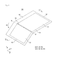
- a display panel 100 includes a substrate including a first region D1, a second region D2, and a third region D3.
- each of the first region D1 and the second region D2 may be a region in which an image is displayed.
- a first display portion may be located in the first region D1 and a second display portion may be located in the second region D2.
- the first region D1 and the second region D2 may each include a plurality of display elements which are turned on sequentially to represent (e.g., display) brightness corresponding to the data voltage applied thereto.
- the first region D1 may be a main display screen of a display region D
- the second region D2 may be an auxiliary display screen of the display region D, but are not limited thereto.
- the first region D1 and the second region D2 may display one image as a whole, but are not limited thereto.
- the first region D1 and the second region D2 may display different images.
- the third region D3 may be formed between the first region D1 and the second region D2.
- the third region D3 may extend in a first direction X to couple (e.g., connect) one end of the first region D1 to one end of the second region D2.
- the second region D2 may be positioned to continue the first region D1 through the third region D3.
- the second region D2, the third region D3, and the first region D1 may be arranged sequentially along a second direction Y that crosses (e.g., is perpendicular to) the first direction X.
- the substrate of the display panel 100 may be in a folded state.
- the directions of displayed images may be different from each other. That is, the second region D2 may be folded to be orientated in a different direction than the first region D1.
- the first region D1 and the second region D2 may be folded with respect to the third region D3.
- the second region D2 may be in a bent state along a bending line B-B' that is formed at one side of the third region D3.
- the second region D2 may be folded in a direction different from an orientation direction of the first region D1.
- the second region D2 may be folded with respect to the first region D1.
- the bending direction of the second region D2 may be a counterclockwise direction R1 as shown in FIG. 2 , but it is not limited thereto.
- the bending direction of the second region D2 may be a clockwise direction R2 (e.g., opposite to the counterclockwise direction R1).
- the second region D2 may be bent in an upward direction with respect to the first region D1.
- the third region D3 may be a region connecting the first region D1 and the second region D2 which display images in different directions.
- the first region D1 and the second region D2 may be substantially planar. Accordingly, the second region D2 that is bent to an extent in the counterclockwise direction R1 may form an internal angle ⁇ 1 with the first region D1.
- the internal angle ⁇ 1 between the first region D1 and the second region D2 may be reversely proportional to a distance d1 of an external curved surface of the third region D3. That is, as the internal angle ⁇ 1 becomes smaller, the distance d1 of the external curved surface may increase.
- the distance d1 of the external curved surface may be a cross-sectional region of the third region D3 and may be a region in which the drive portion, to be further described later, is mounted.
- the distance d1 of the external curved surface of the third region D3 and the internal angle ⁇ 1 may be preset in consideration of bending stresses of the first region D1 and the second region D2.
- the display panel 100 includes the second region D2 that extends from the first region D1 that is the main display region, and thus, a wider image or various images can be provided to a user.
- the substrate of the display panel 100 may include a flexible material.
- the substrate at the third region D3 may include a flexible material. That is, with respect to the third region D3, the first region D1 and the second region D2 may be transformed into a state opposite to the currently folded state (e.g., a flat state).
- the substrate of the display panel 100 may be formed of a flexible material. That is, all of the first region D1, the second region D2, and the third region D3 may be flexible.
- the third region D3 may be a region that is bent more frequently than the first region D1 and the second region D2 and may be formed of a more flexible material than that of the first region D1 and the second region D2.
- the third region D3 may correspond to a bent portion of the flexible display panel and may be an invisible region that is not recognized by (e.g., visible to) a user's eye E.
- the third region D3 may correspond to a boundary region (e.g., a boundary surface) between the first region D1 and the second region D2 which is in a bent state and, thus, may not be easily recognized by the user's eye E. Accordingly, even when one image is displayed on both the first region D1 and the second region D2 or different images are respectively displayed on the first region D1 and the second region D2, deterioration of the display quality that is caused by the third region D3 can be reduced or minimized.
- the first region D1, the second region D2, and the third region D3 may be defined as one display region D.
- the display panel 100 may further include a non-display region N formed at an edge portion of the display region D and surrounding the display region D.
- the non-display region N may be at an outer region of the first region D1 and the second region D2.
- a drive circuit for driving the first region D1 and the second region D2 may be mounted.
- the third region D3 may also include a drive portion that drives the first region D1 and the second region D2.
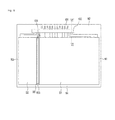
- FIG. 6 is a block diagram of a display panel according to an embodiment of the present invention, and shows the respective components of the display panel 100 in a state before bending (e.g., in a flat state).
- the non-display region N may be formed at an outer portion of the display region D to surround the display region D.
- the non-display region N may be divided into first to fourth non-display regions N1 to N4 according to the direction in which the display region D is arranged.
- various kinds of circuits and wirings for supplying an image signal to display elements positioned in the display region D may be arranged, and the display elements of the display region D may display the provided image signal.
- the display panel 100 may include a pad portion 101, a driver IC 102, and a scan drive portion 103.
- the pad portion 101 may be formed on the second non-display region N2.
- the pad portion 101 may be a region in which a flexible printed circuit board (FPCB) transmitting an external signal is coupled (e.g., connected).
- the pad portion 101 may transmit the external signal to the driver IC 102.
- FPCB flexible printed circuit board
- the driver IC 102 may be formed on the second non-display region N2.
- the formation positions of the driver IC 102 and the pad portion 101 in FIG. 6 are merely exemplary, and the present invention is not limited thereto.
- the driver IC 102 may generate a data voltage in response to the provided external signal and provide the data voltage to the first display portion of the first region D1 and the second display portion of the second region D2.
- the scan drive portion 103 may provide the scan signal to the first region D1 and the second region D2 in response to the scan control signal.
- the display elements of the first region D1 and the second region D2 may be turned on by the scan signal to receive the data voltage that is provided from the driver IC 102.
- the scan drive portion 103 is not formed on the non-display region N but may be formed on the third region D3 that corresponds to the bent region of the display region D.
- the scan drive portion 103 is formed on the third region D3 that is the bent region of the display region D, and thus, a relatively narrow non-display region N can be formed. By implementing the relatively narrow bezel, an extended display screen can be provided.
- the third region D3 of the display panel may include not only the scan drive portion 103 but also a power supply portion for supplying power to each pixel or a light emitting control portion when each pixel includes an organic light emitting element.
- the non-display region N becomes narrower, and the display panel can provide a narrower bezel.
- the scan drive portion 103 is arranged between the first region D1 and the second region D2, the transmission distance of the scan signal is shortened, and thus, attenuation of the scan signal can be reduced or prevented.
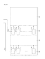
- FIG. 7 is a block diagram of a scan drive portion and a display region according to an embodiment of the present invention.
- the respective stages s1 to sn may correspond to the respective scan lines of the first region D1 and the second region D2 to provide the scan signals to the corresponding scan lines.
- the scan signals may be output through the buffers b1 to bn coupled to the respective stages s1 to sn.
- the scan signals may be successively generated through the first to n-th stages s1 to sn and may be successively provided to the respective scan lines.
- the first stage s1 may provide the first scan signal to the first buffer b1 and the second stage s2 in response to the scan control signal SL.
- the second stage s2 may generate a second scan signal in response to the first scan signal and may provide the generated second scan signal to the second buffer b2 and the third stage s3.
- the respective stages s1 to sn may provide the generated scan signals to the next stages, and the next stages may form the scan signals in response to the provided scan signals. Further, a gate-on voltage and a gate-off voltage may be provided to the respective stages s1 to sn, and the scan signal of the next stage may be fed back to the previous stage to control the scan signal output of the previous stage.
- the plurality of buffers b1 to bn may amplify the scan signals provided from the plurality of stages s1 to sn coupled thereto and may output the amplified scan signals to a first node.
- the scan signals provided to the first node may be transmitted to the first transistor Tr1 and the second transistor Tr2.
- the first transistor Tr1 and the second transistor Tr2 may be respectively turned on in response to a first scan selection signal En1 and a second scan selection signal En2 and, thus, may transmit the transmitted scan signals to the scan lines coupled thereto.
- the first region D1 and the second region D2 may include a plurality of display elements PX that are arranged in the form of a matrix.
- the display elements PX may be pixels of various display devices, such as an organic light emitting device, a liquid crystal display, and an electrophoretic display. In this embodiment, the display elements PX are described as organic light emitting elements, but the display elements are not limited thereto.
- the plurality of display elements PX in the first region D1 may be turned on in response to the first to n-th scan signals S11 to S1 n and, thus, may receive data voltages D11 to D1 m that are provided from the driver IC 102.
- the plurality of display elements PX in the second region D2 may be turned on in response to the first to n-th scan signals S21 to S2n and, thus, may receive data voltages D21 to D2j that are provided from the driver IC 102.
- the scan signal control portion 104 may receive the scan selection signal En from the scan drive terminal portion 101 a and may generate the first scan selection signal En1 and the second scan selection signal En2 in response to the scan selection signal En. For example, the scan signal control portion 104 may provide at least one of the first scan selection signal En1 and the second scan selection signal En2 to the scan drive portion 103.
- the scan signal control portion 104 may be formed on the second non-display region N2 as illustrated in FIG. 7 but is not limited thereto.
- the scan signal control portion 104 may be formed on the third region D3 of the display region D.
- the scan signal control portion 104 may output the first scan selection signal En1 only in response to the scan selection signal En to turn on the first transistor Tr1 only. Further, when only the second region D2 is to display an image, the scan signal control portion 104 may output the second scan selection signal En2 only in response to the scan selection signal En to turn on the second transistor Tr2 only. Further, when both the first region D1 and the second region D2 are to display images, the scan signal control portion 104 may output both the first scan selection signal En1 and the second scan selection signal En2 to turn on both the first transistor Tr1 and the second transistor Tr2.
- the scan drive portion 103 of the display panel 100 can selectively provide the scan signals to the first region D1 and/or the second region D2 and, thus, power consumption can be reduced.
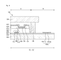
- FIG. 8 is a cross-sectional view of a display panel taken along the line VI-VI' of FIG. 6 .
- FIG. 8 is a cross-sectional view schematically illustrating the first region D1 and a portion of the second non-display region N2. The structure of the first region D1 to be further described below may also be applied to the second region D2.
- the first substrate 106 may include a polymer having high heat resistance.
- the first substrate 106 may include polyethersulfone (PES), polyarylate (PAR), polyetherimide (PEI), polyethylene naphthalate (PEN), polyethylene terephthalate (PEN), polyphenylene sulfide (PPS), polyacrylate, polyimide (PI), polycarbonate (PC), cellulose triacetate, cellulose acetate propionate (CAP), poly(arylene ether sulfone), and/or a combination thereof.
- the first substrate 106 may be flexible. That is, the first substrate 106 may be a substrate which can change shape, such as by rolling, folding, and/or bending.
- the first substrate 106 may include a display region D and a non-display region N.
- the display region D may be a region on which an image is displayed. Further, the display region D may be a region on which display elements for displaying an image and thin film transistors electrically coupled to (e.g., electrically connected to) the display elements are positioned. The display elements may be organic light emitting elements but are not limited thereto.
- the non-display region N may be a region on which no image is displayed. Further, the non-display region N may be a region on which the sealant 136 and the terminal portion 101 c are positioned. Further, the non-display region N may be a region that is adjacent to an edge of the first substrate 106. For example, the non-display region N may be a region that is positioned at an edge portion of the first substrate 106.
- the non-display region N may surround the display region D.
- the non-display region N may have a circular donut shape that surrounds the entire display region D.
- the semiconductor pattern 108 may be formed on the first substrate 106.
- the semiconductor pattern 108 may be positioned on the display region D of the first substrate 106.
- the semiconductor pattern 108 may be formed on the buffer layer.
- the semiconductor pattern 108 may be made of amorphous semiconductor, microcrystalline semiconductor, or polycrystalline semiconductor.
- the semiconductor pattern 108 is made of polycrystalline semiconductor.
- the semiconductor pattern 108 may also be made of oxide semiconductor.
- the semiconductor pattern 108 may include a channel portion that is not doped with an impurity and a source portion and a drain portion that are each doped with p+ on respective sides of the channel portion.
- a doped ion material may be a P-type impurity, such as boron (B), and, for example, B 2 H 6 .
- the impurity may differ depending on the kind of thin film transistor.
- the gate insulating layer 110 may be formed to cover the semiconductor pattern 108 on the buffer layer.
- the gate insulating layer 110 may be positioned on the display region D and the non-display region N of the first substrate 106.
- the gate insulating layer 110 may be made of silicon oxide (SiO x ), silicon nitride (SiN x ), or metal oxide.
- the gate electrode 112 may be formed on the gate insulating layer 110.
- the gate electrode 112 may be positioned on the display region D of the first substrate 106.
- the gate electrode 112 may be formed on a portion of the gate insulating layer 110 below which the semiconductor pattern 108 is positioned.
- the gate electrode 112 may include metal, an alloy, metal nitride, conductive metal oxide, or a transparent conductive material. Further, the gate electrode 112 and the channel portion may overlap each other. However, the dimensions of the gate electrode 112 and/or the dimensions of the channel portion may be varied depending on the electrical characteristics of the switching element including the same.
- the interlayer insulating layer 114 may be formed on the gate insulating layer 110 to cover the gate electrode 112 and the pad terminal 101-1c.
- the interlayer insulating layer 114 may be formed on the display region D and on the non-display region N of the first substrate 106.
- the interlayer insulating layer 114 may be formed on the gate insulating layer 110 along profiles of the gate electrode 112 and the pad terminal 101-1c to have a substantially uniform thickness. Accordingly, a step height portion that is adjacent to the gate electrode 112 and the pad terminal 101-1c may be formed in (e.g., under) the interlayer insulating layer 114.
- the interlayer insulating layer 114 may be made of silicon compound.
- the interlayer insulating layer 114 may serve to insulate the gate electrode 112 from a source electrode 116 and a drain electrode 118 to be subsequently formed.
- the interlayer insulating layer 114 may include a first contact opening (e.g., a first contact hole) for exposing a part of the semiconductor pattern 108 and a second contact opening (e.g., a second contact hole) for exposing a part of the pad terminal 101-1c.
- the first contact opening may be formed on the display region D of the first substrate 106.
- the first contact opening may expose a source portion and a drain portion of the semiconductor pattern 108.
- the first contact opening may be formed to penetrate the gate insulating layer 110.
- the first contact opening may be formed to extend in a direction that is perpendicular to a surface of the first substrate 106.
- the second contact opening may be formed on the non-display region N of the first substrate 106.
- the second contact opening may expose a center portion of the pad terminal 101-1c.
- the second contact opening may be formed to extend in the direction that is perpendicular to the surface of the first substrate 106.
- the source electrode 116 and the drain electrode 118 may be formed on the interlayer insulating layer 114.
- the source electrode 116 and the drain electrode 118 may be inserted into the first contact opening.
- the source electrode 116 and the drain electrode 118 may be formed on the display region D of the first substrate 106.
- the source electrode 116 and the drain electrode 118 may be arranged to be spaced from (e.g., spaced apart from) each other by a distance (e.g., a predetermined distance) around the gate electrode 112 and to be adjacent to the gate electrode 112.
- the source electrode 116 and the drain electrode 118 may penetrate the interlayer insulating layer 114 and the gate insulating layer 110 and may come in contact with the source portion and the drain portion of the semiconductor pattern 108.
- the source electrode 116 and the drain electrode 118 may include metal, an alloy, metal nitride, conductive metal oxide, or a transparent conductive material.
- a thin film transistor which includes the semiconductor pattern 108, the gate insulating layer 110, the gate electrode 116, and the drain electrode 118, may be provided on the first substrate 106 as a switching element of the organic light emitting display device.
- the thin film transistor may be a top-gate thin film transistor.
- the auxiliary terminal 101-2c may also be formed on the interlayer insulating layer 114.
- the auxiliary terminal 101-2c may be inserted into the second contact opening. That is, the auxiliary terminal 101-2c may be formed on the non-display region N of the first substrate 106.
- One pad terminal 101-1c and one auxiliary terminal 101-2c may constitute one terminal portion 101c.
- the driver IC 102 may be mounted on the terminal portion 101c.
- the intermediate layer 120 may be formed on the source electrode 116 and the drain electrode 118.
- the intermediate layer 120 may be formed on the interlayer insulating layer 114 to cover the source electrode 116 and the drain electrode 118.
- the intermediate layer 120 may be formed on the display region D of the first substrate 106.
- the intermediate layer 120 may have a thickness that is sufficient to completely cover the source electrode 116 and the drain electrode 118.
- the intermediate layer 120 may be include an organic material or an inorganic material.
- the planarization layer 122 may be formed on the intermediate layer 120.
- the planarization layer 122 may be formed on the display region D of the first substrate 106.
- the surface of the planarization layer 122 may be flat.
- the planarization layer 122 may be formed having a sufficient thickness to planarize one surface on which a pixel is positioned.
- the planarization layer 122 may be made of an insulating material.
- the planarization layer 122 may include a via-hole (e.g., a via-opening) that exposes a portion of the drain electrode 118.
- the via-hole may expose the center portion of the drain electrode 118.
- the via-hole may be formed to extend in the direction that is perpendicular to the surface of the substrate 106.
- the first electrode 124 may be positioned on the planarization layer 122.
- the first electrode 124 may be formed on the display region D of the first substrate 106.
- the first electrode 124 may be in the via-hole and may be electrically coupled to the drain electrode 118.
- the first electrode 124 may be an anode electrode or a cathode electrode.
- the second electrode 130 is a cathode electrode.
- the first electrode 124 maybe a cathode electrode
- the second electrode 130 may be an anode electrode.
- the first electrode 124 When the first electrode 124 is the anode electrode, the first electrode 124 may be made of a conductive material having a high work function. When the display device is a bottom emission type display device, the first electrode 124 may be formed of a material, such as ITO, IZO, ZnO, or In 2 O 3 or a laminate thereof. When the display device is a top emission type display device, the first electrode 124 may further include a reflection layer that is formed of, for example, Ag, Mg, Al, Pt, Pd, Au, Ni, Nd, Ir, Cr, Li, or Ca. The first electrode 124 may be variously modified, such as by being at least a two-layer structure using at least two different materials as described above.
- the pixel defining layer 126 may be formed on the first electrode 124.
- the pixel defining layer 126 may be formed on the display region D of the first substrate 106.
- the pixel defining layer 126 may expose some regions (e.g., portions) of the first electrode 124.
- the pixel defining layer 126 may include at least one organic material, such as benzocyclobutene (BCB), polyimide (PI), polyamide (PA), acryl resin, and/or phenol resin, or may include an inorganic material, such as silicon nitride.
- the pixel defining layer 126 may also be made of a photoconductor including a black pigment, and in this embodiment, the pixel defining layer 126 may act as a light shield member.
- the organic light emitting layer 128 may be formed on the first electrode 124.
- the organic light emitting layer 128 may be formed on the display region D of the first substrate 106.
- current is applied to the organic light emitting layer 128, electrons and holes are recombined in the organic light emitting layer 128 to form excitations and light having a specific wavelength is generated by energy from the formed excitations.
- the organic light emitting layer 128 may be made of a low molecular weight organic material or a high molecular weight organic material.
- the organic light emitting layer 128 may include a hole-injection layer (HIL), a hole-transporting layer (HTL), a hole blocking layer (HBL), a light emitting layer (EML), an electron-transporting layer (ETL), an electron-injection layer (EIL), and/or an electron blocking layer (EBL).
- HIL hole-injection layer
- HTL hole-transporting layer
- HBL hole blocking layer
- EML electron-transporting layer
- EIL electron-injection layer
- EBL electron blocking layer
- the second electrode 130 may be formed on the organic light emitting layer 128.
- the second electrode 130 may be formed on the display region D of the first substrate 106.
- the second electrode 130 may be made of a conductive material having a low work function.
- the second electrode 130 may be formed of Ag, Mg, Al, Pt, Pd, Au, Ni, Nd, Ir, Cr, Li, or Ca.
- an organic light emitting element which includes the first electrode 124, the organic light emitting layer 128, and the second electrode 130, may be provided on the first substrate 106 as a display element of the display device.
- the protection layer 132 may be formed on the second electrode 130.
- the protection layer 132 may be formed on the display region D of the first substrate 106.
- the protection layer 132 may prevent or reduce deterioration of the display element by protecting the display element from external moisture or oxygen.
- the protection layer 132 may be an organic layer, an inorganic layer, or have a multilayer structure including these layers.
- the protection layer 132 may be formed using an evaporation method, a CVD method, or a sputtering method.
- the second substrate 134 may be positioned on the protection layer 132.
- the second substrate 134 may be spaced from (e.g., spaced apart from) the protection layer 132 by a distance (e.g., by a predetermined distance). Nitrogen may fill between the second substrate 134 and the protection layer 132. The second substrate 134 may face the first substrate 106. The second substrate 134 may be positioned to cover the whole display region D and a part (e.g., a portion) of the non-display region N of the first substrate 106. The second substrate 134 may encapsulate the display elements and thin film transistors together with the sealant 136.
- the second substrate 134 may be made of transparent plastic but is not limited thereto.
- the second substrate 134 may be made of various materials that can intercept external materials (e.g., prevent external materials from passing therethrough).
- the second substrate 134 may be made of the same material as that of the first substrate 106.
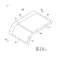
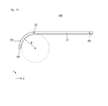
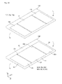
- FIG. 9 is a perspective view schematically illustrating a display panel according to another embodiment of the present invention
- FIG. 10 is a cross-sectional view of a display panel taken along the line VIII-VIII' of FIG. 9 .
- a display panel 200 includes a display region D and a non-display region N.
- the display region D may include a first region D1, a second region D2, and a third region D3.
- the first region D1 and the second region D2 may be regions on which an image is displayed.
- the second region D2 may be positioned to extend from one end of the first region D1 to continue the first region D1.
- the first region D1 may be a main display screen of the display region D, and the second region D2 may be an auxiliary display screen of the display region D, but the regions are not limited thereto.
- the third region D3 may be formed between the first region D1 and the second region D2.
- the first region D1 of the display panel 200 may have a substantially planar shape, and the second region D2 may have a curved surface shape that is bent along a curvature (e.g., a preset curvature). As illustrated in FIG. 10 , the second region D2 may be bent in a counterclockwise direction R1 so as to have a radius of curvature R.
- the second region D2 may be a part of a circumference of a circle having a constant radius of curvature R. In one embodiment, a length of the second region D2 may be about 1/4 of the circumference of the circle or less but is not limited thereto.
- the display panel 200 including the same can provide an improved sense of grip and sense of beauty.
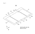
- FIG. 11 is a perspective view schematically illustrating a display panel according to still another embodiment of the present invention.
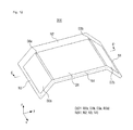
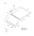
- FIG. 12 is a perspective view illustrating a display panel that is bent along the line B-B' of FIG. 11
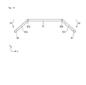
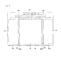
- FIG. 13 is a cross-sectional view of a display panel taken along the line C-C' of FIG. 12 .
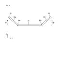
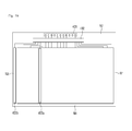
- FIG. 14 is a cross-sectional view of a display panel that is bent in the opposite direction of the direction in FIG. 13 .
- a display panel 300 includes a display region D and a non-display region N.
- the display region D may include a first region D1, second regions D2a and D2b, and third regions D3a and D3b.
- the first region D1 and the second regions D2a and D2b may be regions on which an image is displayed.
- the first region D1 may be a main display screen of the display region D
- the second regions D2a and D2b may be auxiliary display screens of the display region D but are not limited thereto.
- the third regions D3a and D3b may be formed on both sides of the first region D1.
- the third regions D3a and D3b may be formed between the first region D1 and the second regions D2a and D2b, respectively.
- the third region D3a may extend in a first direction X to couple one end of the first region D1 to an end of the second region D2b arranged on one side thereof
- the third region D3b may extend in the first direction X to couple the other end of the first region D1 to an end of the second region D2b arranged on the other side thereof.
- the second region D2a arranged on one side of the first region D1 may be positioned to continue the first region D1 through the third region D3a, and the second region D2b arranged on the other side of the first region D1 may be positioned to continue the first region D1 through the third region D3b.
- the display region D may be arranged in the order of the second region D2a, the third region D3a, the first region D1, the third region D3b, and the second region D2b along a second direction Y that crosses (e.g., is perpendicular to) the first direction X.
- the third regions D3a and D3b may be bent regions.
- the first region D1 and the second regions D2a and D2b of the display region D may be bent along the third region D3a and D3b.
- the second regions D2a and D2b may be bent along the bending lines B-B'.
- the second region D2a that is arranged on one side of the first region D1 may be bent in a counterclockwise direction R1 along the bending line formed on one side of the third region D3a
- the second region D2b that is arranged on the other side of the first region D1 may be bent in a clockwise direction R2 along the bending line formed on the other side of the third region D3b.
- the second regions D2a and D2b may be bent to face each other along the third regions D3a and D3b.
- the second regions D2a and D2b may be bent in an upward direction with respect to the first region D1.
- the display panel 300 may be a display panel in which the left and right sides of the display region D are bent to provide an extended display screen.
- the second regions D2a and D2b are formed on the left and right sides of the first region D1, respectively, but are not limited thereto.
- the second regions D2a and D2b may be formed on upper and lower sides of the first region D1 or at other positions.
- the display panel 300 may be in a fixed state after being bent, but it is not limited thereto.
- the third region D3 may include a flexible material and may be transformed into a state opposite to the currently folded state or a flat state.
- the entire substrate of the display panel 300 may be formed of a flexible material.
- all of the first region D1, the second regions D2a and D2b, and the third regions D3a and D3b may be flexible.
- the third region D3 may be a region that is bent more frequently than the first region D1 and the second region D2 and may be formed of a more flexible material than that of the first region D1 and the second regions D2a and D2b.
- the third regions D3a and D3b correspond to bent portions of the flexible display panel and may be invisible regions that are not recognized by a user's eye.
- the third regions D3a and D3b may correspond to boundary surfaces (e.g., interfaces) between the first region D1 and the second regions D2a and D2b, respectively, which are in a bent state and, thus, may not be easily recognized by the user's eye. Accordingly, even if one image is displayed on both the first region D1 and the second regions D2a and D2b or different images are respectively displayed on the first region D1 and the second regions D2a and D2b, deterioration of the display quality that is caused by the third regions D3a and D3b can be reduce or minimized.
- the third regions D3a and D3b may include a drive portion that drives the first region D1 and the second regions D2a and D2b, respectively. Hereinafter, this will be described in more detail with reference to FIGS. 12 and 13 .
- FIG. 15 is a block diagram of a display panel according to still another embodiment of the present invention
- FIG. 16 is a block diagram of a scan drive portion and a display region according to still another embodiment of the present invention.
- the third region D3a may include a first scan drive portion 303a
- the third region D3b may include a second scan drive portion 303b.
- the first scan drive portion 303a may provide the scan signal to the second region D2a arranged on one side of the first region D1 and to the first region D1
- the second scan drive portion 303b may provide the scan signal to the second region D2b arranged on the other side of the first region D1.
- the scan drive portion 303a may include a plurality of stages s1 to sn successively generating the scan signals, a plurality of buffers b1 to bn coupled to terminals of the plurality of stages s1 to sn to amplify the generated scan signals, and a first transistor Tr1 and a second transistor Tr2 coupled to terminals of the plurality of buffers b1 to bn.
- the scan drive portion 303b may include a plurality of stages s1 to sn successively generating the scan signals and a third transistor Tr3 coupled to the terminals of the plurality of stages s1 to sn. Because the second scan drive portion 303b provides the scan signal only to the second region D2a arranged on the other side, the buffers can be omitted.
- the first to third transistors Tr1 to Tr3 may be respectively turned on in response to first to third scan selection signals En1 to En3 and, thus, may transmit the transmitted scan signals to the scan lines coupled thereto.
- the first scan drive portion 303a and the second scan drive portion 303b may selectively provide the scan signals to the first region D1 and the second region D2 according to the first to third scan selection signals En1 to En3.
- the first to third scan selection signals En1 to En3 may be generated by a scan signal control portion 340.
- the scan signal control portion 340 may generate the first to third scan selection signals En1 to En3 in response to the scan selection signal En and may provide at least one of the first to third scan selection signals En1 to En3 to the first region D1 or the second region D2.
- FIG. 17 is a perspective view schematically illustrating a display panel according to still another embodiment of the present invention
- FIG. 18 is a perspective view illustrating a display panel that is bent along the line B-B' of FIG. 17 .
- a display panel 400 includes a display region D and a non-display region N.
- the display region D may include a first region D1, a second region D2, and a third region D3.
- the first region D1 and the second region D2 may be regions on which an image is displayed.
- the first region D1 may be a main display screen of the display region D
- the second region D2 may be an auxiliary display screen of the display region D but are not limited thereto.
- the third region D3 may be formed between the first region D1 and the second region D2.
- the third region D3 may extend in a first direction X to couple one end of the first region D1 to the other end of the second region D2.
- the second region D2 may be positioned to continue the first region D1 through the third region D3.
- the display region D may be arranged in the order of the second region D2, the third region D3, and the first region D1 along a second direction Y that crosses (e.g., is perpendicular to) the first direction X.
- the third region D3 may be a bent region.
- the first region D1 and the second region D2 of the display region D may be bent along the third region D3.
- the second region D2 may be bent along the bending line B-B' that is formed on one side of the third region D3.
- the third region D3 corresponds to a bent portion of the flexible display panel and may be an invisible region that is not recognized by a user's eye.
- the third region D3 may correspond to a boundary surface (e.g., an interface) between the first region D1 and the second region D2 which is in a bent state and, thus, may not be easily recognized by the user's eye.
- the third region D3 may include a first drive portion 403a that drives the first region D1
- the non-display region N may include a second drive portion 403b that drives the second region D2.
- FIG. 19 is a block diagram of a display panel according to still another embodiment of the present invention
- FIG. 20 is a block diagram of a scan drive portion and a display region according to still another embodiment of the present invention.
- the display panel 400 may further include a driver IC 402 and a pad portion 401.
- the driver IC 402 may be formed on the first non-display region N1 in the non-display region N and may provide data voltages to the first region D1 and the second region D2.
- the pad portion 401 may be formed on the second non-display region N2, and may provide a data control signal, a first scan control signal SL1, and a second scan control signal SL2 to the driver IC 402, the first scan drive portion 403a, and the second scan drive portion 403b, respectively.
- the formation positions of the driver IC 402 and the pad portion 401 are not limited to those as described above.
- the driver IC 402 may be formed on the third region D3, and thus, a relatively narrow non-display region can be formed.
- the first scan drive portion 403a and the second scan drive portion 403b may each include a plurality of stages s1 to sn.
- the plurality of stages s1 to sn of the first scan drive portion 403a may be coupled to the scan lines of the first region D1 to provide the scan signals.
- the plurality of stages s1 to sn of the second scan drive portion 403b may be coupled to the scan lines of the second region D2 and may provide the scan signals.
- the scan signals may be successively generated from the first stage s1 to the n-th stage sn and may be successively provided to the scan lines.
- the respective stages s1 to sn may provide the generated scan signals to the next stage, and the next stage may generate the scan signal in response to the scan signals of the previous stage.
- the first stage s1 of the first scan drive portion 403a and the first stage s1 of the second drive portion 403b may output the scan signals in response to the first scan control signal SL1 and the second scan control signal SL2.
- the driving of the first scan drive portion 403a and the second scan drive portion 403b may be controlled by the first scan control signal SL1 and the second scan control signal SL2, respectively.
- the pad portion 401 may output and provide at least one of the first scan control signal SL1 and the second scan control signal SL2 to the first scan drive portion 403a and the second scan drive portion 403b.
- the pad portion 401 may output the first scan control signal SL1 and/or the second scan control signal SL2.
- the pad portion 401 can output only the first scan control signal SL1
- the pad portion 401 can output only the second scan control signal SL2.
- the pad portion 401 may provide both the first scan control signal SL1 and the second scan control signal SL2.
- the pad portion 401 of the display panel can provide a signal that can selectively drive the first region D1 and the second region D2, the power consumption can be reduced. Further, because the drive circuit mounted on the third region D3 has a simpler configuration than the drive circuit of the display panel 100 as described above, the area of the third region D3 that is a region between the first region D1 and the second region D2 can be further reduced.
- FIG. 21 is an exploded cross-sectional view of a display device according to an embodiment of the present invention
- FIG. 22 is a cross-sectional view of a display device according to an embodiment of the present invention
- FIG. 23 is a schematic view illustrating a relationship between a display panel and a touch panel.
- the display device 10 includes a display panel 100', a touch panel 140, a transparent protection window 150, and a housing 160.
- the display panel 100' has substantially the same or the same configuration as that of the display panel 300 described above, the detailed description thereof may be omitted.
- the display panel 100' is not limited the configuration described above and may be the same or substantially the same as the display panel according to any other embodiment described above.
- the touch panel 140 may be arranged on the display panel 100'.
- the touch panel 140 may be one of various suitable touch types, such as a capacitance type or a resistance type.
- the touch panel 140 may be a flexible touch panel that include a flexible material and may be formed of a transparent material because it is arranged on an upper portion of the display panel 100' on which an image is displayed.
- the display panel 100' may include a display region D and a non-display region N that is at an outer portion of the display region D.
- the touch panel 140 may include a touch region T and a wiring region that is at an outer portion of the touch region T.
- the touch region T may include a first touch region T1 and second touch regions T2a and T2b.
- the display region D of the display panel 100' may correspond to the touch region T of the touch panel 140, and the non-display region N of the display panel 100' may correspond to the wiring region of the touch panel 140.
- the first region D1 and the first touch region T1 may be aligned to correspond to each other
- the second regions D2a and D2b and the second touch regions T2a and T2b may be aligned to respectively correspond to each other
- the touch panel 140 and the display panel 100' my be joined to each other.
- Sides of the display panel 100' that is combined with the touch panel 140 may be bent along the third regions D3a and D3b.
- the touch panel 140 may have a gap space, which corresponds to the third regions D3a and D3b of the display panel 100', between the first touch region T1 and the second touch region T2, and the touch panel 140 may be easily bent at the gap space.
- the display panel 100' may be fixed to the touch panel 140 by the transparent protection window 150 and the housing 160.
- the transparent protection window 150 may be joined to an upper surface of the display panel 100' on which an image is displayed to correspond to a bent shape of the display panel 100'. That is, the transparent protection window 150 may be arranged on the touch panel 140.
- the display panel 100' may correspond to the shape of the touch panel 140, and one end and the other end of the transparent protection window 150 may be joined to one end and the other end of the housing 160, respectively.
- the transparent protection window 150 may be transparent such that the display screen of the display panel 100' is easily visible to a user through the transparent protection window 150. Further, the transparent protection window 150 may protect the display panel 100' from an external impact and scratch and may function as a support to maintain the bent shape of the display panel 100'.
- An adhesive layer for adhesion may be formed between the touch panel 140 and the display panel 100' and between the touch panel 140 and the transparent protection window 150.
- the housing 160 may include a support portion 161 and a seat portion 162.
- the support portion 161 may be a space in which the display panel 100' is arranged.
- the support portion 161 may be configured to support the display panel 100' and to maintain the curved surface shape of the display panel 100'.
- the seat portion 162 may be a space in which end portions of the display panel 100' and the touch panel 140 are fixed. Further, the seat portion 162 may prevent the non-display region N of the display panel 100' and the wiring region of the touch panel from being visually recognized to an outside.
- One end and the other end of the housing 160 may be formed to project in an upward direction and may be combined with one end and the other end of the transparent protection window 150 as described above.
- the drive portion is formed in the third region D3, and thus, the non-display region is reduced to provide an extended image screen. Further, because the respective display regions can be individually driven, the power consumption can be reduced.
Landscapes
- Engineering & Computer Science (AREA)
- Physics & Mathematics (AREA)
- General Physics & Mathematics (AREA)
- Theoretical Computer Science (AREA)
- Computer Hardware Design (AREA)
- Chemical & Material Sciences (AREA)
- Crystallography & Structural Chemistry (AREA)
- Devices For Indicating Variable Information By Combining Individual Elements (AREA)
- Manufacturing & Machinery (AREA)
- Microelectronics & Electronic Packaging (AREA)
- Electroluminescent Light Sources (AREA)
Applications Claiming Priority (2)
| Application Number | Priority Date | Filing Date | Title |
|---|---|---|---|
| KR20140039399 | 2014-04-02 | ||
| KR1020140194760A KR102315687B1 (ko) | 2014-04-02 | 2014-12-31 | 표시 패널 및 이를 포함하는 표시 장치 |
Publications (2)
| Publication Number | Publication Date |
|---|---|
| EP2927901A2 true EP2927901A2 (fr) | 2015-10-07 |
| EP2927901A3 EP2927901A3 (fr) | 2015-10-21 |
Family
ID=52814842
Family Applications (1)
| Application Number | Title | Priority Date | Filing Date |
|---|---|---|---|
| EP15162271.9A Withdrawn EP2927901A3 (fr) | 2014-04-02 | 2015-04-01 | Panneau d'affichage |
Country Status (3)
| Country | Link |
|---|---|
| US (1) | US10255863B2 (fr) |
| EP (1) | EP2927901A3 (fr) |
| CN (1) | CN104978899B (fr) |
Cited By (3)
| Publication number | Priority date | Publication date | Assignee | Title |
|---|---|---|---|---|
| EP3246914A3 (fr) * | 2016-05-19 | 2018-01-17 | Samsung Display Co., Ltd. | Dispositif d'affichage |
| EP3373280A4 (fr) * | 2015-11-13 | 2018-12-05 | Samsung Electronics Co., Ltd. | Procédé de commande d'affichage, panneau d'affichage le mettant en oeuvre, dispositif d'affichage et dispositif électronique |
| EP3493187A4 (fr) * | 2016-07-29 | 2020-01-01 | Boe Technology Group Co. Ltd. | Circuit de pilotage, panneau d'affichage, dispositif d'affichage et procédé de pilotage |
Families Citing this family (32)
| Publication number | Priority date | Publication date | Assignee | Title |
|---|---|---|---|---|
| KR102379745B1 (ko) * | 2015-07-06 | 2022-03-29 | 삼성디스플레이 주식회사 | 표시 장치 |
| KR102455045B1 (ko) * | 2015-09-18 | 2022-10-18 | 삼성디스플레이 주식회사 | 표시장치 |
| KR102403205B1 (ko) | 2015-10-21 | 2022-05-30 | 엘지디스플레이 주식회사 | 디스플레이 패널 및 디스플레이 디바이스 |
| KR102409906B1 (ko) * | 2015-10-22 | 2022-06-17 | 삼성디스플레이 주식회사 | 플렉서블 표시 장치 |
| KR102544695B1 (ko) * | 2015-12-14 | 2023-06-16 | 삼성디스플레이 주식회사 | 표시 장치 |
| CN105374315B (zh) * | 2015-12-28 | 2019-01-04 | 昆山工研院新型平板显示技术中心有限公司 | 一种柔性显示装置及其驱动方法 |
| CN106935614B (zh) * | 2015-12-30 | 2019-12-31 | 南京瀚宇彩欣科技有限责任公司 | 环状显示装置与其制造方法 |
| CN105513501B (zh) * | 2016-02-29 | 2018-07-24 | 天马微电子股份有限公司 | 一种柔性显示面板以及显示装置 |
| TWI792916B (zh) * | 2016-06-24 | 2023-02-11 | 日商半導體能源研究所股份有限公司 | 顯示裝置、電子裝置 |
| CN105977280B (zh) * | 2016-07-21 | 2019-01-11 | 北京小米移动软件有限公司 | 显示装置的制作方法和显示装置 |
| KR102348595B1 (ko) * | 2016-10-26 | 2022-01-07 | 주식회사 토비스 | 일부 휘어진 곡면부를 갖는 대형 디스플레이장치 |
| KR102600695B1 (ko) * | 2016-12-23 | 2023-11-09 | 엘지디스플레이 주식회사 | 표시장치 |
| US10664014B2 (en) * | 2017-01-05 | 2020-05-26 | Wuhan China Star Optoelectronics Technology Co., Ltd | Flexible display panel and flexible display apparatus |
| CN115425052A (zh) * | 2017-06-29 | 2022-12-02 | 京东方科技集团股份有限公司 | 显示面板及显示装置 |
| KR20190010052A (ko) * | 2017-07-20 | 2019-01-30 | 엘지전자 주식회사 | 디스플레이 디바이스 |
| CN109389953A (zh) * | 2017-08-08 | 2019-02-26 | 京东方科技集团股份有限公司 | 扫描驱动电路及其驱动方法、显示装置 |
| KR102524340B1 (ko) * | 2018-02-22 | 2023-04-25 | 삼성디스플레이 주식회사 | 플렉서블 표시 장치 및 이의 제조 방법 |
| KR102060033B1 (ko) * | 2018-03-29 | 2019-12-27 | (주)코텍 | 디스플레이장치 |
| KR102533660B1 (ko) * | 2018-07-04 | 2023-05-17 | 삼성디스플레이 주식회사 | 표시 장치 |
| KR102662203B1 (ko) * | 2018-07-17 | 2024-04-30 | 삼성디스플레이 주식회사 | 플렉시블 표시 장치 |
| CN108877535B (zh) * | 2018-07-27 | 2020-08-28 | 武汉天马微电子有限公司 | 可折叠显示面板及显示装置 |
| KR102649236B1 (ko) * | 2019-04-04 | 2024-03-21 | 삼성디스플레이 주식회사 | 표시 장치 |
| CN111833806A (zh) * | 2019-04-19 | 2020-10-27 | 北京小米移动软件有限公司 | 显示屏组件、显示控制方法、装置及终端 |
| KR102673772B1 (ko) * | 2019-07-29 | 2024-06-12 | 삼성디스플레이 주식회사 | 영상 보정부를 포함하는 표시장치 |
| CN112447138A (zh) * | 2019-09-05 | 2021-03-05 | 北京小米移动软件有限公司 | 显示屏幕的驱动方法及装置 |
| CN110675751B (zh) * | 2019-09-24 | 2022-02-08 | Oppo广东移动通信有限公司 | 显示装置及终端设备 |
| CN110707143B (zh) * | 2019-11-13 | 2022-03-04 | 京东方科技集团股份有限公司 | 显示面板、制备方法及显示装置 |
| CN110850627A (zh) * | 2019-11-29 | 2020-02-28 | 厦门天马微电子有限公司 | 一种显示面板及显示装置 |
| CN114489364B (zh) * | 2020-11-11 | 2025-03-28 | 京东方科技集团股份有限公司 | 显示装置及其控制方法 |
| KR102826935B1 (ko) * | 2020-11-13 | 2025-07-01 | 삼성디스플레이 주식회사 | 표시장치 |
| TWI912643B (zh) * | 2023-09-26 | 2026-01-21 | 群創光電股份有限公司 | 電子裝置 |
| CN118553163A (zh) * | 2024-06-07 | 2024-08-27 | 昆山国显光电有限公司 | 一种显示面板及显示装置 |
Family Cites Families (24)
| Publication number | Priority date | Publication date | Assignee | Title |
|---|---|---|---|---|
| US6688528B2 (en) * | 1997-07-15 | 2004-02-10 | Silverbrook Research Pty Ltd | Compact display assembly |
| KR101041057B1 (ko) * | 2004-01-09 | 2011-06-13 | 삼성전자주식회사 | 표시장치 |
| KR100551486B1 (ko) * | 2004-10-21 | 2006-02-13 | 삼성전자주식회사 | 비동작 디스플레이에 대한 간섭을 방지하는 디스플레이제어 회로를 구비한 다중 디스플레이 장치 및 이를 위한다중 디스플레이 제어 방법 |
| KR101074417B1 (ko) * | 2005-06-14 | 2011-10-18 | 엘지디스플레이 주식회사 | 쉬프트 레지스터와 이를 이용한 액정표시장치 |
| KR101293567B1 (ko) * | 2006-02-21 | 2013-08-06 | 삼성디스플레이 주식회사 | 표시장치의 제조방법 |
| US8564543B2 (en) * | 2006-09-11 | 2013-10-22 | Apple Inc. | Media player with imaged based browsing |
| CN101290409B (zh) * | 2007-04-17 | 2010-05-19 | 北京京东方光电科技有限公司 | 栅极驱动电路及液晶显示器 |
| US8497821B2 (en) * | 2009-02-16 | 2013-07-30 | Global Oled Technology Llc | Chiplet display device with serial control |
| US9070323B2 (en) | 2009-02-17 | 2015-06-30 | Global Oled Technology Llc | Chiplet display with multiple passive-matrix controllers |
| KR20110061423A (ko) | 2009-12-01 | 2011-06-09 | 엘지디스플레이 주식회사 | 듀얼 표시장치 |
| TWM391664U (en) * | 2010-05-28 | 2010-11-01 | Qiao-Yu Tong | Application device of E-paper software |
| US8194399B2 (en) * | 2010-07-16 | 2012-06-05 | Hewlett-Packard Development Company, L.P. | Altering the flexibility of a display device |
| KR101700701B1 (ko) * | 2010-09-24 | 2017-02-14 | 삼성전자 주식회사 | 화상 표시 장치 |
| KR101862347B1 (ko) * | 2011-02-01 | 2018-07-05 | 삼성디스플레이 주식회사 | 표시장치 및 이를 갖는 표시장치 세트 |
| JP2012237868A (ja) | 2011-05-11 | 2012-12-06 | Kyocera Display Corp | 液晶表示装置 |
| KR101320384B1 (ko) | 2011-06-30 | 2013-10-23 | 삼성디스플레이 주식회사 | 가요성 표시 패널 및 상기 가요성 표시 패널을 포함하는 표시 장치 |
| JP5687965B2 (ja) * | 2011-07-05 | 2015-03-25 | 株式会社フジクラ | 光コネクタ、コネクタ接続ユニット |
| KR101843199B1 (ko) | 2011-12-15 | 2018-03-29 | 엘지디스플레이 주식회사 | 플렉서블 유기발광다이오드 표시장치 및 그 제조 방법 |
| US8896202B2 (en) * | 2012-02-28 | 2014-11-25 | Lg Electronics Inc. | Display device |
| CN103514840B (zh) * | 2012-06-14 | 2016-12-21 | 瀚宇彩晶股份有限公司 | 集成门极驱动电路及液晶面板 |
| KR101910111B1 (ko) * | 2012-08-28 | 2018-10-22 | 삼성디스플레이 주식회사 | 접이식 표시 장치 |
| CN104956429B (zh) * | 2013-01-30 | 2017-10-03 | 夏普株式会社 | 显示装置 |
| KR102105959B1 (ko) * | 2013-07-22 | 2020-04-29 | 엘지전자 주식회사 | 이미지 레이어를 제공하는 폴더블 디스플레이 디바이스 및 그 제어 방법 |
| KR102039496B1 (ko) * | 2013-08-19 | 2019-11-04 | 삼성디스플레이 주식회사 | 접이식 표시 장치 |
-
2015
- 2015-03-13 US US14/658,116 patent/US10255863B2/en active Active
- 2015-03-30 CN CN201510145603.5A patent/CN104978899B/zh active Active
- 2015-04-01 EP EP15162271.9A patent/EP2927901A3/fr not_active Withdrawn
Non-Patent Citations (1)
| Title |
|---|
| None |
Cited By (8)
| Publication number | Priority date | Publication date | Assignee | Title |
|---|---|---|---|---|
| EP3373280A4 (fr) * | 2015-11-13 | 2018-12-05 | Samsung Electronics Co., Ltd. | Procédé de commande d'affichage, panneau d'affichage le mettant en oeuvre, dispositif d'affichage et dispositif électronique |
| US10629132B2 (en) | 2015-11-13 | 2020-04-21 | Samsung Electronics Co., Ltd. | Display device and electronic device including a plurality of separately driven display areas and display control method for controlling the same |
| US11017725B2 (en) | 2015-11-13 | 2021-05-25 | Samsung Electronics Co., Ltd. | Display device and electronic device including a plurality of separately driven display areas and display control method for controlling the same |
| EP3246914A3 (fr) * | 2016-05-19 | 2018-01-17 | Samsung Display Co., Ltd. | Dispositif d'affichage |
| US10388228B2 (en) | 2016-05-19 | 2019-08-20 | Samsung Display Co., Ltd. | Display device |
| US10978003B2 (en) | 2016-05-19 | 2021-04-13 | Samsung Display Co., Ltd. | Display device with concave area |
| EP3493187A4 (fr) * | 2016-07-29 | 2020-01-01 | Boe Technology Group Co. Ltd. | Circuit de pilotage, panneau d'affichage, dispositif d'affichage et procédé de pilotage |
| US10692441B2 (en) | 2016-07-29 | 2020-06-23 | Boe Technology Group Co., Ltd. | Drive circuit and drive method for foldable display panel and display device |
Also Published As
| Publication number | Publication date |
|---|---|
| CN104978899B (zh) | 2019-11-01 |
| US20150287365A1 (en) | 2015-10-08 |
| EP2927901A3 (fr) | 2015-10-21 |
| CN104978899A (zh) | 2015-10-14 |
| US10255863B2 (en) | 2019-04-09 |
Similar Documents
| Publication | Publication Date | Title |
|---|---|---|
| US10255863B2 (en) | Display panel having a first region, a second region, and a third region between the first and second regions and including a drive portion on the third region | |
| US11690265B2 (en) | Display device having a trench portion | |
| KR102845810B1 (ko) | 표시 장치 | |
| KR102315687B1 (ko) | 표시 패널 및 이를 포함하는 표시 장치 | |
| US11690281B2 (en) | Display apparatus | |
| KR20200015868A (ko) | 표시 패널 | |
| EP3633751A1 (fr) | Dispositif d'affichage | |
| KR20210027718A (ko) | 표시 장치 | |
| US20230397467A1 (en) | Display apparatus including overlapping elements | |
| KR20200128286A (ko) | 접을 수 있는 표시 장치 | |
| CN115955864A (zh) | 显示设备 | |
| KR20150002290A (ko) | 박막 트랜지스터 어레이 기판 및 이를 포함하는 유기발광표시장치 | |
| CN221596455U (zh) | 显示装置 | |
| EP4280848A1 (fr) | Appareil d'affichage | |
| US20240040863A1 (en) | Display apparatus | |
| US20240324349A1 (en) | Display apparatus | |
| US12615915B2 (en) | Display device including shift area, main display area and extended display area | |
| US20250212604A1 (en) | Display apparatus and method of manufacturing the same | |
| US20260013369A1 (en) | Display apparatus, method of manufacturing display apparatus, and electronic apparatus including display apparatus | |
| US20250241152A1 (en) | Display apparatus | |
| CN116156943A (zh) | 显示装置 | |
| CN118695675A (zh) | 显示装置 | |
| KR20210031583A (ko) | 디스플레이 장치 |
Legal Events
| Date | Code | Title | Description |
|---|---|---|---|
| PUAL | Search report despatched |
Free format text: ORIGINAL CODE: 0009013 |
|
| PUAI | Public reference made under article 153(3) epc to a published international application that has entered the european phase |
Free format text: ORIGINAL CODE: 0009012 |
|
| AK | Designated contracting states |
Kind code of ref document: A2 Designated state(s): AL AT BE BG CH CY CZ DE DK EE ES FI FR GB GR HR HU IE IS IT LI LT LU LV MC MK MT NL NO PL PT RO RS SE SI SK SM TR |
|
| AX | Request for extension of the european patent |
Extension state: BA ME |
|
| AK | Designated contracting states |
Kind code of ref document: A3 Designated state(s): AL AT BE BG CH CY CZ DE DK EE ES FI FR GB GR HR HU IE IS IT LI LT LU LV MC MK MT NL NO PL PT RO RS SE SI SK SM TR |
|
| AX | Request for extension of the european patent |
Extension state: BA ME |
|
| RIC1 | Information provided on ipc code assigned before grant |
Ipc: G09G 3/20 20060101AFI20150916BHEP Ipc: G09G 3/32 20060101ALI20150916BHEP |
|
| 17P | Request for examination filed |
Effective date: 20160118 |
|
| RBV | Designated contracting states (corrected) |
Designated state(s): AL AT BE BG CH CY CZ DE DK EE ES FI FR GB GR HR HU IE IS IT LI LT LU LV MC MK MT NL NO PL PT RO RS SE SI SK SM TR |
|
| 17Q | First examination report despatched |
Effective date: 20170529 |
|
| STAA | Information on the status of an ep patent application or granted ep patent |
Free format text: STATUS: THE APPLICATION IS DEEMED TO BE WITHDRAWN |
|
| 18D | Application deemed to be withdrawn |
Effective date: 20191130 |