EP2928061A1 - Stromwandlersystem und verfahren zur steuerung davon - Google Patents
Stromwandlersystem und verfahren zur steuerung davon Download PDFInfo
- Publication number
- EP2928061A1 EP2928061A1 EP13858200.2A EP13858200A EP2928061A1 EP 2928061 A1 EP2928061 A1 EP 2928061A1 EP 13858200 A EP13858200 A EP 13858200A EP 2928061 A1 EP2928061 A1 EP 2928061A1
- Authority
- EP
- European Patent Office
- Prior art keywords
- inverter
- lower arm
- arm portion
- semiconductor switches
- terminals
- Prior art date
- Legal status (The legal status is an assumption and is not a legal conclusion. Google has not performed a legal analysis and makes no representation as to the accuracy of the status listed.)
- Granted
Links
Images


Classifications
-
- H—ELECTRICITY
- H02—GENERATION; CONVERSION OR DISTRIBUTION OF ELECTRIC POWER
- H02M—APPARATUS FOR CONVERSION BETWEEN AC AND AC, BETWEEN AC AND DC, OR BETWEEN DC AND DC, AND FOR USE WITH MAINS OR SIMILAR POWER SUPPLY SYSTEMS; CONVERSION OF DC OR AC INPUT POWER INTO SURGE OUTPUT POWER; CONTROL OR REGULATION THEREOF
- H02M3/00—Conversion of DC power input into DC power output
- H02M3/02—Conversion of DC power input into DC power output without intermediate conversion into AC
- H02M3/04—Conversion of DC power input into DC power output without intermediate conversion into AC by static converters
- H02M3/10—Conversion of DC power input into DC power output without intermediate conversion into AC by static converters using discharge tubes with control electrode or semiconductor devices with control electrode
- H02M3/145—Conversion of DC power input into DC power output without intermediate conversion into AC by static converters using discharge tubes with control electrode or semiconductor devices with control electrode using devices of a triode or transistor type requiring continuous application of a control signal
- H02M3/155—Conversion of DC power input into DC power output without intermediate conversion into AC by static converters using discharge tubes with control electrode or semiconductor devices with control electrode using devices of a triode or transistor type requiring continuous application of a control signal using semiconductor devices only
- H02M3/156—Conversion of DC power input into DC power output without intermediate conversion into AC by static converters using discharge tubes with control electrode or semiconductor devices with control electrode using devices of a triode or transistor type requiring continuous application of a control signal using semiconductor devices only with automatic control of output voltage or current, e.g. switching regulators
- H02M3/158—Conversion of DC power input into DC power output without intermediate conversion into AC by static converters using discharge tubes with control electrode or semiconductor devices with control electrode using devices of a triode or transistor type requiring continuous application of a control signal using semiconductor devices only with automatic control of output voltage or current, e.g. switching regulators including plural semiconductor devices as final control devices for a single load
- H02M3/1582—Buck-boost converters
-
- H—ELECTRICITY
- H02—GENERATION; CONVERSION OR DISTRIBUTION OF ELECTRIC POWER
- H02P—CONTROL OR REGULATION OF ELECTRIC MOTORS, ELECTRIC GENERATORS OR DYNAMO-ELECTRIC CONVERTERS; CONTROLLING TRANSFORMERS, REACTORS OR CHOKE COILS
- H02P6/00—Arrangements for controlling synchronous motors or other dynamo-electric motors using electronic commutation dependent on the rotor position; Electronic commutators therefor
- H02P6/14—Electronic commutators
-
- H—ELECTRICITY
- H02—GENERATION; CONVERSION OR DISTRIBUTION OF ELECTRIC POWER
- H02M—APPARATUS FOR CONVERSION BETWEEN AC AND AC, BETWEEN AC AND DC, OR BETWEEN DC AND DC, AND FOR USE WITH MAINS OR SIMILAR POWER SUPPLY SYSTEMS; CONVERSION OF DC OR AC INPUT POWER INTO SURGE OUTPUT POWER; CONTROL OR REGULATION THEREOF
- H02M7/00—Conversion of AC power input into DC power output; Conversion of DC power input into AC power output
- H02M7/42—Conversion of DC power input into AC power output without possibility of reversal
- H02M7/44—Conversion of DC power input into AC power output without possibility of reversal by static converters
- H02M7/48—Conversion of DC power input into AC power output without possibility of reversal by static converters using discharge tubes with control electrode or semiconductor devices with control electrode
- H02M7/53—Conversion of DC power input into AC power output without possibility of reversal by static converters using discharge tubes with control electrode or semiconductor devices with control electrode using devices of a triode or transistor type requiring continuous application of a control signal
- H02M7/537—Conversion of DC power input into AC power output without possibility of reversal by static converters using discharge tubes with control electrode or semiconductor devices with control electrode using devices of a triode or transistor type requiring continuous application of a control signal using semiconductor devices only, e.g. single switched pulse inverters
- H02M7/5387—Conversion of DC power input into AC power output without possibility of reversal by static converters using discharge tubes with control electrode or semiconductor devices with control electrode using devices of a triode or transistor type requiring continuous application of a control signal using semiconductor devices only, e.g. single switched pulse inverters in a bridge configuration
-
- H—ELECTRICITY
- H02—GENERATION; CONVERSION OR DISTRIBUTION OF ELECTRIC POWER
- H02M—APPARATUS FOR CONVERSION BETWEEN AC AND AC, BETWEEN AC AND DC, OR BETWEEN DC AND DC, AND FOR USE WITH MAINS OR SIMILAR POWER SUPPLY SYSTEMS; CONVERSION OF DC OR AC INPUT POWER INTO SURGE OUTPUT POWER; CONTROL OR REGULATION THEREOF
- H02M1/00—Details of apparatus for conversion
- H02M1/0067—Converter structures employing plural converter units, other than for parallel operation of the units on a single load
Definitions
- the present invention relates to a power conversion system for driving a load, such as an alternating current motor, and to a control method of the power conversion system.
- 10 is a direct current power source
- 20 is a current reversible boost converter (DC/DC converter)
- 21 and 22 are semiconductor switches
- 23 is a reactor
- 30 is a capacitor
- 40 is a three-phase voltage inverter
- 41 to 46 are semiconductor switches
- 50 is an alternating current motor.
- each of the semiconductor switches 21, 22, and 41 to 46 is configured of a semiconductor switching element, such as an IGBT, and a reflux diode connected in reverse parallel thereto.
- the voltage of the capacitor 30 is boosted with respect to the voltage of the direct current power source 10.
- the inverter 40 by turning on and off the semiconductor switches 41 to 46 by, for example, PWM control, converts the direct current voltage of the capacitor 30 to a three-phase alternating current voltage and supplies the three-phase alternating current voltage to the alternating current motor 50.
- a direct current power source 10 is connected between a neutral point (the neutral point of a stator winding) 50a of an alternating current motor 50 and a negative side direct current busbar, and the same numbers as in Fig. 4 are given to other components.
- a zero-phase equivalent circuit formed of the direct current power source 10
- a leakage inductance (a zero-phase inductance) of the alternating current motor 50, and the inverter 40 comes to have substantially the same circuit configuration as the boost converter 20 in Fig. 4 , and it is thus possible to control the voltage of the capacitor 30 to a higher value than the voltage of the direct current power source 10.
- a drive operation of the alternating current motor 50 by the inverter 40 is the same as in Fig. 4 .
- Fig. 6 is a circuit diagram showing the heretofore known technology described in PTL 3.
- 70 is a DC/DC converter which operates as a buck-boost chopper
- 71 to 74 are semiconductor switches
- 75 is a reactor, wherein the series circuit of the semiconductor switches 71 and 72 is connected in parallel to a direct current power source 10 and capacitor 31, and the series circuit of the semiconductor switches 73 and 74 is connected in parallel to a capacitor 32 and inverter 40.
- 11 and 62 are voltage detectors
- 61 is a current detector
- 80 is a control circuit.
- the duty ratio of the semiconductor switches 71 and 74 to 72 and 73 of the DC/DC converter 70 is controlled, thereby changing energy stored in the reactor 75, and the voltage of the direct current power source 10 is controlled to a desired size and output to the capacitor 32 side.
- NPL 1 Comparative Evaluation of Soft-Switching Concepts for Bi-directional Buck+Boost Dc-Dc Converters, p. 1856-1865, The 2010 International Power Electronics Conference ( Fig. 1 )
- the heretofore known technology of Fig. 5 has a problem that as the inverter 40 is caused to operate as a zero-phase converter by appropriately switching the inverter 40 in the operation of switching the inverter 40 which drives the alternating current motor 50, a boost operation is constantly carried out while the alternating current motor 50 is operating, due to which the loss in the inverter 40 and alternating current motor 50 increases.
- a problem to be solved by the invention is to provide a power conversion system wherein by eliminating the need for a boost reactor and constant boost operation, it is possible to achieve a reduction in the size of the whole system and a loss reduction, and to enhance the degree of freedom of the direct current voltage of an inverter, and a control method of the power conversion system.
- a power conversion system includes a power storage device such as a capacitor; an inverter, between the positive and negative direct current terminals of which the power storage device is connected, and between a plurality of alternating current terminals of which a load having an inductance is connected; a first upper and lower arm portion, configured by connecting first and second semiconductor switches in series, of which the connection point of the first and second semiconductor switches is connected to the neutral point of the load; and a direct current power source such as a battery connected in parallel to the first upper and lower arm portion, wherein at least one pair of homopolar terminals, of pairs of homopolar terminals out of the positive and negative direct current terminals of the inverter and the positive and negative terminals of the first upper and lower arm portion, are connected by a switch, and the other pair of homopolar terminals are set at the same potential.
- a power storage device such as a capacitor
- an inverter between the positive and negative direct current terminals of which the power storage device is connected, and between a plurality of alternating current terminals of which
- pairs of homopolar terminals, of the positive and negative direct current terminals of the inverter and the positive and negative terminals of the first upper and lower arm portion are connected one pair by each switch, and that one switch is constantly placed in an on state, and the other switch is brought into an on and off operation.
- semiconductor switches configuring the inverter and the first and second semiconductor switches configuring the first upper and lower arm portion are each configured of a semiconductor switching element and a reflux diode connected in reverse parallel thereto.
- the switch in claim 2 is turned off, and all the semiconductor switches in the upper arm or lower arm of the inverter are turned on or off at the same time, thereby equivalently configuring a second upper and lower arm portion formed of the series circuit of third and fourth semiconductor switches, and that the first and second semiconductor switches are turned on and off, thereby causing a buck-boost chopper formed of the first upper and lower arm portion, the second upper and lower arm portion, and the inductance of the load to operate, thus charging and discharging the capacitor.
- the need for a boost reactor is eliminated by utilizing an inductance which a load such as an alternating current motor has, it is possible to reduce the size and price of the whole system. Also, as it is possible to select an operation mode in which the load is driven by an inverter without using a boost operation, a simplification in control is achieved, and a loss reduction is possible, compared with a heretofore known technology wherein a boost operation is constantly carried out.
- the load is, for example, an alternating current motor
- the direct current voltage of the inverter when the load is, for example, an alternating current motor, raise the direct current voltage of the inverter when the motor rotates at high speed, meaning that it is possible to reduce current with the motor set to be of high voltage specifications, and thus achieve a reduction in the diameter of a cable through which to supply power to the motor, a reduction in the size of connection terminals, and the like.
- Fig. 1 is a circuit diagram showing an embodiment of the invention.
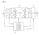
- the positive and negative direct current terminals of a three-phase voltage inverter 40 formed of semiconductor switches 41 to 46 are connected one to each end of a capacitor 30 acting as a power storage device, and a three-phase alternating current motor 50 is connected to the alternating current terminals of the inverter 40.
- an upper and lower arm portion 90 wherein semiconductor switches 91 and 92 are connected in series are connected between the positive pole and negative pole of a direct current power source 10 formed of a battery or the like, and the connection point of the semiconductor switches 91 and 92 is connected to a neutral point 50a of the alternating current motor 50.
- the semiconductor switches 91 and 92 are called first and second semiconductor switches, and the upper and lower arm portion 90 is called a first upper and lower arm portion.
- the positive terminal of the upper and lower arm portion 90 (the positive pole of the direct current power source 10) is connected to one direct current terminal (positive terminal) of the inverter 40 via a switch 100 formed of a bidirectional semiconductor switch or a mechanical switch, while the negative terminal of the upper and lower arm portion 90 (the negative pole of the direct current power source 10) is directly connected to the other direct current terminal (negative terminal) of the inverter 40, and both negative terminals are kept at the same potential.
- a configuration may be such that the switch 100 is connected between the negative terminal of the upper and lower arm portion 90 and the negative terminal of the inverter 40, and that the positive terminal of the upper and lower arm portion 90 and the positive terminal of the inverter 40 are directly connected together and kept at the same potential.
- switches may be connected, one between the positive terminal of the upper and lower arm portion 90 and the positive terminal of the inverter, and the other between the negative terminal of the upper and lower arm portion 90 and the negative terminal of the inverter.
- a configuration only has to be such that while a power conversion system is operating, one switch (which corresponds to the switch 100 of the embodiment) is turned on or off by an operation, to be described hereafter, while the other switch is constantly placed in an on state, and both ends of the other switch are kept at the same potential, and that when the power conversion system stops, the other switch is turned off.
- the semiconductor switches 41 to 46, 91, and 92 are each configured of a semiconductor switching element, such as an IGBT, and a reflux diode connected in reverse parallel thereto, as illustrated in the brackets in Fig. 1 .
- the direct current power source 10 and the capacitor 30 are connected in parallel to the direct current circuit of the inverter 40, thus configuring an alternating current motor drive system, formed of a common three-phase voltage inverter, as the whole circuit.
- the inverter 40 by carrying out PWM control or the like in accordance with a predetermined voltage command given from a control circuit (not shown) and thus turning on and off the semiconductor switches 41 to 46, converts a direct current voltage to a three-phase alternating current voltage and supplies the three-phase alternating voltage to the alternating current motor 50.
- 40A is an upper and lower arm portion which equivalently shows the inverter 40 acting as a zero-phase converter
- an upper-arm semiconductor switch 47 corresponds to the semiconductor switches 41, 43, and 45 in Fig. 1 which are turned on or off at the same time
- a lower-arm semiconductor switch 48 corresponds to the semiconductor switches 42, 44, and 46 in Fig. 1 which are turned off or on at the same time.
- the semiconductor switches 47 and 48 configuring the upper and lower arm portion 40A are called third and fourth semiconductor switches
- the upper and lower arm portion 40A is called a second upper and lower arm portion.
- connection point of the semiconductor switches 47 and 48 in Fig. 2 is connected to the connection point of the semiconductor switches 91 and 92 of the upper and lower arm portion 90 via a leakage inductance (a zero-phase inductance) 51 of the alternating current motor 50, and a buck-boost converter 70A is configured of the upper and lower arm portions 40A and 90 and the leakage inductance 51.
- the circuit shown in Fig. 2 is substantially the same in overall configuration as the previously described circuit in Fig. 6 , and the buck-boost converter 70A in Fig. 2 has the same function as circuits described in, for example, Fig. 3 in Japanese Patent No. 3, 666, 557 and Figs. 1 and 2 in Japanese Patent No. 5,029,315 .
- the zero-phase voltage of the inverter 40 is controlled in accordance with the zero-phase voltage command, and zero-phase power is exchanged between the direct current power source 10 and the capacitor 30 by the switching operations of the upper and lower arm portion 40A acting as an equivalently configured zero-phase converter and of the other upper and lower arm portion 90, thus enabling a buck-boost operation to be carried out.
- the semiconductor switches 42, 44, and 46 in the lower arm of the inverter 40 in Fig. 1 are turned on at the same time (the semiconductor switch 48 in Fig. 2 is turned on), and the semiconductor switch 91 of the upper and lower arm portion 90 is turned on, by the zero-phase voltage command, energy is stored in the leakage inductance 51 from the direct current power source 10.
- the semiconductor switches 42, 44, and 46 in the lower arm of the inverter 40 in Fig. 1 are turned off at the same time (the semiconductor switch 48 in Fig. 2 is turned off) and the semiconductor switch 91 is turned off, the energy stored in the leakage inductance 51 is supplied to the capacitor 30 via the reflux diodes of the semiconductor switches 41, 43, and 45 (the semiconductor switch 47 in Fig. 2 ) and the reflux diode of the semiconductor switch 92, meaning that it is possible to charge the capacitor 30.
- the semiconductor switch 91 may be maintained in an on state.
- the buck-boost capacitor 70A in Fig. 2 is such that the semiconductor switches 47 and 48 of the upper and lower arm portion 40A and the semiconductor switches 91 and 92 of the upper and lower arm portion 90 in Figs. 1 and 2 are turned on and off, thereby causing current to flow from the direct current power source 10 to the leakage inductance 51 in Fig. 2 and thus storing energy in the leakage inductance 51, and furthermore, the energy is supplied to the capacitor 30 via the reflux diodes of the semiconductor switches 47 and 92 in Fig. 2 , meaning that it is possible to charge the capacitor 30 using the energy of the direct current power source 10.
- the semiconductor switches 91 and 92 of the upper and lower arm portion 90 and the leakage inductance 51 operate as a buck chopper
- the semiconductor switches 47 and 48 of the upper and lower arm portion 40A and the leakage inductance 51 operate as a boost chopper. Therefore, by adjusting the duty ratio of the semiconductor switches 91, 92, 47, and 48 configuring the buck and boost choppers, it is possible to control the direct current voltage of the inverter 40 (the voltage of the capacitor 30), and thus the alternating current output voltage of the inverter 40, with respect to the voltage of the direct current power source 10 at a high degree of freedom.
- the buck-boost converter 70A is caused to operate as a buck-boost chopper, as previously described, the degree of freedom of the direct current voltage of the inverter 40 is high, and it is thus possible to output a desired size of alternating current voltage to drive the alternating current motor 50.
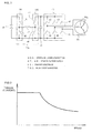
- a permanent magnet synchronous motor used in, for example, an electric vehicle or a hybrid car in general, having the kinds of speed-torque characteristics shown in Fig. 3 , is such that the current of the motor is substantially proportional to the torque, it may be conceivable that the speed-current characteristics of the motor are also substantially the same as in Fig. 4 .
- the embodiment is suitable for a kind of case in which a boost operation is carried out in a high speed region which does not require so much torque.
- the terminal voltage of the alternating current motor in general, rises along with an increase in rotation speed, in the event that it is possible to carry out a boost operation, it is possible, in accordance therewith, to design the terminal voltage of the motor to be a high voltage. As a result of this, current flowing through the motor is suppressed, thus enabling a contribution to a reduction in the diameter of a cable through which to supply power to the motor, a reduction in the size of connection terminals and semiconductor elements, and a reduction in the size, weight, and cost of the whole system owing to the reduced volume.
- the invention can be utilized in each kind of drive system wherein a load is driven by an inverter, including an in-vehicle power conversion system mounted on, for example, an electric vehicle or hybrid car.
Landscapes
- Engineering & Computer Science (AREA)
- Power Engineering (AREA)
- Inverter Devices (AREA)
- Control Of Ac Motors In General (AREA)
Applications Claiming Priority (2)
| Application Number | Priority Date | Filing Date | Title |
|---|---|---|---|
| JP2012259641 | 2012-11-28 | ||
| PCT/JP2013/078907 WO2014083980A1 (ja) | 2012-11-28 | 2013-10-25 | 電力変換システム及びその制御方法 |
Publications (3)
| Publication Number | Publication Date |
|---|---|
| EP2928061A1 true EP2928061A1 (de) | 2015-10-07 |
| EP2928061A4 EP2928061A4 (de) | 2017-03-08 |
| EP2928061B1 EP2928061B1 (de) | 2018-01-10 |
Family
ID=50827626
Family Applications (1)
| Application Number | Title | Priority Date | Filing Date |
|---|---|---|---|
| EP13858200.2A Not-in-force EP2928061B1 (de) | 2012-11-28 | 2013-10-25 | Stromwandlersystem und verfahren zur steuerung davon |
Country Status (5)
| Country | Link |
|---|---|
| US (1) | US9843278B2 (de) |
| EP (1) | EP2928061B1 (de) |
| JP (1) | JP5858309B2 (de) |
| CN (1) | CN104737435B (de) |
| WO (1) | WO2014083980A1 (de) |
Families Citing this family (14)
| Publication number | Priority date | Publication date | Assignee | Title |
|---|---|---|---|---|
| JP5452782B1 (ja) * | 2013-04-09 | 2014-03-26 | 三菱電機株式会社 | 駆動装置 |
| FR3056037B1 (fr) * | 2016-09-14 | 2018-08-17 | Valeo Equipements Electriques Moteur | Systeme de transfert de puissance electrique |
| US10250059B2 (en) * | 2016-09-19 | 2019-04-02 | Microsoft Technology Licensing, Llc | Charging circuit for battery-powered device |
| KR101936992B1 (ko) * | 2016-10-26 | 2019-01-10 | 현대자동차주식회사 | 권선형 동기 전동기를 이용한 충전 시스템 |
| KR101966501B1 (ko) * | 2016-10-26 | 2019-08-14 | 현대자동차주식회사 | 권선형 동기 전동기를 이용한 충전 시스템 |
| CN108347167B (zh) * | 2017-01-25 | 2021-07-13 | 通用电气公司 | 用于软切换dc—dc转换器的系统和方法 |
| DE102018120236A1 (de) * | 2018-08-20 | 2020-02-20 | Thyssenkrupp Ag | Ladevorrichtung mit steuerbarer Zwischenkreismittelpunktsspannung sowie Antriebssystem mit einer derartigen Ladevorrichtung |
| JP7160479B2 (ja) * | 2018-12-21 | 2022-10-25 | 株式会社デンソー | 電動機システム |
| JP7294982B2 (ja) * | 2019-10-18 | 2023-06-20 | 株式会社豊田中央研究所 | 電動機制御装置 |
| CN113119801B (zh) * | 2019-12-31 | 2023-12-12 | 比亚迪股份有限公司 | 车辆、能量转换装置及其控制方法 |
| CN113752909B (zh) * | 2020-06-04 | 2023-08-08 | 比亚迪股份有限公司 | 一种能量转换装置及车辆 |
| EP3988377B1 (de) * | 2020-10-23 | 2024-01-03 | Ningbo Geely Automobile Research & Development Co. Ltd. | Elektrisches fahrzeugsystem |
| JP7446390B2 (ja) * | 2021-11-08 | 2024-03-08 | 台達電子工業股▲ふん▼有限公司 | モータ駆動と電池の充放電を備えた電源統合システム |
| CN118232760A (zh) * | 2022-12-14 | 2024-06-21 | 采埃孚股份公司 | 电驱动系统、控制方法及相关设备 |
Family Cites Families (45)
| Publication number | Priority date | Publication date | Assignee | Title |
|---|---|---|---|---|
| FR2692734B1 (fr) * | 1992-06-23 | 1994-08-26 | Auxilec | Chaîne de traction électrique pour véhicule automobile. |
| US5397975A (en) * | 1993-06-14 | 1995-03-14 | Ecoair Corp. | Hybrid alternator |
| US5502368A (en) * | 1994-06-06 | 1996-03-26 | Ecoair Corp. | Hybrid alternator with voltage regulator |
| US5491622A (en) * | 1994-01-07 | 1996-02-13 | Delco Electronics Corp. | Power converter with emergency operating mode for three phase induction motors |
| JP3741171B2 (ja) * | 1996-06-17 | 2006-02-01 | 株式会社安川電機 | 多重パルス幅変調方式の電力変換装置 |
| DE19823917A1 (de) * | 1997-06-03 | 1998-12-10 | Fuji Electric Co Ltd | Stromrichtervorrichtung |
| JP3666557B2 (ja) | 1999-04-20 | 2005-06-29 | 富士電機機器制御株式会社 | 電力変換回路 |
| US6291963B2 (en) * | 1999-12-15 | 2001-09-18 | Nissan Motor Co., Ltd. | Drive circuit for motor/generator |
| JP3775468B2 (ja) * | 2000-01-19 | 2006-05-17 | 富士電機システムズ株式会社 | 交流電動機の可変速駆動システム |
| US6518736B2 (en) * | 2000-06-26 | 2003-02-11 | Toyota Jidosha Kabushiki Kaisha | Mechanical power outputting apparatus and inverter apparatus |
| JP3721116B2 (ja) | 2000-11-14 | 2005-11-30 | 株式会社豊田中央研究所 | 駆動装置,動力出力装置およびその制御方法 |
| JP4725694B2 (ja) * | 2001-02-01 | 2011-07-13 | 富士電機システムズ株式会社 | Pwm電力変換器の制御装置 |
| JP2003102181A (ja) * | 2001-09-25 | 2003-04-04 | Toyota Motor Corp | 電力供給システムおよび電力供給方法 |
| JP3692993B2 (ja) * | 2001-10-04 | 2005-09-07 | トヨタ自動車株式会社 | 駆動装置および動力出力装置 |
| JP4023171B2 (ja) * | 2002-02-05 | 2007-12-19 | トヨタ自動車株式会社 | 負荷駆動装置、負荷駆動装置における電力貯蔵装置の充電制御方法および充電制御をコンピュータに実行させるためのプログラムを記録したコンピュータ読取可能な記録媒体 |
| JP2004120844A (ja) | 2002-09-25 | 2004-04-15 | Fuji Electric Systems Co Ltd | 昇圧コンバータ制御装置 |
| JP4111059B2 (ja) | 2003-05-26 | 2008-07-02 | トヨタ自動車株式会社 | 電圧変換システム、電圧変換方法および制御プログラム |
| JP4063199B2 (ja) * | 2003-11-14 | 2008-03-19 | 日産自動車株式会社 | モータ駆動4wd車両の制御装置 |
| JP3993564B2 (ja) * | 2004-01-13 | 2007-10-17 | 三菱重工業株式会社 | シリーズハイブリッド電気自動車 |
| GB0415153D0 (en) * | 2004-07-06 | 2004-08-11 | Newage Int Ltd | Electrical machine rotor position identification |
| JP4517994B2 (ja) * | 2005-09-29 | 2010-08-04 | トヨタ自動車株式会社 | 充電制御装置および電動車両 |
| FR2892243B1 (fr) * | 2005-10-13 | 2008-01-18 | Airbus France Sas | Onduleur de tension reconfigurable a tolerence de pannes |
| JP2007220976A (ja) * | 2006-02-17 | 2007-08-30 | Toyota Motor Corp | 半導体モジュールおよびそれを備えるハイブリッド車両の駆動装置 |
| JP4747968B2 (ja) * | 2006-06-30 | 2011-08-17 | トヨタ自動車株式会社 | モータ駆動装置 |
| US7609050B2 (en) * | 2007-02-20 | 2009-10-27 | Gm Global Technology Operations, Inc. | Method and system for determing current in an electrical component in a power conversion system |
| EP1990908B1 (de) * | 2007-05-10 | 2010-03-31 | Denso Corporation | Elektrisches Drehsystem zur Verwendung einer Schaltung im Nullsystem |
| JP4483911B2 (ja) * | 2007-08-31 | 2010-06-16 | 株式会社デンソー | 車両用回転電機 |
| CN101801710B (zh) * | 2007-09-10 | 2012-07-18 | 丰田自动车株式会社 | 车辆的系统起动装置及车辆的系统起动方法 |
| JP4609474B2 (ja) * | 2007-10-10 | 2011-01-12 | 株式会社デンソー | 回転電機装置 |
| JP5040585B2 (ja) * | 2007-10-24 | 2012-10-03 | 富士電機株式会社 | 電力変換システム |
| JP4441920B2 (ja) * | 2007-11-22 | 2010-03-31 | 株式会社デンソー | 電源装置 |
| JP5029315B2 (ja) | 2007-11-22 | 2012-09-19 | 富士電機株式会社 | モータ駆動システム |
| JP5527497B2 (ja) * | 2008-01-11 | 2014-06-18 | 富士電機株式会社 | 交流電動機駆動回路及び電気車駆動回路 |
| JP4719776B2 (ja) * | 2008-07-14 | 2011-07-06 | トヨタ自動車株式会社 | 充電ケーブル、充電制御装置、及び車両充電システム |
| JP5251413B2 (ja) * | 2008-10-14 | 2013-07-31 | 株式会社デンソー | 同期電動機の駆動装置 |
| JP5412974B2 (ja) * | 2009-03-13 | 2014-02-12 | 株式会社デンソー | 三相交流同期電動機の駆動装置 |
| JP4800402B2 (ja) * | 2009-03-18 | 2011-10-26 | 株式会社豊田中央研究所 | 車両搭載用マルチフェーズコンバータ |
| US8063440B2 (en) * | 2009-05-28 | 2011-11-22 | GM Global Technology Operations LLC | Power electronics power module with imbedded gate circuitry |
| JP5493568B2 (ja) * | 2009-08-06 | 2014-05-14 | 株式会社デンソー | 電動機駆動装置及び電動機駆動装置の制御方法ならびに電動装置 |
| JP5434381B2 (ja) * | 2009-08-31 | 2014-03-05 | 株式会社デンソー | 車載電動機の駆動装置 |
| JP5686131B2 (ja) * | 2010-02-17 | 2015-03-18 | 富士電機株式会社 | 電力変換装置 |
| JP5104898B2 (ja) * | 2010-04-28 | 2012-12-19 | トヨタ自動車株式会社 | 電気システムの電力制限装置 |
| FR2961361B1 (fr) * | 2010-06-14 | 2013-07-12 | Hispano Suiza Sa | Onduleur de tension et procede de commande d'un tel onduleur |
| JP5365586B2 (ja) * | 2010-06-18 | 2013-12-11 | 富士電機株式会社 | 電力変換装置 |
| JP2012235659A (ja) * | 2011-05-09 | 2012-11-29 | Denso Corp | 回転機の制御装置 |
-
2013
- 2013-10-25 EP EP13858200.2A patent/EP2928061B1/de not_active Not-in-force
- 2013-10-25 CN CN201380055337.6A patent/CN104737435B/zh not_active Expired - Fee Related
- 2013-10-25 WO PCT/JP2013/078907 patent/WO2014083980A1/ja not_active Ceased
- 2013-10-25 JP JP2014550090A patent/JP5858309B2/ja not_active Expired - Fee Related
-
2015
- 2015-04-22 US US14/693,281 patent/US9843278B2/en not_active Expired - Fee Related
Non-Patent Citations (1)
| Title |
|---|
| See references of WO2014083980A1 * |
Also Published As
| Publication number | Publication date |
|---|---|
| US20150229252A1 (en) | 2015-08-13 |
| JP5858309B2 (ja) | 2016-02-10 |
| WO2014083980A1 (ja) | 2014-06-05 |
| CN104737435A (zh) | 2015-06-24 |
| US9843278B2 (en) | 2017-12-12 |
| JPWO2014083980A1 (ja) | 2017-01-05 |
| EP2928061B1 (de) | 2018-01-10 |
| EP2928061A4 (de) | 2017-03-08 |
| CN104737435B (zh) | 2018-05-29 |
Similar Documents
| Publication | Publication Date | Title |
|---|---|---|
| US9843278B2 (en) | Power conversion system and control method thereof | |
| US11431184B2 (en) | Power supply device | |
| US8508961B2 (en) | Power conversion apparatus | |
| US20130002186A1 (en) | Power converter | |
| KR101965558B1 (ko) | 제어 가능한 에너지 저장 장치에 하나 이상의 직류원을 연결하기 위한 연결 시스템 및 관련 작동 방법 | |
| US12580391B2 (en) | System for charging vehicle battery using motor driving system | |
| JP6439282B2 (ja) | 充電システム、給電車両、充電車両、及び充電方法 | |
| KR20230013551A (ko) | 모터 구동 시스템을 이용한 차량용 배터리 충전 시스템 | |
| JP5288178B2 (ja) | モータ駆動システム | |
| US20130249474A1 (en) | System for Charging an Energy Store, and Method for Operating the Charging System | |
| US9793850B2 (en) | Systems for charging an energy store, and method for operating the charging systems | |
| EP4108507A1 (de) | System zum laden einer fahrzeugbatterie mit einem motorantriebssystem | |
| US9457683B2 (en) | Method for discharging at least one capacitor of an electric circuit | |
| US9112359B2 (en) | System for charging an energy store, and method for operating the charging system | |
| US20140361619A1 (en) | Power device | |
| KR101036163B1 (ko) | 3상 전동기 구동 장치 | |
| JP5122200B2 (ja) | 昇降圧コンバータの駆動制御装置及び昇降圧コンバータ | |
| JP5629667B2 (ja) | マルチフェーズコンバータ | |
| CN105075103B (zh) | 多轴驱动装置 | |
| US9178365B2 (en) | System for charging an energy store, and method for operating the charging system | |
| JP5348484B2 (ja) | 負荷駆動システム | |
| EP4579996A1 (de) | Ladesystem |
Legal Events
| Date | Code | Title | Description |
|---|---|---|---|
| PUAI | Public reference made under article 153(3) epc to a published international application that has entered the european phase |
Free format text: ORIGINAL CODE: 0009012 |
|
| 17P | Request for examination filed |
Effective date: 20150427 |
|
| AK | Designated contracting states |
Kind code of ref document: A1 Designated state(s): AL AT BE BG CH CY CZ DE DK EE ES FI FR GB GR HR HU IE IS IT LI LT LU LV MC MK MT NL NO PL PT RO RS SE SI SK SM TR |
|
| AX | Request for extension of the european patent |
Extension state: BA ME |
|
| DAX | Request for extension of the european patent (deleted) | ||
| RA4 | Supplementary search report drawn up and despatched (corrected) |
Effective date: 20170207 |
|
| RIC1 | Information provided on ipc code assigned before grant |
Ipc: H02M 1/00 20070101ALN20170201BHEP Ipc: H02M 7/5387 20070101AFI20170201BHEP Ipc: H02M 3/158 20060101ALI20170201BHEP |
|
| GRAP | Despatch of communication of intention to grant a patent |
Free format text: ORIGINAL CODE: EPIDOSNIGR1 |
|
| RIC1 | Information provided on ipc code assigned before grant |
Ipc: H02M 7/5387 20070101AFI20170705BHEP Ipc: H02M 1/00 20070101ALN20170705BHEP Ipc: H02M 3/158 20060101ALI20170705BHEP |
|
| RIC1 | Information provided on ipc code assigned before grant |
Ipc: H02M 7/5387 20070101AFI20170714BHEP Ipc: H02M 3/158 20060101ALI20170714BHEP Ipc: H02M 1/00 20070101ALN20170714BHEP |
|
| INTG | Intention to grant announced |
Effective date: 20170810 |
|
| GRAS | Grant fee paid |
Free format text: ORIGINAL CODE: EPIDOSNIGR3 |
|
| GRAA | (expected) grant |
Free format text: ORIGINAL CODE: 0009210 |
|
| AK | Designated contracting states |
Kind code of ref document: B1 Designated state(s): AL AT BE BG CH CY CZ DE DK EE ES FI FR GB GR HR HU IE IS IT LI LT LU LV MC MK MT NL NO PL PT RO RS SE SI SK SM TR |
|
| REG | Reference to a national code |
Ref country code: CH Ref legal event code: EP Ref country code: AT Ref legal event code: REF Ref document number: 963477 Country of ref document: AT Kind code of ref document: T Effective date: 20180115 |
|
| REG | Reference to a national code |
Ref country code: IE Ref legal event code: FG4D |
|
| REG | Reference to a national code |
Ref country code: DE Ref legal event code: R096 Ref document number: 602013032208 Country of ref document: DE |
|
| REG | Reference to a national code |
Ref country code: NL Ref legal event code: MP Effective date: 20180110 |
|
| REG | Reference to a national code |
Ref country code: AT Ref legal event code: MK05 Ref document number: 963477 Country of ref document: AT Kind code of ref document: T Effective date: 20180110 |
|
| PG25 | Lapsed in a contracting state [announced via postgrant information from national office to epo] |
Ref country code: NL Free format text: LAPSE BECAUSE OF FAILURE TO SUBMIT A TRANSLATION OF THE DESCRIPTION OR TO PAY THE FEE WITHIN THE PRESCRIBED TIME-LIMIT Effective date: 20180110 |
|
| PG25 | Lapsed in a contracting state [announced via postgrant information from national office to epo] |
Ref country code: FI Free format text: LAPSE BECAUSE OF FAILURE TO SUBMIT A TRANSLATION OF THE DESCRIPTION OR TO PAY THE FEE WITHIN THE PRESCRIBED TIME-LIMIT Effective date: 20180110 Ref country code: NO Free format text: LAPSE BECAUSE OF FAILURE TO SUBMIT A TRANSLATION OF THE DESCRIPTION OR TO PAY THE FEE WITHIN THE PRESCRIBED TIME-LIMIT Effective date: 20180410 Ref country code: CY Free format text: LAPSE BECAUSE OF FAILURE TO SUBMIT A TRANSLATION OF THE DESCRIPTION OR TO PAY THE FEE WITHIN THE PRESCRIBED TIME-LIMIT Effective date: 20180110 Ref country code: ES Free format text: LAPSE BECAUSE OF FAILURE TO SUBMIT A TRANSLATION OF THE DESCRIPTION OR TO PAY THE FEE WITHIN THE PRESCRIBED TIME-LIMIT Effective date: 20180110 Ref country code: HR Free format text: LAPSE BECAUSE OF FAILURE TO SUBMIT A TRANSLATION OF THE DESCRIPTION OR TO PAY THE FEE WITHIN THE PRESCRIBED TIME-LIMIT Effective date: 20180110 Ref country code: LT Free format text: LAPSE BECAUSE OF FAILURE TO SUBMIT A TRANSLATION OF THE DESCRIPTION OR TO PAY THE FEE WITHIN THE PRESCRIBED TIME-LIMIT Effective date: 20180110 |
|
| PG25 | Lapsed in a contracting state [announced via postgrant information from national office to epo] |
Ref country code: GR Free format text: LAPSE BECAUSE OF FAILURE TO SUBMIT A TRANSLATION OF THE DESCRIPTION OR TO PAY THE FEE WITHIN THE PRESCRIBED TIME-LIMIT Effective date: 20180411 Ref country code: AT Free format text: LAPSE BECAUSE OF FAILURE TO SUBMIT A TRANSLATION OF THE DESCRIPTION OR TO PAY THE FEE WITHIN THE PRESCRIBED TIME-LIMIT Effective date: 20180110 Ref country code: RS Free format text: LAPSE BECAUSE OF FAILURE TO SUBMIT A TRANSLATION OF THE DESCRIPTION OR TO PAY THE FEE WITHIN THE PRESCRIBED TIME-LIMIT Effective date: 20180110 Ref country code: BG Free format text: LAPSE BECAUSE OF FAILURE TO SUBMIT A TRANSLATION OF THE DESCRIPTION OR TO PAY THE FEE WITHIN THE PRESCRIBED TIME-LIMIT Effective date: 20180410 Ref country code: IS Free format text: LAPSE BECAUSE OF FAILURE TO SUBMIT A TRANSLATION OF THE DESCRIPTION OR TO PAY THE FEE WITHIN THE PRESCRIBED TIME-LIMIT Effective date: 20180510 Ref country code: SE Free format text: LAPSE BECAUSE OF FAILURE TO SUBMIT A TRANSLATION OF THE DESCRIPTION OR TO PAY THE FEE WITHIN THE PRESCRIBED TIME-LIMIT Effective date: 20180110 Ref country code: LV Free format text: LAPSE BECAUSE OF FAILURE TO SUBMIT A TRANSLATION OF THE DESCRIPTION OR TO PAY THE FEE WITHIN THE PRESCRIBED TIME-LIMIT Effective date: 20180110 Ref country code: PL Free format text: LAPSE BECAUSE OF FAILURE TO SUBMIT A TRANSLATION OF THE DESCRIPTION OR TO PAY THE FEE WITHIN THE PRESCRIBED TIME-LIMIT Effective date: 20180110 |
|
| REG | Reference to a national code |
Ref country code: DE Ref legal event code: R097 Ref document number: 602013032208 Country of ref document: DE |
|
| PG25 | Lapsed in a contracting state [announced via postgrant information from national office to epo] |
Ref country code: EE Free format text: LAPSE BECAUSE OF FAILURE TO SUBMIT A TRANSLATION OF THE DESCRIPTION OR TO PAY THE FEE WITHIN THE PRESCRIBED TIME-LIMIT Effective date: 20180110 Ref country code: RO Free format text: LAPSE BECAUSE OF FAILURE TO SUBMIT A TRANSLATION OF THE DESCRIPTION OR TO PAY THE FEE WITHIN THE PRESCRIBED TIME-LIMIT Effective date: 20180110 Ref country code: IT Free format text: LAPSE BECAUSE OF FAILURE TO SUBMIT A TRANSLATION OF THE DESCRIPTION OR TO PAY THE FEE WITHIN THE PRESCRIBED TIME-LIMIT Effective date: 20180110 Ref country code: AL Free format text: LAPSE BECAUSE OF FAILURE TO SUBMIT A TRANSLATION OF THE DESCRIPTION OR TO PAY THE FEE WITHIN THE PRESCRIBED TIME-LIMIT Effective date: 20180110 |
|
| PLBE | No opposition filed within time limit |
Free format text: ORIGINAL CODE: 0009261 |
|
| STAA | Information on the status of an ep patent application or granted ep patent |
Free format text: STATUS: NO OPPOSITION FILED WITHIN TIME LIMIT |
|
| PG25 | Lapsed in a contracting state [announced via postgrant information from national office to epo] |
Ref country code: SK Free format text: LAPSE BECAUSE OF FAILURE TO SUBMIT A TRANSLATION OF THE DESCRIPTION OR TO PAY THE FEE WITHIN THE PRESCRIBED TIME-LIMIT Effective date: 20180110 Ref country code: DK Free format text: LAPSE BECAUSE OF FAILURE TO SUBMIT A TRANSLATION OF THE DESCRIPTION OR TO PAY THE FEE WITHIN THE PRESCRIBED TIME-LIMIT Effective date: 20180110 Ref country code: SM Free format text: LAPSE BECAUSE OF FAILURE TO SUBMIT A TRANSLATION OF THE DESCRIPTION OR TO PAY THE FEE WITHIN THE PRESCRIBED TIME-LIMIT Effective date: 20180110 Ref country code: CZ Free format text: LAPSE BECAUSE OF FAILURE TO SUBMIT A TRANSLATION OF THE DESCRIPTION OR TO PAY THE FEE WITHIN THE PRESCRIBED TIME-LIMIT Effective date: 20180110 |
|
| 26N | No opposition filed |
Effective date: 20181011 |
|
| PG25 | Lapsed in a contracting state [announced via postgrant information from national office to epo] |
Ref country code: SI Free format text: LAPSE BECAUSE OF FAILURE TO SUBMIT A TRANSLATION OF THE DESCRIPTION OR TO PAY THE FEE WITHIN THE PRESCRIBED TIME-LIMIT Effective date: 20180110 |
|
| REG | Reference to a national code |
Ref country code: CH Ref legal event code: PL |
|
| GBPC | Gb: european patent ceased through non-payment of renewal fee |
Effective date: 20181025 |
|
| REG | Reference to a national code |
Ref country code: BE Ref legal event code: MM Effective date: 20181031 |
|
| PG25 | Lapsed in a contracting state [announced via postgrant information from national office to epo] |
Ref country code: LU Free format text: LAPSE BECAUSE OF NON-PAYMENT OF DUE FEES Effective date: 20181025 Ref country code: MC Free format text: LAPSE BECAUSE OF FAILURE TO SUBMIT A TRANSLATION OF THE DESCRIPTION OR TO PAY THE FEE WITHIN THE PRESCRIBED TIME-LIMIT Effective date: 20180110 |
|
| REG | Reference to a national code |
Ref country code: IE Ref legal event code: MM4A |
|
| PG25 | Lapsed in a contracting state [announced via postgrant information from national office to epo] |
Ref country code: BE Free format text: LAPSE BECAUSE OF NON-PAYMENT OF DUE FEES Effective date: 20181031 Ref country code: CH Free format text: LAPSE BECAUSE OF NON-PAYMENT OF DUE FEES Effective date: 20181031 Ref country code: LI Free format text: LAPSE BECAUSE OF NON-PAYMENT OF DUE FEES Effective date: 20181031 Ref country code: FR Free format text: LAPSE BECAUSE OF NON-PAYMENT OF DUE FEES Effective date: 20181031 |
|
| PG25 | Lapsed in a contracting state [announced via postgrant information from national office to epo] |
Ref country code: GB Free format text: LAPSE BECAUSE OF NON-PAYMENT OF DUE FEES Effective date: 20181025 Ref country code: IE Free format text: LAPSE BECAUSE OF NON-PAYMENT OF DUE FEES Effective date: 20181025 |
|
| PG25 | Lapsed in a contracting state [announced via postgrant information from national office to epo] |
Ref country code: MT Free format text: LAPSE BECAUSE OF NON-PAYMENT OF DUE FEES Effective date: 20181025 |
|
| PG25 | Lapsed in a contracting state [announced via postgrant information from national office to epo] |
Ref country code: TR Free format text: LAPSE BECAUSE OF FAILURE TO SUBMIT A TRANSLATION OF THE DESCRIPTION OR TO PAY THE FEE WITHIN THE PRESCRIBED TIME-LIMIT Effective date: 20180110 |
|
| PG25 | Lapsed in a contracting state [announced via postgrant information from national office to epo] |
Ref country code: PT Free format text: LAPSE BECAUSE OF FAILURE TO SUBMIT A TRANSLATION OF THE DESCRIPTION OR TO PAY THE FEE WITHIN THE PRESCRIBED TIME-LIMIT Effective date: 20180110 |
|
| PG25 | Lapsed in a contracting state [announced via postgrant information from national office to epo] |
Ref country code: HU Free format text: LAPSE BECAUSE OF FAILURE TO SUBMIT A TRANSLATION OF THE DESCRIPTION OR TO PAY THE FEE WITHIN THE PRESCRIBED TIME-LIMIT; INVALID AB INITIO Effective date: 20131025 Ref country code: MK Free format text: LAPSE BECAUSE OF NON-PAYMENT OF DUE FEES Effective date: 20180110 |
|
| PGFP | Annual fee paid to national office [announced via postgrant information from national office to epo] |
Ref country code: DE Payment date: 20230830 Year of fee payment: 11 |
|
| REG | Reference to a national code |
Ref country code: DE Ref legal event code: R119 Ref document number: 602013032208 Country of ref document: DE |
|
| PG25 | Lapsed in a contracting state [announced via postgrant information from national office to epo] |
Ref country code: DE Free format text: LAPSE BECAUSE OF NON-PAYMENT OF DUE FEES Effective date: 20250501 |