EP2928063B1 - Générateur d'impulsions et ensemble de générateurs - Google Patents
Générateur d'impulsions et ensemble de générateurs Download PDFInfo
- Publication number
- EP2928063B1 EP2928063B1 EP13859243.1A EP13859243A EP2928063B1 EP 2928063 B1 EP2928063 B1 EP 2928063B1 EP 13859243 A EP13859243 A EP 13859243A EP 2928063 B1 EP2928063 B1 EP 2928063B1
- Authority
- EP
- European Patent Office
- Prior art keywords
- film layer
- substrate
- impulse generator
- conductive film
- impulse
- Prior art date
- Legal status (The legal status is an assumption and is not a legal conclusion. Google has not performed a legal analysis and makes no representation as to the accuracy of the status listed.)
- Active
Links
Images

Classifications
-
- H—ELECTRICITY
- H02—GENERATION; CONVERSION OR DISTRIBUTION OF ELECTRIC POWER
- H02N—ELECTRIC MACHINES NOT OTHERWISE PROVIDED FOR
- H02N1/00—Electrostatic generators or motors using a solid moving electrostatic charge carrier
- H02N1/04—Friction generators
Definitions
- the present disclosure relates to an electric generator, particularly to an impulse generator and a generator set which convert mechanical energy applied by an external force into electric energy.
- JP 2012 010564 A is related to a power generation mat which can be electrified by a person walking on the power generation mat and which can supply electric power by collecting a charge transfer between two substrates.
- the power generation mat comprises a sheet-like dielectric, a fixed electrode and a displaceable electrode, which is provided on the surface of the sheet-like dielectric opposite to the fixed electrode with a distance to the sheet-like dielectric being relatively displaceable.
- contact electrification is achieved by displacing the displaceable electrode and the sheet-like dielectric into a contact state.
- the electrode is fixed and the electrode is displaceable relative to the fixed electrode.
- the sheet-like dielectric is provided having a certain thickness.
- the present disclosure aims to provide an impulse generator and a generator set which convert mechanical energy applied on the impulse generator by an external force into electric energy, so as to provide power supply for microelectronic devices.
- an impulse generator comprising:
- surface(s) of the second metallic film layer and/or the insulation film layer is/are distributed with microstructure array in micron or submicron dimension.
- surface(s) of the second metallic film layer and/or the insulation film layer is/are chemically modified such that a functional group which is prone to lose electrons is introduced into a positive polarity material surface, or a functional group which is prone to accept electrons is introduced into a negative polarity material surface.
- surface(s) of the second metallic film layer and/or the insulation film layer is/are chemically modified such that positive charges are introduced into a positive polarity material surface and negative charges are introduced into a negative polarity material surface.
- the second conductive film layer has the same shape as that of the insulation film layer such that, when an external force is applied on the first substrate or the second substrate, the insulation film layer is completely in contact with the second conductive film layer.
- the elastic connection body comprises one or more springs distributed around the insulation film layer.
- the first substrate and/or the second substrate is (are) organic glass sheet, PE sheet or PVC sheet.
- the second conductive film layer is a flat and smooth metal aluminum or metal copper film layer.
- the insulation film layer is polytetrafluoroethylene film or polydimethylsiloxane film.
- the first conductive film layer is a metal aluminum or metal copper film layer.
- the insulation film layer is polydimethylsiloxane and the second conductive film layer is a metal aluminum film.
- the elastic connection body comprises a ring of elastic material attached to the second substrate, around the second conductive film layer.
- the present disclosure also provides an impulse generator set, comprising a plurality of abovementioned impulse generators stacked vertically with one another; wherein, in every two adjacent impulse generators of the plurality of impulse generators, a first impulse generator is on a second impulse generator, wherein the second substrate of the first impulse generator is the first substrate of the second impulse generator; and series connections and/or parallel connections are formed among the plurality of impulse generators.
- the first conductive film layers of all of the plurality of impulse generators are connected together through a conductive structure, and the second conductive film layers of all of the plurality of impulse generators are connected through a conductive structure.
- the second conductive film layer of the first impulse generator is connected with the first conductive film layer of the second impulse generator, through a conductive structure.
- the impulse generator and the generator set according to the present disclosure have the following advantages.
- the present disclosure provides an impulse generator and a generator set.
- the impulse generator comprises: a first substrate; a first conductive film layer on the first substrate; an insulation film layer on the first conductive film layer; a second substrate; a second conductive film layer on the second substrate; and an elastic connection body for connecting the first substrate with the second substrate such that the insulation film layer and the second conductive film layer face each other; wherein, when no external force is applied on the first substrate or the second substrate, the insulation film layer is separated from the second conductive film layer; and, when an external force is applied on the first substrate or the second substrate, the insulation film layer is in contact with the second conductive film layer to generate a surface charge transfer between the insulation film layer and the second conductive film layer.
- the surface charge transfer is generated by the contact between the insulation film and the second conductive film layer, owing to their difference in triboelectric series. Accordingly, when a periodic external force is applied on the substrate (the first substrate or the second substrate) of the generator, AC pulse signal output can be formed between the first conductive film layer and the second conductive film layer, which powers the microelectronic devices such as LEDs without additional power supplies.
- the plurality of impulse generators are stacked vertically with one another such that one substrate is shared by two adjacent impulse generators, and series connections and/or parallel connections are formed among the plurality of impulse generators to form the generator set such that greater amount of output may be achieved when the generator set is applied with an external force.
- Surface(s) of the second metallic film layer and/or the insulation film layer of the impulse generator is/are chemically or physically modified such that contact charges generated when the second metallic film layer is in contact with the insulation film layer under the action of external force increases, and thus the output capability of the electric generator is improved.
- the impulse generator according to the present disclosure is able to provide DC current output through a bridge rectifying circuit.
- the impulse generator according to the present disclosure is simple and convenient in manufacture process and low in manufacture cost.
- the impulse generator according to the present disclosure has wide applications, and can be applied in densely-populated areas such as public square, stations, etc., where the impulse generator is driven, by trample forces once people pass by, to operate the indicator lights or charge the storage batteries.
- the present disclosure provides an impulse generator having simple construction and used for converting mechanical energies that occur naturally, such as motions and vibrations, into electric energy to provide a power-supply matched with the microelectronic devices.
- the impulse generator according to the present disclosure can convert mechanical energy applied by an external force into electric energy by means of phenomenon of a surface charge transfer generated by the contact between these materials with relatively great polarity difference therebetween in triboelectric series, so as to directly power supply these microelectronic devices, such as LEDs.
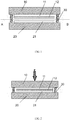
- Fig. 1 shows a fundamental structure of the impulse generator according to the present disclosure.
- the impulse generator comprises a first substrate 10; a first conductive film layer 11 on the first substrate; an insulation film layer 12 on the first conductive film layer; a second substrate 20; and a second conductive film layer 21 on the second substrate; and an elastic connection body 30.
- the elastic connection body 30 is used for connecting the first substrate 10 with the second substrate 20 such that the insulation film layer 12 and the second conductive film layer 21 face each other.
- the insulation film layer 12 is separated from the second conductive film layer 21; that is, the insulation film layer 12 is apart from the second conductive film layer 21 by a space.
- Fig. 2 when an external force F is applied on the first substrate 10 or the second substrate 21, the insulation film layer 12 is in contact with the second conductive film layer 21 such that, a surface charge transfer is generated between the insulation film 12 and the second conductive film layer 21.
- the second conductive film layer 12 preferably has the same shape as that of the insulation film layer 21 such that, when an external force is applied on the first substrate or the second substrate, the insulation film layer 12 is completely in contact with the second conductive film layer 21, as shown in Fig. 2 .
- the surface charge transfer generated between the insulation film 12 and the second conductive film layer 21 means that there is a difference in triboelectric series between the materials for the insulation film layer 12 and the second conductive film layer 21.
- triboelectric series means the materials are ordered by the degrees of their attraction to charge. At the moment when two materials contact with each other, positive charges on the contact surface are transferred from the surface of one material that has a relatively negative polarity in triboelectric series to the surface of the other material that has a relatively positive polarity in triboelectric series. So far, there is no uniform theory that interprets completely the mechanism of charge transfer. It is generally recognized that such charge transfer is related with the surface work function of a material, and the charge transfer is achieved by transfer of electrons or ions on the surfaces. It should be further explained that the charge transfer requires a contact, instead of a relative friction, between two materials.
- Fig. 3 shows an operating principle of the impulse generator according to the present disclosure.
- the insulation film layer 12 is separated from the second conductive film layer 21, as shown in (a) of Fig. 3 ; and, when an external force (which is shown by an arrow) is applied on the first substrate 12 or the second substrate 21, the insulation film layer 21 is brought in contact with the second conductive film layer 12, at that moment, a surface charge transfer is generated, to form a layer of surface contacting charges, as shown in (b) of Fig. 3 .
- the electrons will flow from the first conductive film layer 12 through an external circuit to a second conductive film layer 21 and positive charges are generated on the first conductive film layer 12, referring to an arrow shown in (c) of Fig. 3 .
- an instant pulse current which goes through the external circuit/the loads is generated.
- the electrons on the second conductive film layer 21 go back to the first conductive film layer 12, to generate a reverse direction instant current, referring to an arrow shown in (d) of Fig. 3 . In this way repeatedly, an AC impulse current is generated.
- the first conductive film layer is made of a conductive material, at the same time, as one electrode of the generator, there is no special requirement on kinds of the material for the first conductive film layer, metal films such as Cu, Al, etc. manufactured by methods such as electron beam evaporation, plasma sputtering, and so on, may be used.
- the second conductive film layer is made of a conductive material, at the same time, as the other electrode of the generator, there is no special requirement on kinds of the material for the second conductive film layer, metal films Cu, Al, etc. having flat and smooth surfaces, manufactured by methods such as electron beam evaporation, plasma sputtering, and so on, may be used.
- the insulation film layer is made of a non-conductive material which is required to have a relatively great polarity difference in triboelectric series from the second conductive film layer.
- Available materials for the insulation film include but are not limited to polytetrafluoroethylene film, polydimethylsiloxane (PDMS) film, and the like.
- non-deformable and rigid materials are used for the first substrate and the second substrate, in the present disclosure, there is no special requirement on kinds of the material for the first substrate and the second substrate as long as they can resist mechanical shocks, for example, organic glass sheet, PE sheet, PVC sheet, and the like.
- the elastic connection body is provided to connect and support the first substrate and the second substrate, and maintains the separation of the second conductive film layer from the insulation film layer by a space that is a distance between the insulation film layer and the second conductive film layer greater than a thickness of the insulation film layer, by one or more order of magnitude.
- Elastic materials such as one or more springs, organic elastomer and the likes, may be used for the elastic connection body. Figs.
- FIG. 1 and 2 only schematically show the elastic connection body in the form of springs. Shape and location of the elastic connection body depends on the shape of the first substrate, the first conductive film layer, the insulation film layer, the second substrate or the second conductive film layer. A configuration that a plurality of springs is around the insulation film layer may be used.
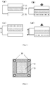
- Figs. 4 and 5 are sectional views along the broken line AB in Fig. 1 . Fig 4 is a sectional view showing an upper half of the impulse generator in Fig. 1 while Fig. 5 is a sectional view showing a lower half of the impulse generator in Fig. 1 .
- the insulation film layer 12 and the second conductive film layer 21 are both in the square shape and are respectively located in the middles of the first substrate 10 and the second substrate 20.
- the elastic connection body includes four springs respectively located around the insulation film layer 12 and the second conductive film layer 21 and connected with the first substrate 10 and the second substrate 20. Locations of the four springs preferably are located at the four apex corners of the square shaped insulation film layer 12 and second conductive film layer 21.
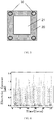
- the elastic connection body may also be configured that a ring of elastic material is attached to the second substrate around the second conductive film layer, for example, elastic rubber or spring around the second conductive film layer and used for connecting the first substrate with the second substrate.
- a ring of elastic material is attached to the second substrate around the second conductive film layer, for example, elastic rubber or spring around the second conductive film layer and used for connecting the first substrate with the second substrate.
- a metal copper film layer of 100nm in thickness and 5cm ⁇ 7cm in size may be used as the first conductive film layer
- a PDMS film layer of 10 micrometer in thickness and 5cm ⁇ 7cm in size may be used as the insulation film layer
- a metal aluminum film layer of 10 nm in thickness may be used as the second conductive film layer
- the first substrate and the second substrate are connected by springs.
- the PDMS material has a very negative polarity in triboelectric series while the metal aluminum has a relatively positive polarity in triboelectric series, combination of the materials in the present embodiment favours improvement of the output of the impulse generator.
- Fig. 6 shows a diagram of short-circuit current output, which has an instant current peak of about 2 mA, achieved when the first substrate or the second substrate of the impulse generator is beaten by the adult's palms.
- the impulse generator according to the present embodiment may be used to power up to 600 commercial LED light bulbs in real time, without any additional external power supplies.
- surface(s) of the second metallic film layer and/or the insulation film layer is/are physically modified to be distributed with microstructure array in micron or submicron dimension, in order to increase the contact area between the second metallic film layer and the insulation film layer so as to increase quantity of the contact charges.
- silicon slice is used as the second substrate and is spin coated with a layer of photoresist, a square window array with its side-length in micron or submicron dimension is formed on the photoresist by a lithographic process; the second substrate after implementation of the lithographic process is processed by a thermal chemical etching with potassium hydroxide, to form a array having a pyramid shaped depression structure, at the window; after that, a metal aluminum film is deposited by an evaporation or sputtering process to act as the second metallic film layer of the two kinds of contact materials.
- PDMS is used as the material for insulation film layer, and, when the two kinds of materials, i.e., the metal aluminum film and the PDMS, are in contact and squeezed with each other under the action of an external force, the depression structure may receive the PDMS and be filled with it due to good elasticity of the PDMS, thereby increasing the contact area compared with a smooth surface.
- an nanowires array is manufactured by implementing an inductive coupling plasma etching process on the surface of the insulation film layer, for example, aurum of about 10 nm in thickness is deposited on the surface of the insulation film layer by use of sputtering apparatus, after that, polyimide film is placed into an inductive coupling plasma etching machine, and the etching is implemented on the surface where the aurum is deposited, by providing a gas of O 2 , Ar and CF 4 with a flow rate of 10sccm, 15sccm, 30sccm, a pressure of 15mTorr, a working temperature of 55°C and a power of 400 watt, in order to produce the plasma, wherein the power of 100 watt is used to accelerate the plasma and the etching is sustained for about 5 minutes.
- an inductive coupling plasma etching process on the surface of the insulation film layer, for example, aurum of about 10 nm in thickness is deposited on the surface of the insulation film layer by use of sputtering
- surface(s) of the second metallic film layer and/or the insulation film layer is/are physically modified such that the surface(s) to be distributed with microstructure array in micron or submicron dimension, in order to increase the contact area between the second metallic film layer and the insulation film layer so as to increase quantity of the contact charges.
- surface(s) of the second metallic film layer and/or the insulation film layer in contact with each other is/are chemically modified to further increase quantity of the transferred charges at the contact moment, so as to improve density of the contact charges and output power of the impulse generator.
- chemical modifications There are two methods of chemical modifications as follows.
- a functional group i.e., a strong electron-donating group which is prone to lose electrons is introduced into a positive polarity material surface
- a functional group i.e., a strong electron-accepting group which is prone to accept electrons is introduced into a negative polarity material surface, either of which is capable of further increasing an amount of the transferred charges at the contact moment, so as to improve density of the contact charges and output power of the impulse generator.
- the strong electron donating group comprises amino group, hydroxyl group, alkoxy group and the like.
- the strong electron-accepting group comprises acyl group, carboxyl group, nitro group and the like.
- a metal aluminum film may be used as the second conductive film layer while a PDMS film may be used as the insulation film layer. It may further increase density of contact charges as the strong electron-accepting group is introduced into the PDMS surface.
- the method of introducing a strong electron-accepting group, such as nitro group, into the PDMS surface may include implementing a plasma surface modification process at an atmosphere of mixed gas of oxygen and nitrogen to produce the plasma under certain power, so as to achieve introduction of the amino group into the surface of polyimide.
- the other method is a chemical modification method of introducing positive charges into a positive polarity material surface while introducing negative charges into a negative polarity material surface.
- surface of the insulation film layer is modified with organic molecules by means of chemical key bonding, to electrify the insulation film layer with electric charges, for example, surface of a polydimethylsiloxane (PDMS) electrode is modified with tetraethl silicate (TEOS) by means of hydrolytic condensation (sol-gel), to electrify it with negative charges.
- surface of the second metallic film layer is modified with charged nano material, that is, to electrify the surface of the nano material with electric charges such that the second metallic film layer is electrified, for example, a metal film layer is modified with gold nanoparticles containing Cetyltrimethyl Ammonium Bromide (CTAB) on the surface thereof by means of gold-sulfur key bonding. As the Cetyltrimethyl Ammonium Bromide acts as positive ion, the whole second metallic film layer will become positive in electricity.
- CTAB Cetyltrimethyl Ammonium Bromide
- the present disclosure also provides an impulse generator set comprising a plurality of abovementioned impulse generators stacked vertically with one another.
- a first impulse generator is located on a second impulse generator, wherein the second substrate of the first impulse generator is the first substrate of the second impulse generator; and series connections and/or parallel connections are formed among the plurality of impulse generators. That is, the plurality of impulse generators are supposed vertically with one another and series connections and/or parallel connections are formed among the plurality of impulse generators, as a result, the achieved generator set may improve output power of the device, compared with the impulse generator.
- Fig. 8 shows one embodiment of the impulse generator set.
- the impulse generator set comprises impulse generators M1, M2 and M3.
- the impulse generator M2 is located on the impulse generator M3 while the impulse generator M1 is located on the impulse generator M2.
- the second substrate B1 of the first impulse generator M1 is the first substrate of the second impulse generator M2.
- the second substrate B2 of the first impulse generator M2 is the first substrate of the second impulse generator M3.
- one substrate is shared by two vertically adjacent impulse generators. Similar manner may be applied by analogy in these cases including more impulse generators, which is omitted herein.
- the first conductive film layers of all of the impulse generators are connected together through a conductive structure and the second conductive film layers of all of the impulse generators are connected together through a conductive structure, as a result, the achieved impulse generator set may be used as power supply for loads such as electrical appliances, electric batteries and the like.
- the conductive structure mentioned in the present disclosure may be common conductive materials, such as lead wire, metal film and the like.
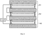
- Fig. 9 shows another embodiment of the impulse generator set.
- the impulse generator set comprises impulse generators N1, N2 and N3.
- the impulse generator N2 is located on the impulse generator N3 while the impulse generator N1 is located on the impulse generator N2.
- the stacked manner among the plurality of impulse generators is the same as that in Fig. 8 .
- Series connections are formed among the plurality of impulse generators, where, in two vertically adjacent impulse generators N1 and N2, the second conductive film layer of the first impulse generator N1 is connected with the first conductive film layer of the second impulse generator N2 through a conductive structure.
- the second conductive film layer of the second impulse generator N2 is connected with the first conductive film layer of the impulse generator N3 through a conductive structure.
- the achieved impulse generator set may be used as power supply for loads such as electrical appliances, electric batteries and the likes.
- the conductive structure mentioned in the present disclosure may be common conductive materials, such as lead wire, metal film and the like. Materials and configurations for the impulse generators of the impulse generator set according to the present disclosure may be the same, or else may be different.
- the impulse generator set according to the present disclosure may be further arranged along the horizontal direction, that is, the impulse generator sets shown in Fig. 8 or Fig. 9 are stacked along the horizontal direction, and series connections or parallel connections are formed among these impulse generator sets, forming an impulse generator set with greater output power.
- the impulse generator and the impulse generator set according to the present disclosure may convert external forces such as trample forces by feet and beating forces into electric energy for powering small appliances without any additional power supplies such as electric batteries. Accordingly, it is a simple and convenient electric generator. Moreover, the impulse generator and the impulse generator set according to the present disclosure are simple and convenient in manufacture process and low in manufacture cost and have wide applications.
Landscapes
- Micromachines (AREA)
- General Electrical Machinery Utilizing Piezoelectricity, Electrostriction Or Magnetostriction (AREA)
- Apparatus Associated With Microorganisms And Enzymes (AREA)
- Laminated Bodies (AREA)
Claims (15)
- Générateur d'impulsions comprenant
un premier substrat (10) ;
une première couche de film conducteur (11) sur le premier substrat (10) ;
une couche de film isolant (12) sur la première couche de film conducteur (11) ;
un second substrat (20) ;
une seconde couche de film conducteur (21) sur le second substrat (20) ; et
un corps de connexion élastique (30) pour connecter le premier substrat (10) au second substrat (20) de sorte que la couche de film isolant (12) et la seconde couche de film conducteur (21) soient l'une en face de l'autre ;
dans lequel, quand aucune force externe n'est appliquée sur le premier substrat (10) ou le second substrat (20), la couche de film isolant (12) est séparée de la seconde couche de film conducteur (21),
et, quand une force externe est appliquée sur le premier substrat (10) ou le second substrat (20), la couche de film isolant (12) entre en contact avec la seconde couche de film conducteur (21) pour générer un transfert de charge de surface entre la couche de film isolant (12) et la seconde couche de film conducteur (21), caractérisé en ce que quand aucune force externe n'est appliquée sur le premier substrat ou le second substrat, une distance entre la couche de film isolant et la seconde couche de film conducteur est supérieure d'un ou de plusieurs ordres de grandeur à une épaisseur de la couche de film isolant. - Générateur d'impulsions selon la revendication 1, dans lequel, la ou les surface(s) de la seconde couche de film conducteur (21) et/ou de la couche de film isolant (12) est/sont distribuée(s) avec un réseau de microstructure de dimension micrométrique ou sous-micrométrique.
- Générateur d'impulsions selon l'une des revendications 1 et 2, dans lequel, la ou les surface(s) de la seconde couche de film conducteur (21) et/ou de la couche de film isolant (12) est/sont chimiquement modifiée(s) de sorte qu'un groupe fonctionnel qui est enclin à perdre des électrons soit introduit dans une surface de matériau à polarité positive, ou qu'un fonctionnel qui est enclin à accepter des électrons soit introduit dans une surface de matériau à polarité négative.
- Générateur d'impulsions selon l'une des revendications 1 et 2, dans lequel, la ou les surface(s) de la seconde couche de film conducteur (21) et/ou de la couche de film isolant (12) est/sont chimiquement modifiée(s) de sorte que des charges positives soient introduites dans une surface de matériau à polarité positive et des charges négatives soient introduites dans une surface de matériau à polarité négative.
- Générateur d'impulsions selon l'une des revendications 1 à 4, dans lequel, la seconde couche de film conducteur (21) a la même forme que celle de la couche de film isolant (12) de sorte que, quand une force externe est appliquée sur le premier substrat (10) ou le second substrat (20), la couche de film isolant (12) soit complètement en contact avec la seconde couche de film conducteur (21).
- Générateur d'impulsions selon l'une des revendications 1 à 5, dans lequel, le corps de connexion élastique (30) comprend un ou plusieurs ressorts distribués autour de la couche de film isolant (12).
- Générateur d'impulsions selon l'une des revendications 1 à 6, dans lequel, le premier substrat (10) et/ou le second substrat (20) est (sont) une feuille de verre organique, une feuille de PE ou une feuille de PVC.
- Générateur d'impulsions selon l'une des revendications 1 à 6, dans lequel, la seconde couche de film conducteur (21) est une couche de film plat et lisse en aluminium métallique ou en cuivre métallique.
- Générateur d'impulsions selon l'une des revendications 1 à 8, dans lequel, la couche de film isolant (12) est un film de polytétrafluoroéthylène ou un film de polydiméthylsiloxane.
- Générateur d'impulsions selon l'une des revendications 1 à 9, dans lequel, la première couche de film conducteur (11) est une couche de film en aluminium métallique ou en cuivre métallique.
- Générateur d'impulsions selon l'une des revendications 1 à 4, dans lequel, la couche de film isolant (12) est un polydiméthylsiloxane et la seconde couche de film conducteur (21) est un film en aluminium métallique.
- Générateur d'impulsions selon l'une des revendications 1 à 4, dans lequel, le corps de connexion élastique (30) comprend un anneau de matériau élastique attaché au second substrat (20), autour de la seconde couche de film conducteur (21).
- Ensemble de générateurs d'impulsions, caractérisé en ce que, l'ensemble de générateurs d'impulsions comprend une pluralité de générateurs d'impulsions selon l'une des revendications 1 à 4 empilés verticalement les uns sur les autres, dans lequel,
dans chaque deux générateurs d'impulsions adjacents de la pluralité de générateurs d'impulsions, un premier générateur d'impulsions est sur un second générateur d'impulsions, dans lequel le second substrat (20) du premier générateur d'impulsions est le premier substrat (10) du second générateur d'impulsions ; et
des connexions en série et/ou des connexions en parallèle sont formées parmi la pluralité de générateurs d'impulsions. - Ensemble de générateurs d'impulsions selon la revendication 13, dans lequel, les premières couches de film conducteur (11) de la totalité de la pluralité de générateurs d'impulsions sont connectées conjointement par l'intermédiaire d'une structure conductrice, et les secondes couches de film conducteur (21) de la totalité de la pluralité de générateurs d'impulsions sont connectées conjointement par l'intermédiaire d'une structure conductrice.
- Ensemble de générateurs d'impulsions selon la revendication 13, dans lequel, dans chaque deux générateurs d'impulsions adjacents de la pluralité de générateurs d'impulsions, la seconde couche de film conducteur (21) du premier générateur d'impulsions est connectée à la première couche de film conducteur (11) du second générateur d'impulsions, par l'intermédiaire d'une structure conductrice.
Applications Claiming Priority (2)
| Application Number | Priority Date | Filing Date | Title |
|---|---|---|---|
| CN201210506295.0A CN103368458B (zh) | 2012-11-30 | 2012-11-30 | 脉冲发电机和发电机组 |
| PCT/CN2013/087820 WO2014082561A1 (fr) | 2012-11-30 | 2013-11-26 | Générateur d'impulsions et ensemble de générateurs |
Publications (3)
| Publication Number | Publication Date |
|---|---|
| EP2928063A1 EP2928063A1 (fr) | 2015-10-07 |
| EP2928063A4 EP2928063A4 (fr) | 2016-08-17 |
| EP2928063B1 true EP2928063B1 (fr) | 2019-11-13 |
Family
ID=49369153
Family Applications (1)
| Application Number | Title | Priority Date | Filing Date |
|---|---|---|---|
| EP13859243.1A Active EP2928063B1 (fr) | 2012-11-30 | 2013-11-26 | Générateur d'impulsions et ensemble de générateurs |
Country Status (6)
| Country | Link |
|---|---|
| US (1) | US9825557B2 (fr) |
| EP (1) | EP2928063B1 (fr) |
| JP (1) | JP6074567B2 (fr) |
| KR (1) | KR101797197B1 (fr) |
| CN (1) | CN103368458B (fr) |
| WO (1) | WO2014082561A1 (fr) |
Families Citing this family (41)
| Publication number | Priority date | Publication date | Assignee | Title |
|---|---|---|---|---|
| KR101358286B1 (ko) * | 2012-11-26 | 2014-02-12 | 서울대학교산학협력단 | 액체와의 접촉면 변화를 이용한 에너지 전환 장치 |
| CN103368458B (zh) * | 2012-11-30 | 2016-01-20 | 北京纳米能源与系统研究所 | 脉冲发电机和发电机组 |
| CN104836472B (zh) * | 2014-02-07 | 2017-11-03 | 北京纳米能源与系统研究所 | 利用声音能量的发电机和声音传感器 |
| CN104836473B (zh) * | 2014-02-07 | 2018-11-02 | 北京纳米能源与系统研究所 | 采集声音能量的发电机和声音传感器 |
| CN105091913B (zh) * | 2014-04-18 | 2018-02-16 | 北京纳米能源与系统研究所 | 基于静电感应的传感器和传感方法 |
| CN105099256B (zh) * | 2014-04-18 | 2017-10-10 | 北京纳米能源与系统研究所 | 基于静电感应的发电机和发电方法 |
| US9887644B2 (en) * | 2014-07-30 | 2018-02-06 | Seoul National University R&Db Foundation | Stretchable triboelectric generator, stretchable electricity storage device, and wearable electronic device |
| CN105490578B (zh) * | 2014-09-16 | 2018-01-02 | 北京纳米能源与系统研究所 | 一种接触分离式复合纳米发电机 |
| CN105450079B (zh) * | 2014-09-30 | 2019-05-17 | 北京纳米能源与系统研究所 | 振动能收集器及智能流量计 |
| KR101743674B1 (ko) * | 2014-11-11 | 2017-06-08 | 삼성전자주식회사 | 전하펌프 기반의 인공 번개 발전기 및 그 제조방법 |
| KR101685182B1 (ko) * | 2014-12-09 | 2016-12-12 | 한국과학기술원 | 접촉 대전 발전기 및 그 제조 방법 |
| CN104660095B (zh) | 2015-02-13 | 2018-09-28 | 京东方科技集团股份有限公司 | 一种摩擦发电装置及其制备方法 |
| CN104682768B (zh) * | 2015-03-19 | 2016-11-30 | 京东方科技集团股份有限公司 | 一种摩擦发电结构及显示装置 |
| CN104734558B (zh) * | 2015-03-25 | 2017-08-29 | 京东方科技集团股份有限公司 | 阴极基板的制造方法,阴极基板及摩擦发电装置 |
| CN104779832B (zh) * | 2015-03-26 | 2017-07-21 | 北京大学 | 一种高性能的摩擦发电机及其制备方法 |
| CN104702144A (zh) * | 2015-04-03 | 2015-06-10 | 京东方科技集团股份有限公司 | 摩擦发电机、摩擦发电装置及显示装置 |
| CN106301062B (zh) * | 2015-05-11 | 2019-04-30 | 北京纳米能源与系统研究所 | 可变形摩擦纳米发电机和发电方法、运动传感器和服装 |
| CN104811089A (zh) * | 2015-05-19 | 2015-07-29 | 京东方科技集团股份有限公司 | 一种摩擦生电装置及其制作方法、电子设备和可穿戴设备 |
| CN105099258B (zh) * | 2015-07-17 | 2017-04-26 | 纳智源科技(唐山)有限责任公司 | 具有嵌入式电极结构的摩擦发电机 |
| KR101788733B1 (ko) * | 2015-07-28 | 2017-11-15 | 충남대학교산학협력단 | 마찰 발전 소자 및 그 제조 방법 |
| CN105656344B (zh) * | 2016-03-02 | 2017-10-20 | 北京石油化工学院 | 一种基于介电弹性体的汽车轮胎发电装置 |
| KR102578823B1 (ko) * | 2016-05-10 | 2023-09-15 | 삼성전자주식회사 | 마찰전기 발전기 |
| US10770990B2 (en) | 2016-05-10 | 2020-09-08 | Samsung Electronics Co., Ltd. | Triboelectric generator |
| CN105978395B (zh) * | 2016-06-07 | 2018-11-23 | 清华大学 | 无基底电极驻极体静电直线发电机和制造该驻极体的方法 |
| CN105932899B (zh) * | 2016-06-07 | 2018-12-11 | 清华大学 | 无基底电极驻极体静电发电机和制造该驻极体的方法 |
| CN106253738B (zh) * | 2016-08-12 | 2019-04-05 | 王海清 | 一种高密度电荷电场发电机 |
| CN106585042B (zh) * | 2016-08-26 | 2018-10-23 | 纳智源科技(唐山)有限责任公司 | 摩擦发电机用复合薄膜电极及其制备方法和应用 |
| CN106655877B (zh) * | 2016-12-09 | 2019-02-01 | 北京纳米能源与系统研究所 | 一种发电机 |
| CN106739197B (zh) * | 2016-12-23 | 2019-05-10 | 北京纳米能源与系统研究所 | 波浪形复合薄膜及其成型设备、成型方法和摩擦发电机 |
| US10804818B2 (en) * | 2017-06-30 | 2020-10-13 | Toyota Motor Engineering & Manufacturing North America, Inc. | Triboelectric generator and network for mechanical energy harvesting |
| CN109747268B (zh) * | 2017-11-01 | 2020-06-16 | 北京纳米能源与系统研究所 | 基于摩擦纳米发电机的自驱动打印机 |
| CN108471219B (zh) * | 2018-04-08 | 2019-11-05 | 西北工业大学 | 一种非接触式可穿戴电磁-摩擦混合纳米发电装置及制备方法 |
| CN108429484B (zh) * | 2018-04-08 | 2019-08-09 | 西北工业大学 | 基于废弃氟化橡胶粉末的自供电纳米摩擦电发电机的制备方法 |
| KR20200137288A (ko) * | 2019-05-29 | 2020-12-09 | 한국전자기술연구원 | 출력 전달 효율성을 높이는 마찰전기 발전 장치 |
| CN112217414B (zh) * | 2020-09-10 | 2024-06-21 | 西南大学 | 一种基于微流道的摩擦纳米发电机及发电方法 |
| CN112031325A (zh) * | 2020-09-30 | 2020-12-04 | 忻州师范学院 | 一种摩擦发电地板、及其制备方法和应用 |
| CN112396721B (zh) * | 2020-10-23 | 2023-04-14 | 孙浴峰 | 一种海流动力发电式黑匣子 |
| CN112671259A (zh) * | 2021-01-12 | 2021-04-16 | 深圳大学 | 基于4d打印的摩擦纳米发电机、能量收集装置及制备方法 |
| CN113266524A (zh) * | 2021-05-14 | 2021-08-17 | 母志长 | 运行气流发电机 |
| CN114804016A (zh) * | 2022-04-26 | 2022-07-29 | 浙江大学 | 利用感应耦合等离子干法刻蚀提高摩擦电输出性能的方法 |
| JP2024135118A (ja) * | 2023-03-22 | 2024-10-04 | リンテック株式会社 | 振動発電装置 |
Family Cites Families (20)
| Publication number | Priority date | Publication date | Assignee | Title |
|---|---|---|---|---|
| NL133060B (fr) * | 1944-03-28 | |||
| JPS6032061A (ja) * | 1983-08-02 | 1985-02-19 | Mitsubishi Chem Ind Ltd | 磁性トナ− |
| JPH03179364A (ja) * | 1989-12-07 | 1991-08-05 | Sharp Corp | トナー及びその製造方法 |
| JPH10225145A (ja) * | 1997-02-13 | 1998-08-21 | Oki Electric Ind Co Ltd | 媒体搬送装置 |
| JP2001125221A (ja) * | 1999-10-26 | 2001-05-11 | Minolta Co Ltd | 画像形成方法 |
| FR2925792B1 (fr) * | 2007-12-21 | 2012-12-07 | Commissariat Energie Atomique | Dispositif de recuperation d'energie a electrode liquide |
| GB2463117A (en) * | 2008-09-08 | 2010-03-10 | Landa Lab Ltd | Generating electricity from the thermal motion of gas molecules |
| US9132693B2 (en) * | 2008-09-16 | 2015-09-15 | Koninklijke Philps N.V. | Capacitive micromachine ultrasound transducer |
| JP5578810B2 (ja) * | 2009-06-19 | 2014-08-27 | キヤノン株式会社 | 静電容量型の電気機械変換装置 |
| JP2011172366A (ja) * | 2010-02-17 | 2011-09-01 | Toyota Boshoku Corp | 発電マット |
| JP2012010564A (ja) | 2010-06-28 | 2012-01-12 | Toyota Boshoku Corp | 発電マット |
| CN102290968B (zh) * | 2011-06-17 | 2014-02-12 | 北京大学 | 一种微发电机及其制备方法 |
| CN102710166B (zh) * | 2012-04-13 | 2015-01-07 | 纳米新能源(唐山)有限责任公司 | 一种摩擦发电机 |
| CN102684546B (zh) * | 2012-05-15 | 2015-03-18 | 纳米新能源(唐山)有限责任公司 | 一种摩擦发电机 |
| JP5790601B2 (ja) * | 2012-07-19 | 2015-10-07 | オムロン株式会社 | 振動発電装置 |
| US9595894B2 (en) * | 2012-09-21 | 2017-03-14 | Georgia Tech Research Corporation | Triboelectric nanogenerator for powering portable electronics |
| CN103368458B (zh) | 2012-11-30 | 2016-01-20 | 北京纳米能源与系统研究所 | 脉冲发电机和发电机组 |
| KR101358295B1 (ko) * | 2012-12-21 | 2014-02-05 | 서울대학교산학협력단 | 액체를 이용한 에너지 전환 기판 |
| KR101445052B1 (ko) * | 2014-01-09 | 2014-09-26 | 성균관대학교산학협력단 | 3차원 뿔 형태의 정전기 에너지 발전 소자 |
| US10224539B2 (en) * | 2014-08-07 | 2019-03-05 | Council Of Scientific And Industrial Research | Surface modified cathode with improved lithium intercalation behavior |
-
2012
- 2012-11-30 CN CN201210506295.0A patent/CN103368458B/zh active Active
-
2013
- 2013-11-26 EP EP13859243.1A patent/EP2928063B1/fr active Active
- 2013-11-26 WO PCT/CN2013/087820 patent/WO2014082561A1/fr not_active Ceased
- 2013-11-26 JP JP2015544336A patent/JP6074567B2/ja active Active
- 2013-11-26 US US14/648,189 patent/US9825557B2/en active Active
- 2013-11-26 KR KR1020157017417A patent/KR101797197B1/ko active Active
Non-Patent Citations (1)
| Title |
|---|
| None * |
Also Published As
| Publication number | Publication date |
|---|---|
| CN103368458A (zh) | 2013-10-23 |
| WO2014082561A1 (fr) | 2014-06-05 |
| JP2016500248A (ja) | 2016-01-07 |
| KR20150091366A (ko) | 2015-08-10 |
| EP2928063A4 (fr) | 2016-08-17 |
| US9825557B2 (en) | 2017-11-21 |
| KR101797197B1 (ko) | 2017-11-13 |
| CN103368458B (zh) | 2016-01-20 |
| EP2928063A1 (fr) | 2015-10-07 |
| US20150311823A1 (en) | 2015-10-29 |
| JP6074567B2 (ja) | 2017-02-08 |
Similar Documents
| Publication | Publication Date | Title |
|---|---|---|
| EP2928063B1 (fr) | Générateur d'impulsions et ensemble de générateurs | |
| CN104868777B (zh) | 一种摩擦纳米发电机、发电机组和发电方法 | |
| KR101982691B1 (ko) | 슬라이드 마찰식 나노발전기 및 발전 방법 | |
| EP2975758B1 (fr) | Nanogénérateur frictionnel glissant et procédé de génération de puissance | |
| CN203851062U (zh) | 一种接触-分离式摩擦纳米发电机 | |
| CN103780127B (zh) | 一种摩擦纳米发电机 | |
| CN104283453B (zh) | 滑动摩擦发电机、发电方法以及矢量位移传感器 | |
| CN103780137B (zh) | 一种振动开关式摩擦发电机和摩擦发电方法 | |
| CN103780122B (zh) | 一种滑动式摩擦纳米发电机组 | |
| CN103368452B (zh) | 静电脉冲发电机和直流脉冲发电机 | |
| CN103368449B (zh) | 一种滑动摩擦纳米发电机 | |
| CN103368447B (zh) | 静电脉冲发电机和直流脉冲发电机 | |
| CN104426415B (zh) | 一种脉冲发电机、发电机组和能量收集装置 | |
| WO2014169724A1 (fr) | Nanogénérateur à friction éolien | |
| CN103780132B (zh) | 一种脉冲摩擦发电机和摩擦发电方法 | |
| CN104242723A (zh) | 单电极摩擦纳米发电机、发电方法和自驱动追踪装置 | |
| CN105099256B (zh) | 基于静电感应的发电机和发电方法 | |
| CN104253562B (zh) | 包围式单电极摩擦纳米发电机、发电方法和追踪装置 | |
| CN110572073A (zh) | 一种混合型摩擦纳米发电机 | |
| CN103368451A (zh) | 一种滑动摩擦纳米发电机 | |
| WO2014117683A1 (fr) | Ensemble générateur nanomètre à friction coulissant et dispositif de production d'énergie | |
| CN103780124B (zh) | 一种滑动式摩擦纳米发电机组 |
Legal Events
| Date | Code | Title | Description |
|---|---|---|---|
| PUAI | Public reference made under article 153(3) epc to a published international application that has entered the european phase |
Free format text: ORIGINAL CODE: 0009012 |
|
| 17P | Request for examination filed |
Effective date: 20150611 |
|
| AK | Designated contracting states |
Kind code of ref document: A1 Designated state(s): AL AT BE BG CH CY CZ DE DK EE ES FI FR GB GR HR HU IE IS IT LI LT LU LV MC MK MT NL NO PL PT RO RS SE SI SK SM TR |
|
| AX | Request for extension of the european patent |
Extension state: BA ME |
|
| DAX | Request for extension of the european patent (deleted) | ||
| RA4 | Supplementary search report drawn up and despatched (corrected) |
Effective date: 20160714 |
|
| RIC1 | Information provided on ipc code assigned before grant |
Ipc: H02N 1/04 20060101AFI20160708BHEP |
|
| GRAP | Despatch of communication of intention to grant a patent |
Free format text: ORIGINAL CODE: EPIDOSNIGR1 |
|
| STAA | Information on the status of an ep patent application or granted ep patent |
Free format text: STATUS: GRANT OF PATENT IS INTENDED |
|
| INTG | Intention to grant announced |
Effective date: 20190704 |
|
| GRAS | Grant fee paid |
Free format text: ORIGINAL CODE: EPIDOSNIGR3 |
|
| GRAA | (expected) grant |
Free format text: ORIGINAL CODE: 0009210 |
|
| STAA | Information on the status of an ep patent application or granted ep patent |
Free format text: STATUS: THE PATENT HAS BEEN GRANTED |
|
| AK | Designated contracting states |
Kind code of ref document: B1 Designated state(s): AL AT BE BG CH CY CZ DE DK EE ES FI FR GB GR HR HU IE IS IT LI LT LU LV MC MK MT NL NO PL PT RO RS SE SI SK SM TR |
|
| REG | Reference to a national code |
Ref country code: AT Ref legal event code: REF Ref document number: 1202717 Country of ref document: AT Kind code of ref document: T Effective date: 20191115 Ref country code: CH Ref legal event code: EP |
|
| REG | Reference to a national code |
Ref country code: DE Ref legal event code: R096 Ref document number: 602013062972 Country of ref document: DE |
|
| REG | Reference to a national code |
Ref country code: IE Ref legal event code: FG4D |
|
| REG | Reference to a national code |
Ref country code: NL Ref legal event code: MP Effective date: 20191113 |
|
| REG | Reference to a national code |
Ref country code: LT Ref legal event code: MG4D |
|
| PG25 | Lapsed in a contracting state [announced via postgrant information from national office to epo] |
Ref country code: GR Free format text: LAPSE BECAUSE OF FAILURE TO SUBMIT A TRANSLATION OF THE DESCRIPTION OR TO PAY THE FEE WITHIN THE PRESCRIBED TIME-LIMIT Effective date: 20200214 Ref country code: LT Free format text: LAPSE BECAUSE OF FAILURE TO SUBMIT A TRANSLATION OF THE DESCRIPTION OR TO PAY THE FEE WITHIN THE PRESCRIBED TIME-LIMIT Effective date: 20191113 Ref country code: PL Free format text: LAPSE BECAUSE OF FAILURE TO SUBMIT A TRANSLATION OF THE DESCRIPTION OR TO PAY THE FEE WITHIN THE PRESCRIBED TIME-LIMIT Effective date: 20191113 Ref country code: LV Free format text: LAPSE BECAUSE OF FAILURE TO SUBMIT A TRANSLATION OF THE DESCRIPTION OR TO PAY THE FEE WITHIN THE PRESCRIBED TIME-LIMIT Effective date: 20191113 Ref country code: PT Free format text: LAPSE BECAUSE OF FAILURE TO SUBMIT A TRANSLATION OF THE DESCRIPTION OR TO PAY THE FEE WITHIN THE PRESCRIBED TIME-LIMIT Effective date: 20200313 Ref country code: SE Free format text: LAPSE BECAUSE OF FAILURE TO SUBMIT A TRANSLATION OF THE DESCRIPTION OR TO PAY THE FEE WITHIN THE PRESCRIBED TIME-LIMIT Effective date: 20191113 Ref country code: NL Free format text: LAPSE BECAUSE OF FAILURE TO SUBMIT A TRANSLATION OF THE DESCRIPTION OR TO PAY THE FEE WITHIN THE PRESCRIBED TIME-LIMIT Effective date: 20191113 Ref country code: BG Free format text: LAPSE BECAUSE OF FAILURE TO SUBMIT A TRANSLATION OF THE DESCRIPTION OR TO PAY THE FEE WITHIN THE PRESCRIBED TIME-LIMIT Effective date: 20200213 Ref country code: NO Free format text: LAPSE BECAUSE OF FAILURE TO SUBMIT A TRANSLATION OF THE DESCRIPTION OR TO PAY THE FEE WITHIN THE PRESCRIBED TIME-LIMIT Effective date: 20200213 Ref country code: FI Free format text: LAPSE BECAUSE OF FAILURE TO SUBMIT A TRANSLATION OF THE DESCRIPTION OR TO PAY THE FEE WITHIN THE PRESCRIBED TIME-LIMIT Effective date: 20191113 |
|
| PG25 | Lapsed in a contracting state [announced via postgrant information from national office to epo] |
Ref country code: RS Free format text: LAPSE BECAUSE OF FAILURE TO SUBMIT A TRANSLATION OF THE DESCRIPTION OR TO PAY THE FEE WITHIN THE PRESCRIBED TIME-LIMIT Effective date: 20191113 Ref country code: HR Free format text: LAPSE BECAUSE OF FAILURE TO SUBMIT A TRANSLATION OF THE DESCRIPTION OR TO PAY THE FEE WITHIN THE PRESCRIBED TIME-LIMIT Effective date: 20191113 Ref country code: IS Free format text: LAPSE BECAUSE OF FAILURE TO SUBMIT A TRANSLATION OF THE DESCRIPTION OR TO PAY THE FEE WITHIN THE PRESCRIBED TIME-LIMIT Effective date: 20200313 |
|
| PG25 | Lapsed in a contracting state [announced via postgrant information from national office to epo] |
Ref country code: AL Free format text: LAPSE BECAUSE OF FAILURE TO SUBMIT A TRANSLATION OF THE DESCRIPTION OR TO PAY THE FEE WITHIN THE PRESCRIBED TIME-LIMIT Effective date: 20191113 |
|
| REG | Reference to a national code |
Ref country code: CH Ref legal event code: PL |
|
| PG25 | Lapsed in a contracting state [announced via postgrant information from national office to epo] |
Ref country code: CH Free format text: LAPSE BECAUSE OF NON-PAYMENT OF DUE FEES Effective date: 20191130 Ref country code: LI Free format text: LAPSE BECAUSE OF NON-PAYMENT OF DUE FEES Effective date: 20191130 Ref country code: RO Free format text: LAPSE BECAUSE OF FAILURE TO SUBMIT A TRANSLATION OF THE DESCRIPTION OR TO PAY THE FEE WITHIN THE PRESCRIBED TIME-LIMIT Effective date: 20191113 Ref country code: CZ Free format text: LAPSE BECAUSE OF FAILURE TO SUBMIT A TRANSLATION OF THE DESCRIPTION OR TO PAY THE FEE WITHIN THE PRESCRIBED TIME-LIMIT Effective date: 20191113 Ref country code: ES Free format text: LAPSE BECAUSE OF FAILURE TO SUBMIT A TRANSLATION OF THE DESCRIPTION OR TO PAY THE FEE WITHIN THE PRESCRIBED TIME-LIMIT Effective date: 20191113 Ref country code: EE Free format text: LAPSE BECAUSE OF FAILURE TO SUBMIT A TRANSLATION OF THE DESCRIPTION OR TO PAY THE FEE WITHIN THE PRESCRIBED TIME-LIMIT Effective date: 20191113 Ref country code: DK Free format text: LAPSE BECAUSE OF FAILURE TO SUBMIT A TRANSLATION OF THE DESCRIPTION OR TO PAY THE FEE WITHIN THE PRESCRIBED TIME-LIMIT Effective date: 20191113 Ref country code: LU Free format text: LAPSE BECAUSE OF NON-PAYMENT OF DUE FEES Effective date: 20191126 |
|
| REG | Reference to a national code |
Ref country code: DE Ref legal event code: R097 Ref document number: 602013062972 Country of ref document: DE |
|
| REG | Reference to a national code |
Ref country code: AT Ref legal event code: MK05 Ref document number: 1202717 Country of ref document: AT Kind code of ref document: T Effective date: 20191113 |
|
| REG | Reference to a national code |
Ref country code: BE Ref legal event code: MM Effective date: 20191130 |
|
| PG25 | Lapsed in a contracting state [announced via postgrant information from national office to epo] |
Ref country code: SM Free format text: LAPSE BECAUSE OF FAILURE TO SUBMIT A TRANSLATION OF THE DESCRIPTION OR TO PAY THE FEE WITHIN THE PRESCRIBED TIME-LIMIT Effective date: 20191113 Ref country code: SK Free format text: LAPSE BECAUSE OF FAILURE TO SUBMIT A TRANSLATION OF THE DESCRIPTION OR TO PAY THE FEE WITHIN THE PRESCRIBED TIME-LIMIT Effective date: 20191113 Ref country code: MC Free format text: LAPSE BECAUSE OF FAILURE TO SUBMIT A TRANSLATION OF THE DESCRIPTION OR TO PAY THE FEE WITHIN THE PRESCRIBED TIME-LIMIT Effective date: 20191113 |
|
| PLBE | No opposition filed within time limit |
Free format text: ORIGINAL CODE: 0009261 |
|
| STAA | Information on the status of an ep patent application or granted ep patent |
Free format text: STATUS: NO OPPOSITION FILED WITHIN TIME LIMIT |
|
| 26N | No opposition filed |
Effective date: 20200814 |
|
| PG25 | Lapsed in a contracting state [announced via postgrant information from national office to epo] |
Ref country code: IE Free format text: LAPSE BECAUSE OF NON-PAYMENT OF DUE FEES Effective date: 20191126 |
|
| PG25 | Lapsed in a contracting state [announced via postgrant information from national office to epo] |
Ref country code: SI Free format text: LAPSE BECAUSE OF FAILURE TO SUBMIT A TRANSLATION OF THE DESCRIPTION OR TO PAY THE FEE WITHIN THE PRESCRIBED TIME-LIMIT Effective date: 20191113 Ref country code: AT Free format text: LAPSE BECAUSE OF FAILURE TO SUBMIT A TRANSLATION OF THE DESCRIPTION OR TO PAY THE FEE WITHIN THE PRESCRIBED TIME-LIMIT Effective date: 20191113 Ref country code: BE Free format text: LAPSE BECAUSE OF NON-PAYMENT OF DUE FEES Effective date: 20191130 |
|
| PG25 | Lapsed in a contracting state [announced via postgrant information from national office to epo] |
Ref country code: IT Free format text: LAPSE BECAUSE OF FAILURE TO SUBMIT A TRANSLATION OF THE DESCRIPTION OR TO PAY THE FEE WITHIN THE PRESCRIBED TIME-LIMIT Effective date: 20191113 |
|
| PG25 | Lapsed in a contracting state [announced via postgrant information from national office to epo] |
Ref country code: CY Free format text: LAPSE BECAUSE OF FAILURE TO SUBMIT A TRANSLATION OF THE DESCRIPTION OR TO PAY THE FEE WITHIN THE PRESCRIBED TIME-LIMIT Effective date: 20191113 |
|
| PG25 | Lapsed in a contracting state [announced via postgrant information from national office to epo] |
Ref country code: MT Free format text: LAPSE BECAUSE OF FAILURE TO SUBMIT A TRANSLATION OF THE DESCRIPTION OR TO PAY THE FEE WITHIN THE PRESCRIBED TIME-LIMIT Effective date: 20191113 Ref country code: HU Free format text: LAPSE BECAUSE OF FAILURE TO SUBMIT A TRANSLATION OF THE DESCRIPTION OR TO PAY THE FEE WITHIN THE PRESCRIBED TIME-LIMIT; INVALID AB INITIO Effective date: 20131126 |
|
| PG25 | Lapsed in a contracting state [announced via postgrant information from national office to epo] |
Ref country code: TR Free format text: LAPSE BECAUSE OF FAILURE TO SUBMIT A TRANSLATION OF THE DESCRIPTION OR TO PAY THE FEE WITHIN THE PRESCRIBED TIME-LIMIT Effective date: 20191113 |
|
| PG25 | Lapsed in a contracting state [announced via postgrant information from national office to epo] |
Ref country code: MK Free format text: LAPSE BECAUSE OF FAILURE TO SUBMIT A TRANSLATION OF THE DESCRIPTION OR TO PAY THE FEE WITHIN THE PRESCRIBED TIME-LIMIT Effective date: 20191113 |
|
| REG | Reference to a national code |
Ref country code: DE Ref legal event code: R082 Ref document number: 602013062972 Country of ref document: DE Representative=s name: MATHYS & SQUIRE EUROPE PATENTANWAELTE PARTNERS, DE |
|
| PGFP | Annual fee paid to national office [announced via postgrant information from national office to epo] |
Ref country code: DE Payment date: 20251118 Year of fee payment: 13 |
|
| PGFP | Annual fee paid to national office [announced via postgrant information from national office to epo] |
Ref country code: GB Payment date: 20251010 Year of fee payment: 13 |
|
| PGFP | Annual fee paid to national office [announced via postgrant information from national office to epo] |
Ref country code: FR Payment date: 20251010 Year of fee payment: 13 |