EP2929312B1 - Eine temperaturfühlerperipherie - Google Patents
Eine temperaturfühlerperipherie Download PDFInfo
- Publication number
- EP2929312B1 EP2929312B1 EP13811744.5A EP13811744A EP2929312B1 EP 2929312 B1 EP2929312 B1 EP 2929312B1 EP 13811744 A EP13811744 A EP 13811744A EP 2929312 B1 EP2929312 B1 EP 2929312B1
- Authority
- EP
- European Patent Office
- Prior art keywords
- temperature
- voltage
- integrated circuit
- operational amplifier
- mixed signal
- Prior art date
- Legal status (The legal status is an assumption and is not a legal conclusion. Google has not performed a legal analysis and makes no representation as to the accuracy of the status listed.)
- Not-in-force
Links
- 230000002093 peripheral effect Effects 0.000 title description 26
- 230000006870 function Effects 0.000 claims description 5
- 238000009529 body temperature measurement Methods 0.000 claims description 3
- 239000004065 semiconductor Substances 0.000 claims description 2
- 238000010586 diagram Methods 0.000 description 13
- 230000008859 change Effects 0.000 description 12
- 238000000034 method Methods 0.000 description 5
- 239000000523 sample Substances 0.000 description 5
- 230000001419 dependent effect Effects 0.000 description 4
- 230000004048 modification Effects 0.000 description 3
- 238000012986 modification Methods 0.000 description 3
- 230000008901 benefit Effects 0.000 description 2
- 238000013461 design Methods 0.000 description 2
- 230000003993 interaction Effects 0.000 description 2
- 230000008569 process Effects 0.000 description 2
- 230000004075 alteration Effects 0.000 description 1
- 238000006243 chemical reaction Methods 0.000 description 1
- 239000002131 composite material Substances 0.000 description 1
- 230000008878 coupling Effects 0.000 description 1
- 238000010168 coupling process Methods 0.000 description 1
- 238000005859 coupling reaction Methods 0.000 description 1
- 238000001514 detection method Methods 0.000 description 1
- 238000005516 engineering process Methods 0.000 description 1
- 238000012545 processing Methods 0.000 description 1
Images



Classifications
-
- G—PHYSICS
- G01—MEASURING; TESTING
- G01K—MEASURING TEMPERATURE; MEASURING QUANTITY OF HEAT; THERMALLY-SENSITIVE ELEMENTS NOT OTHERWISE PROVIDED FOR
- G01K15/00—Testing or calibrating of thermometers
- G01K15/005—Calibration
-
- G—PHYSICS
- G01—MEASURING; TESTING
- G01K—MEASURING TEMPERATURE; MEASURING QUANTITY OF HEAT; THERMALLY-SENSITIVE ELEMENTS NOT OTHERWISE PROVIDED FOR
- G01K7/00—Measuring temperature based on the use of electric or magnetic elements directly sensitive to heat ; Power supply therefor, e.g. using thermoelectric elements
- G01K7/01—Measuring temperature based on the use of electric or magnetic elements directly sensitive to heat ; Power supply therefor, e.g. using thermoelectric elements using semiconducting elements having PN junctions
-
- G—PHYSICS
- G01—MEASURING; TESTING
- G01K—MEASURING TEMPERATURE; MEASURING QUANTITY OF HEAT; THERMALLY-SENSITIVE ELEMENTS NOT OTHERWISE PROVIDED FOR
- G01K7/00—Measuring temperature based on the use of electric or magnetic elements directly sensitive to heat ; Power supply therefor, e.g. using thermoelectric elements
- G01K7/16—Measuring temperature based on the use of electric or magnetic elements directly sensitive to heat ; Power supply therefor, e.g. using thermoelectric elements using resistive elements
- G01K7/18—Measuring temperature based on the use of electric or magnetic elements directly sensitive to heat ; Power supply therefor, e.g. using thermoelectric elements using resistive elements the element being a linear resistance, e.g. platinum resistance thermometer
- G01K7/20—Measuring temperature based on the use of electric or magnetic elements directly sensitive to heat ; Power supply therefor, e.g. using thermoelectric elements using resistive elements the element being a linear resistance, e.g. platinum resistance thermometer in a specially-adapted circuit, e.g. bridge circuit
- G01K7/21—Measuring temperature based on the use of electric or magnetic elements directly sensitive to heat ; Power supply therefor, e.g. using thermoelectric elements using resistive elements the element being a linear resistance, e.g. platinum resistance thermometer in a specially-adapted circuit, e.g. bridge circuit for modifying the output characteristic, e.g. linearising
Definitions
- the present disclosure relates to temperature sensing apparatus, and, in particular, a temperature sensor peripheral having independent temperature coefficient and offset adjustment programmability.
- US Patent Application Publication US 2006/0103449 discloses a semiconductor integrated circuit device with a temperature detection function.
- US Patent US 6,377,110 discloses a low cost temperature sensor providing relatively high accuracy, a wide dynamic range and high linearity.
- a temperature sensor peripheral used in integrated circuit (IC) micro-controllers that can generate a voltage that may be used for purposes external to the IC and that is: a) proportional to temperature, b) whose temperature coefficient can be adjusted at the temperature probe to any desired value, c) whose temperature coefficient can be either positive or negative, d) whose room temperature voltage can be adjusted at the temperature probe to any desired value, and e) whose temperature coefficient and room temperature voltage are completely independent of one another.
- IC integrated circuit
- a method for measuring temperatures and producing voltages representative thereof may comprise the steps of: determining a first voltage representing a first calibration temperature; adjusting a first output voltage from a temperature sensor peripheral to equal the first voltage when a temperature sensor may be at the first calibration temperature; determining a range of voltages to represent a range of temperatures, wherein the first voltage may be within the range of voltages and the first calibration temperature may be within the range of temperatures; determining a second voltage representing a second calibration temperature within the range of temperatures; and adjusting a second output voltage from the temperature sensor peripheral to equal the second voltage when the temperature sensor may be at the second calibration temperature.
- the first voltage may be equal to a reference voltage coupled to an input of an operational amplifier of the temperature sensor peripheral.
- the first calibration temperature may be room temperature.
- a circuit may be provided that generates a voltage proportional to temperature and whose temperature coefficient, polarity of temperature coefficient and room temperature voltage are independently user selectable.
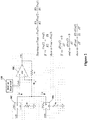
- An operational amplifier 106 has a negative input coupled to the outputs of the first and second voltage-to-current converters 102 and 104, a positive input coupled to a third reference voltage Vref3 and a resistor R3 coupled between an output and the negative input of the operational amplifier 106.
- the first and second reference voltages may or may not have the same temperature coefficient (TC).
- One of the reference voltages may be provided by a voltage reference having substantially no temperature coefficient (TC), e.g., substantially the same output voltage over all temperatures of operation, e.g ., a bandgap voltage reference, etc.
- the other reference voltage may be provided by a temperature measurement sensor, e.g ., diode junction, resistance temperature detector (RTD), thermistor, etc., having either a positive or negative temperature coefficient (TC).
- a temperature measurement sensor e.g ., diode junction, resistance temperature detector (RTD), thermistor, etc.
- RTD resistance temperature detector
- TC temperature coefficient
- Any one or more of the reference voltages, e.g ., Vref3, Vref2; or Vref3, Vref1; may be provided by a digital-to-analog converter (DAC) 108.
- DAC digital-to-analog converter
- the first current I1 from the first voltage-to-current converter 102 may be adjusted with a first resistor R1 coupled to a current adjustment input thereof.
- the second output current I2 from the second voltage-to-current converter 104 may be adjusted with a second resistor R2 coupled to a current adjustment input thereof.
- FIG. 1 Shown in Figure 1 are the mathematical relationships between the output voltage Vout from the operational amplifier 106; the first, second and third voltage references Vref1, Vref2 and Vref3; and the first, second and third resistors R1, R2 and R3. Also shown is the mathematical relationship of a change in output voltage dVout in relation to a change in temperature dT.
- a dVref term(s) is (are) substantially zero, then only the non-zero dVref term determines dVout/dT, after Vout has been adjusted to substantially equal Vref3, as more fully described hereinafter.
- two currents I1 and I2 having different temperature coefficients, one negative and the other positive, may be generated then summed together and the resultant current 13 converted back to a voltage Vout.
- a reliable output voltage with a well defined temperature coefficient may be provided.
- Either the first reference voltage Vref1 or the second reference voltage Vref2 may be controlled by a temperature sensor, e.g ., diode junction, resistance temperature detector (RTD), thermistor, etc.
- a temperature sensor e.g ., diode junction, resistance temperature detector (RTD), thermistor, etc.
- Appropriate temperature-to-voltage conversion may be provided by controlling the second reference voltage Vref2 with a temperature sensor having a positive temperature coefficient, or controlling the first reference voltage Vref1 with a temperature sensor having a negative temperature coefficient.
- first and second reference voltages Vref1 and/or Vref2 may vary with temperature and the circuit described hereinabove adjusted in such a way that the output voltage Vout thereof may be used for voltage controlled temperature compensation of another circuit that may need either positive or negative temperature compensation, e.g ., a voltage controlled oscillator having frequency determining components when coupled together have either a positive or negative temperature coefficient that must be compensated for over an operating temperature range.
- a voltage controlled oscillator having frequency determining components when coupled together have either a positive or negative temperature coefficient that must be compensated for over an operating temperature range.
- Another feature of the present invention is completely independent output voltage adjustment (output voltage offset) and voltage/temperature coefficient adjustment (range of dVout/dT) when the output voltage Vout is adjusted to be substantially equal to the third reference voltage Vref at a first calibration temperature. For example, first determine what output voltage range is required over the temperature range of interest. Then determine what the output voltage Vout of that voltage range would be at room temperature, e.g ., 27 degrees Centigrade (°C). Then set the third reference voltage Vref3 to that voltage, or use an existing third reference voltage Vref3 to define the first calibration voltage, e.g ., Vout at a first calibration temperature, e.g ., room temperature.
- Output voltage change dVout versus temperature change dT may be determined next.
- the second temperature adjust the third resistor R3 so that the output voltage Vout is at substantially the calculated output voltage of the second calibration temperature.
- FIG. 2 depicted is a schematic diagram of the temperature sensor peripheral shown in Figure 1 and circuit voltage relationships thereof.
- I1 I2, Vref2 and Vref3 do not change with temperature. If this is the case then the room temperature voltage may be set by adjusting the second resistor R2 so that the first current I1 equals the second current 12 and the temperature coefficient may be changed by adjusting the third resistor R3. In this example the first resistor R1 is held constant since it shows up in both the Vout and dVout/dT equations.
- FIG. 3 and 4 depicted is a schematic diagram of a temperature sensor peripheral, temperature sensor probe connected thereto and circuit voltage relationships thereof, according to another specific example embodiment of this disclosure.
- a second operational amplifier 308, and transistors 316 and 318 may function as the first and second voltage-to-current converters 102 and 104 shown in Figures 1 and 2 .
- the second reference voltage Vref2 will automatically be substantially the same voltage as the third reference voltage Vref3 due to operation of the operational amplifier 106 with the feedback resistor R3. Circuit function, adjustment and operation thereof may be substantially the same as described hereinabove for Figures 1 and 2 .
- a diode temperature sensor 314 may be coupled to a current source 312 and a resulting diode junction voltage Vbe dependent upon temperature may be coupled to a positive input of the operational amplifier 308. Since the third reference voltage Vref3 remains constant, e.g., from a band gap voltage reference (not shown) or a DAC 108, etc., the change in output voltage dVout is dependent only upon the change in the diode junction voltage dVbe. Voltage output Vout, offset and range may be adjusted as described hereinabove for a desired room temperature output voltage (first calibration output voltage at a first calibration temperature) and a desired dVout/dT (based upon a second calibration voltage at a second calibration temperature).
- any temperature sensor providing a voltage output corresponding to a temperature may be utilized, and one having ordinary skill in electronic circuit design and the benefit of this disclosure would readily understand how to implement such temperature sensors in combination with the teachings of this disclosure.
- FIG. 5 depicted is a schematic diagram of the temperature sensor peripheral shown in Figures 3 and 4 with exemplary component values and circuit voltage relationships thereof, according to the teachings of this disclosure.
- the calculated voltage and component values shown are derived at room temperature.
- a first voltage representing a first calibration temperature is selected.
- a first output voltage is adjusted to the first voltage while the temperature sensor is at the first calibration temperature.
- Vref3 to be the first (trim) voltage, or visa versa, to represent the first calibration temperature, e.g ., "room temperature” at the temperature sensor 314 (probe)
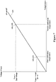
- a range of voltages representing a range of temperatures is determined, e.g ., slope dVout/dT (see Figure 7 ), wherein the first voltage is within the range of voltages.
- a second voltage representing a second calibration temperature within the range of temperatures is determined.
- the temperature sensor peripheral is adjusted so that a second output voltage therefrom is substantially the same as the second voltage while the temperature sensor 314 is at the second calibration temperature.
- This sequence of two calibration adjustments first setting the output voltage Vout to the reference voltage Vref3 while the temperature sensor 314 is at the first calibration temperature (e.g ., room temperature) determines the output voltage offset, and next setting the output voltage Vout to the second voltage while the temperature sensor 314 is at the second calibration temperature, e.g ., second calibration temperature different than the first calibration temperature, determines the slope of the change in output voltage dVout versus change in temperature dT with substantially no interaction between these two calibration adjustments.
- first calibration temperature e.g ., room temperature
- any output voltage offset may be selected, e.g., by using a digital-to-analog converter (DAC) 108 to generate Vref3.
- DAC digital-to-analog converter
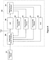
- a mixed signal integrated circuit 802 e.g., a microcontroller, may comprise a temperature sensor peripheral 808, an analog-to-digital converter (ADC) 806, a digital processor and memory 804, a digital-to-analog converter (DAC) 816, and programmable resistors 810, 812 and 814.
- a temperature sensor 314 may be coupled to an input of the temperature sensor peripheral 808, and an output voltage Vout may be provided from the temperature sensor peripheral 808. The output voltage Vout may be available for coupling to an external device and/or supplied to the ADC 806 for further processing by the digital processor 804.
- the DAC 816 may provide a reference voltage Vref3 to the temperature sensor peripheral 808, and programmable resistors 810, 812 and/or 814 may be used to provide output voltage offset and dVout/dT slope calibration, as more fully described hereinabove.
Landscapes
- Physics & Mathematics (AREA)
- General Physics & Mathematics (AREA)
- Measuring Temperature Or Quantity Of Heat (AREA)
- Measurement Of Current Or Voltage (AREA)
- Measuring Instrument Details And Bridges, And Automatic Balancing Devices (AREA)
- Indication And Recording Devices For Special Purposes And Tariff Metering Devices (AREA)
Claims (13)
- Integrierte Mischsignalschaltung, die einen Digitalprozessor und Speicher (804) aufweist; einen mit dem Digitalprozessor (804) gekoppelten Analog-Digital-Wandler (806) und eine Temperaturmessschaltung, die aufweist:einen ersten Operationsverstärker (106), der erste und zweite Eingänge und einen Ausgang aufweist,einen dritten Widerstand (R3), der zwischen dem Ausgang und dem zweiten Eingang des ersten Operationsverstärkers (106) gekoppelt ist,einen zweiten Operationsverstärker (308), der erste und zweite Eingänge und einen Ausgang aufweist,erste und zweite Transistoren (316, 318), die miteinander gekoppelte Source-Anschlüsse aufweisen, Gate-Anschlüsse, die mit einem Ausgang des zweiten Operationsverstärkers (308) gekoppelt sind, und Drain-Anschlüsse, die über erste und zweite Widerstände (R1; R2) mit Masse gekoppelt sind, wobei ein erster Knotenpunkt zwischen dem Drain-Anschluss des ersten Transistors (316) und dem ersten Widerstand (R1) mit dem zweiten Eingang des zweiten Operationsverstärkers (308) gekoppelt ist und ein zweiter Knotenpunkt zwischen dem Drain-Anschluss des zweiten Transistors (318) und dem zweiten Widerstand (R2) mit dem zweiten Eingang des ersten Operationsverstärkers (308) gekoppelt ist;wobei der erste Eingang des zweiten Operationsverstärkers (308) konfiguriert ist mit einem Temperatursensor (314) gekoppelt zu werden, und eine Referenzspannung (108) mit dem ersten Eingang des ersten Operationsverstärkers (106) gekoppelt ist;wobei der Ausgang des ersten Operationsverstärkers (106) eine Ausgangsspannung bereitstellt, die proportional zu einer durch den Temperatursensor (314) gemessenen Temperatur ist,wobei ein Eingang des Analog-Digital-Wandlers (806) konfiguriert ist eine Ausgangsspannung des ersten Operationsverstärkers (106) zu empfangen, wobei die ersten, zweiten und dritten Widerstände programmierbare Widerstände (810, 812, 814) sind und durch den Digitalprozessor (804) gesteuert werden.
- Integrierte Mischsignalschaltungsanordnung gemäß Anspruch 1, wobei der erste Eingang des ersten Operationsverstärkers (106) ein positiver Eingang ist und der zweite Eingang von diesem ein negativer Eingang ist.
- Integrierte Mischsignalschaltung gemäß Anspruch 1 oder 2, die weiterhin einen Digital-Analog-Wandler, DAC, (108) aufweist der konfiguriert ist, die Referenzspannung zu erzeugen, wobei der DAC (108) durch den Digitalprozessor (804) gesteuert wird.
- Integrierte Mischsignalschaltung gemäß einem der vorherigen Ansprüche, wobei eine Ausgangsspannung des ersten Operationsverstärkers (106) gleich einem Spannungswert an dem zweite Knotenpunkt multipliziert mit dem dritten Widerstandswert dividiert durch den zweiten Widerstandswert minus einem durch den Temperatursensor bereitgestellten Spannungswert multipliziert mit dem dritten Widerstandswert dividiert durch den ersten Widerstandswert plus dem Referenzspannungwert ist.
- Integrierte Mischsignalschaltung gemäß einem der vorherigen Ansprüche, wobei der Temperatursensor eine Spannungsausgabe proportional zu einer Temperatur von diesem aufweist, und die Referenzspannung mit Temperaturkoeffizienten bereitgestellt wird, die im Wesentlichen null betragen.
- Integrierte Mischsignalschaltung gemäß einem der vorherigen Ansprüche, wobei:die Referenzspannung und der zweite Widerstandswert eine erste Ausgangsspannung bestimmen, die eine erste Kalibrierungstemperatur repräsentiert, undder dritte Widerstandswert eine zweite Ausgangsspannung bestimmt, die eine zweite Kalibrierungstemperatur repräsentiert.
- Integrierte Mischsignalschaltung gemäß Anspruch 6, wobei die erste Kalibrierungstemperatur Raumtemperatur entspricht.
- Integrierte Mischsignalschaltung gemäß Anspruch 6 oder 7, wobei der Temperatursensor eine Halbleiterdiode ist, die mit einer Konstantstromquelle (312) gekoppelt ist und als eine Funktion der Temperatur eine Diodensperrschichtspannung bereitstellt.
- Integrierte Mischsignalschaltung gemäß Anspruch 6 oder 7, wobei der Temperatursensor ein Widerstandstemperaturdetektor ist.
- Integrierte Mischsignalschaltung gemäß Anspruch 6 oder 7, wobei der Temperatursensor ein Thermistor ist.
- Integrierte Mischsignalschaltung gemäß einem der vorherigen Ansprüche, wobei der Digitalprozessor (804) konfiguriert ist, den zweiten Widerstand (R2) so einzustellen, dass eine Spannung des Ausgangs des ersten Operationsverstärkers (106) gleich der Referenzspannung ist, und der zweite Strom gleich dem ersten Strom ist.
- Integrierte Mischsignalschaltung gemäß Anspruch 1, wobei die Referenzspannung durch eine programmierbare Referenzspannung (816) bereitgestellt wird, die mit dem Digitalprozessor (804) gekoppelt ist.
- Integrierte Mischsignalschaltung gemäß einem der vorherigen Ansprüche, wobei die integrierte Mischsignalschaltung ein Mikrocontroller ist.
Applications Claiming Priority (3)
| Application Number | Priority Date | Filing Date | Title |
|---|---|---|---|
| US201261735243P | 2012-12-10 | 2012-12-10 | |
| US14/097,405 US9739669B2 (en) | 2012-12-10 | 2013-12-05 | Temperature sensor peripheral having independent temperature coefficient and offset adjustment programmability |
| PCT/US2013/074015 WO2014093283A2 (en) | 2012-12-10 | 2013-12-10 | A temperature sensor peripheral having independent temperature coefficient and offset adjustment programmability |
Publications (2)
| Publication Number | Publication Date |
|---|---|
| EP2929312A2 EP2929312A2 (de) | 2015-10-14 |
| EP2929312B1 true EP2929312B1 (de) | 2018-05-09 |
Family
ID=50880935
Family Applications (1)
| Application Number | Title | Priority Date | Filing Date |
|---|---|---|---|
| EP13811744.5A Not-in-force EP2929312B1 (de) | 2012-12-10 | 2013-12-10 | Eine temperaturfühlerperipherie |
Country Status (4)
| Country | Link |
|---|---|
| US (2) | US9739669B2 (de) |
| EP (1) | EP2929312B1 (de) |
| CN (1) | CN104903689A (de) |
| WO (1) | WO2014093283A2 (de) |
Families Citing this family (16)
| Publication number | Priority date | Publication date | Assignee | Title |
|---|---|---|---|---|
| US20150346037A1 (en) * | 2014-05-29 | 2015-12-03 | Infineon Technologies Ag | Integrated temperature sensor |
| KR102373545B1 (ko) * | 2015-11-23 | 2022-03-11 | 삼성전자주식회사 | 온도 계수에 기초하여 기준 전압을 생성하는 회로 및 방법 |
| US10228294B2 (en) * | 2016-05-12 | 2019-03-12 | Infineon Technologies Ag | System and method for temperature sensing |
| US10295416B2 (en) * | 2016-10-10 | 2019-05-21 | Stmicroelectronics International N.V. | Temperature sensing circuit with temperature coefficient estimation and compensation using time variable substrate heating |
| KR20190029896A (ko) * | 2017-09-13 | 2019-03-21 | 에스케이하이닉스 주식회사 | 온도 센싱 회로 |
| US10824180B2 (en) | 2018-02-05 | 2020-11-03 | Abb Power Electronics Inc. | Systems and methods for improving current sharing between paralleled DC-to-DC power converters based on temperature coefficient |
| TWI671617B (zh) | 2018-07-09 | 2019-09-11 | 華邦電子股份有限公司 | 電流產生電路 |
| WO2020263175A1 (en) | 2019-06-25 | 2020-12-30 | Choon How Lau | Circuit arrangement and method of forming the same |
| KR102731715B1 (ko) * | 2019-09-16 | 2024-11-18 | 주식회사 엘엑스세미콘 | 온도센서를 구비한 소스드라이버 및 표시장치 |
| CN111272313B (zh) * | 2020-03-02 | 2025-03-07 | 苏州纳芯微电子股份有限公司 | 温度传感器组件 |
| CN113465764B (zh) * | 2020-03-31 | 2023-01-10 | 圣邦微电子(北京)股份有限公司 | 一种模拟输出集成温度传感器 |
| CN114520653A (zh) * | 2020-11-20 | 2022-05-20 | 华润微集成电路(无锡)有限公司 | 实现电路管脚复用的电路结构 |
| CN114371754B (zh) * | 2021-11-30 | 2024-10-29 | 南京中感微电子有限公司 | 一种高精度调压器 |
| CN116661545A (zh) * | 2023-05-16 | 2023-08-29 | 成都纳能微电子有限公司 | 可调节与温度成反比的电压产生电路 |
| US20250286549A1 (en) * | 2024-03-07 | 2025-09-11 | Taiwan Semiconductor Manufacturing Company, Ltd. | Integrated circuit and method of operating the same |
| KR20260011016A (ko) * | 2024-07-15 | 2026-01-22 | 주식회사 스카이칩스 | 간단한 보정이 가능한 고정밀 온도 측정 회로 |
Family Cites Families (20)
| Publication number | Priority date | Publication date | Assignee | Title |
|---|---|---|---|---|
| DE3417211A1 (de) | 1984-05-10 | 1985-11-14 | Robert Bosch Gmbh, 7000 Stuttgart | Temperatursensor |
| US5982221A (en) * | 1997-08-13 | 1999-11-09 | Analog Devices, Inc. | Switched current temperature sensor circuit with compounded ΔVBE |
| US5961215A (en) * | 1997-09-26 | 1999-10-05 | Advanced Micro Devices, Inc. | Temperature sensor integral with microprocessor and methods of using same |
| US6183131B1 (en) * | 1999-03-30 | 2001-02-06 | National Semiconductor Corporation | Linearized temperature sensor |
| US6377110B1 (en) | 1999-09-10 | 2002-04-23 | Keystone Thermometrics | Low-cost temperature sensor providing relatively high accuracy, a wide dynamic range and high linearity |
| US6921199B2 (en) | 2002-03-22 | 2005-07-26 | Ricoh Company, Ltd. | Temperature sensor |
| JP4222766B2 (ja) | 2002-03-22 | 2009-02-12 | 株式会社リコー | 温度検出回路 |
| JP4549743B2 (ja) * | 2004-06-07 | 2010-09-22 | 富士通セミコンダクター株式会社 | 温度センサ回路及びそれの校正方法 |
| US7439601B2 (en) | 2004-09-14 | 2008-10-21 | Agere Systems Inc. | Linear integrated circuit temperature sensor apparatus with adjustable gain and offset |
| JP4157865B2 (ja) | 2004-10-27 | 2008-10-01 | 株式会社日立製作所 | 半導体集積回路装置及び非接触電子装置 |
| US7256643B2 (en) * | 2005-08-04 | 2007-08-14 | Micron Technology, Inc. | Device and method for generating a low-voltage reference |
| KR100675293B1 (ko) * | 2005-10-17 | 2007-01-29 | 삼성전자주식회사 | 온도 감지 회로 |
| US7798707B2 (en) * | 2006-12-15 | 2010-09-21 | Schnaitter William N | Systems and methods for determining device temperature |
| JP4990049B2 (ja) * | 2007-07-02 | 2012-08-01 | 株式会社リコー | 温度検出回路 |
| US8096707B2 (en) * | 2008-06-30 | 2012-01-17 | Intel Corporation | Thermal sensor device |
| JP2010048628A (ja) | 2008-08-20 | 2010-03-04 | Sanyo Electric Co Ltd | 温度センサ回路 |
| TWI402492B (zh) * | 2010-05-25 | 2013-07-21 | Univ Nat Chiao Tung | 電流式雙斜率溫度數位轉換裝置 |
| TWI470196B (zh) * | 2010-12-03 | 2015-01-21 | Pixart Imaging Inc | 溫度感測裝置及其方法 |
| US9488529B2 (en) * | 2013-05-29 | 2016-11-08 | Intel IP Corporation | Temperature measurement system |
| JP6354129B2 (ja) * | 2013-09-30 | 2018-07-11 | 富士電機株式会社 | センサ信号出力回路およびセンサ信号出力回路の調整方法 |
-
2013
- 2013-12-05 US US14/097,405 patent/US9739669B2/en not_active Expired - Fee Related
- 2013-12-10 EP EP13811744.5A patent/EP2929312B1/de not_active Not-in-force
- 2013-12-10 WO PCT/US2013/074015 patent/WO2014093283A2/en not_active Ceased
- 2013-12-10 CN CN201380069798.9A patent/CN104903689A/zh active Pending
-
2017
- 2017-08-21 US US15/682,254 patent/US20170350770A1/en not_active Abandoned
Non-Patent Citations (1)
| Title |
|---|
| None * |
Also Published As
| Publication number | Publication date |
|---|---|
| WO2014093283A2 (en) | 2014-06-19 |
| US9739669B2 (en) | 2017-08-22 |
| US20140161149A1 (en) | 2014-06-12 |
| CN104903689A (zh) | 2015-09-09 |
| WO2014093283A3 (en) | 2014-09-04 |
| US20170350770A1 (en) | 2017-12-07 |
| EP2929312A2 (de) | 2015-10-14 |
Similar Documents
| Publication | Publication Date | Title |
|---|---|---|
| US9739669B2 (en) | Temperature sensor peripheral having independent temperature coefficient and offset adjustment programmability | |
| US8475039B2 (en) | Providing linear relationship between temperature and digital code | |
| CN107305147B (zh) | 温度传感器和具有高准确度的温度传感器校准方法 | |
| EP2128579A1 (de) | Anordnung zur Ausrichtung eines nicht-ausgerichteten Sensors | |
| CN207440656U (zh) | 集成电路 | |
| US20040129863A1 (en) | Temperature compensating device for APD optical receiver | |
| KR101365340B1 (ko) | 온도 감지회로 및 온도 감지 방법 | |
| US20070091979A1 (en) | Temperature measurement circuit calibrated through shifting a conversion reference level | |
| TW200630599A (en) | Programmable ideality factor compensation in temperature sensors | |
| US20140198820A1 (en) | Systems and methods for an auto-ranging temperature sensor | |
| US10605676B2 (en) | Heater-assisted voltage calibration of digital temperature sensors | |
| US20170131153A1 (en) | Voltage and temperature sensor for a serializer/deserializer communication application | |
| EP1867039B1 (de) | Elektrische schaltung, detektionssystem und betriebsverfahren dafür | |
| KR101375363B1 (ko) | 서미스터를 이용한 온도 측정 장치 | |
| US12135249B2 (en) | Sensor interface with temperature signal processing | |
| JP6291224B2 (ja) | 磁気センサ | |
| KR20150122911A (ko) | Cmos 온도 센서 및 이를 이용한 온도 측정 방법 | |
| Kuglestadt | Semiconductor temperature sensors challenge precision RTDs and thermistors in building automation | |
| JP3360814B2 (ja) | A/d変換器 | |
| KR102668952B1 (ko) | 대상(Target)의 전력값을 판단하는 장치 및 방법 | |
| Arunachalam et al. | Embedded temperature monitoring and control unit | |
| CN111051831B (zh) | 基于电流的温度测量装置和方法 | |
| US20260086592A1 (en) | Temperature drift compensation for generating a reference voltage | |
| Dumcius et al. | The approximation aspects of characteristics of semiconductor temperature sensors |
Legal Events
| Date | Code | Title | Description |
|---|---|---|---|
| PUAI | Public reference made under article 153(3) epc to a published international application that has entered the european phase |
Free format text: ORIGINAL CODE: 0009012 |
|
| 17P | Request for examination filed |
Effective date: 20150701 |
|
| AK | Designated contracting states |
Kind code of ref document: A2 Designated state(s): AL AT BE BG CH CY CZ DE DK EE ES FI FR GB GR HR HU IE IS IT LI LT LU LV MC MK MT NL NO PL PT RO RS SE SI SK SM TR |
|
| AX | Request for extension of the european patent |
Extension state: BA ME |
|
| DAX | Request for extension of the european patent (deleted) | ||
| STAA | Information on the status of an ep patent application or granted ep patent |
Free format text: STATUS: EXAMINATION IS IN PROGRESS |
|
| 17Q | First examination report despatched |
Effective date: 20170209 |
|
| GRAP | Despatch of communication of intention to grant a patent |
Free format text: ORIGINAL CODE: EPIDOSNIGR1 |
|
| STAA | Information on the status of an ep patent application or granted ep patent |
Free format text: STATUS: GRANT OF PATENT IS INTENDED |
|
| INTG | Intention to grant announced |
Effective date: 20171123 |
|
| GRAS | Grant fee paid |
Free format text: ORIGINAL CODE: EPIDOSNIGR3 |
|
| GRAA | (expected) grant |
Free format text: ORIGINAL CODE: 0009210 |
|
| STAA | Information on the status of an ep patent application or granted ep patent |
Free format text: STATUS: THE PATENT HAS BEEN GRANTED |
|
| AK | Designated contracting states |
Kind code of ref document: B1 Designated state(s): AL AT BE BG CH CY CZ DE DK EE ES FI FR GB GR HR HU IE IS IT LI LT LU LV MC MK MT NL NO PL PT RO RS SE SI SK SM TR |
|
| REG | Reference to a national code |
Ref country code: GB Ref legal event code: FG4D |
|
| REG | Reference to a national code |
Ref country code: CH Ref legal event code: EP Ref country code: AT Ref legal event code: REF Ref document number: 998009 Country of ref document: AT Kind code of ref document: T Effective date: 20180515 |
|
| REG | Reference to a national code |
Ref country code: IE Ref legal event code: FG4D |
|
| REG | Reference to a national code |
Ref country code: DE Ref legal event code: R096 Ref document number: 602013037322 Country of ref document: DE |
|
| REG | Reference to a national code |
Ref country code: NL Ref legal event code: FP |
|
| PG25 | Lapsed in a contracting state [announced via postgrant information from national office to epo] |
Ref country code: FI Free format text: LAPSE BECAUSE OF FAILURE TO SUBMIT A TRANSLATION OF THE DESCRIPTION OR TO PAY THE FEE WITHIN THE PRESCRIBED TIME-LIMIT Effective date: 20180509 Ref country code: NO Free format text: LAPSE BECAUSE OF FAILURE TO SUBMIT A TRANSLATION OF THE DESCRIPTION OR TO PAY THE FEE WITHIN THE PRESCRIBED TIME-LIMIT Effective date: 20180809 Ref country code: BG Free format text: LAPSE BECAUSE OF FAILURE TO SUBMIT A TRANSLATION OF THE DESCRIPTION OR TO PAY THE FEE WITHIN THE PRESCRIBED TIME-LIMIT Effective date: 20180809 Ref country code: LT Free format text: LAPSE BECAUSE OF FAILURE TO SUBMIT A TRANSLATION OF THE DESCRIPTION OR TO PAY THE FEE WITHIN THE PRESCRIBED TIME-LIMIT Effective date: 20180509 Ref country code: SE Free format text: LAPSE BECAUSE OF FAILURE TO SUBMIT A TRANSLATION OF THE DESCRIPTION OR TO PAY THE FEE WITHIN THE PRESCRIBED TIME-LIMIT Effective date: 20180509 Ref country code: ES Free format text: LAPSE BECAUSE OF FAILURE TO SUBMIT A TRANSLATION OF THE DESCRIPTION OR TO PAY THE FEE WITHIN THE PRESCRIBED TIME-LIMIT Effective date: 20180509 |
|
| PG25 | Lapsed in a contracting state [announced via postgrant information from national office to epo] |
Ref country code: RS Free format text: LAPSE BECAUSE OF FAILURE TO SUBMIT A TRANSLATION OF THE DESCRIPTION OR TO PAY THE FEE WITHIN THE PRESCRIBED TIME-LIMIT Effective date: 20180509 Ref country code: GR Free format text: LAPSE BECAUSE OF FAILURE TO SUBMIT A TRANSLATION OF THE DESCRIPTION OR TO PAY THE FEE WITHIN THE PRESCRIBED TIME-LIMIT Effective date: 20180810 Ref country code: HR Free format text: LAPSE BECAUSE OF FAILURE TO SUBMIT A TRANSLATION OF THE DESCRIPTION OR TO PAY THE FEE WITHIN THE PRESCRIBED TIME-LIMIT Effective date: 20180509 Ref country code: LV Free format text: LAPSE BECAUSE OF FAILURE TO SUBMIT A TRANSLATION OF THE DESCRIPTION OR TO PAY THE FEE WITHIN THE PRESCRIBED TIME-LIMIT Effective date: 20180509 |
|
| REG | Reference to a national code |
Ref country code: AT Ref legal event code: MK05 Ref document number: 998009 Country of ref document: AT Kind code of ref document: T Effective date: 20180509 |
|
| PG25 | Lapsed in a contracting state [announced via postgrant information from national office to epo] |
Ref country code: PL Free format text: LAPSE BECAUSE OF FAILURE TO SUBMIT A TRANSLATION OF THE DESCRIPTION OR TO PAY THE FEE WITHIN THE PRESCRIBED TIME-LIMIT Effective date: 20180509 Ref country code: EE Free format text: LAPSE BECAUSE OF FAILURE TO SUBMIT A TRANSLATION OF THE DESCRIPTION OR TO PAY THE FEE WITHIN THE PRESCRIBED TIME-LIMIT Effective date: 20180509 Ref country code: AT Free format text: LAPSE BECAUSE OF FAILURE TO SUBMIT A TRANSLATION OF THE DESCRIPTION OR TO PAY THE FEE WITHIN THE PRESCRIBED TIME-LIMIT Effective date: 20180509 Ref country code: DK Free format text: LAPSE BECAUSE OF FAILURE TO SUBMIT A TRANSLATION OF THE DESCRIPTION OR TO PAY THE FEE WITHIN THE PRESCRIBED TIME-LIMIT Effective date: 20180509 Ref country code: CZ Free format text: LAPSE BECAUSE OF FAILURE TO SUBMIT A TRANSLATION OF THE DESCRIPTION OR TO PAY THE FEE WITHIN THE PRESCRIBED TIME-LIMIT Effective date: 20180509 Ref country code: RO Free format text: LAPSE BECAUSE OF FAILURE TO SUBMIT A TRANSLATION OF THE DESCRIPTION OR TO PAY THE FEE WITHIN THE PRESCRIBED TIME-LIMIT Effective date: 20180509 Ref country code: SK Free format text: LAPSE BECAUSE OF FAILURE TO SUBMIT A TRANSLATION OF THE DESCRIPTION OR TO PAY THE FEE WITHIN THE PRESCRIBED TIME-LIMIT Effective date: 20180509 |
|
| REG | Reference to a national code |
Ref country code: DE Ref legal event code: R097 Ref document number: 602013037322 Country of ref document: DE |
|
| PG25 | Lapsed in a contracting state [announced via postgrant information from national office to epo] |
Ref country code: SM Free format text: LAPSE BECAUSE OF FAILURE TO SUBMIT A TRANSLATION OF THE DESCRIPTION OR TO PAY THE FEE WITHIN THE PRESCRIBED TIME-LIMIT Effective date: 20180509 Ref country code: IT Free format text: LAPSE BECAUSE OF FAILURE TO SUBMIT A TRANSLATION OF THE DESCRIPTION OR TO PAY THE FEE WITHIN THE PRESCRIBED TIME-LIMIT Effective date: 20180509 |
|
| PLBE | No opposition filed within time limit |
Free format text: ORIGINAL CODE: 0009261 |
|
| STAA | Information on the status of an ep patent application or granted ep patent |
Free format text: STATUS: NO OPPOSITION FILED WITHIN TIME LIMIT |
|
| 26N | No opposition filed |
Effective date: 20190212 |
|
| PG25 | Lapsed in a contracting state [announced via postgrant information from national office to epo] |
Ref country code: SI Free format text: LAPSE BECAUSE OF FAILURE TO SUBMIT A TRANSLATION OF THE DESCRIPTION OR TO PAY THE FEE WITHIN THE PRESCRIBED TIME-LIMIT Effective date: 20180509 |
|
| REG | Reference to a national code |
Ref country code: DE Ref legal event code: R119 Ref document number: 602013037322 Country of ref document: DE |
|
| REG | Reference to a national code |
Ref country code: CH Ref legal event code: PL |
|
| REG | Reference to a national code |
Ref country code: NL Ref legal event code: MM Effective date: 20190101 |
|
| GBPC | Gb: european patent ceased through non-payment of renewal fee |
Effective date: 20181210 |
|
| PG25 | Lapsed in a contracting state [announced via postgrant information from national office to epo] |
Ref country code: MC Free format text: LAPSE BECAUSE OF FAILURE TO SUBMIT A TRANSLATION OF THE DESCRIPTION OR TO PAY THE FEE WITHIN THE PRESCRIBED TIME-LIMIT Effective date: 20180509 Ref country code: LU Free format text: LAPSE BECAUSE OF NON-PAYMENT OF DUE FEES Effective date: 20181210 |
|
| REG | Reference to a national code |
Ref country code: IE Ref legal event code: MM4A |
|
| PG25 | Lapsed in a contracting state [announced via postgrant information from national office to epo] |
Ref country code: NL Free format text: LAPSE BECAUSE OF NON-PAYMENT OF DUE FEES Effective date: 20190101 |
|
| REG | Reference to a national code |
Ref country code: BE Ref legal event code: MM Effective date: 20181231 |
|
| PG25 | Lapsed in a contracting state [announced via postgrant information from national office to epo] |
Ref country code: IE Free format text: LAPSE BECAUSE OF NON-PAYMENT OF DUE FEES Effective date: 20181210 Ref country code: FR Free format text: LAPSE BECAUSE OF NON-PAYMENT OF DUE FEES Effective date: 20181231 Ref country code: DE Free format text: LAPSE BECAUSE OF NON-PAYMENT OF DUE FEES Effective date: 20190702 |
|
| PG25 | Lapsed in a contracting state [announced via postgrant information from national office to epo] |
Ref country code: AL Free format text: LAPSE BECAUSE OF FAILURE TO SUBMIT A TRANSLATION OF THE DESCRIPTION OR TO PAY THE FEE WITHIN THE PRESCRIBED TIME-LIMIT Effective date: 20180509 Ref country code: BE Free format text: LAPSE BECAUSE OF NON-PAYMENT OF DUE FEES Effective date: 20181231 |
|
| PG25 | Lapsed in a contracting state [announced via postgrant information from national office to epo] |
Ref country code: LI Free format text: LAPSE BECAUSE OF NON-PAYMENT OF DUE FEES Effective date: 20181231 Ref country code: CH Free format text: LAPSE BECAUSE OF NON-PAYMENT OF DUE FEES Effective date: 20181231 Ref country code: GB Free format text: LAPSE BECAUSE OF NON-PAYMENT OF DUE FEES Effective date: 20181210 |
|
| PG25 | Lapsed in a contracting state [announced via postgrant information from national office to epo] |
Ref country code: MT Free format text: LAPSE BECAUSE OF NON-PAYMENT OF DUE FEES Effective date: 20181210 |
|
| PG25 | Lapsed in a contracting state [announced via postgrant information from national office to epo] |
Ref country code: TR Free format text: LAPSE BECAUSE OF FAILURE TO SUBMIT A TRANSLATION OF THE DESCRIPTION OR TO PAY THE FEE WITHIN THE PRESCRIBED TIME-LIMIT Effective date: 20180509 |
|
| PG25 | Lapsed in a contracting state [announced via postgrant information from national office to epo] |
Ref country code: PT Free format text: LAPSE BECAUSE OF FAILURE TO SUBMIT A TRANSLATION OF THE DESCRIPTION OR TO PAY THE FEE WITHIN THE PRESCRIBED TIME-LIMIT Effective date: 20180509 |
|
| PG25 | Lapsed in a contracting state [announced via postgrant information from national office to epo] |
Ref country code: CY Free format text: LAPSE BECAUSE OF FAILURE TO SUBMIT A TRANSLATION OF THE DESCRIPTION OR TO PAY THE FEE WITHIN THE PRESCRIBED TIME-LIMIT Effective date: 20180509 Ref country code: HU Free format text: LAPSE BECAUSE OF FAILURE TO SUBMIT A TRANSLATION OF THE DESCRIPTION OR TO PAY THE FEE WITHIN THE PRESCRIBED TIME-LIMIT; INVALID AB INITIO Effective date: 20131210 Ref country code: MK Free format text: LAPSE BECAUSE OF NON-PAYMENT OF DUE FEES Effective date: 20180509 |
|
| PG25 | Lapsed in a contracting state [announced via postgrant information from national office to epo] |
Ref country code: IS Free format text: LAPSE BECAUSE OF FAILURE TO SUBMIT A TRANSLATION OF THE DESCRIPTION OR TO PAY THE FEE WITHIN THE PRESCRIBED TIME-LIMIT Effective date: 20180909 |