EP2929382B1 - Optische phasenarrays - Google Patents
Optische phasenarrays Download PDFInfo
- Publication number
- EP2929382B1 EP2929382B1 EP14737546.3A EP14737546A EP2929382B1 EP 2929382 B1 EP2929382 B1 EP 2929382B1 EP 14737546 A EP14737546 A EP 14737546A EP 2929382 B1 EP2929382 B1 EP 2929382B1
- Authority
- EP
- European Patent Office
- Prior art keywords
- optical
- phased array
- waveguide
- far
- phase
- Prior art date
- Legal status (The legal status is an assumption and is not a legal conclusion. Google has not performed a legal analysis and makes no representation as to the accuracy of the status listed.)
- Active
Links
Images






Classifications
-
- G—PHYSICS
- G02—OPTICS
- G02F—OPTICAL DEVICES OR ARRANGEMENTS FOR THE CONTROL OF LIGHT BY MODIFICATION OF THE OPTICAL PROPERTIES OF THE MEDIA OF THE ELEMENTS INVOLVED THEREIN; NON-LINEAR OPTICS; FREQUENCY-CHANGING OF LIGHT; OPTICAL LOGIC ELEMENTS; OPTICAL ANALOGUE/DIGITAL CONVERTERS
- G02F1/00—Devices or arrangements for the control of the intensity, colour, phase, polarisation or direction of light arriving from an independent light source, e.g. switching, gating or modulating; Non-linear optics
- G02F1/01—Devices or arrangements for the control of the intensity, colour, phase, polarisation or direction of light arriving from an independent light source, e.g. switching, gating or modulating; Non-linear optics for the control of the intensity, phase, polarisation or colour
- G02F1/21—Devices or arrangements for the control of the intensity, colour, phase, polarisation or direction of light arriving from an independent light source, e.g. switching, gating or modulating; Non-linear optics for the control of the intensity, phase, polarisation or colour by interference
- G02F1/218—Devices or arrangements for the control of the intensity, colour, phase, polarisation or direction of light arriving from an independent light source, e.g. switching, gating or modulating; Non-linear optics for the control of the intensity, phase, polarisation or colour by interference using semi-conducting materials
-
- G—PHYSICS
- G02—OPTICS
- G02B—OPTICAL ELEMENTS, SYSTEMS OR APPARATUS
- G02B6/00—Light guides; Structural details of arrangements comprising light guides and other optical elements, e.g. couplings
- G02B6/10—Light guides; Structural details of arrangements comprising light guides and other optical elements, e.g. couplings of the optical waveguide type
- G02B6/12—Light guides; Structural details of arrangements comprising light guides and other optical elements, e.g. couplings of the optical waveguide type of the integrated circuit kind
- G02B6/12007—Light guides; Structural details of arrangements comprising light guides and other optical elements, e.g. couplings of the optical waveguide type of the integrated circuit kind forming wavelength selective elements, e.g. multiplexer, demultiplexer
- G02B6/12009—Light guides; Structural details of arrangements comprising light guides and other optical elements, e.g. couplings of the optical waveguide type of the integrated circuit kind forming wavelength selective elements, e.g. multiplexer, demultiplexer comprising arrayed waveguide grating [AWG] devices, i.e. with a phased array of waveguides
- G02B6/12033—Light guides; Structural details of arrangements comprising light guides and other optical elements, e.g. couplings of the optical waveguide type of the integrated circuit kind forming wavelength selective elements, e.g. multiplexer, demultiplexer comprising arrayed waveguide grating [AWG] devices, i.e. with a phased array of waveguides characterised by means for configuring the device, e.g. moveable element for wavelength tuning
-
- G—PHYSICS
- G02—OPTICS
- G02B—OPTICAL ELEMENTS, SYSTEMS OR APPARATUS
- G02B6/00—Light guides; Structural details of arrangements comprising light guides and other optical elements, e.g. couplings
- G02B6/24—Coupling light guides
- G02B6/26—Optical coupling means
-
- G—PHYSICS
- G02—OPTICS
- G02B—OPTICAL ELEMENTS, SYSTEMS OR APPARATUS
- G02B6/00—Light guides; Structural details of arrangements comprising light guides and other optical elements, e.g. couplings
- G02B6/24—Coupling light guides
- G02B6/26—Optical coupling means
- G02B6/28—Optical coupling means having data bus means, i.e. plural waveguides interconnected and providing an inherently bidirectional system by mixing and splitting signals
- G02B6/293—Optical coupling means having data bus means, i.e. plural waveguides interconnected and providing an inherently bidirectional system by mixing and splitting signals with wavelength selective means
- G02B6/29331—Optical coupling means having data bus means, i.e. plural waveguides interconnected and providing an inherently bidirectional system by mixing and splitting signals with wavelength selective means operating by evanescent wave coupling
- G02B6/29335—Evanescent coupling to a resonator cavity, i.e. between a waveguide mode and a resonant mode of the cavity
- G02B6/29338—Loop resonators
- G02B6/29343—Cascade of loop resonators
-
- G—PHYSICS
- G02—OPTICS
- G02F—OPTICAL DEVICES OR ARRANGEMENTS FOR THE CONTROL OF LIGHT BY MODIFICATION OF THE OPTICAL PROPERTIES OF THE MEDIA OF THE ELEMENTS INVOLVED THEREIN; NON-LINEAR OPTICS; FREQUENCY-CHANGING OF LIGHT; OPTICAL LOGIC ELEMENTS; OPTICAL ANALOGUE/DIGITAL CONVERTERS
- G02F1/00—Devices or arrangements for the control of the intensity, colour, phase, polarisation or direction of light arriving from an independent light source, e.g. switching, gating or modulating; Non-linear optics
- G02F1/01—Devices or arrangements for the control of the intensity, colour, phase, polarisation or direction of light arriving from an independent light source, e.g. switching, gating or modulating; Non-linear optics for the control of the intensity, phase, polarisation or colour
- G02F1/0147—Devices or arrangements for the control of the intensity, colour, phase, polarisation or direction of light arriving from an independent light source, e.g. switching, gating or modulating; Non-linear optics for the control of the intensity, phase, polarisation or colour based on thermo-optic effects
-
- G—PHYSICS
- G02—OPTICS
- G02F—OPTICAL DEVICES OR ARRANGEMENTS FOR THE CONTROL OF LIGHT BY MODIFICATION OF THE OPTICAL PROPERTIES OF THE MEDIA OF THE ELEMENTS INVOLVED THEREIN; NON-LINEAR OPTICS; FREQUENCY-CHANGING OF LIGHT; OPTICAL LOGIC ELEMENTS; OPTICAL ANALOGUE/DIGITAL CONVERTERS
- G02F1/00—Devices or arrangements for the control of the intensity, colour, phase, polarisation or direction of light arriving from an independent light source, e.g. switching, gating or modulating; Non-linear optics
- G02F1/29—Devices or arrangements for the control of the intensity, colour, phase, polarisation or direction of light arriving from an independent light source, e.g. switching, gating or modulating; Non-linear optics for the control of the position or the direction of light beams, i.e. deflection
- G02F1/295—Analog deflection from or in an optical waveguide structure]
- G02F1/2955—Analog deflection from or in an optical waveguide structure] by controlled diffraction or phased-array beam steering
-
- G—PHYSICS
- G02—OPTICS
- G02B—OPTICAL ELEMENTS, SYSTEMS OR APPARATUS
- G02B6/00—Light guides; Structural details of arrangements comprising light guides and other optical elements, e.g. couplings
- G02B6/24—Coupling light guides
- G02B6/26—Optical coupling means
- G02B6/35—Optical coupling means having switching means
- G02B6/354—Switching arrangements, i.e. number of input/output ports and interconnection types
- G02B6/3544—2D constellations, i.e. with switching elements and switched beams located in a plane
- G02B6/3546—NxM switch, i.e. a regular array of switches elements of matrix type constellation
-
- G—PHYSICS
- G02—OPTICS
- G02B—OPTICAL ELEMENTS, SYSTEMS OR APPARATUS
- G02B6/00—Light guides; Structural details of arrangements comprising light guides and other optical elements, e.g. couplings
- G02B6/24—Coupling light guides
- G02B6/26—Optical coupling means
- G02B6/35—Optical coupling means having switching means
- G02B6/3564—Mechanical details of the actuation mechanism associated with the moving element or mounting mechanism details
- G02B6/3568—Mechanical details of the actuation mechanism associated with the moving element or mounting mechanism details characterised by the actuating force
- G02B6/3576—Temperature or heat actuation
Definitions
- Electromagnetic phased arrays at radio frequencies are well known and have enabled applications ranging from communications to radar, broadcasting and astronomy.
- the ability to generate arbitrary radiation patterns with large-scale phased arrays has long been pursued.
- optical phased arrays have a unique advantage in that the much shorter optical wavelength holds promise for large-scale integration.
- the short optical wavelength also imposes stringent requirements on fabrication.
- optical phased arrays have been studied with various platforms and recently with chip-scale nanophotonics, the optical phased arrays demonstrated to date have been one-dimensional arrays or small-scale two-dimensional arrays.
- Embodiments of the present invention include an optical phased array for forming a far-field radiation pattern from a coherent optical beam having a free-space wavelength ⁇ 0 . Also disclosed are corresponding methods of forming far-field radiation patterns using an optical phased array.
- One example of the optical phased array includes at least one waveguide that is evanescently coupled to a plurality of antenna elements disposed in the same plane as the waveguide. In operation, the waveguide guides the coherent optical beam to the antenna elements, which to emit respective portions of the coherent optical beam so as to form the far-field radiation pattern.
- the optical phased array comprises a column waveguide that is evanescently coupled one or more row waveguides.
- the column waveguide guides the coherent optical beam in a first direction to the row waveguides, which guide respective portions of the coherent optical beam the antenna elements.
- the optical phased array may include a first row waveguide that is evanescently coupled to the column waveguide via a first directional coupler with a first coupling efficiency and a second row waveguide that is evanescently coupled to the column waveguide via a second directional coupler having a second coupling efficiency.
- the first coupling efficiency may be smaller than the second coupling efficiency, e.g., to ensure that the amount of optical power coupled into the first row waveguide is about equal to the amount of optical power coupled into the second row waveguide.
- the waveguides can be formed via a complementary metal-oxide-semiconductor (CMOS) process.
- CMOS complementary metal-oxide-semiconductor
- the antenna elements in the optical phased array can be spaced at any appropriate pitch, including a pitch about equal to an integer multiple of ⁇ 0 /2 or a pitch of less than or equal to about ⁇ 0 /2.
- the antenna elements may also emit respective portions of the coherent optical beam that are of approximately equal amplitude.
- each antenna element may include a grating that diffracts at least part of the corresponding portion of the coherent optical beam so as to form the far-field radiation pattern.
- Each grating may have a full-width, half-maximum diffraction bandwidth of at least about 100 nm.
- each grating may be configured to suppress resonant back-reflection of the corresponding respective portion of the coherent optical beam.
- the optical phased array may include a plurality of variable optical delay lines, each of which is in optical communication with a corresponding antenna element.
- this variable optical delay line can be used to shift the phase of a corresponding portion of the coherent optical beam so as to vary an amplitude distribution of the far-field radiation pattern and/or to compensate for phase error in the at least one waveguide.
- Each variable optical delay line may be actuated by a corresponding heater, such as a resistive heater formed in a doped semiconductor.
- the heater heats at least a portion of the variable optical delay line so as to change the shift in phase imparted on the corresponding portion of the coherent optical beam by the variable optical delay line.
- a controller operably coupled to the heater may control the heater's temperature so as to vary the far-field radiation pattern via a change in the shift in phase imparted on the corresponding portion of the coherent optical beam by the variable optical delay line.
- the optical phased array comprises a substrate, a column waveguide, a plurality of directional couplers, a plurality of row waveguides, a plurality of phase shifters, a plurality of antenna elements, and a plurality of controllable heaters.
- the column waveguide, directional couplers, row waveguides, phase shifters, and antenna elements are formed in or on the substrate.
- the column waveguide guides a coherent optical beam having a free-space wavelength of about ⁇ 0 to the directional couplers, which evanescently couple respective portions of the coherent optical beam from the column waveguide to the row waveguides.
- the row waveguides guide and evanescently couple portions of these "row beams" to the phase shifters, each of which imparts a corresponding phase shift to a corresponding portion of the corresponding row beam so as to produce a corresponding phase-shifted beam.
- Each phase shifter couples its corresponding phase-shifted beam to a particular antenna element in the plurality of antenna elements.
- the antenna elements emit the phase-shifted beams at an angle with respect to the substrate so as to form the far-field radiation pattern.
- the controllable heaters heat the phase shifters so as to vary the phase shifts, which in turn varies the far-field radiation pattern and/or compensates for phase errors in the column waveguide and/or the row waveguides.
- Examples of the present technology include a large-scale, two-dimensional optical phased array, also called a nanophotonic phased array (NPA), with optical nanoantennas that are densely integrated on a silicon chip within a relatively small footprint.
- NPA nanophotonic phased array
- an exemplary NPA may include 4,096 antenna elements arranged in a 64 ⁇ 64 element array in an area of about 576 ⁇ m ⁇ 576 ⁇ m.
- An NPA like its radio-frequency (rf) counterparts, comprises an array of optical antennas , also known as nanoantennas, nanophotonic antennas, antenna elements, or simply elements.
- an NPA may include a set of identical optical antennas arranged in a periodic, two-dimensional array with the elements separated by a distance on the order of an optical wavelength.
- the array may be aperiodic (e.g., random or sparse) and/or one-dimensional.
- Each optical antenna in the array emits light of a specific amplitude and phase. These emissions interfere to form a desired far-field radiation pattern. Varying the amplitudes and/or phases of the beams emitted by the optical antennas causes the far-field radiation pattern to change.
- an NPA can include thousands or even millions of antenna elements in a compact, low-cost chip.
- an NPA can generate a high-resolution far-field pattern, including almost arbitrary radiation patterns, which gives the NPA functionalities beyond conventional beam focusing and steering.
- the short optical wavelength also presents challenges in realizing coherent outputs from such large-scale NPAs because even nanoscale fluctuations affect the ability to balance the phases and powers of the optical emission from the thousands of nanoantennas that are balanced in power and aligned in phase to form a specific far-field radiation pattern.
- the chip-based, two-dimensional NPAs demonstrated to date have been small-scale implementations with no more than 16 antenna elements and functionalities constrained to focusing and steering a single beam.
- examples of the NPAs disclosed here can include many more antenna elements and can be fabricated using complementary metal-oxide-semiconductor (CMOS) processes.
- CMOS complementary metal-oxide-semiconductor
- an NPA comprises 64 ⁇ 64 optical nanoantennas on a silicon chip with all 4,096 optical nanoantennas balanced in power and aligned in phase to produce a particular radiation pattern (e.g., the MIT logo) in the far field.
- the far field is typically defined as the region for which the Fraunhofer approximation applies, i.e., distances greater than or equal to about L > W 2 / ⁇ , where W is the size of the aperture and ⁇ is the wavelength of the emitted light.
- This power balance and phase alignment may be fixed to ensure repeatable production of a particular far-field radiation pattern.
- Experimental results show that despite the short optical wavelength and corresponding length of the phase elements, the phases of the beams emitted by the antenna elements can be maintained, highlighting the ability to make arbitrary manipulations of the phase of an optical field within a nanophotonic chip.
- each antenna element in the array includes a corresponding phase tuner for active phase tuning.
- Tuning the relative phases of the antenna elements in the NPA makes it possible to dynamically steer and/or shape the beam emitted by the NPA.
- Dynamic phase tuning with large numbers of antenna elements also enables generation of more sophisticated far-field radiation patterns, extending the functionalities of phased arrays beyond beam focusing and beam steering.
- NPAs The large number of nanoantennas and the embedded phase tunability enable NPAs to generate arbitrary far-field radiation patterns dynamically and, in turn, to affect new fields such as communication, LADAR, three-dimensional holography, biological and environmental sensing, and biomedical sciences.
- an exemplary NPA could be used in a (low-cost) LIDAR suitable for use in cars, trucks, satellites, robots, etc.
- the ability to take advantage of CMOS integration process also promises a bright future for low-cost and compact NPAs.
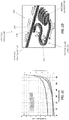
- FIGS. 1A-1D illustrate an optical phased array 100 formed using a CMOS integration process.
- the optical phased array 100 includes 4,096 unit cells (pixels) 130 arranged in 64 pixel ⁇ 64 pixel grid at a pitch of about ⁇ 0 /2, where ⁇ 0 is the wavelength of the beam(s) emitted by the optical phased array 100.
- An optical fiber 102 couples light from a laser or other coherent light source (not shown) into a column bus waveguide 110, which in turn evanescently couples light into 64 row bus waveguides 120-1 through 120-64 (collectively, row bus waveguides 120).
- Each row bus waveguide 120 in turn evanescently couples light into 64 pixels 130, which emit light to form a predetermined far-field emission pattern.
- each row bus waveguide 120 obtains the same amount of power as described in greater detail below.
- the optical power in each row bus waveguide 120 is then similarly divided among the 64 pixels 130 coupled to that row bus waveguide 120 so that all 4,096 optical nanoantennas in the optical phased array 100 are uniformly excited. Because each pixel 130 receives an equal portion of the optical power provided by the optical fiber 102, differences in the relative phases of the beams emitted by the pixels 130 determine the optical phased array's far-field emission pattern.
- the optical power coupled into and/or out of each pixel 130 may be weighted, attenuated, or amplified to produce a pixel-by-pixel variation in the emitted power to produce a particular far-field radiation pattern.
- the pixel pitch is less than half of the free-space wavelength, ⁇ 0 , of the optical emission in both the x and y directions. Because the pixel pitch is less than ⁇ 0 /2, then the optical phased array 100 can produce a unique interference pattern in the far field without high-order radiation lobes. For pixel pitches greater than ⁇ 0 /2, the optical phased array 100 may produce (possibly undesired) high-order interference patterns in the far field in addition to the desired far-field radiation pattern. In other words, the optical phased array 100 may produce aliased versions of the desired pattern in the far field.
- the amplitudes of the pixels' respective emissions affect the far-field radiation pattern. Undesired variations in these amplitudes may corrupt or otherwise degrade the optical phased array's far-field radiation pattern. Preventing undesired amplitude variations often becomes more challenging (and more important) in larger arrays.
- the power feeding network should deliver optical power reliably and precisely to each antenna element.
- FIG. 1B illustrates the optical phased array's power feeding network-the column bus waveguide 110 and the row bus waveguides 120-in greater detail.
- the column bus waveguide 110 and row bus waveguides 120 may be formed of silicon waveguides (e.g., silicon-on-insulator waveguides) as understood in the art of CMOS processing and CMOS electronics.
- the column bus waveguide 110 is butt-coupled to the optical fiber 102, which launches an optical beam into a single transverse mode supported by the column bus waveguide 110.
- the optical beam propagates along the column bus waveguide 110 through a series of column-to-row directional couplers 140-1 through 140-64 (collectively, directional couplers 140), each of which couples a corresponding portion of the optical beam into a corresponding row bus waveguide 120.
- the directional couplers 140-1 through 140-64 shown in FIG. 1B are four-port, passive devices formed by respective column coupling regions 112-1 through 112-64 (collectively, coupling regions 112) of the column bus waveguide 110.
- the column coupling region 112 runs parallel to and spaced apart from a row coupling region 122-1 through 122-64 (collectively, coupling regions 122) in the corresponding row bus waveguide 120-1 through 120-64.
- the desired coupling ratios (and coupler lengths) can be obtained through a three-dimensional finite-difference time-domain simulation or any other suitable technique. For the 64 pixel ⁇ 64 pixel optical phased array 100 shown in FIG.
- the power distribution across the optical phased array may be nonuniform.
- the power distribution may have a Gaussian or exponentially decaying envelope to provide a Gaussian or Lorentzian shape to the beams emitted by the optical phase array.
- the directional couplers' coupling ratios can be changed by varying the separation distance between the coupling regions 112 and 122 instead of or in addition to varying the coupler length. The coupling efficiency tends to be less sensitive to variations in coupler length than to variations in the separation distance, however, so directional couplers 140 with varying lengths tend to have looser fabrication tolerances than directional couplers with varying separation distances.
- each directional coupler may include an interferometer, such as a Mach-Zehnder modulator or ring resonator, with an input port coupled to the column bus waveguide, a first output port coupled to the column bus waveguide, and a second output port coupled to the row bus waveguide.
- Tuning the interferometer with an electric field (e.g., via electrodes) or magnetic field (e.g., via electromagnets) changes its coupling ratio, allowing adjustment of the optical power coupled from the column bus waveguide into the row bus waveguide.
- one or more of the row bus waveguides may include a variable optical attenuators at or near its optical connection with the column bus waveguide. Actuating the variable optical attenuator reduces the optical power propagating through the corresponding row bus waveguide.
- the column bus waveguide may also include one or more variable optical attenuators, e.g., distributed between the successive directional couplers. Actuating a variable optical attenuator in the column bus waveguide reduces the optical power available for coupling into the row bus waveguide(s) downstream from the variable optical attenuator.
- FIG. 1C is a plot that illustrates the performance of the power feeding network in the optical phased array 100 of FIGS. 1A-1C . It shows the coupler length (left axis) and coupling efficiency (right axis) versus row/column index for the directional couplers that connect the column bus waveguide 110 to the row bus waveguides 120 and for the row-to-pixel directional couplers (described below with respect to FIG. 1D ) that connect the row bus waveguides 120 to the pixels 130 in the optical phased array 100 of FIG. 1A .
- FIG. 1D shows a pixel 130 in the optical phased array 100 of FIG. 1A in greater detail.
- the pixel 130 includes a pixel waveguide 132 that is formed using the same CMOS process used to form the column bus waveguide 110 and the row bus waveguides 120.
- all of these waveguides may be formed of the same semiconductor material, such as silicon or silicon nitridge, on a layer of dielectric cladding, such as silicon oxide (SiO x ).
- these waveguides may guide light at visible wavelengths or infrared wavelengths.
- the waveguides may be about 220 nm tall and about 400 nm wide.
- the pixel waveguide 132 is evanescently coupled to a corresponding row bus waveguide 120 via a row-to-pixel directional coupler 150.
- the row-to-pixel directional coupler 150 is formed by a coupling region 124 in the row bus waveguide 120 that runs parallel to and spaced apart from a coupling region 134 in the pixel waveguide 132.
- the row-to-pixel directional coupler 150 has a length (and/or width) that is selected to couple a predetermined percentage of the optical power from the row bus waveguide 120 into the pixel waveguide 132.
- the row-to-pixel directional coupler 150 may include an active device that can be used to vary the amount of optical power coupled into (and out of) the pixel 130.
- the pixel waveguide 132 couples light into an antenna element 138 (also known as a nanoantenna, nanophotonic antenna, or element) via an S-shaped static optical delay line 136.
- the static optical delay line 136 is formed of a section of the pixel waveguide 132 whose optical path length is selected to shift the phase of wave propagating through the pixel waveguide 132 by a predetermined amount ⁇ mn .
- the static optical delay line 136 includes two sections, each of which induces a phase shift ⁇ mn /2 , where m and n are the pixel's row and column indices, for a total phase shift ⁇ mn .
- the pixel may include an optical delay line more or fewer segments, each of which induces an appropriately selected phase shift (e.g., ⁇ mn /4 and 3 ⁇ mn /4, ⁇ mn /3 and 2 ⁇ mn /3 , etc.).
- an appropriately selected phase shift e.g., ⁇ mn /4 and 3 ⁇ mn /4, ⁇ mn /3 and 2 ⁇ mn /3 , etc.
- the delay line design makes the position of the antenna element 138 independent of the phase delay ⁇ mn , so that all of the antenna elements 138 can be placed on a periodic grid.
- the varied coupler length slightly affects the phases of the transmitted light and the coupled-out light. This effect can be accounted for when calculating the phase shift ⁇ mn for each pixel 130.
- the antenna element 138 shown in FIG. 1D is a dielectric grating formed in the same plane as the column bus waveguide 110, the row bus waveguides 120, and the pixel waveguide 132.
- the grating diffracts light up and down, out of the plane of the waveguides and the grating. Because the grating has a relatively small number (e.g., 5) of rulings, its may have a diffraction bandwidth with a full-width half-maximum of hundreds of nanometers (e.g., 100 nm, 200 nm, etc.). In some cases, the grating may be blazed to diffract more light up than down (or vice versa).
- the grating period may be slightly detuned from resonant emission to avoid reflecting radiation back into the pixel waveguide 132, where it could be produce undesired interference. This detuning may shift the optical axis of the emitted beam away from the surface normal of the grating.
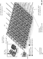
- FIGS. 2A and 2B illustrate an 8 ⁇ 8 actively tunable optical phased array 200 and a unit cell (pixel) 230, respectively.
- the active phased array 200 shown in FIG. 2A includes a source of optical radiation-in this case, an optical fiber 202 coupled to a laser (not shown)-that launches an optical beam with a free-space wavelength ⁇ 0 into a single-mode column bus waveguide 210.
- Evanescent directional couplers 240-1 through 240-8 (collectively, directional couplers 240) like those described with respect to FIG. 1B couple light from the column bus waveguide 210 into eight different row bus waveguides 220-1 through 220-8 (collectively, row bus waveguides 220).
- the directional couplers' coupling efficiencies may vary so as to ensure that each row bus waveguide receives a predetermined amount (e.g., an equal amount) of optical power from the column bus waveguide 210.
- Each row bus waveguide 220 guides an optical beam from the corresponding directional coupler 240 to eight unit cells (pixels) 230, each of which can be on the order of ⁇ 0 (e.g., about 9 ⁇ m ⁇ 9 ⁇ m).
- directional couplers 250 evanescently couple light from the row bus waveguide 220 to corresponding unit cells 230, each of which includes a silicon waveguide 232 that couples light into a grating-based antenna element 238.
- This antenna element 238 emits the light with a desired amplitude and phase to form a pattern in the far field of the active optical phased array 200.
- the active optical phased array 200 includes a pixel addressing matrix that can be used to independently vary the phases of the beams emitted by the pixels 230.
- the pixel addressing matrix is formed of column control wires 260-1 through 260-8 (collectively, column control wires 260) and row control wires 262-1 through 262-8 (collectively, row control wires 262).
- the column control wires 260 and row control wires 262 are disposed in parallel planes above the pixels 230; in other examples, the control wires may be routed in planes below the pixels 230 instead.
- each column control wire 260 runs above a corresponding column of pixels 230 and is electrically coupled to a copper-silicon electrical contact 264 in each of the pixels 230 in the column.
- each row control 262 runs above a corresponding row of pixels 230 and is electrically coupled to a copper-silicon electrical contact 268 in each pixel 230 in the row.
- the electrical contacts 264 and 268 in each pixel 230 are electrically coupled to a corresponding integrated heater 266 formed by doping a portion of the silicon waveguide 232.
- Each heater 266 may have a resistance of about 2.5 k ⁇ , including the resistance of the contacts 264 and 268.
- Applying a voltage to a particular column control wire 260-m and a particular row control wire 262- n causes a change in the electrical potential across the integrated heater 266 in the pixel 230- mn at the intersection of the column control wire 260-m and the row control wire 262- n.
- This potential change causes the heater 266 to change temperature (get hotter or colder), leading to a corresponding change in the optical path length of the doped portion of the silicon waveguide 232 via the thermo-optic effect. And this change in optical path length induces a corresponding phase shift in the optical beam propagating through the waveguide 232 to the antenna element 238.
- the heater 266 may operate with a thermal efficiency of about 8.5 mW per 7° of phase shift.
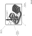
- FIGS. 3A and 3B illustrate an active optical phased array 300 that uses liquid-based tuning instead of (or in addition) to integrated heaters for varying the phases of the beams emitted by the pixels.
- an optical fiber 302 coupled to a laser launches an optical beam with a free-space wavelength ⁇ 0 into a single-mode column bus waveguide 310.
- Evanescent directional couplers 340 couple light from the column bus waveguide 310 into row bus waveguides 320 with coupling efficiencies selected to ensure that each row bus waveguide 320 receives a predetermined amount (e.g., an equal amount) of optical power from the column bus waveguide 310.
- Each row bus waveguide 320 guides an optical beam from the corresponding directional coupler 340 to a corresponding set of unit cells (pixels) 330, each of which can be on the order of ⁇ 0 (e.g., about 9 ⁇ m ⁇ 9 ⁇ m).
- Directional couplers 350 evanescently couple light from the row bus waveguide 320 to corresponding unit cells 330, each of which includes a silicon waveguide 332 that couples light into a grating-based antenna element 338 as shown in FIG. 3B .
- This antenna element 338 emits the light with a desired amplitude and phase to form a pattern in the far field of the active optical phased array 300.
- the active optical phased array 300 shown in FIG. 3A includes column control wires 360 and row control wires 362 in parallel planes above the plane of the pixels 330. These column control wires 360 and row control wires 362 are connected to electrical contacts 374 and 376 in the individual pixels 330 as shown in FIG. 3B , much like the control wires shown in FIGS. 2A and 2B .
- the active optical phased array 300 illustrated in FIGS. 3A and 3B also includes an array of fluid reservoirs 379 disposed above the unit cells 330.
- the fluid comprises electro-active liquid crystal material 378 that is transparent at the phased array's emission wavelength ⁇ 0 .
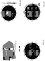
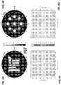
- FIG. 4A shows a near-field emission pattern, simulated using three-dimensional finite-difference time-domain methods, from a grating antenna element that emits 51% of the optical power upwards and 30% downwards at a wavelength of 1.55 ⁇ m.
- the emission is not vertical (normal to the surface) because the grating period is slightly detuned from the period of a second-order grating that would emit vertically. This detuning suppresses resonant back-reflections that might otherwise interfere with the light propagating in the phased array.
- the emission from the nanoantenna is also broadband, with a full-width bandwidth extending across hundreds of nanometers (e.g., more than 100 nm) in wavelength.
- FIGS. 4B-4D show simulated far-field patterns of the optical nanoantenna shown in FIG. 4A (FIG. 4B ) and arrays of the optical nanoantenna shown in FIG. 4A calculated using the near-to-far-field transformation.
- These far-field patterns appear as projections of the far-field hemisphere to the equatorial plane in a polar coordinate system. They are viewed from the zenith of the far-field hemisphere, where ⁇ and ⁇ are the far-field azimuth angle and polar angle, respectively. In each case, the projected pattern is visible mainly in the vicinity of the zenith due to the directional emission of the optical nanoantenna.
- FIGS. 4C and 4D show simulations of the radiation pattern of a 64 ⁇ 64 nanophotonic phased array designed to generate the MIT logo in the far field.
- This radiation pattern is a superposition of the far field of the system's array factor (as shown in the background) and that of the nanoantenna (in FIG. 4A ).
- the circle in the center of FIG. 4C indicates the viewable region in a microscope lens (e.g., with a numerical aperture of 0.4) as also shown in FIGS. 10E and 10F (described below).
- FIG. 4D shows a close-up view of the viewable region of the far field displaying the MIT logo.
- the inset on the lower right shows the MIT logo pattern.
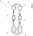
- FIG. 5 is a block diagram that illustrates an efficient iterative process 500 for finding the optical phase v mn to generate a given radiation pattern F a ( ⁇ , ⁇ ) using the Gerchberg-Saxton algorithm.
- an approximated array factor F a k ⁇ , ⁇ which includes the desired amplitude
- the far-field trial phase ⁇ k ( ⁇ , ⁇ ) can be chosen arbitrarily since it does not necessarily affect the final far-field radiation image (block 520).
- the pixel amplitude of w k mn is then set to 1, without changing the phase, to keep the amplitude of the nanoantennas' emission uniform across the array. Therefore the updated array factor F a * ⁇ , ⁇ is obtained through a Fourier transform (block 540) whose phase ⁇ *k ( ⁇ , ⁇ ) is passed to the (k + 1) th iteration as the new trial phase ⁇ k+1 ( ⁇ , ⁇ ) (block 550).
- the final array factor F a * k ⁇ , ⁇ generated by the phase exp ( i ⁇ mn ) converges to the desired pattern
- FIGS. 6A-6D show simulations of a 64 ⁇ 64 nanophotonic phased array with a pixel pitch of ⁇ 0 /2 that used to produce a pattern in the far field with phases generated using antenna synthesis.
- FIG. 6A shows the "MIT" logo as projected in the far field
- FIG. 6C shows the corresponding phase distribution across the face of the array.
- FIG. 6B shows multiple beams with different angles in the far field, with the corresponding phase distribution shown in FIG. 6D .
- projecting multiple beams at different angles can be useful in optical free space communications.
- Equation (2) The actual resulting array factor pattern in the presence of phase noise is again given by Equation (2), with the phase where F a ac ⁇ , ⁇ stands for the actual array factor pattern with noise, F a id ⁇ , ⁇ is the ideal array factor pattern, and ⁇ is the convolution operator.
- the expectation value (denoted by the angle brackets) is used here, meaning that the average value is taken for the stochastic variables and functions.
- SNR signal-to-noise ratio
- phased array exhibits high tolerance to phase errors, which relaxes accuracy requirements on fabrication, and suggests that a large-scale nanophotonic phased array can be produced reliably and function properly.
- this high error tolerance does not depend on the scale of array.
- statistical considerations imply that the analysis above applies more precisely to an array with a larger number of nanoantennas. As a result, the nanophotonic phased array beyond 64 ⁇ 64 to millions of pixels.
- Nanophotonic phased arrays were fabricated in a 300-mm CMOS foundry with a 65-nm technology node, using silicon-on-insulator wafers with a 0.22 ⁇ m top silicon layer and 2 ⁇ m buried oxide.
- a timed partial silicon etch (0.11 ⁇ m) was first performed to make the partly etched grating groove.
- a full silicon etch was then applied to form the waveguides and grating nanoantennas.
- Subsequent n and n+ dopings were implanted for active arrays, followed by standard silicidation to make copper-silicon contacts. The contacts were connected to on-chip probing pads by two metal layers for thermo-optic tuning.
- SiO 2 with a total thickness of 3.6 ⁇ m was used to cover the devices, with a final polishing step to make the surface planar to avoid additional phase errors due to surface corrugation.
- FIG. 9A is a close up of the silicon dielectric nanoantenna in the pixel of FIG. 8B .
- the nanoantenna is used as an emitter in each pixel for direct integration with CMOS process.
- Lighter regions represent silicon with a height of 220 nm
- darker regions represent the buried oxide (BOX) layer underneath the silicon
- the moderately shaded region represents partially etched silicon with a height of 110 nm.
- the nanoantenna measures 3.0 ⁇ m ⁇ 2.8 ⁇ m and includes five grating etches.
- the first grating etch is halfway through the 220 nm-thick silicon layer to create an up-down asymmetry in order to emit more power up and out of the plane of the phased array.
- FIG. 10A is a diagram of an imaging system 1000 used to observe the near field and far field of the nanophotonic phased array 1010 shown in FIGS. 8A, 8B , and 9A emitting light at a wavelength of 1.55 ⁇ m.
- a first lens 1020 alone (numerical aperture 0.40) was used to obtain a near-field (NF) image with an infrared charge-coupled device (IRCCD) 1040, as shown by the outer rays.
- NF near-field
- ITCD infrared charge-coupled device
- the far-field (FF) image was taken by moving the first lens 1020 down (to position 1020') so as to form the far-field image in its back-focal plane (Fourier plane) and inserting a second lens 1030 to project the far-field image onto the IRCCD 1040, as shown by the inner rays.
- FIG. 10E shows the measured far-field radiation pattern of the fabricated 64 ⁇ 64 nanophotonic phased array.
- the image reveals that the desired radiation pattern (in this case, the MIT logo) appears in the far field.
- the far-field image is clamped by the finite numerical aperture (0.4) of lens 1020 in FIG. 10A .
- This is also predicted by simulations, as shown by the circles in FIGS. 4C and 4D , which show that emission within a small divergence angle from vertical (surface normal to the nanophotonic phased array chip) can be captured.
- the intensity noise in the background of the far-field image comes from the light scattering caused by fiber-to-waveguide coupling.
- the scattered light is also responsible for the concentric fringes in the background, through the interference of the scattered light between the top and bottom surfaces of the silicon-on-insulator wafer.
- This noise can be reduced by placing the fiber-waveguide coupler farther from the NPA system to reduce the light scattering captured by the imaging column, and a much cleaner far-field radiation pattern would be expected.
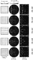
- FIGS. 11A-11E show good agreement between simulation and experiment, which confirms the robustness of the nanophotonic phased array as well as the accuracy of the fabrication and active thermo-optic phase tuning.
- the active NPA structure can be extended to larger phased arrays (for example 64 ⁇ 64, as discussed above) with independent electrical control of each pixel with the aid of fully CMOS-controlled circuitry to access all of the pixels electrically, to project dynamic patterns in the far field with applications including but not limited t ocommunications, three-dimensional holographic displays, laser detection and ranging (LADAR), biomedical imaging, and interferometry.
- LADAR laser detection and ranging
- inventive embodiments are presented by way of example only and that, within the scope of the appended claims and equivalents thereto, inventive embodiments may be practiced otherwise than as specifically described and claimed.
- inventive embodiments of the present disclosure are directed to each individual feature, system, article, material, kit, and/or method described herein.
- embodiments of designing and making the coupling structures and diffractive optical elements disclosed herein may be implemented using hardware, software or a combination thereof.
- the software code can be executed on any suitable processor or collection of processors, whether provided in a single computer or distributed among multiple computers.
- a computer may be embodied in any of a number of forms, such as a rack-mounted computer, a desktop computer, a laptop computer, or a tablet computer. Additionally, a computer may be embedded in a device not generally regarded as a computer but with suitable processing capabilities, including a Personal Digital Assistant (PDA), a smart phone or any other suitable portable or fixed electronic device.
- PDA Personal Digital Assistant
- Such computers may be interconnected by one or more networks in any suitable form, including a local area network or a wide area network, such as an enterprise network, and intelligent network (IN) or the Internet.
- networks may be based on any suitable technology and may operate according to any suitable protocol and may include wireless networks, wired networks or fiber optic networks.
- Computer-executable instructions may be in many forms, such as program modules, executed by one or more computers or other devices.
- program modules include routines, programs, objects, components, data structures, etc. that perform particular tasks or implement particular abstract data types.
- functionality of the program modules may be combined or distributed as desired in various embodiments.
- data structures may be stored in computer-readable media in any suitable form.
- data structures may be shown to have fields that are related through location in the data structure. Such relationships may likewise be achieved by assigning storage for the fields with locations in a computer-readable medium that convey relationship between the fields.
- any suitable mechanism may be used to establish a relationship between information in fields of a data structure, including through the use of pointers, tags or other mechanisms that establish relationship between data elements.
- At least one of A and B can refer, in one embodiment, to at least one, optionally including more than one, A, with no B present (and optionally including elements other than B); in another embodiment, to at least one, optionally including more than one, B, with no A present (and optionally including elements other than A); in yet another embodiment, to at least one, optionally including more than one, A, and at least one, optionally including more than one, B (and optionally including other elements); etc.
Landscapes
- Physics & Mathematics (AREA)
- General Physics & Mathematics (AREA)
- Optics & Photonics (AREA)
- Nonlinear Science (AREA)
- Engineering & Computer Science (AREA)
- Microelectronics & Electronic Packaging (AREA)
- Mathematical Physics (AREA)
- Variable-Direction Aerials And Aerial Arrays (AREA)
- Optical Modulation, Optical Deflection, Nonlinear Optics, Optical Demodulation, Optical Logic Elements (AREA)
- Liquid Crystal (AREA)
- Optical Couplings Of Light Guides (AREA)
- Optical Integrated Circuits (AREA)
Claims (15)
- Optisches Phasenarray zum Bilden eines Fernfeld-Strahlungsdiagramms von einem kohärenten optischen Strahl mit einer Freiraumwellenlänge λ0, wobei das optische Phasenarray Folgendes umfasst:ein Substrat;wenigstens einen auf dem Substrat ausgebildeten Wellenleiter (110, 120) zum Leiten des kohärenten optischen Strahls; undmehrere auf dem Substrat ausgebildete Antennenelemente (138), evaneszent gekoppelt mit dem wenigstens einen Wellenleiter durch jeweilige Pixelwellenleiter (132, 232), die jeweilige direktionale Koppler mit dem wenigstens einen Wellenleiter bilden, zum Emittieren von jeweiligen Teilen des kohärenten optischen Strahls in einem Winkel mit Bezug auf das Substrat, um das Fernfeld-Strahlungsdiagramm zu bilden, wobei die direktionalen Koppler einen ersten direktionalen Koppler mit einer ersten vorbestimmten Kopplungseffizienz und einen zweiten direktionalen Koppler mit einer zweiten vorbestimmten Kopplungseffizienz umfassen, die sich von der ersten vorbestimmten Kopplungseffizienz unterscheidet.
- Optisches Phasenarray nach Anspruch 1, wobei der wenigstens eine Wellenleiter Folgendes umfasst:einen Spaltenwellenleiter (110) zum Leiten des kohärenten optischen Strahls in einer ersten Richtung; undwenigstens einen mit dem Spaltenwellenleiter evaneszent gekoppelten Reihenwellenleiter (120) zum Leiten eines ersten Teils des kohärenten optischen Strahls zu wenigstens einem Antennenelement in den mehreren Antennenelementen.
- Optisches Phasenarray nach Anspruch 2, wobei der wenigstens eine Reihenwellenleiter Folgendes umfasst:einen mit dem Spaltenwellenleiter über den ersten direktionalen Koppler evaneszent gekoppelten ersten Reihenwellenleiter zum Leiten des ersten Teils des kohärenten optischen Strahls mit einer ersten Amplitude; undeinen mit dem Spaltenwellenleiter über den zweiten direktionalen Koppler evaneszent gekoppelten zweiten Reihenwellenleiter zum Leiten eines zweiten Teils des kohärenten optischen Strahls mit einer zweiten Amplitude.
- Optisches Phasenarray nach Anspruch 3, wobei die erste vorbestimmte Kopplungseffizienz und die zweite vorbestimmte Kopplungseffizienz so gewählt sind, dass die erste Amplitude etwa gleich der zweiten Amplitude ist.
- Optisches Phasenarray nach Anspruch 1, wobei der wenigstens eine Wellenleiter (110, 120) über einen komplementären Metalloxidhalbleiter-(CMOS)-Prozess gebildet ist.
- Optisches Phasenarray nach Anspruch 1, wobei Antennenelemente (138) in den mehreren Antennenelementen mit einer Teilung von gleich einem ganzzahligen Vielfachen von λ0/2 beabstandet sind.
- Optisches Phasenarray nach Anspruch 1, wobei Antennenelemente (138) in den mehreren Antennenelementen mit einer Teilung von gleich oder kleiner als etwa λ0/2 beabstandet sind.
- Optisches Phasenarray nach Anspruch 1, wobei die jeweiligen Teile des von den mehreren Antennenelementen emittierten kohärenten optischen Strahls etwa die gleiche Amplitude haben.
- Optisches Phasenarray nach Anspruch 1, das ferner Folgendes umfasst:
wenigstens eine variable optische Verzögerungsleitung (232) in optischer Kommunikation mit wenigstens einem Antennenelement in den mehreren Antennenelementen zum Verschieben einer Phase eines entsprechenden Teils des kohärenten optischen Strahls, um eine Amplitudenverteilung des Fernfeld-Strahlungsdiagramms zu variieren und/oder um Phasenfehler in dem wenigstens einen Wellenleiter zu kompensieren. - Optisches Phasenarray nach Anspruch 9, das ferner Folgendes umfasst:
wenigstens eine Heizung (266) in thermischer Kommunikation mit der wenigstens einen variablen optischen Verzögerungsleitung zum Heizen wenigstens eines Teils der wenigstens einen variablen optischen Verzögerungsleitung, um die Phasenverschiebung zu ändern, die dem entsprechenden Teil des kohärenten optischen Strahls durch die wenigstens eine variable optische Verzögerungsleitung vermittelt wird. - Optisches Phasenarray nach Anspruch 10, wobei die wenigstens eine Heizung eine in einem dotierten Halbleiter ausgebildete Widerstandsheizung umfasst.
- Optisches Phasenarray nach Anspruch 10, das ferner Folgendes umfasst:
eine Steuerung, die operativ mit der wenigstens einen Heizung gekoppelt ist, zum Regeln einer Temperatur der wenigstens einen Heizung, um das Fernfeld-Strahlungsdiagramm über eine Änderung der Phasenverschiebung zu variieren, die dem entsprechenden Teil des kohärenten optischen Strahls durch die wenigstens eine variable optische Verzögerungsleitung vermittelt wird. - Optisches Phasenarray nach Anspruch 9, das ferner Folgendes beinhaltet:
ein Gitter in optischer Kommunikation mit der wenigstens einen variablen optischen Verzögerungsleitung zum Beugen wenigstens eines Teils des entsprechenden Teils des kohärenten optischen Strahls, um das Fernfeld-Strahlungsdiagramm zu bilden. - Optisches Phasenarray nach Anspruch 13, wobei das Gitter eine Vollbreiten-Halbmaximum-Beugungsbandbreite von wenigstens etwa 100 nm hat.
- Optisches Phasenarray nach Anspruch 13, wobei das Gitter zum Unterdrücken von resonanter Rückreflexion des entsprechenden jeweiligen Teils des kohärenten optischen Strahls konfiguriert ist.
Priority Applications (1)
| Application Number | Priority Date | Filing Date | Title |
|---|---|---|---|
| EP18167812.9A EP3388892A1 (de) | 2013-01-08 | 2014-01-07 | Optische phasenarrays |
Applications Claiming Priority (2)
| Application Number | Priority Date | Filing Date | Title |
|---|---|---|---|
| US201361749967P | 2013-01-08 | 2013-01-08 | |
| PCT/US2014/010450 WO2014110017A1 (en) | 2013-01-08 | 2014-01-07 | Optical phased arrays |
Related Child Applications (2)
| Application Number | Title | Priority Date | Filing Date |
|---|---|---|---|
| EP18167812.9A Division-Into EP3388892A1 (de) | 2013-01-08 | 2014-01-07 | Optische phasenarrays |
| EP18167812.9A Division EP3388892A1 (de) | 2013-01-08 | 2014-01-07 | Optische phasenarrays |
Publications (3)
| Publication Number | Publication Date |
|---|---|
| EP2929382A1 EP2929382A1 (de) | 2015-10-14 |
| EP2929382A4 EP2929382A4 (de) | 2016-06-08 |
| EP2929382B1 true EP2929382B1 (de) | 2018-05-30 |
Family
ID=51060755
Family Applications (2)
| Application Number | Title | Priority Date | Filing Date |
|---|---|---|---|
| EP18167812.9A Withdrawn EP3388892A1 (de) | 2013-01-08 | 2014-01-07 | Optische phasenarrays |
| EP14737546.3A Active EP2929382B1 (de) | 2013-01-08 | 2014-01-07 | Optische phasenarrays |
Family Applications Before (1)
| Application Number | Title | Priority Date | Filing Date |
|---|---|---|---|
| EP18167812.9A Withdrawn EP3388892A1 (de) | 2013-01-08 | 2014-01-07 | Optische phasenarrays |
Country Status (7)
| Country | Link |
|---|---|
| US (1) | US8988754B2 (de) |
| EP (2) | EP3388892A1 (de) |
| JP (2) | JP6363619B2 (de) |
| KR (3) | KR102181537B1 (de) |
| CN (2) | CN111522098A (de) |
| CA (1) | CA2897036A1 (de) |
| WO (1) | WO2014110017A1 (de) |
Families Citing this family (182)
| Publication number | Priority date | Publication date | Assignee | Title |
|---|---|---|---|---|
| CN103378921B (zh) * | 2012-04-17 | 2016-08-03 | 华为技术有限公司 | 信号解调方法和装置 |
| EP3388892A1 (de) * | 2013-01-08 | 2018-10-17 | Massachusetts Institute Of Technology | Optische phasenarrays |
| US9476981B2 (en) | 2013-01-08 | 2016-10-25 | Massachusetts Institute Of Technology | Optical phased arrays |
| US10132928B2 (en) | 2013-05-09 | 2018-11-20 | Quanergy Systems, Inc. | Solid state optical phased array lidar and method of using same |
| US10126412B2 (en) * | 2013-08-19 | 2018-11-13 | Quanergy Systems, Inc. | Optical phased array lidar system and method of using same |
| US10203399B2 (en) | 2013-11-12 | 2019-02-12 | Big Sky Financial Corporation | Methods and apparatus for array based LiDAR systems with reduced interference |
| US9104086B1 (en) * | 2014-02-24 | 2015-08-11 | Sandia Corporation | Method and apparatus of wide-angle optical beamsteering from a nanoantenna phased array |
| WO2015135003A2 (en) * | 2014-03-04 | 2015-09-11 | California Institute Of Technology | Directional optical receiver |
| US9360554B2 (en) | 2014-04-11 | 2016-06-07 | Facet Technology Corp. | Methods and apparatus for object detection and identification in a multiple detector lidar array |
| US9753351B2 (en) | 2014-06-30 | 2017-09-05 | Quanergy Systems, Inc. | Planar beam forming and steering optical phased array chip and method of using same |
| US9869753B2 (en) * | 2014-08-15 | 2018-01-16 | Quanergy Systems, Inc. | Three-dimensional-mapping two-dimensional-scanning lidar based on one-dimensional-steering optical phased arrays and method of using same |
| US10036803B2 (en) | 2014-10-20 | 2018-07-31 | Quanergy Systems, Inc. | Three-dimensional lidar sensor based on two-dimensional scanning of one-dimensional optical emitter and method of using same |
| US10274575B2 (en) | 2015-02-25 | 2019-04-30 | The Charles Stark Draper Laboratory, Inc. | Zero optical path difference phased array |
| US10036801B2 (en) | 2015-03-05 | 2018-07-31 | Big Sky Financial Corporation | Methods and apparatus for increased precision and improved range in a multiple detector LiDAR array |
| CN107567592B (zh) | 2015-04-07 | 2021-07-16 | 闪光股份有限公司 | 小型激光雷达系统 |
| US10359630B2 (en) * | 2015-06-30 | 2019-07-23 | Massachusetts Institute Of Technology | Display apparatus comprising first and second optical phased arrays and method for augmented reality |
| CN104933966B (zh) * | 2015-07-23 | 2018-01-26 | 京东方科技集团股份有限公司 | 一种显示面板及其驱动方法、显示装置 |
| KR102422784B1 (ko) * | 2015-08-03 | 2022-07-19 | 엘지이노텍 주식회사 | 광파 탐지 및 거리 측정 장치 |
| US9778421B2 (en) * | 2015-10-14 | 2017-10-03 | Nistica, Inc. | Large scale optical switch using asymmetric 1×2 elements |
| KR101720434B1 (ko) * | 2015-11-10 | 2017-03-28 | 한국과학기술원 | 광 위상배열 안테나 |
| KR101718240B1 (ko) * | 2015-11-16 | 2017-03-21 | 한국과학기술원 | 초소형 광 위상배열 안테나 |
| KR101872077B1 (ko) * | 2015-11-17 | 2018-06-28 | 한국과학기술원 | 광 위상 배열 안테나에 적용을 위한 격자 구조를 이용한 나노포토닉 발산기 |
| WO2017086524A1 (ko) * | 2015-11-17 | 2017-05-26 | 한국과학기술원 | 광 위상 배열 안테나에 적용을 위한 격자 구조를 이용한 나노포토닉 발산기 |
| CN108292053B (zh) * | 2015-11-17 | 2022-03-15 | 韩国高等科学技术学院 | 具有适用于光相位排列天线的可调制光栅结构的纳米光学辐射器 |
| KR101882062B1 (ko) * | 2015-11-17 | 2018-07-25 | 한국과학기술원 | 광 위상 배열 안테나에 적용을 위한 변조 가능한 격자 구조를 갖는 나노포토닉 발산기 |
| CN105449377A (zh) * | 2015-12-16 | 2016-03-30 | 天津大学 | 一种基于半导体工艺的巨量太赫兹天线阵 |
| DE102015225863A1 (de) * | 2015-12-18 | 2017-06-22 | Robert Bosch Gmbh | Optische phasengesteuerte Anordnung und LiDAR System |
| US9866816B2 (en) | 2016-03-03 | 2018-01-09 | 4D Intellectual Properties, Llc | Methods and apparatus for an active pulsed 4D camera for image acquisition and analysis |
| JP6711025B2 (ja) * | 2016-03-03 | 2020-06-17 | 株式会社豊田中央研究所 | グレーティングカプラ、グレーティングカプラアレイ、結像光学系、光スキャナ、及びレーザレーダ装置 |
| US9927559B2 (en) * | 2016-03-25 | 2018-03-27 | Imec Vzw | Wavelength-controlled directivity of all-dielectric optical nano-antennas |
| JP2017187649A (ja) * | 2016-04-06 | 2017-10-12 | 株式会社豊田中央研究所 | 光フェーズドアレイ、及び光アンテナ |
| KR101836613B1 (ko) * | 2016-04-08 | 2018-03-09 | 한국과학기술원 | 광파가 공간으로 방사되는 방사각을 조절하는 광 발산기 |
| KR101837266B1 (ko) * | 2016-04-08 | 2018-03-09 | 한국과학기술원 | 광파를 공간으로 방사하는 광 발산기 |
| US10809591B2 (en) | 2016-04-28 | 2020-10-20 | Analog Photonics LLC | Optical phase shifter device |
| CN106027134B (zh) * | 2016-05-20 | 2019-09-20 | 扬州大学 | 一种光子微波相控阵收发系统及其方法 |
| WO2017205442A2 (en) | 2016-05-24 | 2017-11-30 | The Charles Stark Draper Laboratory, Inc. | Optical communications system phase-controlled transmitter and phase-conjugate mirror receiver |
| CA3026091A1 (en) * | 2016-06-02 | 2017-12-07 | Massachusetts Institute Of Technology | Apparatus and methods for optical neural network |
| US10634973B2 (en) * | 2016-08-02 | 2020-04-28 | University Of Southern California | Two-dimensional optical phased array |
| KR102559580B1 (ko) | 2016-08-17 | 2023-07-25 | 삼성전자주식회사 | 광 조향용 OPA, 및 그 OPA를 구비한 LiDAR 시스템 |
| DE102016216711A1 (de) * | 2016-09-05 | 2018-03-08 | Robert Bosch Gmbh | Verfahren zum Ansteuern eines optischen Phasen-Arrays, Verfahren zum Erkennen eines Objekts mittels eines optischen Phasen-Arrays und optisches System |
| JP6520879B2 (ja) | 2016-09-23 | 2019-05-29 | 株式会社豊田中央研究所 | スイッチ式光アンテナ、スイッチ式光アンテナアレイ、および光走査装置 |
| CN108139646B (zh) | 2016-09-29 | 2023-02-28 | 松下知识产权经营株式会社 | 光扫描设备、光接收设备及光检测系统 |
| EP3869266A1 (de) | 2016-09-29 | 2021-08-25 | Panasonic Intellectual Property Management Co., Ltd. | Vorrichtung zur optischen abtastung, lichtaufnahmevorrichtung und system zur optischen detektion |
| US9740079B1 (en) | 2016-10-28 | 2017-08-22 | National Technology & Engineering Solutions Of Sandia, Llc | Integrated optical transceiver with electronically controlled optical beamsteering |
| US11158939B2 (en) * | 2016-11-10 | 2021-10-26 | University Of South Florida | Mm-wave wireless channel control using spatially adaptive antenna arrays |
| CN106410607B (zh) * | 2016-11-17 | 2019-07-26 | 清华大学 | 有源光相控阵光子集成芯片及其制备方法 |
| KR102251273B1 (ko) * | 2016-12-16 | 2021-05-14 | 더 차레스 스타크 드레이퍼 래보레이토리, 인코포레이티드 | 전 고체 광학 송/수신 단말기 |
| US10203452B2 (en) * | 2016-12-30 | 2019-02-12 | Intel Corporation | Wide-angle, aliasing-free beam steering using aperiodic emitter arrays |
| WO2018140075A1 (en) * | 2017-01-24 | 2018-08-02 | Hrl Laboratories, Llc | Dual frequency fmcw lidar and method |
| EP3355077B1 (de) * | 2017-01-25 | 2020-11-11 | Melexis Technologies NV | Lichtdetektions- und -entfernungsmessungssystem |
| WO2018140348A1 (en) | 2017-01-26 | 2018-08-02 | The Charles Stark Draper Laboratory, Inc. | Method and apparatus for light field generation |
| JP2018124402A (ja) * | 2017-01-31 | 2018-08-09 | 日本電信電話株式会社 | 光入出力装置 |
| US10775506B2 (en) | 2017-01-31 | 2020-09-15 | Panasonic Intellectual Property Management Co., Ltd. | Imaging system |
| CN108415205B (zh) * | 2017-02-09 | 2022-11-04 | 松下知识产权经营株式会社 | 光扫描设备、光接收设备以及光检测系统 |
| EP3589974B1 (de) * | 2017-03-01 | 2026-03-04 | Pointcloud Inc. | Modulares dreidimensionales optisches messsystem |
| EP3593206A4 (de) * | 2017-03-06 | 2020-11-25 | Shenzhen Genorivision Technology Co., Ltd. | Lidar-lichtquelle |
| CN108627974A (zh) | 2017-03-15 | 2018-10-09 | 松下知识产权经营株式会社 | 光扫描系统 |
| CN106932866B (zh) * | 2017-03-28 | 2018-12-25 | 中国电子科技集团公司第三十八研究所 | 一种硅基光子器件的自动对光装置及方法 |
| US20210026069A1 (en) * | 2017-03-31 | 2021-01-28 | Universiteit Gent | Integrated near-eye display |
| US10641876B2 (en) | 2017-04-06 | 2020-05-05 | Quanergy Systems, Inc. | Apparatus and method for mitigating LiDAR interference through pulse coding and frequency shifting |
| JP7162266B2 (ja) | 2017-04-20 | 2022-10-28 | パナソニックIpマネジメント株式会社 | 光スキャンデバイス、光受信デバイス、および光検出システム |
| DE112018002172T5 (de) * | 2017-04-25 | 2020-02-20 | Analog Photonics LLC | Gemultiplexter Wellenlängenteilungs-Lidar |
| KR102039889B1 (ko) * | 2017-04-28 | 2019-11-04 | 인하대학교 산학협력단 | 광 조향 장치 |
| US10409074B2 (en) | 2017-05-03 | 2019-09-10 | Microsoft Technology Licensing, Llc | Near-to-eye display with steerable phased arrays |
| CN108803192B (zh) * | 2017-05-04 | 2021-01-01 | 中国科学院化学研究所 | 一种亚波长相干信号补偿装置 |
| US20180321569A1 (en) | 2017-05-04 | 2018-11-08 | The Charles Stark Draper Laboratory, Inc. | Chip scale optical systems |
| EP3635460B1 (de) * | 2017-06-07 | 2021-12-08 | The Charles Stark Draper Laboratory, Inc. | Integrierte mems-schalter zur selektiven kopplung von licht in und aus einem wellenleiter |
| CN108693513A (zh) * | 2017-06-09 | 2018-10-23 | 深圳市涵光半导体有限公司 | 激光雷达及其二维相控阵激光发射单元 |
| US11112491B2 (en) * | 2017-06-29 | 2021-09-07 | Rockley Photonics Limited | Optical scanner and detector |
| KR102407142B1 (ko) * | 2017-06-30 | 2022-06-10 | 삼성전자주식회사 | 빔 스티어링 소자 및 이를 포함하는 전자 장치 |
| CN108693540B (zh) * | 2017-07-11 | 2024-07-02 | 深圳市涵光半导体有限公司 | 相控阵激光雷达 |
| WO2019014596A1 (en) * | 2017-07-14 | 2019-01-17 | Ours Technology, Inc. | SEMICONDUCTOR LIGHT DETECTION AND TELEMETRY SYSTEM BASED ON OPTICAL PHASE CONTROL OPTICAL NETWORK COMPRISING OPTICAL POWER DISTRIBUTION NETWORK |
| KR102434702B1 (ko) | 2017-07-24 | 2022-08-22 | 삼성전자주식회사 | 라이다 시스템 및 이의 구동 방법 |
| US10209509B1 (en) | 2017-07-28 | 2019-02-19 | Panasonic Intellectual Property Management Co., Ltd. | Optical scanning device that includes mirrors and optical waveguide region |
| US11294061B1 (en) * | 2017-08-18 | 2022-04-05 | Acacia Communications, Inc. | LiDAR sensor with orthogonal arrays |
| US10816649B1 (en) | 2017-09-14 | 2020-10-27 | The United States Of America As Represented By The Secretary Of The Air Force | Temporally multiplexed LADAR polarimeter |
| US11428811B2 (en) * | 2017-11-14 | 2022-08-30 | The Charles Stark Draper Laboratory, Inc. | Foveal patterned optical switches for MEMS LiDAR beam steering unit |
| JP7005320B2 (ja) * | 2017-12-05 | 2022-01-21 | 日本放送協会 | 光偏向装置 |
| US10495794B2 (en) * | 2017-12-12 | 2019-12-03 | Huawei Technologies Co., Ltd. | Polarization insensitive optical phased array and associated method |
| CN110446972B (zh) | 2017-12-26 | 2023-11-10 | 松下知识产权经营株式会社 | 光扫描设备、光接收设备及光检测系统 |
| CN110431481B (zh) | 2017-12-28 | 2023-12-08 | 松下知识产权经营株式会社 | 光设备 |
| US10591802B2 (en) * | 2018-01-18 | 2020-03-17 | Litexel Inc. | On-chip optical phased array using a serial grating antenna design |
| KR102474591B1 (ko) | 2018-01-24 | 2022-12-05 | 삼성전자주식회사 | 광 조향 장치 및 이를 포함하는 센서 시스템 |
| US10536223B2 (en) * | 2018-01-24 | 2020-01-14 | Toyota Motor Engineering & Manufacturing North America, Inc. | Phase modulated optical waveguide |
| US10976542B2 (en) | 2018-01-26 | 2021-04-13 | Analog Photonics LLC | Aberration correction of optical phased arrays |
| US10365536B1 (en) | 2018-02-07 | 2019-07-30 | Eagle Technology, Llc | Optical device including a monolithic body of optical material and related methods |
| JP7165734B2 (ja) * | 2018-02-16 | 2022-11-04 | アナログ フォトニクス エルエルシー | 光構造物とこれを較正する方法 |
| US20190260124A1 (en) * | 2018-02-20 | 2019-08-22 | California Institute Of Technology | Perimeter Control Architecture for Phased Array Antennas and Metasurfaces |
| WO2019171806A1 (ja) | 2018-03-09 | 2019-09-12 | パナソニックIpマネジメント株式会社 | 光デバイスおよび光検出システム |
| WO2019187681A1 (ja) * | 2018-03-27 | 2019-10-03 | パナソニックIpマネジメント株式会社 | 光デバイスおよび光検出システム |
| JP7336746B2 (ja) | 2018-03-27 | 2023-09-01 | パナソニックIpマネジメント株式会社 | 光デバイスおよび光検出システム |
| DE102018204715A1 (de) | 2018-03-28 | 2019-10-02 | Robert Bosch Gmbh | Sendevorrichtung zur Aussendung elektro-magnetischer Strahlung |
| WO2019191778A1 (en) * | 2018-03-30 | 2019-10-03 | The Regents Of The University Of California | Photonic beam steering and applications for optical communications |
| CN108398842B (zh) * | 2018-04-18 | 2024-01-05 | 中国科学院西安光学精密机械研究所 | 一种基于串联式光学天线的光学相控阵芯片 |
| JP6513884B1 (ja) * | 2018-04-24 | 2019-05-15 | 株式会社大成テクノロジー | 光フェーズドアレイ、及びこれを用いたlidarセンサ |
| US10884105B2 (en) * | 2018-05-31 | 2021-01-05 | Eagle Technology, Llc | Optical system including an optical body with waveguides aligned along an imaginary curved surface for enhanced beam steering and related methods |
| CN108732681B (zh) * | 2018-06-01 | 2020-09-04 | 航天恒星科技有限公司 | 一种小型化抑制双向辐射的介质光纳米天线 |
| JP7429928B2 (ja) | 2018-09-19 | 2024-02-09 | パナソニックIpマネジメント株式会社 | 光デバイスおよび光検出システム |
| DE102018216775B4 (de) * | 2018-09-28 | 2022-01-20 | Robert Bosch Gmbh | Optisches Phasenarray und Verfahren zum Herstellen eines Phasenarrays |
| CN112470036B (zh) | 2018-10-23 | 2024-10-15 | 松下知识产权经营株式会社 | 光检测系统 |
| GB2578790B (en) | 2018-11-09 | 2023-02-15 | Toshiba Kk | A reference Laser, plurality of first optical components, and a plurality of second optical components integrated laterally on a semiconductor substrate |
| CN111220964B (zh) | 2018-11-27 | 2022-04-15 | 北京万集科技股份有限公司 | 混合材料相控阵激光雷达发射芯片、制作方法及激光雷达 |
| JP2022020871A (ja) | 2018-12-06 | 2022-02-02 | パナソニックIpマネジメント株式会社 | 物体認識装置、物体認識方法、およびプログラム |
| CN112470035B (zh) | 2018-12-06 | 2024-09-24 | 松下知识产权经营株式会社 | 距离信息取得装置、距离信息取得方法及程序 |
| JP6828062B2 (ja) * | 2018-12-12 | 2021-02-10 | 株式会社大成テクノロジー | ライダー装置 |
| CN109491010B (zh) * | 2018-12-14 | 2020-06-09 | 上海交通大学 | 基于光相控阵的硅基集成光学可调延时线 |
| CN109727295B (zh) * | 2018-12-17 | 2021-06-29 | 中国电子产品可靠性与环境试验研究所((工业和信息化部电子第五研究所)(中国赛宝实验室)) | 电磁图像提取方法、装置、计算机设备和存储介质 |
| TW202041847A (zh) * | 2019-01-03 | 2020-11-16 | 美商寬騰矽公司 | 用於傳遞光至光子元件之陣列的光學波導及耦合器 |
| TW202602018A (zh) * | 2019-02-21 | 2026-01-01 | 美商伊雷克托科學工業股份有限公司 | 用於雷射能量的相位陣列波束操縱的系統 |
| US11539186B2 (en) * | 2019-03-06 | 2022-12-27 | Cisco Technology, Inc. | Supermode filtering waveguide emitters |
| CN111751926B (zh) * | 2019-03-28 | 2022-08-26 | 上海新微技术研发中心有限公司 | 用于相控阵发射阵列的波导光栅天线及其形成方法 |
| CN120214771B (zh) | 2019-03-29 | 2025-10-31 | 欧若拉运营公司 | Lidar收发器、lidar系统和lidar芯片 |
| KR102070349B1 (ko) * | 2019-04-17 | 2020-01-28 | 광운대학교 산학협력단 | 리튬나이오베이트-실리콘나이트라이드 기반의 광 위상변조기 및 이를 이용한 광위상 배열안테나 |
| WO2020217645A1 (ja) | 2019-04-25 | 2020-10-29 | パナソニックIpマネジメント株式会社 | 光デバイス、光検出システムおよびその製造方法 |
| WO2020217646A1 (ja) | 2019-04-26 | 2020-10-29 | パナソニックIpマネジメント株式会社 | 光デバイス |
| WO2020226031A1 (ja) | 2019-05-09 | 2020-11-12 | パナソニックIpマネジメント株式会社 | 光デバイスおよび光検出システム |
| US11662643B2 (en) * | 2019-05-09 | 2023-05-30 | The Trustees Of Columbia University In The City Of New York | Chip-scale optical phased array for projecting visible light |
| US11467468B2 (en) * | 2019-05-28 | 2022-10-11 | The Board Of Trustees Of The Leland Stanford Junior University | Dispersion engineered phased array |
| US11539144B2 (en) | 2019-06-03 | 2022-12-27 | Raymond Albert Fillion | Phased array antenna with isotropic and non-isotropic radiating and omnidirectional and non-omnidirectional receiving elements |
| US10838059B2 (en) | 2019-06-03 | 2020-11-17 | Raymond Albert Fillion | Acoustic phased array antenna with isotropic and non-isotropic radiating elements |
| US11411324B2 (en) | 2019-06-03 | 2022-08-09 | Raymond Albert Fillion | Phased array antenna with isotropic and non-isotropic radiating and omnidirectional and non-omnidirectional receiving elements |
| US11588302B2 (en) | 2019-06-21 | 2023-02-21 | Seagate Technology Llc | Optical switches |
| US11143818B2 (en) * | 2019-06-28 | 2021-10-12 | Intel Corporation | Multi-mode interference (MMI) based laser devices for heterogeneous platforms |
| US11906785B2 (en) * | 2019-07-01 | 2024-02-20 | University Of Central Florida Research Foundation, Inc. | Photonic integrated circuit outcoupling array for imaging-based beam steering |
| US11150410B2 (en) | 2019-07-16 | 2021-10-19 | Seagate Technology Llc | Movable optical switching medium |
| CN112449086A (zh) * | 2019-08-30 | 2021-03-05 | Oppo广东移动通信有限公司 | 一种成像装置及成像方法 |
| CN110658661B (zh) * | 2019-08-30 | 2020-10-09 | 北京大学 | 一种用于光学相控阵的相位校准方法及系统 |
| WO2021067911A1 (en) * | 2019-10-04 | 2021-04-08 | University Of Rochester | Optical phased array structure and fabrication techniques |
| KR102223750B1 (ko) | 2019-11-11 | 2021-03-05 | 광주과학기술원 | 광의 위상을 가변할 수 있는 배열 안테나 |
| US11002916B1 (en) | 2019-11-13 | 2021-05-11 | Globalfoundries U.S. Inc. | Non-planar grating couplers for antennas |
| EP3836427B1 (de) | 2019-12-13 | 2025-04-16 | Airbus Defence and Space GmbH | Verfahren, systeme und vorrichtungen für optische freiraumkommunikationen |
| JP7211355B2 (ja) * | 2019-12-25 | 2023-01-24 | 株式会社豊田中央研究所 | 光アンテナ |
| CA3163589A1 (en) | 2020-01-13 | 2021-07-22 | Ours Technology, Llc | Silicon-assisted packaging of high power integrated soa array |
| EP4095598A4 (de) | 2020-01-24 | 2023-07-12 | Panasonic Intellectual Property Management Co., Ltd. | Optische vorrichtung und optisches detektionssystem |
| WO2021247108A2 (en) * | 2020-03-04 | 2021-12-09 | Analog Photonics LLC | Integrated optical phased array electronic control |
| WO2021201966A1 (en) | 2020-04-02 | 2021-10-07 | Massachusetts Institute Of Technology | A chip-scale optical coherence tomography engine |
| CN111487602B (zh) * | 2020-05-26 | 2022-08-16 | 中国电子科技集团公司电子科学研究院 | 光相控阵列、激光雷达及光功率分配方法 |
| US11428785B2 (en) * | 2020-06-12 | 2022-08-30 | Ours Technology, Llc | Lidar pixel with active polarization control |
| US10948600B1 (en) | 2020-06-29 | 2021-03-16 | Aurora Innovation, Inc. | Systems and methods for IQ detection |
| US11280909B2 (en) | 2020-06-29 | 2022-03-22 | Aurora Operations, Inc. | Lidar transmit/receive system |
| US11016197B1 (en) | 2020-06-29 | 2021-05-25 | Aurora Innovation, Inc. | LIDAR system |
| US11366202B2 (en) | 2020-07-01 | 2022-06-21 | Ours Technology, Llc | Semiconductor laser and optical amplifier photonic package |
| US11307483B2 (en) * | 2020-07-02 | 2022-04-19 | Robert Bosch Gmbh | MEMS optical switch with dual cantilever couplers |
| DE102021206988A1 (de) * | 2020-07-02 | 2022-01-05 | Robert Bosch Gesellschaft mit beschränkter Haftung | Mems-schalter für die optische kopplung |
| US11360270B2 (en) | 2020-07-02 | 2022-06-14 | Robert Bosch Gmbh | MEMS optical switch with stop control |
| US11340399B2 (en) | 2020-07-02 | 2022-05-24 | Robert Bosch Gmbh | In-plane MEMS optical switch |
| US11300852B2 (en) * | 2020-07-02 | 2022-04-12 | Robert Bosch Gmbh | MEMS optical switch with a cantilever coupler |
| CN113960812B (zh) * | 2020-07-21 | 2024-03-29 | 浙江大学 | 集成光学相控阵及其控制方法 |
| JP2022021184A (ja) * | 2020-07-21 | 2022-02-02 | 日本放送協会 | 光制御デバイスおよびその駆動方法 |
| WO2022040552A2 (en) | 2020-08-21 | 2022-02-24 | The Charles Stark Draper Laboratory, Inc. | Two-dimensional planar and crossover-free beamforming network architecture |
| US12499789B2 (en) * | 2020-09-15 | 2025-12-16 | University Of Maryland, College Park | Nanophotonics phased-array system for virtual and augmented reality multifocal displays |
| CN112490671B (zh) * | 2020-10-26 | 2025-01-24 | 深圳奥锐达科技有限公司 | 一种反射式光学相控阵芯片及制造方法及激光扫描装置 |
| US11454709B2 (en) * | 2020-11-23 | 2022-09-27 | Ours Technology, Llc | Optical coupler for LIDAR sensor |
| CN118330911B (zh) | 2020-12-07 | 2025-10-03 | 欧若拉运营公司 | 光学设备中的散热 |
| KR102628708B1 (ko) * | 2020-12-23 | 2024-01-24 | 오로라 오퍼레이션스, 인크. | 광 안테나 어레이를 포함하는 코히런트 라이다 시스템 |
| US11740336B2 (en) | 2020-12-23 | 2023-08-29 | Ours Technology, Llc | Coherent lidar system including optical antenna array |
| US11387916B1 (en) * | 2021-01-25 | 2022-07-12 | Raytheon Company | Three-dimensional wafer-stacked optical and radio frequency phased array transceiver system |
| KR20220112050A (ko) * | 2021-02-03 | 2022-08-10 | 현대자동차주식회사 | 광 위상배열 방사기 |
| US11656409B2 (en) | 2021-03-10 | 2023-05-23 | Globalfoundries U.S. Inc. | Optical antenna for photonic integrated circuit and methods to form same |
| US11803013B2 (en) * | 2021-04-02 | 2023-10-31 | Anello Photonics, Inc. | Seamless stitching for multi-reticle fabrication of integrated photonics optical components |
| US11342976B1 (en) * | 2021-04-07 | 2022-05-24 | Qualcomm Incorporated | Orbital angular momentum (OAM) antenna for generating OAM beams |
| EP4337987A4 (de) | 2021-05-10 | 2024-11-20 | Neye Systems, Inc. | Pseudomonostatisches lidar mit zweidimensionalem photonischem mems-schaltarray aus silicium |
| JP2024522314A (ja) | 2021-05-19 | 2024-06-14 | エヌアイ システムズ,インコーポレイテッド | マイクロレンズアレイとlidar光学スイッチアレイ |
| CN113446963B (zh) * | 2021-06-08 | 2022-06-21 | 同济大学 | 一种基于相控阵的角度测量系统及其测量方法 |
| US11579360B2 (en) | 2021-06-22 | 2023-02-14 | Globalfoundries U.S. Inc. | Optical antenna with reflective material for photonic integrated circuit and methods to form same |
| US11545760B1 (en) * | 2021-07-06 | 2023-01-03 | Wisconsin Alumni Research Foundation | Broadband metamaterial reflector |
| CN113703244B (zh) * | 2021-08-19 | 2023-12-19 | 扬州大学 | 一种大规模集成的电光微环光学相控阵 |
| JP7685397B2 (ja) * | 2021-08-31 | 2025-05-29 | 日本放送協会 | 光ビーム収束・発散制御デバイス |
| CN113568095B (zh) * | 2021-09-23 | 2022-01-28 | 长沙思木锐信息技术有限公司 | 一种宽体表面光栅及其天线系统、激光雷达三维扫描系统 |
| CN113985679A (zh) * | 2021-11-16 | 2022-01-28 | 吉林大学 | 光学相控阵系统及其制备方法 |
| US12040839B2 (en) * | 2021-11-29 | 2024-07-16 | Arizona Board Of Regents On Behalf Of Arizona State University | Two-dimensional scalable high-power optical phased array architecture with beam steering |
| CN116706542A (zh) * | 2022-02-25 | 2023-09-05 | 宁波飞芯电子科技有限公司 | 一种液体相控阵天线及改变其波束指向的方法 |
| US11962350B2 (en) * | 2022-03-09 | 2024-04-16 | Raytheon Company | Photonic integrated circuit with independent unit cells having multi-polarization sensitivity |
| US12603704B2 (en) | 2022-03-30 | 2026-04-14 | Embry-Riddle Aeronautical University, Inc. | Beaconless laser alignment with beamforming |
| US12088343B2 (en) | 2022-04-19 | 2024-09-10 | Raytheon Company | Photonic integrated circuit-based polarization-independent optical devices |
| CN114815436B (zh) * | 2022-04-21 | 2023-05-19 | 电子科技大学 | 基于邻域采样主成分分析的光学相控阵阵元互耦补偿方法 |
| US20230375713A1 (en) | 2022-05-20 | 2023-11-23 | Ours Technology, Llc | Lidar with switchable local oscillator signals |
| US12366663B1 (en) | 2022-06-16 | 2025-07-22 | Aurora Operations, Inc. | LIDAR sensor system including dual-polarization in-coupling gratings |
| US12517237B1 (en) | 2022-06-24 | 2026-01-06 | Aurora Operations, Inc | LIDAR sensor system including polarizer optics |
| DE102023126323A1 (de) | 2023-09-27 | 2025-03-27 | Carl Zeiss GOM Metrology GmbH | Optische Abstandsmesseinheit und Verfahren zur optischen Abstandsmessung |
| TWI884637B (zh) * | 2023-12-18 | 2025-05-21 | 先豐通訊股份有限公司 | 具有波導的電路板組件及其製造方法 |
| CN117434777B (zh) * | 2023-12-20 | 2024-03-19 | 中国工程物理研究院流体物理研究所 | 光子集成光学相控阵、单波长二维角度扫描装置及方法 |
Family Cites Families (60)
| Publication number | Priority date | Publication date | Assignee | Title |
|---|---|---|---|---|
| JPS5615076B2 (de) * | 1972-07-11 | 1981-04-08 | ||
| JPH0342420Y2 (de) * | 1985-05-31 | 1991-09-05 | ||
| US4759595A (en) | 1986-03-25 | 1988-07-26 | Apa Optics, Inc. | Integrated optic switch |
| JPH0498228A (ja) * | 1990-08-17 | 1992-03-30 | Seiko Instr Inc | 光演算素子 |
| US5126869A (en) * | 1990-12-03 | 1992-06-30 | Raytheon Company | Two-dimensional, phased-array optical beam steerer |
| US5255334A (en) | 1991-06-03 | 1993-10-19 | The Furukawa Electric Co., Ltd. | Directional coupler type optical device and a driving method therefor |
| US5233673A (en) * | 1991-10-09 | 1993-08-03 | Hughes Aircraft Company | Output steerable optical phased array |
| JPH05289036A (ja) * | 1992-04-10 | 1993-11-05 | Nitto Denko Corp | 脱気装置を組込んだ液晶供給装置とその運転方法 |
| US5436718A (en) | 1993-07-30 | 1995-07-25 | Biolumin Corporation | Mutli-functional photometer with movable linkage for routing optical fibers |
| US5630004A (en) | 1994-09-09 | 1997-05-13 | Deacon Research | Controllable beam director using poled structure |
| NL9500580A (nl) * | 1995-03-27 | 1996-11-01 | Hollandse Signaalapparaten Bv | Phased array antenne voorzien van een calibratienetwerk. |
| US5943159A (en) | 1996-05-14 | 1999-08-24 | Zhu; Tom Yuxin | Method and apparatus for optical beam steering |
| AU5156198A (en) | 1996-10-29 | 1998-05-22 | Xeotron Corporation | Optical device utilizing optical waveguides and mechanical light-switches |
| KR100198782B1 (ko) | 1996-11-04 | 1999-06-15 | 정선종 | 빔꺽기 소자를 이용한 공간 스위치 |
| NO972803D0 (no) | 1997-06-17 | 1997-06-17 | Opticom As | Elektrisk adresserbar logisk innretning, fremgangsmåte til elektrisk adressering av samme og anvendelse av innretning og fremgangsmåte |
| CN1096004C (zh) * | 1997-11-05 | 2002-12-11 | 朱润枢 | 相控阵光学装置 |
| US6366714B1 (en) | 1998-06-19 | 2002-04-02 | Corning Incorporated | High reliability fiber coupled optical switch |
| JP2000196329A (ja) | 1998-12-24 | 2000-07-14 | Nec Corp | フェーズドアレイアンテナおよびその製造方法 |
| DE69915578D1 (de) | 1999-01-05 | 2004-04-22 | Corning Inc | Asymmetrischer thermo-optischer Schalter |
| US6128421A (en) * | 1999-02-22 | 2000-10-03 | Roberts; Rodger Allen | Electro-optical phased array beam modulator |
| JP3511372B2 (ja) * | 1999-08-31 | 2004-03-29 | シャープ株式会社 | 半導体発光素子およびそれを使用した表示装置 |
| US6404943B1 (en) | 1999-10-08 | 2002-06-11 | Agilent Technologies, Inc. | Apparatus and method for directing optical signals using a movable optical switching element |
| US6333712B1 (en) * | 1999-11-04 | 2001-12-25 | The Boeing Company | Structural deformation compensation system for large phased-array antennas |
| US20030128980A1 (en) * | 2002-11-27 | 2003-07-10 | Abeles Joseph H. | Channelizer switch |
| US6765644B1 (en) | 2000-03-01 | 2004-07-20 | Raytheon Company | Broadband optical beam steering system and method |
| US6501869B1 (en) | 2000-03-20 | 2002-12-31 | George Mason University | Optical switching system |
| JP2002261400A (ja) * | 2001-02-27 | 2002-09-13 | Ricoh Co Ltd | レーザ、レーザ装置および光通信システム |
| JP3564077B2 (ja) * | 2001-03-29 | 2004-09-08 | 独立行政法人情報通信研究機構 | 光制御フェーズドアレイアンテナの位相制御装置および光制御フェーズドアレイアンテナ・システム |
| WO2002099896A1 (en) | 2001-06-05 | 2002-12-12 | State University Of New York | Infrared radiation imager |
| JP4094407B2 (ja) | 2001-11-15 | 2008-06-04 | セイコーインスツル株式会社 | 光スイッチ |
| US6987901B2 (en) | 2002-03-01 | 2006-01-17 | Rosemount, Inc. | Optical switch with 3D waveguides |
| US6975785B2 (en) | 2002-03-18 | 2005-12-13 | Continuum Photonics. Inc. | Multiple-axis control system for an optical switch |
| US7013070B2 (en) | 2002-06-04 | 2006-03-14 | Intel Corporation | Method and apparatus for switching an optical beam between first and second waveguides in a semiconductor substrate layer |
| US7054519B1 (en) | 2003-03-10 | 2006-05-30 | Active Optical Networks, Inc. | Reconfigurable optical add drop multiplexers with integrated power equalization |
| KR20050114117A (ko) * | 2004-05-31 | 2005-12-05 | 엘지전자 주식회사 | 집적광학형 실시간 지연 장치 및 그 제조 방법 |
| US7095925B2 (en) | 2004-11-03 | 2006-08-22 | Intel Corporation | Optical phased array transmitter/receiver |
| US20070210956A1 (en) | 2005-02-28 | 2007-09-13 | Searete Llc, A Limited Liability Corporation Of The State Of Delaware | Optical antenna with phase control |
| US7957648B2 (en) * | 2005-02-28 | 2011-06-07 | The Invention Science Fund I, Llc | Electromagnetic device with integral non-linear component |
| US20070058686A1 (en) * | 2005-08-16 | 2007-03-15 | Federico Capasso | Active optical antenna |
| JP2007065458A (ja) | 2005-09-01 | 2007-03-15 | Rohm Co Ltd | 光制御装置およびそれを用いた光制御システム |
| JP2007140008A (ja) * | 2005-11-17 | 2007-06-07 | Seiko Epson Corp | 液晶装置およびプロジェクタ |
| US7505649B2 (en) | 2006-06-19 | 2009-03-17 | Searete Llc | Plasmon router |
| WO2008028160A2 (en) | 2006-09-01 | 2008-03-06 | Pacific Biosciences Of California, Inc. | Substrates, systems and methods for analyzing materials |
| JP2009048021A (ja) * | 2007-08-21 | 2009-03-05 | Ricoh Co Ltd | 光偏向素子および光偏向モジュール |
| US7657129B2 (en) * | 2007-09-04 | 2010-02-02 | Lockheed Martin Corporation | Optical focal plane data coupler |
| US8346086B2 (en) | 2008-02-20 | 2013-01-01 | Nippon Telegraph And Telephone Corporation | Optical signal processing device |
| JP5067291B2 (ja) * | 2008-07-15 | 2012-11-07 | 三菱電機株式会社 | 光制御型マルチビームアンテナ装置 |
| US8311374B2 (en) * | 2008-07-29 | 2012-11-13 | University Of Washington | Beam generation and steering with integrated optical circuits for light detection and ranging |
| DK3629011T3 (da) | 2008-09-16 | 2024-01-29 | Pacific Biosciences California Inc | Integreret optisk indretning |
| US8515217B2 (en) * | 2009-09-02 | 2013-08-20 | Alcatel Lucent | Vertical optically emitting photonic devices with electronic steering capability |
| US20120120059A1 (en) | 2009-10-27 | 2012-05-17 | Alexandre Bratkovski | Display for 3d holographic images |
| US8483526B2 (en) | 2009-12-15 | 2013-07-09 | University Of Ottawa | Micro-size optical switch on silicon-on-insulator platform |
| US8467641B2 (en) | 2010-03-12 | 2013-06-18 | The Johns Hopkins University | System and method for using planar device to generate and steer light beam |
| US8200055B2 (en) * | 2010-07-19 | 2012-06-12 | Harish Subbaraman | Two-dimensional surface normal slow-light photonic crystal waveguide optical phased array |
| US9223086B2 (en) * | 2011-01-21 | 2015-12-29 | Hewlett Packard Enterprise Development Lp | Wavefront synthesizer systems |
| JP2012163642A (ja) * | 2011-02-04 | 2012-08-30 | Ricoh Co Ltd | 光偏向素子、レーザ装置及びセンシング装置 |
| CN102354056A (zh) * | 2011-10-27 | 2012-02-15 | 中国科学院上海光学精密机械研究所 | 高功率高光束质量光学相控阵扫描装置 |
| WO2013078435A1 (en) | 2011-11-21 | 2013-05-30 | California Institute Of Technology | Integrated optical phased arrays |
| JP2013182098A (ja) * | 2012-03-01 | 2013-09-12 | Seiko Epson Corp | 光学素子 |
| EP3388892A1 (de) * | 2013-01-08 | 2018-10-17 | Massachusetts Institute Of Technology | Optische phasenarrays |
-
2014
- 2014-01-07 EP EP18167812.9A patent/EP3388892A1/de not_active Withdrawn
- 2014-01-07 WO PCT/US2014/010450 patent/WO2014110017A1/en not_active Ceased
- 2014-01-07 KR KR1020157020911A patent/KR102181537B1/ko active Active
- 2014-01-07 JP JP2015551823A patent/JP6363619B2/ja active Active
- 2014-01-07 KR KR1020227000537A patent/KR102500906B1/ko active Active
- 2014-01-07 CN CN202010178892.XA patent/CN111522098A/zh active Pending
- 2014-01-07 KR KR1020207032991A patent/KR102350191B1/ko active Active
- 2014-01-07 CN CN201480010911.0A patent/CN105026970B/zh active Active
- 2014-01-07 CA CA2897036A patent/CA2897036A1/en active Pending
- 2014-01-07 US US14/149,099 patent/US8988754B2/en active Active
- 2014-01-07 EP EP14737546.3A patent/EP2929382B1/de active Active
-
2017
- 2017-12-28 JP JP2017253291A patent/JP2018049299A/ja active Pending
Non-Patent Citations (1)
| Title |
|---|
| None * |
Also Published As
| Publication number | Publication date |
|---|---|
| CN111522098A (zh) | 2020-08-11 |
| KR102350191B1 (ko) | 2022-01-17 |
| US8988754B2 (en) | 2015-03-24 |
| JP2018049299A (ja) | 2018-03-29 |
| KR20220008391A (ko) | 2022-01-20 |
| KR20200135545A (ko) | 2020-12-02 |
| CN105026970A (zh) | 2015-11-04 |
| JP2016508235A (ja) | 2016-03-17 |
| CA2897036A1 (en) | 2014-07-17 |
| KR102500906B1 (ko) | 2023-02-21 |
| JP6363619B2 (ja) | 2018-07-25 |
| EP3388892A1 (de) | 2018-10-17 |
| WO2014110017A1 (en) | 2014-07-17 |
| CN105026970B (zh) | 2020-04-07 |
| KR20150104137A (ko) | 2015-09-14 |
| US20140192394A1 (en) | 2014-07-10 |
| EP2929382A4 (de) | 2016-06-08 |
| EP2929382A1 (de) | 2015-10-14 |
| KR102181537B1 (ko) | 2020-11-23 |
Similar Documents
| Publication | Publication Date | Title |
|---|---|---|
| US8988754B2 (en) | Optical phased arrays with evanescently-coupled antennas | |
| US11372106B2 (en) | Optical phased arrays | |
| Dostart et al. | Serpentine optical phased arrays for scalable integrated photonic lidar beam steering | |
| Sun et al. | Large-scale nanophotonic phased array | |
| Thureja et al. | Array-level inverse design of beam steering active metasurfaces | |
| Komljenovic et al. | Sparse aperiodic arrays for optical beam forming and LIDAR | |
| Zhang et al. | Convolution operations on time-domain digital coding metasurface for beam manipulations of harmonics | |
| Leng et al. | Phase calibration for integrated optical phased arrays using artificial neural network with resolved phase ambiguity | |
| US20190056634A1 (en) | Phase front shaping in one and two-dimensional optical phased arrays | |
| Lian et al. | Grating-lobe-free optical phased array with 2-D circular sparse array aperture and high-efficiency phase calibration | |
| Pita et al. | Side-lobe level reduction in bio-inspired optical phased-array antennas | |
| Bhandari et al. | Dispersive silicon–nitride optical phased array incorporating arrayed waveguide delay lines for passive line beam scanning | |
| Misugi et al. | Demonstration of 2D beam steering using large-scale passive optical phased array enabled by multimode waveguides with reduced phase error | |
| Kakdarvishi et al. | Dual-axis beam-steering optical–phased array with purely passive phase shifters | |
| Farheen et al. | Optimized, highly efficient silicon antennas for optical phased arrays | |
| Raghuwanshi et al. | Highly steerable microwave beamforming system near Ku band based on the application of linearly CFBG | |
| Crawford-Eng et al. | Reduced-crosstalk antennas for grating-lobe-free and wide-field-of-view integrated optical phased arrays | |
| Yoon et al. | Two-dimensional beam-steering with wavelength control using one-dimensional optical phased array | |
| Gao et al. | A novel design method of large-aperture metalens and investigation of electrical focus-tuning mechanism with phase shifter structures | |
| Fantoni et al. | Amorphous silicon photonic optical phased array for beam steering | |
| Yu et al. | Optimizing aperiodic optical phased arrays with non-uniform discrete Fourier transform | |
| Chen et al. | Random-phase metasurface-assisted optical phased arrays for large-FoV and high-resolution beam steering | |
| Xie et al. | Optimization of optical phased array antenna with grating array superlattice | |
| Midkiff et al. | Mid-infrared 2D nonredundant optical phased array of mirror emitters in an InGaAs/InP platform | |
| Khajavi | Silicon Photonic Antennas for Optical Phased Arrays |
Legal Events
| Date | Code | Title | Description |
|---|---|---|---|
| PUAI | Public reference made under article 153(3) epc to a published international application that has entered the european phase |
Free format text: ORIGINAL CODE: 0009012 |
|
| 17P | Request for examination filed |
Effective date: 20150707 |
|
| AK | Designated contracting states |
Kind code of ref document: A1 Designated state(s): AL AT BE BG CH CY CZ DE DK EE ES FI FR GB GR HR HU IE IS IT LI LT LU LV MC MK MT NL NO PL PT RO RS SE SI SK SM TR |
|
| AX | Request for extension of the european patent |
Extension state: BA ME |
|
| RIN1 | Information on inventor provided before grant (corrected) |
Inventor name: YAACOBI, AMI Inventor name: WATTS, MICHAEL, R. Inventor name: SUN, JIE Inventor name: TIMURDOGAN, ERMAN |
|
| DAX | Request for extension of the european patent (deleted) | ||
| REG | Reference to a national code |
Ref country code: DE Ref legal event code: R079 Ref document number: 602014026226 Country of ref document: DE Free format text: PREVIOUS MAIN CLASS: G02B0006260000 Ipc: G02F0001210000 |
|
| RA4 | Supplementary search report drawn up and despatched (corrected) |
Effective date: 20160509 |
|
| RIC1 | Information provided on ipc code assigned before grant |
Ipc: G02F 1/21 20060101AFI20160502BHEP Ipc: G02B 6/293 20060101ALI20160502BHEP |
|
| STAA | Information on the status of an ep patent application or granted ep patent |
Free format text: STATUS: EXAMINATION IS IN PROGRESS |
|
| 17Q | First examination report despatched |
Effective date: 20170331 |
|
| GRAP | Despatch of communication of intention to grant a patent |
Free format text: ORIGINAL CODE: EPIDOSNIGR1 |
|
| STAA | Information on the status of an ep patent application or granted ep patent |
Free format text: STATUS: GRANT OF PATENT IS INTENDED |
|
| INTG | Intention to grant announced |
Effective date: 20171207 |
|
| GRAS | Grant fee paid |
Free format text: ORIGINAL CODE: EPIDOSNIGR3 |
|
| GRAA | (expected) grant |
Free format text: ORIGINAL CODE: 0009210 |
|
| STAA | Information on the status of an ep patent application or granted ep patent |
Free format text: STATUS: THE PATENT HAS BEEN GRANTED |
|
| AK | Designated contracting states |
Kind code of ref document: B1 Designated state(s): AL AT BE BG CH CY CZ DE DK EE ES FI FR GB GR HR HU IE IS IT LI LT LU LV MC MK MT NL NO PL PT RO RS SE SI SK SM TR |
|
| REG | Reference to a national code |
Ref country code: GB Ref legal event code: FG4D |
|
| REG | Reference to a national code |
Ref country code: CH Ref legal event code: EP |
|
| REG | Reference to a national code |
Ref country code: AT Ref legal event code: REF Ref document number: 1004217 Country of ref document: AT Kind code of ref document: T Effective date: 20180615 |
|
| REG | Reference to a national code |
Ref country code: DE Ref legal event code: R096 Ref document number: 602014026226 Country of ref document: DE |
|
| REG | Reference to a national code |
Ref country code: IE Ref legal event code: FG4D |
|
| REG | Reference to a national code |
Ref country code: NL Ref legal event code: MP Effective date: 20180530 |
|
| REG | Reference to a national code |
Ref country code: LT Ref legal event code: MG4D |
|
| PG25 | Lapsed in a contracting state [announced via postgrant information from national office to epo] |
Ref country code: ES Free format text: LAPSE BECAUSE OF FAILURE TO SUBMIT A TRANSLATION OF THE DESCRIPTION OR TO PAY THE FEE WITHIN THE PRESCRIBED TIME-LIMIT Effective date: 20180530 Ref country code: LT Free format text: LAPSE BECAUSE OF FAILURE TO SUBMIT A TRANSLATION OF THE DESCRIPTION OR TO PAY THE FEE WITHIN THE PRESCRIBED TIME-LIMIT Effective date: 20180530 Ref country code: SE Free format text: LAPSE BECAUSE OF FAILURE TO SUBMIT A TRANSLATION OF THE DESCRIPTION OR TO PAY THE FEE WITHIN THE PRESCRIBED TIME-LIMIT Effective date: 20180530 Ref country code: CY Free format text: LAPSE BECAUSE OF FAILURE TO SUBMIT A TRANSLATION OF THE DESCRIPTION OR TO PAY THE FEE WITHIN THE PRESCRIBED TIME-LIMIT Effective date: 20180530 Ref country code: FI Free format text: LAPSE BECAUSE OF FAILURE TO SUBMIT A TRANSLATION OF THE DESCRIPTION OR TO PAY THE FEE WITHIN THE PRESCRIBED TIME-LIMIT Effective date: 20180530 Ref country code: BG Free format text: LAPSE BECAUSE OF FAILURE TO SUBMIT A TRANSLATION OF THE DESCRIPTION OR TO PAY THE FEE WITHIN THE PRESCRIBED TIME-LIMIT Effective date: 20180830 Ref country code: NO Free format text: LAPSE BECAUSE OF FAILURE TO SUBMIT A TRANSLATION OF THE DESCRIPTION OR TO PAY THE FEE WITHIN THE PRESCRIBED TIME-LIMIT Effective date: 20180830 |
|
| PG25 | Lapsed in a contracting state [announced via postgrant information from national office to epo] |
Ref country code: HR Free format text: LAPSE BECAUSE OF FAILURE TO SUBMIT A TRANSLATION OF THE DESCRIPTION OR TO PAY THE FEE WITHIN THE PRESCRIBED TIME-LIMIT Effective date: 20180530 Ref country code: GR Free format text: LAPSE BECAUSE OF FAILURE TO SUBMIT A TRANSLATION OF THE DESCRIPTION OR TO PAY THE FEE WITHIN THE PRESCRIBED TIME-LIMIT Effective date: 20180831 Ref country code: LV Free format text: LAPSE BECAUSE OF FAILURE TO SUBMIT A TRANSLATION OF THE DESCRIPTION OR TO PAY THE FEE WITHIN THE PRESCRIBED TIME-LIMIT Effective date: 20180530 Ref country code: RS Free format text: LAPSE BECAUSE OF FAILURE TO SUBMIT A TRANSLATION OF THE DESCRIPTION OR TO PAY THE FEE WITHIN THE PRESCRIBED TIME-LIMIT Effective date: 20180530 |
|
| REG | Reference to a national code |
Ref country code: AT Ref legal event code: MK05 Ref document number: 1004217 Country of ref document: AT Kind code of ref document: T Effective date: 20180530 |
|
| PG25 | Lapsed in a contracting state [announced via postgrant information from national office to epo] |
Ref country code: NL Free format text: LAPSE BECAUSE OF FAILURE TO SUBMIT A TRANSLATION OF THE DESCRIPTION OR TO PAY THE FEE WITHIN THE PRESCRIBED TIME-LIMIT Effective date: 20180530 |
|
| PG25 | Lapsed in a contracting state [announced via postgrant information from national office to epo] |
Ref country code: PL Free format text: LAPSE BECAUSE OF FAILURE TO SUBMIT A TRANSLATION OF THE DESCRIPTION OR TO PAY THE FEE WITHIN THE PRESCRIBED TIME-LIMIT Effective date: 20180530 Ref country code: SK Free format text: LAPSE BECAUSE OF FAILURE TO SUBMIT A TRANSLATION OF THE DESCRIPTION OR TO PAY THE FEE WITHIN THE PRESCRIBED TIME-LIMIT Effective date: 20180530 Ref country code: DK Free format text: LAPSE BECAUSE OF FAILURE TO SUBMIT A TRANSLATION OF THE DESCRIPTION OR TO PAY THE FEE WITHIN THE PRESCRIBED TIME-LIMIT Effective date: 20180530 Ref country code: CZ Free format text: LAPSE BECAUSE OF FAILURE TO SUBMIT A TRANSLATION OF THE DESCRIPTION OR TO PAY THE FEE WITHIN THE PRESCRIBED TIME-LIMIT Effective date: 20180530 Ref country code: EE Free format text: LAPSE BECAUSE OF FAILURE TO SUBMIT A TRANSLATION OF THE DESCRIPTION OR TO PAY THE FEE WITHIN THE PRESCRIBED TIME-LIMIT Effective date: 20180530 Ref country code: AT Free format text: LAPSE BECAUSE OF FAILURE TO SUBMIT A TRANSLATION OF THE DESCRIPTION OR TO PAY THE FEE WITHIN THE PRESCRIBED TIME-LIMIT Effective date: 20180530 Ref country code: RO Free format text: LAPSE BECAUSE OF FAILURE TO SUBMIT A TRANSLATION OF THE DESCRIPTION OR TO PAY THE FEE WITHIN THE PRESCRIBED TIME-LIMIT Effective date: 20180530 |
|
| PG25 | Lapsed in a contracting state [announced via postgrant information from national office to epo] |
Ref country code: SM Free format text: LAPSE BECAUSE OF FAILURE TO SUBMIT A TRANSLATION OF THE DESCRIPTION OR TO PAY THE FEE WITHIN THE PRESCRIBED TIME-LIMIT Effective date: 20180530 |
|
| REG | Reference to a national code |
Ref country code: DE Ref legal event code: R097 Ref document number: 602014026226 Country of ref document: DE |
|
| PLBE | No opposition filed within time limit |
Free format text: ORIGINAL CODE: 0009261 |
|
| STAA | Information on the status of an ep patent application or granted ep patent |
Free format text: STATUS: NO OPPOSITION FILED WITHIN TIME LIMIT |
|
| 26N | No opposition filed |
Effective date: 20190301 |
|
| PG25 | Lapsed in a contracting state [announced via postgrant information from national office to epo] |
Ref country code: SI Free format text: LAPSE BECAUSE OF FAILURE TO SUBMIT A TRANSLATION OF THE DESCRIPTION OR TO PAY THE FEE WITHIN THE PRESCRIBED TIME-LIMIT Effective date: 20180530 |
|
| PG25 | Lapsed in a contracting state [announced via postgrant information from national office to epo] |
Ref country code: MC Free format text: LAPSE BECAUSE OF FAILURE TO SUBMIT A TRANSLATION OF THE DESCRIPTION OR TO PAY THE FEE WITHIN THE PRESCRIBED TIME-LIMIT Effective date: 20180530 |
|
| REG | Reference to a national code |
Ref country code: CH Ref legal event code: PL |
|
| PG25 | Lapsed in a contracting state [announced via postgrant information from national office to epo] |
Ref country code: LU Free format text: LAPSE BECAUSE OF NON-PAYMENT OF DUE FEES Effective date: 20190107 |
|
| REG | Reference to a national code |
Ref country code: BE Ref legal event code: MM Effective date: 20190131 |
|
| REG | Reference to a national code |
Ref country code: IE Ref legal event code: MM4A |
|
| PG25 | Lapsed in a contracting state [announced via postgrant information from national office to epo] |
Ref country code: AL Free format text: LAPSE BECAUSE OF FAILURE TO SUBMIT A TRANSLATION OF THE DESCRIPTION OR TO PAY THE FEE WITHIN THE PRESCRIBED TIME-LIMIT Effective date: 20180530 Ref country code: BE Free format text: LAPSE BECAUSE OF NON-PAYMENT OF DUE FEES Effective date: 20190131 |
|
| PG25 | Lapsed in a contracting state [announced via postgrant information from national office to epo] |
Ref country code: CH Free format text: LAPSE BECAUSE OF NON-PAYMENT OF DUE FEES Effective date: 20190131 Ref country code: LI Free format text: LAPSE BECAUSE OF NON-PAYMENT OF DUE FEES Effective date: 20190131 |
|
| PG25 | Lapsed in a contracting state [announced via postgrant information from national office to epo] |
Ref country code: IE Free format text: LAPSE BECAUSE OF NON-PAYMENT OF DUE FEES Effective date: 20190107 |
|
| PG25 | Lapsed in a contracting state [announced via postgrant information from national office to epo] |
Ref country code: TR Free format text: LAPSE BECAUSE OF FAILURE TO SUBMIT A TRANSLATION OF THE DESCRIPTION OR TO PAY THE FEE WITHIN THE PRESCRIBED TIME-LIMIT Effective date: 20180530 |
|
| PG25 | Lapsed in a contracting state [announced via postgrant information from national office to epo] |
Ref country code: PT Free format text: LAPSE BECAUSE OF FAILURE TO SUBMIT A TRANSLATION OF THE DESCRIPTION OR TO PAY THE FEE WITHIN THE PRESCRIBED TIME-LIMIT Effective date: 20181001 Ref country code: MT Free format text: LAPSE BECAUSE OF NON-PAYMENT OF DUE FEES Effective date: 20190107 |
|
| PG25 | Lapsed in a contracting state [announced via postgrant information from national office to epo] |
Ref country code: IS Free format text: LAPSE BECAUSE OF FAILURE TO SUBMIT A TRANSLATION OF THE DESCRIPTION OR TO PAY THE FEE WITHIN THE PRESCRIBED TIME-LIMIT Effective date: 20180930 |
|
| PG25 | Lapsed in a contracting state [announced via postgrant information from national office to epo] |
Ref country code: HU Free format text: LAPSE BECAUSE OF FAILURE TO SUBMIT A TRANSLATION OF THE DESCRIPTION OR TO PAY THE FEE WITHIN THE PRESCRIBED TIME-LIMIT; INVALID AB INITIO Effective date: 20140107 |
|
| PG25 | Lapsed in a contracting state [announced via postgrant information from national office to epo] |
Ref country code: MK Free format text: LAPSE BECAUSE OF FAILURE TO SUBMIT A TRANSLATION OF THE DESCRIPTION OR TO PAY THE FEE WITHIN THE PRESCRIBED TIME-LIMIT Effective date: 20180530 |
|
| P01 | Opt-out of the competence of the unified patent court (upc) registered |
Effective date: 20230528 |
|
| REG | Reference to a national code |
Ref country code: DE Ref legal event code: R082 Ref document number: 602014026226 Country of ref document: DE Representative=s name: WESTPHAL, MUSSGNUG & PARTNER PATENTANWAELTE MI, DE |
|
| PGFP | Annual fee paid to national office [announced via postgrant information from national office to epo] |
Ref country code: GB Payment date: 20260127 Year of fee payment: 13 |
|
| PGFP | Annual fee paid to national office [announced via postgrant information from national office to epo] |
Ref country code: DE Payment date: 20260128 Year of fee payment: 13 |
|
| PGFP | Annual fee paid to national office [announced via postgrant information from national office to epo] |
Ref country code: IT Payment date: 20260121 Year of fee payment: 13 |
|
| PGFP | Annual fee paid to national office [announced via postgrant information from national office to epo] |
Ref country code: FR Payment date: 20260126 Year of fee payment: 13 |