EP2933836A1 - Module semi-conducteur de puissance - Google Patents
Module semi-conducteur de puissance Download PDFInfo
- Publication number
- EP2933836A1 EP2933836A1 EP14164812.1A EP14164812A EP2933836A1 EP 2933836 A1 EP2933836 A1 EP 2933836A1 EP 14164812 A EP14164812 A EP 14164812A EP 2933836 A1 EP2933836 A1 EP 2933836A1
- Authority
- EP
- European Patent Office
- Prior art keywords
- power semiconductor
- contact
- semiconductor module
- carrier
- contact element
- Prior art date
- Legal status (The legal status is an assumption and is not a legal conclusion. Google has not performed a legal analysis and makes no representation as to the accuracy of the status listed.)
- Granted
Links
Images


Classifications
-
- H—ELECTRICITY
- H10—SEMICONDUCTOR DEVICES; ELECTRIC SOLID-STATE DEVICES NOT OTHERWISE PROVIDED FOR
- H10W—GENERIC PACKAGES, INTERCONNECTIONS, CONNECTORS OR OTHER CONSTRUCTIONAL DETAILS OF DEVICES COVERED BY CLASS H10
- H10W90/00—Package configurations
-
- H—ELECTRICITY
- H10—SEMICONDUCTOR DEVICES; ELECTRIC SOLID-STATE DEVICES NOT OTHERWISE PROVIDED FOR
- H10W—GENERIC PACKAGES, INTERCONNECTIONS, CONNECTORS OR OTHER CONSTRUCTIONAL DETAILS OF DEVICES COVERED BY CLASS H10
- H10W40/00—Arrangements for thermal protection or thermal control
- H10W40/20—Arrangements for cooling
- H10W40/25—Arrangements for cooling characterised by their materials
- H10W40/255—Arrangements for cooling characterised by their materials having a laminate or multilayered structure, e.g. direct bond copper [DBC] ceramic substrates
-
- H—ELECTRICITY
- H10—SEMICONDUCTOR DEVICES; ELECTRIC SOLID-STATE DEVICES NOT OTHERWISE PROVIDED FOR
- H10W—GENERIC PACKAGES, INTERCONNECTIONS, CONNECTORS OR OTHER CONSTRUCTIONAL DETAILS OF DEVICES COVERED BY CLASS H10
- H10W90/00—Package configurations
- H10W90/701—Package configurations characterised by the relative positions of pads or connectors relative to package parts
-
- H—ELECTRICITY
- H10—SEMICONDUCTOR DEVICES; ELECTRIC SOLID-STATE DEVICES NOT OTHERWISE PROVIDED FOR
- H10W—GENERIC PACKAGES, INTERCONNECTIONS, CONNECTORS OR OTHER CONSTRUCTIONAL DETAILS OF DEVICES COVERED BY CLASS H10
- H10W72/00—Interconnections or connectors in packages
- H10W72/071—Connecting or disconnecting
- H10W72/076—Connecting or disconnecting of strap connectors
- H10W72/07621—Aligning
-
- H—ELECTRICITY
- H10—SEMICONDUCTOR DEVICES; ELECTRIC SOLID-STATE DEVICES NOT OTHERWISE PROVIDED FOR
- H10W—GENERIC PACKAGES, INTERCONNECTIONS, CONNECTORS OR OTHER CONSTRUCTIONAL DETAILS OF DEVICES COVERED BY CLASS H10
- H10W72/00—Interconnections or connectors in packages
- H10W72/071—Connecting or disconnecting
- H10W72/076—Connecting or disconnecting of strap connectors
- H10W72/07631—Techniques
- H10W72/07632—Compression bonding, e.g. thermocompression bonding
- H10W72/07633—Ultrasonic bonding, e.g. thermosonic bonding
-
- H—ELECTRICITY
- H10—SEMICONDUCTOR DEVICES; ELECTRIC SOLID-STATE DEVICES NOT OTHERWISE PROVIDED FOR
- H10W—GENERIC PACKAGES, INTERCONNECTIONS, CONNECTORS OR OTHER CONSTRUCTIONAL DETAILS OF DEVICES COVERED BY CLASS H10
- H10W72/00—Interconnections or connectors in packages
- H10W72/071—Connecting or disconnecting
- H10W72/076—Connecting or disconnecting of strap connectors
- H10W72/07631—Techniques
- H10W72/07636—Soldering or alloying
-
- H—ELECTRICITY
- H10—SEMICONDUCTOR DEVICES; ELECTRIC SOLID-STATE DEVICES NOT OTHERWISE PROVIDED FOR
- H10W—GENERIC PACKAGES, INTERCONNECTIONS, CONNECTORS OR OTHER CONSTRUCTIONAL DETAILS OF DEVICES COVERED BY CLASS H10
- H10W72/00—Interconnections or connectors in packages
- H10W72/30—Die-attach connectors
- H10W72/351—Materials of die-attach connectors
- H10W72/352—Materials of die-attach connectors comprising metals or metalloids, e.g. solders
-
- H—ELECTRICITY
- H10—SEMICONDUCTOR DEVICES; ELECTRIC SOLID-STATE DEVICES NOT OTHERWISE PROVIDED FOR
- H10W—GENERIC PACKAGES, INTERCONNECTIONS, CONNECTORS OR OTHER CONSTRUCTIONAL DETAILS OF DEVICES COVERED BY CLASS H10
- H10W72/00—Interconnections or connectors in packages
- H10W72/60—Strap connectors, e.g. thick copper clips for grounding of power devices
- H10W72/631—Shapes of strap connectors
-
- H—ELECTRICITY
- H10—SEMICONDUCTOR DEVICES; ELECTRIC SOLID-STATE DEVICES NOT OTHERWISE PROVIDED FOR
- H10W—GENERIC PACKAGES, INTERCONNECTIONS, CONNECTORS OR OTHER CONSTRUCTIONAL DETAILS OF DEVICES COVERED BY CLASS H10
- H10W72/00—Interconnections or connectors in packages
- H10W72/60—Strap connectors, e.g. thick copper clips for grounding of power devices
- H10W72/631—Shapes of strap connectors
- H10W72/634—Cross-sectional shape
-
- H—ELECTRICITY
- H10—SEMICONDUCTOR DEVICES; ELECTRIC SOLID-STATE DEVICES NOT OTHERWISE PROVIDED FOR
- H10W—GENERIC PACKAGES, INTERCONNECTIONS, CONNECTORS OR OTHER CONSTRUCTIONAL DETAILS OF DEVICES COVERED BY CLASS H10
- H10W72/00—Interconnections or connectors in packages
- H10W72/60—Strap connectors, e.g. thick copper clips for grounding of power devices
- H10W72/641—Dispositions of strap connectors
- H10W72/646—Dispositions of strap connectors the connected ends being on auxiliary connecting means on bond pads, e.g. on a bump connector
-
- H—ELECTRICITY
- H10—SEMICONDUCTOR DEVICES; ELECTRIC SOLID-STATE DEVICES NOT OTHERWISE PROVIDED FOR
- H10W—GENERIC PACKAGES, INTERCONNECTIONS, CONNECTORS OR OTHER CONSTRUCTIONAL DETAILS OF DEVICES COVERED BY CLASS H10
- H10W72/00—Interconnections or connectors in packages
- H10W72/60—Strap connectors, e.g. thick copper clips for grounding of power devices
- H10W72/651—Materials of strap connectors
- H10W72/652—Materials of strap connectors comprising metals or metalloids, e.g. silver
-
- H—ELECTRICITY
- H10—SEMICONDUCTOR DEVICES; ELECTRIC SOLID-STATE DEVICES NOT OTHERWISE PROVIDED FOR
- H10W—GENERIC PACKAGES, INTERCONNECTIONS, CONNECTORS OR OTHER CONSTRUCTIONAL DETAILS OF DEVICES COVERED BY CLASS H10
- H10W72/00—Interconnections or connectors in packages
- H10W72/60—Strap connectors, e.g. thick copper clips for grounding of power devices
- H10W72/651—Materials of strap connectors
- H10W72/655—Materials of strap connectors of outermost layers of multilayered strap connectors, e.g. material of a coating
-
- H—ELECTRICITY
- H10—SEMICONDUCTOR DEVICES; ELECTRIC SOLID-STATE DEVICES NOT OTHERWISE PROVIDED FOR
- H10W—GENERIC PACKAGES, INTERCONNECTIONS, CONNECTORS OR OTHER CONSTRUCTIONAL DETAILS OF DEVICES COVERED BY CLASS H10
- H10W72/00—Interconnections or connectors in packages
- H10W72/851—Dispositions of multiple connectors or interconnections
- H10W72/874—On different surfaces
- H10W72/886—Die-attach connectors and strap connectors
-
- H—ELECTRICITY
- H10—SEMICONDUCTOR DEVICES; ELECTRIC SOLID-STATE DEVICES NOT OTHERWISE PROVIDED FOR
- H10W—GENERIC PACKAGES, INTERCONNECTIONS, CONNECTORS OR OTHER CONSTRUCTIONAL DETAILS OF DEVICES COVERED BY CLASS H10
- H10W74/00—Encapsulations, e.g. protective coatings
-
- H—ELECTRICITY
- H10—SEMICONDUCTOR DEVICES; ELECTRIC SOLID-STATE DEVICES NOT OTHERWISE PROVIDED FOR
- H10W—GENERIC PACKAGES, INTERCONNECTIONS, CONNECTORS OR OTHER CONSTRUCTIONAL DETAILS OF DEVICES COVERED BY CLASS H10
- H10W90/00—Package configurations
- H10W90/701—Package configurations characterised by the relative positions of pads or connectors relative to package parts
- H10W90/731—Package configurations characterised by the relative positions of pads or connectors relative to package parts of die-attach connectors
- H10W90/734—Package configurations characterised by the relative positions of pads or connectors relative to package parts of die-attach connectors between a chip and a stacked insulating package substrate, interposer or RDL
-
- H—ELECTRICITY
- H10—SEMICONDUCTOR DEVICES; ELECTRIC SOLID-STATE DEVICES NOT OTHERWISE PROVIDED FOR
- H10W—GENERIC PACKAGES, INTERCONNECTIONS, CONNECTORS OR OTHER CONSTRUCTIONAL DETAILS OF DEVICES COVERED BY CLASS H10
- H10W90/00—Package configurations
- H10W90/701—Package configurations characterised by the relative positions of pads or connectors relative to package parts
- H10W90/761—Package configurations characterised by the relative positions of pads or connectors relative to package parts of strap connectors
- H10W90/763—Package configurations characterised by the relative positions of pads or connectors relative to package parts of strap connectors between laterally-adjacent chips
-
- H—ELECTRICITY
- H10—SEMICONDUCTOR DEVICES; ELECTRIC SOLID-STATE DEVICES NOT OTHERWISE PROVIDED FOR
- H10W—GENERIC PACKAGES, INTERCONNECTIONS, CONNECTORS OR OTHER CONSTRUCTIONAL DETAILS OF DEVICES COVERED BY CLASS H10
- H10W90/00—Package configurations
- H10W90/701—Package configurations characterised by the relative positions of pads or connectors relative to package parts
- H10W90/761—Package configurations characterised by the relative positions of pads or connectors relative to package parts of strap connectors
- H10W90/764—Package configurations characterised by the relative positions of pads or connectors relative to package parts of strap connectors between a chip and a stacked insulating package substrate, interposer or RDL
Definitions
- the invention relates to a power semiconductor module having a carrier having electrical contact surfaces, at least one power semiconductor component arranged on the carrier and at least two contact elements each having a first and a second attachment, which are electrically connected to a contact surface of the at least one power semiconductor component or a contact surface of the carrier. More particularly, the invention relates to semiconductor modules for higher power requirements with continuous current limits that can exceed 1 ampere, wherein the active semiconductor chips and possibly passive circuit elements as well as the internal and external connections on flat, electrically insulating substrates by means of soldering or other suitable methods be applied to provide electrical circuits for current and voltage control.
- the known methods for contacting semiconductor chips include, for example, ultrasonic welding methods in which aluminum bonding wire connections are produced by means of ultrasonic welding. Instead of aluminum wires, copper strips can also be used ( DE 10 2005 045 100 A1 ). There are also known compounds produced by a laser welding process between metallic contact surfaces on the substrate ( DE 101 03 084 B4 ). For external connections, spring contacts are also used ( DE 103 16 355 B3 ), which are less suitable for internal connections from point to point.
- ultrasound wire bond connections can be automated very well, a disadvantage is the almost point-shaped contact point on the chips or the substrate metallization, which locally reduces the current carrying capacity. Therefore, multiple bond contacts are often mounted in parallel, but in turn requires larger distances between the contacts and thus a larger footprint because of the wider ultrasonic sonotrodes.
- metal brackets have long been known, which often consist of copper, which is usually nickel-plated to improve the solderability. These so-called clips are mounted by means of soldering and soldering. Soldering are expensive and less suitable for mass production due to manual assembly. There are also known solderless constructions. However, these are either usable only for larger components or difficult to handle in the assembly and during the soldering process in the necessary precision.
- the EP 0 155 473 A1 describes a power semiconductor module with contact elements, which are designed as so-called clips.
- the contact stirrups have small openings at their flat foot ends, but these are only intended for holding solder.
- the invention has for its object to avoid the disadvantages of the known contacting method and to provide contact elements that can be processed both automated as well as in dense assembly on substrates meet the necessary requirements for ease of use, high reliability and high current carrying capacity.
- the power semiconductor module according to the invention has a carrier having electrical contact surfaces, at least one power semiconductor component arranged on the carrier and at least two contact elements.
- the at least two contact elements according to the invention each have a first and a second attachment, which are electrically connected to a contact surface of the at least one power semiconductor component or a contact surface of the carrier.
- the contact elements can serve for all internal and external connections for contacting active semiconductor chips and passive circuit elements.
- the contact elements are arranged on the carrier and the projections of the contact elements are formed such that at a contact surface of the power semiconductor device or the carrier, the first approach of a contact element is circumferentially at least partially enclosed by the second approach of the other contact element.
- the handleability is facilitated by adjusting the ends of the contact elements prior to making the electrical connection in which one end of the one contact element forms a stop for the other end of the other contact element, as the one end from the other end at least partially is enclosed.
- the projections of the contact elements are preferably soldered to the respective contact surface of the structured metallization or of the chip. In a solder joint, a further solder preform is avoided, which would otherwise be required for an overlap of the two ends of the contact elements.
- the respective projections of the contact element pair may be designed differently, as long as the approach of a contact element is at least partially enclosed by the approach of the other contact element.
- An embodiment of the invention provides that the projections of the contact elements are formed such that the first approach of a contact element in the second approach of the other contact element transversely to the longitudinal direction of the contact element laterally is fixed. This ensures that the contact elements can not be offset laterally to each other during assembly, but lie on a line. To compensate for component tolerances but also a certain amount of play should be present here.
- the first projection of the one contact element can be loosely guided in the second projection of the second contact element, so that the contact elements can be aligned in the longitudinal direction.
- each contact element has an elongate connector at the ends of which the first and second lugs are provided.
- the elongate connector with the first and second lugs is preferably formed as a flat, curved piece of metal.
- the elongated connection piece is coated with the first and second approaches with soft solder, so that the production of the electrical connection is simplified.
- a further preferred embodiment provides that the first and second projections are integrally formed on the long-distance connecting piece to one side, so that there is a gap between the substrate and the connecting piece.
- the cranked lugs allow the bridging of certain areas on the substrate.
- the first approach of the contact element may have a U-shaped cross section.
- the first approach can be designed differently.
- the decisive factor is that it can be used without jamming in the second approach of the other contact element.
- the second projection of the contact element is preferably a plate-shaped or plate-shaped projection which rests flat on the contact surface and has a recess which receives the first projection of the other contact element.
- the recess of the second approach is a rectangular recess.
- the recess can also be round or oval, for example.
- a round recess allows the arrangement of the contact elements not only on a line, but in one wide angle range to each other.
- the adjacent contact elements may include a right angle.
- the second projection of the contact element is designed in the manner of a mouth, which laterally surrounds the first projection of the other contact element.
- the mouth-shaped projection can have an outwardly tapering cutout which also fixes the first projection in the longitudinal direction.
- the contact surfaces having carrier may be formed differently.
- the support is preferably a substrate which has metallic structuring on at least one side, in particular a double-sidedly metallised ceramic substrate which may be produced using the DCB technique.
- the carrier can also be a metallic carrier, which does not have a structured metallization, but is punched to create the contact surfaces.
- the line semiconductor module may comprise a housing at least partially surrounding the carrier from which connections, for example power and / or control connections, are brought out, which are electrically connected to a contact surface of the at least one power semiconductor device or the carrier.
- the contact elements according to the invention can also form the lateral connections.
- FIGS. 3 to 6 show the contact element according to the invention, with which the electrical connections are made in the power semiconductor module according to the invention, which in the FIGS. 3 to 6 is shown.
- the contact element 1 has a in the Figures 1 and 2 not shown carrier facing the bottom 2 and a carrier facing away from the top 3.
- the contact element 1 is formed as a flat, bent piece of metal.
- the piece of metal is punched out of a strip of copper coated on one side with soft solder, so that the underside 2 facing the carrier is punched the contact element is already solderable. Consequently, when soldering separate solder platelets, which are also referred to as a preform, omitted.
- the thickness of the Cu tape may be, for example, 0.25 mm. It is also possible in principle an electrical connection by ultrasonic welding, in which case a one-sided coating with soft solder or a nickel plating, which is provided as oxidation protection for the use of solder platelets for soldering, is not required.
- the bent metal piece of the contact element 1 has an elongated, arcuate connecting piece 4, on which in the Figures 1 and 2 right end, a first approach 5 and at the left end of a second projection 6 is formed. Both lugs 5, 6 spring back down, so that the contact element 1 rests on the substrate only on the lugs 5, 6. Thus, for example, electrical insulating regions on the substrate or (glass) passivated edge regions of chips can be bridged. On the two sides of the connecting piece 4 are projecting portions 4A, which have remained after the free-dancing from a "tape and reel" band.
- the first approach 5 is hook-shaped in the present embodiment. He can also be plate-shaped or dull.
- the first lug 5 has a U-shaped cross-section in order to be able to be contacted with a solderable chip surface.
- the first lug 5 may also be made shallower in order to provide a larger contact area for a soft soldering.
- the second projection 6 is plate-shaped, wherein in the plate-shaped projection 6 a recess 7 is provided.
- the recess 7 is rectangular in the present embodiment.
- the width of the first projection 5 corresponds to the width of the recess 7 of the second projection 6, so that the first projection 5 of a contact element 1 can be suitably inserted into the second projection 6 of another contact element 1.
- the first approach 5 in the second approach 6, taking into account possible tolerances should have a certain amount of play, so that he can not jam.
- the power semiconductor module according to the invention has at least two the same or similar contact elements 1, which are characterized by the special design of the lugs 5, 6.
- the FIGS. 3 and 4 show the use of the contact elements 1 according to the invention in a power semiconductor module which comprises a three-phase bridge circuit comprising six power diodes 8.
- the carrier 9 is a ceramic plate metallized on both sides by means of DCB technology (direct copper bonding), for example of aluminum oxide, the upper side of which is structured in accordance with the required circuit pattern.
- the FIGS. 3 and 4 show that the metallization 10 is structured on the upper side of the substrate 9 in the form of conductor tracks or contact areas.
- the diodes 8 are arranged on the substrate 9 in two rows, each lying on one half of the substrate. They are contacted at the top and bottom of the chips. All electrical connections are made with similar contact elements. 1
- a plurality of contact elements 1, 1 ', 1 are arranged in a row to produce the negative pole of the bridge, whereby the first projection 5 of one contact element 1 sits exactly in the recess 7 of the second projection 6 of the adjacent one Contact element 1.
- the plate-shaped projection 6 of the first contact element 1 contacts the upper contact surface of the first diode 8 and the hook-shaped projection 5 of the first contact element 1 is seated in the recess 7 of the plate-shaped projection 6 of the second contact element 1 ', the contact surface of the second diode.
- the semiconductor module also has an external connection tab 12 for the plus pole and further external connection tabs 13 for the AC voltage connections, which from the in FIGS. 3 and 4 not shown housing 14 are led out laterally.
- the arrangement and design of the contact elements 1 has the advantage that it is space-saving and at the same time has a maximum current carrying capacity.
- the distances between the inner edge regions of the respective adjacent lugs 5, 6 of the contact elements 1 are very small at the junction, which leads to minimal contact resistance.
- the contact surface with the rectangular chips is optimally utilized by the plate-shaped preferably also rectangular projections 6 of the contact elements 1.
- the substrate 9 with the semiconductor devices 8 and contact elements 1 is generally encapsulated by Umpresstechnik and then attached in comb technology external connections then separated, which is for example in the EP 1 976 358 A2 is described in detail.
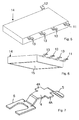
- Fig. 5 shows the housing 14 of the finished pressed-power semiconductor module in plan view.
- the connecting lugs 11, 12, 13 are led out laterally out of the housing.
- the terminals of the terminal lugs 11, 12, 13 lie on the opposite side of the substrate 9 of the housing 14, so that the component can be easily soldered in SMD technology, for example on a circuit board.
- Fig. 6 shows the same component from the bottom, wherein the flat DCB surface 15 can be pressed on the housing bottom for improved heat dissipation to a heat sink.
- the connection tabs are led out at the top of the housing.
- FIGS. 7 to 9 show an alternative embodiment of the contact element 1, which differs from that with reference to the Figures 1 and 2 described contact element characterized in that its first approach 5 is flat and the second approach 6 is formed mouth-shaped.
- the mutually corresponding sections are provided with the same reference numerals.
- a mouth-shaped projection 6 prevents movement of the approach of the adjacent contact element transversely to the longitudinal direction of the contact element.
- the mouth-shaped projection 6 has an outwardly tapering cutout 6A, so that an offset of joined together Contact elements is avoided even in the longitudinal direction.
- the first projection 5 has rounded corners whose contour corresponds to the contour of the inner section of the cutout 6A of the second projection 6.
- the first projection 5 of the one contact element 1 fits exactly into the second projection 6 of the other contact element 1. With the larger contact surface of the first projection 5, the contact with the substrate 9 is further improved.
- FIG. 9 shows that the first flat projection 5 of the contact element 1 relative to the second plate-shaped projection 6 is set lower, ie the distance between the first projection 5 and the connecting piece 4 is greater than the distance between the second projection 6 and the connecting piece 8. This allows height differences on the substrate 9 compensate.
- Fig. 10 shows a possible application of the contact element 1 of the FIGS. 7 to 9 for contacting the diodes 8 on the plus side of the substrate 9, wherein the lower-lying projection 5 of the contact elements 1 rests on the lower lying contact surface of the metallization 10 and the higher-lying projection 6 on the higher contact surface of the diode (chip) 8.
- the contact element 1 " On the minus side of the substrate 9 there is a similar application for the contact element 1 ", which electrically connects one of the diodes 8 to the external connection lug 11.
- the lower-lying projection 5 of the contact element 1 allows contacting on the wide flat contact surface of the substrate 9, which also saves a solder preform.
Landscapes
- Structures For Mounting Electric Components On Printed Circuit Boards (AREA)
Priority Applications (1)
| Application Number | Priority Date | Filing Date | Title |
|---|---|---|---|
| EP14164812.1A EP2933836B1 (fr) | 2014-04-15 | 2014-04-15 | Module semi-conducteur de puissance |
Applications Claiming Priority (1)
| Application Number | Priority Date | Filing Date | Title |
|---|---|---|---|
| EP14164812.1A EP2933836B1 (fr) | 2014-04-15 | 2014-04-15 | Module semi-conducteur de puissance |
Publications (2)
| Publication Number | Publication Date |
|---|---|
| EP2933836A1 true EP2933836A1 (fr) | 2015-10-21 |
| EP2933836B1 EP2933836B1 (fr) | 2020-10-14 |
Family
ID=50543442
Family Applications (1)
| Application Number | Title | Priority Date | Filing Date |
|---|---|---|---|
| EP14164812.1A Active EP2933836B1 (fr) | 2014-04-15 | 2014-04-15 | Module semi-conducteur de puissance |
Country Status (1)
| Country | Link |
|---|---|
| EP (1) | EP2933836B1 (fr) |
Cited By (1)
| Publication number | Priority date | Publication date | Assignee | Title |
|---|---|---|---|---|
| DE102021206587A1 (de) | 2021-06-25 | 2022-12-29 | Robert Bosch Gesellschaft mit beschränkter Haftung | Elektrische Anordnung mit Positionierhilfe und Herstellungsverfahren |
Citations (8)
| Publication number | Priority date | Publication date | Assignee | Title |
|---|---|---|---|---|
| EP0155473A1 (fr) | 1984-02-23 | 1985-09-25 | BROWN, BOVERI & CIE Aktiengesellschaft | Module pour dispositifs semiconducteurs de puissance et son procédé de fabrication |
| DE10316355B3 (de) | 2003-04-10 | 2004-07-01 | Semikron Elektronik Gmbh | Leistungshalbeitermodul mit flexibler äusserer Anschlussbelegung |
| DE10103084B4 (de) | 2001-01-24 | 2006-08-03 | Infineon Technologies Ag | Halbleitermodul und Verfahren zu seiner Herstellung |
| EP1713124A2 (fr) * | 2005-04-12 | 2006-10-18 | Semikron Elektronik GmbH & Co. KG Patentabteilung | Module semiconducteur de puissance avec des pistes de connexion et avec des éléments de connexion qui affleurent les pistes de connexion. |
| DE102005045100A1 (de) | 2005-09-21 | 2007-03-29 | Infineon Technologies Ag | Verfahren zum Herstellen eines Leistungshalbleitermoduls |
| US20070138624A1 (en) * | 2005-12-19 | 2007-06-21 | Mitsubishi Electric Corporation | Semiconductor device |
| EP1976358A2 (fr) | 2007-03-28 | 2008-10-01 | IXYS Semiconductor GmbH | Agencement d'au moins un module semi-conducteur de puissance et une plaque conductrice |
| US20120104621A1 (en) * | 2010-11-01 | 2012-05-03 | Samsung Electro-Mechanics Co., Ltd. | Power package module and method for fabricating the same |
-
2014
- 2014-04-15 EP EP14164812.1A patent/EP2933836B1/fr active Active
Patent Citations (9)
| Publication number | Priority date | Publication date | Assignee | Title |
|---|---|---|---|---|
| EP0155473A1 (fr) | 1984-02-23 | 1985-09-25 | BROWN, BOVERI & CIE Aktiengesellschaft | Module pour dispositifs semiconducteurs de puissance et son procédé de fabrication |
| DE10103084B4 (de) | 2001-01-24 | 2006-08-03 | Infineon Technologies Ag | Halbleitermodul und Verfahren zu seiner Herstellung |
| DE10316355B3 (de) | 2003-04-10 | 2004-07-01 | Semikron Elektronik Gmbh | Leistungshalbeitermodul mit flexibler äusserer Anschlussbelegung |
| EP1713124A2 (fr) * | 2005-04-12 | 2006-10-18 | Semikron Elektronik GmbH & Co. KG Patentabteilung | Module semiconducteur de puissance avec des pistes de connexion et avec des éléments de connexion qui affleurent les pistes de connexion. |
| DE102005016650A1 (de) | 2005-04-12 | 2006-11-02 | Semikron Elektronik Gmbh & Co. Kg | Leistungshalbleitermodul mit stoffbündig angeordneten Anschlusselementen |
| DE102005045100A1 (de) | 2005-09-21 | 2007-03-29 | Infineon Technologies Ag | Verfahren zum Herstellen eines Leistungshalbleitermoduls |
| US20070138624A1 (en) * | 2005-12-19 | 2007-06-21 | Mitsubishi Electric Corporation | Semiconductor device |
| EP1976358A2 (fr) | 2007-03-28 | 2008-10-01 | IXYS Semiconductor GmbH | Agencement d'au moins un module semi-conducteur de puissance et une plaque conductrice |
| US20120104621A1 (en) * | 2010-11-01 | 2012-05-03 | Samsung Electro-Mechanics Co., Ltd. | Power package module and method for fabricating the same |
Cited By (1)
| Publication number | Priority date | Publication date | Assignee | Title |
|---|---|---|---|---|
| DE102021206587A1 (de) | 2021-06-25 | 2022-12-29 | Robert Bosch Gesellschaft mit beschränkter Haftung | Elektrische Anordnung mit Positionierhilfe und Herstellungsverfahren |
Also Published As
| Publication number | Publication date |
|---|---|
| EP2933836B1 (fr) | 2020-10-14 |
Similar Documents
| Publication | Publication Date | Title |
|---|---|---|
| DE102011083223B4 (de) | Leistungshalbleitermodul mit integrierter Dickschichtleiterplatte | |
| DE102019112935B4 (de) | Halbleitermodul | |
| DE102017200256B4 (de) | Elektrodenanschluss, Halbleitervorrichtung und Leistungswandlungsvorrichtung | |
| DE102013100701B4 (de) | Halbleitermodulanordnung und verfahren zur herstellung einer halbleitermodulanordnung | |
| DE102011082781B4 (de) | Halbleitervorrichtung mit einer plattenelektrode zum verbinden einer mehrzahl an halbleiterchips | |
| DE102015122259B4 (de) | Halbleitervorrichtungen mit einer porösen Isolationsschicht | |
| DE102018200830B4 (de) | Halbleitervorrichtung | |
| DE102006045939B4 (de) | Leistungshalbleitermodul mit verbesserter Temperaturwechselstabilität | |
| WO2016134804A1 (fr) | Composant électrique et procédé de fabrication d'un composant électrique | |
| WO2004109812A2 (fr) | Boitier destine a un composant rayonnant, procede de fabrication et composant rayonnant | |
| DE102018206482B4 (de) | Halbleiterbauelement mit einem Verbundwerkstoffclip aus Verbundmaterial | |
| DE102008035911A1 (de) | Verfahren zum Herstellen eines integrierten Schaltungsmoduls | |
| DE102009047555A1 (de) | Elektrischer Steckverbinder niedriger Bauhöhe | |
| DE102020105267A1 (de) | Halbleitervorrichtung und Verfahren zur Herstellung derselben | |
| DE202014003171U1 (de) | Leistungshalbleitermodul | |
| EP3619739B1 (fr) | Module à semi-conducteur | |
| DE102013100700B3 (de) | Verfahren zur herstellung einer halbleitermodulanordnung | |
| EP3770959A1 (fr) | Procédé de connexion pour modules de puissance à une barre conductrice du réseau intermédiaire | |
| DE112015005593B4 (de) | Leistungsmodul | |
| EP4141923A1 (fr) | Composant semi-conducteur de puissance et procédé de fabrication d'un composant semi-conducteur de puissance | |
| EP2933836B1 (fr) | Module semi-conducteur de puissance | |
| DE10357789B4 (de) | Leistungs-Halbleitervorrichtung | |
| DE19902462B4 (de) | Halbleiterbauelement mit Chip-on-Chip-Aufbau | |
| DE102016209604B4 (de) | Halbleitervorrichtung und Leistungswandlungsvorrichtung | |
| DE112020002845T5 (de) | Halbleitervorrichtung |
Legal Events
| Date | Code | Title | Description |
|---|---|---|---|
| PUAI | Public reference made under article 153(3) epc to a published international application that has entered the european phase |
Free format text: ORIGINAL CODE: 0009012 |
|
| AK | Designated contracting states |
Kind code of ref document: A1 Designated state(s): AL AT BE BG CH CY CZ DE DK EE ES FI FR GB GR HR HU IE IS IT LI LT LU LV MC MK MT NL NO PL PT RO RS SE SI SK SM TR |
|
| AX | Request for extension of the european patent |
Extension state: BA ME |
|
| 17P | Request for examination filed |
Effective date: 20160408 |
|
| RBV | Designated contracting states (corrected) |
Designated state(s): AL AT BE BG CH CY CZ DE DK EE ES FI FR GB GR HR HU IE IS IT LI LT LU LV MC MK MT NL NO PL PT RO RS SE SI SK SM TR |
|
| STAA | Information on the status of an ep patent application or granted ep patent |
Free format text: STATUS: EXAMINATION IS IN PROGRESS |
|
| 17Q | First examination report despatched |
Effective date: 20190919 |
|
| GRAP | Despatch of communication of intention to grant a patent |
Free format text: ORIGINAL CODE: EPIDOSNIGR1 |
|
| STAA | Information on the status of an ep patent application or granted ep patent |
Free format text: STATUS: GRANT OF PATENT IS INTENDED |
|
| INTG | Intention to grant announced |
Effective date: 20200507 |
|
| GRAS | Grant fee paid |
Free format text: ORIGINAL CODE: EPIDOSNIGR3 |
|
| GRAA | (expected) grant |
Free format text: ORIGINAL CODE: 0009210 |
|
| STAA | Information on the status of an ep patent application or granted ep patent |
Free format text: STATUS: THE PATENT HAS BEEN GRANTED |
|
| AK | Designated contracting states |
Kind code of ref document: B1 Designated state(s): AL AT BE BG CH CY CZ DE DK EE ES FI FR GB GR HR HU IE IS IT LI LT LU LV MC MK MT NL NO PL PT RO RS SE SI SK SM TR |
|
| REG | Reference to a national code |
Ref country code: GB Ref legal event code: FG4D Free format text: NOT ENGLISH |
|
| REG | Reference to a national code |
Ref country code: AT Ref legal event code: REF Ref document number: 1324416 Country of ref document: AT Kind code of ref document: T Effective date: 20201015 Ref country code: CH Ref legal event code: EP |
|
| REG | Reference to a national code |
Ref country code: DE Ref legal event code: R096 Ref document number: 502014014875 Country of ref document: DE |
|
| REG | Reference to a national code |
Ref country code: IE Ref legal event code: FG4D Free format text: LANGUAGE OF EP DOCUMENT: GERMAN |
|
| REG | Reference to a national code |
Ref country code: NL Ref legal event code: MP Effective date: 20201014 |
|
| PG25 | Lapsed in a contracting state [announced via postgrant information from national office to epo] |
Ref country code: GR Free format text: LAPSE BECAUSE OF FAILURE TO SUBMIT A TRANSLATION OF THE DESCRIPTION OR TO PAY THE FEE WITHIN THE PRESCRIBED TIME-LIMIT Effective date: 20210115 Ref country code: FI Free format text: LAPSE BECAUSE OF FAILURE TO SUBMIT A TRANSLATION OF THE DESCRIPTION OR TO PAY THE FEE WITHIN THE PRESCRIBED TIME-LIMIT Effective date: 20201014 Ref country code: RS Free format text: LAPSE BECAUSE OF FAILURE TO SUBMIT A TRANSLATION OF THE DESCRIPTION OR TO PAY THE FEE WITHIN THE PRESCRIBED TIME-LIMIT Effective date: 20201014 Ref country code: NO Free format text: LAPSE BECAUSE OF FAILURE TO SUBMIT A TRANSLATION OF THE DESCRIPTION OR TO PAY THE FEE WITHIN THE PRESCRIBED TIME-LIMIT Effective date: 20210114 Ref country code: NL Free format text: LAPSE BECAUSE OF FAILURE TO SUBMIT A TRANSLATION OF THE DESCRIPTION OR TO PAY THE FEE WITHIN THE PRESCRIBED TIME-LIMIT Effective date: 20201014 Ref country code: PT Free format text: LAPSE BECAUSE OF FAILURE TO SUBMIT A TRANSLATION OF THE DESCRIPTION OR TO PAY THE FEE WITHIN THE PRESCRIBED TIME-LIMIT Effective date: 20210215 |
|
| REG | Reference to a national code |
Ref country code: LT Ref legal event code: MG4D |
|
| PG25 | Lapsed in a contracting state [announced via postgrant information from national office to epo] |
Ref country code: SE Free format text: LAPSE BECAUSE OF FAILURE TO SUBMIT A TRANSLATION OF THE DESCRIPTION OR TO PAY THE FEE WITHIN THE PRESCRIBED TIME-LIMIT Effective date: 20201014 Ref country code: LV Free format text: LAPSE BECAUSE OF FAILURE TO SUBMIT A TRANSLATION OF THE DESCRIPTION OR TO PAY THE FEE WITHIN THE PRESCRIBED TIME-LIMIT Effective date: 20201014 Ref country code: IS Free format text: LAPSE BECAUSE OF FAILURE TO SUBMIT A TRANSLATION OF THE DESCRIPTION OR TO PAY THE FEE WITHIN THE PRESCRIBED TIME-LIMIT Effective date: 20210214 Ref country code: PL Free format text: LAPSE BECAUSE OF FAILURE TO SUBMIT A TRANSLATION OF THE DESCRIPTION OR TO PAY THE FEE WITHIN THE PRESCRIBED TIME-LIMIT Effective date: 20201014 Ref country code: ES Free format text: LAPSE BECAUSE OF FAILURE TO SUBMIT A TRANSLATION OF THE DESCRIPTION OR TO PAY THE FEE WITHIN THE PRESCRIBED TIME-LIMIT Effective date: 20201014 Ref country code: BG Free format text: LAPSE BECAUSE OF FAILURE TO SUBMIT A TRANSLATION OF THE DESCRIPTION OR TO PAY THE FEE WITHIN THE PRESCRIBED TIME-LIMIT Effective date: 20210114 |
|
| PG25 | Lapsed in a contracting state [announced via postgrant information from national office to epo] |
Ref country code: HR Free format text: LAPSE BECAUSE OF FAILURE TO SUBMIT A TRANSLATION OF THE DESCRIPTION OR TO PAY THE FEE WITHIN THE PRESCRIBED TIME-LIMIT Effective date: 20201014 |
|
| REG | Reference to a national code |
Ref country code: DE Ref legal event code: R097 Ref document number: 502014014875 Country of ref document: DE |
|
| PG25 | Lapsed in a contracting state [announced via postgrant information from national office to epo] |
Ref country code: SK Free format text: LAPSE BECAUSE OF FAILURE TO SUBMIT A TRANSLATION OF THE DESCRIPTION OR TO PAY THE FEE WITHIN THE PRESCRIBED TIME-LIMIT Effective date: 20201014 Ref country code: RO Free format text: LAPSE BECAUSE OF FAILURE TO SUBMIT A TRANSLATION OF THE DESCRIPTION OR TO PAY THE FEE WITHIN THE PRESCRIBED TIME-LIMIT Effective date: 20201014 Ref country code: LT Free format text: LAPSE BECAUSE OF FAILURE TO SUBMIT A TRANSLATION OF THE DESCRIPTION OR TO PAY THE FEE WITHIN THE PRESCRIBED TIME-LIMIT Effective date: 20201014 Ref country code: EE Free format text: LAPSE BECAUSE OF FAILURE TO SUBMIT A TRANSLATION OF THE DESCRIPTION OR TO PAY THE FEE WITHIN THE PRESCRIBED TIME-LIMIT Effective date: 20201014 Ref country code: CZ Free format text: LAPSE BECAUSE OF FAILURE TO SUBMIT A TRANSLATION OF THE DESCRIPTION OR TO PAY THE FEE WITHIN THE PRESCRIBED TIME-LIMIT Effective date: 20201014 Ref country code: SM Free format text: LAPSE BECAUSE OF FAILURE TO SUBMIT A TRANSLATION OF THE DESCRIPTION OR TO PAY THE FEE WITHIN THE PRESCRIBED TIME-LIMIT Effective date: 20201014 |
|
| PLBE | No opposition filed within time limit |
Free format text: ORIGINAL CODE: 0009261 |
|
| STAA | Information on the status of an ep patent application or granted ep patent |
Free format text: STATUS: NO OPPOSITION FILED WITHIN TIME LIMIT |
|
| PG25 | Lapsed in a contracting state [announced via postgrant information from national office to epo] |
Ref country code: DK Free format text: LAPSE BECAUSE OF FAILURE TO SUBMIT A TRANSLATION OF THE DESCRIPTION OR TO PAY THE FEE WITHIN THE PRESCRIBED TIME-LIMIT Effective date: 20201014 |
|
| 26N | No opposition filed |
Effective date: 20210715 |
|
| PG25 | Lapsed in a contracting state [announced via postgrant information from national office to epo] |
Ref country code: AL Free format text: LAPSE BECAUSE OF FAILURE TO SUBMIT A TRANSLATION OF THE DESCRIPTION OR TO PAY THE FEE WITHIN THE PRESCRIBED TIME-LIMIT Effective date: 20201014 |
|
| PG25 | Lapsed in a contracting state [announced via postgrant information from national office to epo] |
Ref country code: SI Free format text: LAPSE BECAUSE OF FAILURE TO SUBMIT A TRANSLATION OF THE DESCRIPTION OR TO PAY THE FEE WITHIN THE PRESCRIBED TIME-LIMIT Effective date: 20201014 Ref country code: MC Free format text: LAPSE BECAUSE OF FAILURE TO SUBMIT A TRANSLATION OF THE DESCRIPTION OR TO PAY THE FEE WITHIN THE PRESCRIBED TIME-LIMIT Effective date: 20201014 |
|
| PG25 | Lapsed in a contracting state [announced via postgrant information from national office to epo] |
Ref country code: LU Free format text: LAPSE BECAUSE OF NON-PAYMENT OF DUE FEES Effective date: 20210415 |
|
| REG | Reference to a national code |
Ref country code: BE Ref legal event code: MM Effective date: 20210430 |
|
| PG25 | Lapsed in a contracting state [announced via postgrant information from national office to epo] |
Ref country code: LI Free format text: LAPSE BECAUSE OF NON-PAYMENT OF DUE FEES Effective date: 20210430 Ref country code: CH Free format text: LAPSE BECAUSE OF NON-PAYMENT OF DUE FEES Effective date: 20210430 |
|
| PG25 | Lapsed in a contracting state [announced via postgrant information from national office to epo] |
Ref country code: IE Free format text: LAPSE BECAUSE OF NON-PAYMENT OF DUE FEES Effective date: 20210415 |
|
| PG25 | Lapsed in a contracting state [announced via postgrant information from national office to epo] |
Ref country code: IS Free format text: LAPSE BECAUSE OF FAILURE TO SUBMIT A TRANSLATION OF THE DESCRIPTION OR TO PAY THE FEE WITHIN THE PRESCRIBED TIME-LIMIT Effective date: 20210214 |
|
| REG | Reference to a national code |
Ref country code: AT Ref legal event code: MM01 Ref document number: 1324416 Country of ref document: AT Kind code of ref document: T Effective date: 20210415 |
|
| PG25 | Lapsed in a contracting state [announced via postgrant information from national office to epo] |
Ref country code: BE Free format text: LAPSE BECAUSE OF NON-PAYMENT OF DUE FEES Effective date: 20210430 |
|
| PG25 | Lapsed in a contracting state [announced via postgrant information from national office to epo] |
Ref country code: AT Free format text: LAPSE BECAUSE OF NON-PAYMENT OF DUE FEES Effective date: 20210415 |
|
| PG25 | Lapsed in a contracting state [announced via postgrant information from national office to epo] |
Ref country code: HU Free format text: LAPSE BECAUSE OF FAILURE TO SUBMIT A TRANSLATION OF THE DESCRIPTION OR TO PAY THE FEE WITHIN THE PRESCRIBED TIME-LIMIT; INVALID AB INITIO Effective date: 20140415 |
|
| PG25 | Lapsed in a contracting state [announced via postgrant information from national office to epo] |
Ref country code: CY Free format text: LAPSE BECAUSE OF FAILURE TO SUBMIT A TRANSLATION OF THE DESCRIPTION OR TO PAY THE FEE WITHIN THE PRESCRIBED TIME-LIMIT Effective date: 20201014 |
|
| P01 | Opt-out of the competence of the unified patent court (upc) registered |
Effective date: 20230607 |
|
| PG25 | Lapsed in a contracting state [announced via postgrant information from national office to epo] |
Ref country code: MK Free format text: LAPSE BECAUSE OF FAILURE TO SUBMIT A TRANSLATION OF THE DESCRIPTION OR TO PAY THE FEE WITHIN THE PRESCRIBED TIME-LIMIT Effective date: 20201014 |
|
| PG25 | Lapsed in a contracting state [announced via postgrant information from national office to epo] |
Ref country code: TR Free format text: LAPSE BECAUSE OF FAILURE TO SUBMIT A TRANSLATION OF THE DESCRIPTION OR TO PAY THE FEE WITHIN THE PRESCRIBED TIME-LIMIT Effective date: 20201014 |
|
| PG25 | Lapsed in a contracting state [announced via postgrant information from national office to epo] |
Ref country code: MT Free format text: LAPSE BECAUSE OF FAILURE TO SUBMIT A TRANSLATION OF THE DESCRIPTION OR TO PAY THE FEE WITHIN THE PRESCRIBED TIME-LIMIT Effective date: 20201014 |
|
| REG | Reference to a national code |
Ref country code: DE Ref legal event code: R079 Ref document number: 502014014875 Country of ref document: DE Free format text: PREVIOUS MAIN CLASS: H01L0025070000 Ipc: H10D0080200000 |
|
| PGFP | Annual fee paid to national office [announced via postgrant information from national office to epo] |
Ref country code: DE Payment date: 20250305 Year of fee payment: 12 |
|
| PGFP | Annual fee paid to national office [announced via postgrant information from national office to epo] |
Ref country code: GB Payment date: 20260312 Year of fee payment: 13 |
|
| PGFP | Annual fee paid to national office [announced via postgrant information from national office to epo] |
Ref country code: IT Payment date: 20260320 Year of fee payment: 13 |
|
| PGFP | Annual fee paid to national office [announced via postgrant information from national office to epo] |
Ref country code: FR Payment date: 20260309 Year of fee payment: 13 |