EP2933878B1 - Antennenvorrichtung - Google Patents
Antennenvorrichtung Download PDFInfo
- Publication number
- EP2933878B1 EP2933878B1 EP15163088.6A EP15163088A EP2933878B1 EP 2933878 B1 EP2933878 B1 EP 2933878B1 EP 15163088 A EP15163088 A EP 15163088A EP 2933878 B1 EP2933878 B1 EP 2933878B1
- Authority
- EP
- European Patent Office
- Prior art keywords
- protrusion portions
- antenna apparatus
- substrate
- support part
- coil portion
- Prior art date
- Legal status (The legal status is an assumption and is not a legal conclusion. Google has not performed a legal analysis and makes no representation as to the accuracy of the status listed.)
- Active
Links
Images


Classifications
-
- H—ELECTRICITY
- H01—ELECTRIC ELEMENTS
- H01Q—ANTENNAS, i.e. RADIO AERIALS
- H01Q7/00—Loop antennas with a substantially uniform current distribution around the loop and having a directional radiation pattern in a plane perpendicular to the plane of the loop
-
- H—ELECTRICITY
- H01—ELECTRIC ELEMENTS
- H01Q—ANTENNAS, i.e. RADIO AERIALS
- H01Q1/00—Details of, or arrangements associated with, antennas
- H01Q1/12—Supports; Mounting means
- H01Q1/22—Supports; Mounting means by structural association with other equipment or articles
- H01Q1/24—Supports; Mounting means by structural association with other equipment or articles with receiving set
- H01Q1/241—Supports; Mounting means by structural association with other equipment or articles with receiving set used in mobile communications, e.g. GSM
- H01Q1/242—Supports; Mounting means by structural association with other equipment or articles with receiving set used in mobile communications, e.g. GSM specially adapted for hand-held use
- H01Q1/243—Supports; Mounting means by structural association with other equipment or articles with receiving set used in mobile communications, e.g. GSM specially adapted for hand-held use with built-in antennas
-
- G—PHYSICS
- G06—COMPUTING OR CALCULATING; COUNTING
- G06K—GRAPHICAL DATA READING; PRESENTATION OF DATA; RECORD CARRIERS; HANDLING RECORD CARRIERS
- G06K7/00—Methods or arrangements for sensing record carriers, e.g. for reading patterns
- G06K7/10—Methods or arrangements for sensing record carriers, e.g. for reading patterns by electromagnetic radiation, e.g. optical sensing; by corpuscular radiation
- G06K7/10009—Methods or arrangements for sensing record carriers, e.g. for reading patterns by electromagnetic radiation, e.g. optical sensing; by corpuscular radiation sensing by radiation using wavelengths larger than 0.1 mm, e.g. radio-waves or microwaves
- G06K7/10316—Methods or arrangements for sensing record carriers, e.g. for reading patterns by electromagnetic radiation, e.g. optical sensing; by corpuscular radiation sensing by radiation using wavelengths larger than 0.1 mm, e.g. radio-waves or microwaves using at least one antenna particularly designed for interrogating the wireless record carriers
- G06K7/10336—Methods or arrangements for sensing record carriers, e.g. for reading patterns by electromagnetic radiation, e.g. optical sensing; by corpuscular radiation sensing by radiation using wavelengths larger than 0.1 mm, e.g. radio-waves or microwaves using at least one antenna particularly designed for interrogating the wireless record carriers the antenna being of the near field type, inductive coil
-
- H—ELECTRICITY
- H01—ELECTRIC ELEMENTS
- H01Q—ANTENNAS, i.e. RADIO AERIALS
- H01Q1/00—Details of, or arrangements associated with, antennas
- H01Q1/12—Supports; Mounting means
- H01Q1/1207—Supports; Mounting means for fastening a rigid aerial element
-
- H—ELECTRICITY
- H01—ELECTRIC ELEMENTS
- H01Q—ANTENNAS, i.e. RADIO AERIALS
- H01Q1/00—Details of, or arrangements associated with, antennas
- H01Q1/36—Structural form of radiating elements, e.g. cone, spiral, umbrella; Particular materials used therewith
- H01Q1/38—Structural form of radiating elements, e.g. cone, spiral, umbrella; Particular materials used therewith formed by a conductive layer on an insulating support
-
- H—ELECTRICITY
- H01—ELECTRIC ELEMENTS
- H01Q—ANTENNAS, i.e. RADIO AERIALS
- H01Q7/00—Loop antennas with a substantially uniform current distribution around the loop and having a directional radiation pattern in a plane perpendicular to the plane of the loop
- H01Q7/06—Loop antennas with a substantially uniform current distribution around the loop and having a directional radiation pattern in a plane perpendicular to the plane of the loop with core of ferromagnetic material
- H01Q7/08—Ferrite rod or like elongated core
Definitions
- the following description relates to an antenna device, and an electronic component including the same.
- NFC near field communications
- portable terminals so as to enable communications between the portable terminals, such as data exchanges, and personal authentication.
- NFC refers to a non-contact type near field communications module utilizing a frequency band of about 13.56 megahertz (MHz), and in order to use a radio signal within the above-mentioned frequency band, a separate antenna may be needed.
- An NFC antenna generally uses a loop pattern and is formed in a planar shape so as to be mounted in a battery or on a cover of the portable terminal.
- the invention is as defined in claim 1.
- the core member is mounted on a first substrate through pad parts disposed on the mounting surfaces of the second protrusion portions, respectively.
- first and second protrusion portions are disposed on the support part so that the core member has an 'H' shape.
- the first protrusion portions have end surfaces through which magnetic flux enters and exits.
- a length of the first protrusion portions protruding from the support part is different from a length of one of the second protrusion portions protruding from the support part.
- the core member has an angle of 180° of a direction in which the magnetic flux enters one of the end surfaces of the core member with respect to a direction in which the magnetic flux exits from one of the end surfaces of the core member.
- the coil portion is wound around the first and second core portions.
- the coil portion is wound around the third core portion.
- the coil portion is wound around each of the first, second, and third core portions.
- NFC near field communications
- FIG. 1 is a perspective view illustrating an example of an antenna apparatus not according to an embodiment in the present invention.
- an antenna apparatus includes a core member 100 and a coil portion 200 wound around the core member 100.
- this is simply an example of the coil portion 200 being wound around the core member 100 and thus is not limited thereto.
- the coil portion 200 is not limited to a single wire and may be formed by a stranded wire or more than one wire.
- FIG. 1 illustrates the coil portion 200a being wound around almost an entire surface of a support part 110 of the core member 100, such wounding is not limited thereto and thus the winding can cover more or less of the surface of the support part 110.
- the coil portion 200 is wound around at least one of a support part 110 and a plurality of first protrusion portions 120 of the core member 100.
- the coil portion wound around the support part 110 will be designated by 200a (see FIG. 1 )and the coil portion wound around the plurality of first protrusion portions 120 will be designated by 200b (see FIG. 6A ).
- a coil portion having common characteristics applicable to both a coil portion 200a and a coil portion 200b will be designated by 200.
- the core member 100 includes the support part 110, the plurality of first protrusion portions 120, and a plurality of second protrusion portions 130.
- the support part 110 includes an end surface having a polygonal shape or a circular shape so that the antenna apparatus is mounted on a first substrate 400 to thereby facilitate the miniaturization of the antenna apparatus.
- the support part 110 is not limited to the above discussed shapes and thus may have any other shape suitable for mounting the antenna apparatus on the first substrate 400.
- FIG. 3A illustrates the second protrusion portion 130a and 130b and first and second pad parts 310 and 320, to be later described, to be separate structural elements from the support part 110, the first and second protrusion portions 130a and 130b and the first and second pad parts 310 and 320 may be integral parts of the support part 110. Referring to FIG.
- the support part 110 has a hexahedral shape or a cylindrical shape.
- directions of a hexahedron will be defined in order to clearly describe the core member 100.
- L, W and T illustrated in FIG. 1 refer to a length direction, a width direction, and a thickness direction, respectively.
- the plurality of first protrusion portions 120 are disposed on one surface of the support part 110 and the plurality of second protrusion portions 130 are disposed on the other surface of the support part 110, opposite to one surface of the support part 110.
- the surface of the support part 110 on which the plurality of first protrusion portions 120 are disposed will be referred to as one surface or a first surface of the support part 110
- the surface of the support part 110 on which the plurality of second protrusion portions 130 are disposed will be referred to as the other surface or a second surface of the support part 110, opposite to the one surface or first surface of the support part 110.
- the plurality of first protrusion portions 120 are two first protrusion portions 120a and 120b, in which the two first protrusion portions 120a and 120b are disposed on one surface of the support part 110 at both ends thereof in a length direction of the support part 110, respectively.
- the disposition of the plurality of first protrusion portions 120 is not limited thereto.
- the disposition thereof may be provided in various manners.
- the length direction of the support part 110 refers to a direction of a side thereof having a greatest length among sides of the support part 110.
- the plurality of second protrusion portions 130 includes second protrusion portions 130a and 130b, which are disposed on the other surface of the support part 110, opposite to one surface of the support part 110 at both ends thereof in the length direction, respectively.
- the disposition of the plurality of second protrusion portions 130 is not limited thereto, and is not limited to a particular example as long as the second protrusion portion 130 has a mounting surface such that the core member 100 is mounted on a first substrate 400 (see FIG. 3A ) through first and second pad parts 310 and 320 (see FIG. 3A ).
- a case in which the plurality of second protrusion portions 130 have a plurality of mounting surfaces, respectively, will be described with reference to FIG. 2 .
- the plurality of first protrusion portions 120 are disposed on one surface of support part 110, and the plurality of second protrusion portions 130 are disposed on the other surface of the support part 110, opposite to one surface of the support part 110, so as to protrude in opposing directions. Accordingly, the plurality of first protrusion portions 120 are collinear with the support part 110, and the plurality of second protrusion portions 130 are collinear with the support part 110.
- the plurality of first protrusion portions 120 and the plurality of second protrusion portions 130 may have an overall pillar shape (see FIG. 1 ), but the shape of the first and second protrusion portions 120 and 130 is not limited thereto.
- the plurality first and second protrusion portions 120 and 130 among the components of the antenna apparatus are described to each have two protrusion portions, this is merely for ease of description and the number of the plurality of first and second protrusion portions 120 and 130 is not limited thereto.
- an end surface of each of the plurality of first protrusion portions 120 is illustrated as being a quadrangular shape, but the shape of the end surface of the first protrusion portion 120 is not limited thereto.
- each of the plurality of second protrusion portions 130 is also illustrated as being a quadrangular shape, but the shape of the end surface of the second protrusion portion 130 is not limited thereto. Further, the shapes of each of the plurality of first protrusion portions 120 and each of the plurality of second protrusion portions 130 may be distinct from one another.
- the two first protrusion portions 120a and 120b include two end surfaces 121a and 121b through which magnetic flux enters and exits, respectively.
- the magnetic flux in a case in which the magnetic flux exits from the end surface 121a of the first protrusion portion 120a, the magnetic flux enters the end surface 121b of the first protrusion portion 120b.
- the magnetic flux in a case in which the magnetic flux enters the end surface 121a of the first protrusion portion 120a, the magnetic flux exits from the end surface 121b of the first protrusion portion 120b.
- the entering and exiting of the magnetic flux is not limited thereto.
- the magnetic flux may enter and exit from other areas of the support part 110.
- the core member 100 is formed by combining a material, or the like including a magnetic material such as ferrite, or the like having a predetermined dielectric constant and permeability with a composite material such as ceramic, or the like, in order to transmit and receive an NFC signal within a low frequency band, by using a sintering scheme, a molding scheme, or the like.
- the core member 100 among the components of the antenna apparatus according to the embodiment in the present invention may have an "H" shape.
- the shape of the core member 100 is not limited thereto and thus the core member 100 may have any other shape or form.
- the core member 100 may have a "U" shape.
- each of the first two first protrusion portions 120a and 120b are disposed at each end of the support part 110 in a length direction, respectively.
- each of the second protrusion portions 130a and 130b are disposed on the support part 110 so as to be opposite to the two first protrusion portions 120a and 120b, respectively.
- first protrusion portions 120a and 120b have volumes greater than those of the second protrusion portions 130a and 130b, respectively. Therefore, in the antenna apparatus, the volumes of the first protrusion portions 120a and 120b associated with the entry and exit of the magnetic flux are formed to be greater than those of the second protrusion portions 130a and 130b, whereby efficiency of the entry and exit of the magnetic flux is increased and reliability of the antenna apparatus is improved.
- the relationship of volumes between the first protrusion portions 120a and 120b and the second protrusion portions 130a and 130b is not limited thereto. That is the first protrusion portions 120a and 120b and the second protrusion portions 130a and 130b may have the same volumes.
- the mounting surfaces 131a and 131b of the two second protrusion portions 130a and 130b are formed to have sufficiently great areas, respectively. Therefore, when the core member 100 is mounted on the first substrate 400 ( FIG. 3A ), a fixing strength there between is improved.
- the coil portion 200a is wound around the support part 110 so as to form the magnetic flux that enters and exits from the core member 100.
- the coil portion 200a is wound around the support part 110 in a single direction so that the magnetic flux enters or exits through the two first protrusion portions 120a and 120b.
- the coil portion 200a is wound around the support part 110 so as to transmit and receive a signal in a frequency band of about 13.56MHz to perform the NFC scheme.
- the coil portion 200a is electrically connected to a circuit part including an NFC chip (not illustrated) of the first substrate 400 (see FIG. 3A ).
- the coil portion 200a is wound around the support part 110 so as to perform transmission and reception of data with the external electronic device through the electromagnetic induction formed based on the entry and exit of the magnetic flux through the end surfaces 121a and 121b of the respective first protrusion portions 120a and 120b.
- the external electronic device includes an antenna capable of transmitting and receiving a signal in the same frequency band as that of the antenna apparatus.
- the coil portion 200a is electrically connected to the circuit part including the NFC chip through pad parts 310 and 320 (see FIG. 3A ) attached to the mounting surfaces 131a and 131b of the plurality of second protrusion portions 130, respectively.
- an outer circumferential surface of a metal wire formed of copper (Cu), or silver (Ag), and coated by applying an insulating coat formed of a polyurethane resin, or polyester resin, is used as the coil portion 200a.
- the coil portion 200a is not limited to a single wire and may be formed by a stranded wire or two or more wires.
- the coil portion 200a is wound around the support part 110 so as to surround the support part 110 in a circular manner as illustrated in FIG. 1 , but the winding of the coil portion 200a is not limited thereto.
- the coil portion 200a may be wound around the support part 110 so as to have the end surface thereof having the same shape as that of the end surface of the support part 110, for example, a quadrangular shape.
- the shape of the end surface of the coil portion 200a is not limited to the circular end surface, but the coil portion 200a may also have a polygonal end surface.
- FIG. 2 is a perspective view illustrating an example of the antenna apparatus illustrated in FIG. 1 at a different angle.
- the plurality of second protrusion portions 130 include the two second protrusion portions 130a and 130b by way of example. Furthermore, the two second protrusion portions 130a and 130b include the end surfaces 131a and 131b provided as the mounting surfaces allowing for the mounting on the first substrate 400 (see FIG. 4A ), respectively.
- the core member 100 is mounted on the first substrate 400 (see FIG. 3A ) through the first and second pad parts 310 and 320 (see FIG. 3A ) attached to the end surfaces 131a and 131b of the two second protrusion portions 130a and 130b, respectively.
- a side of the other surface of the support part 110 on which the two second protrusion portions 130a and 130b are disposed may be a side on which the first substrate 400 (see FIG. 3A ) is present.
- the entirety of the other surface of the support part 110 may not be provided as the mounting surface allowing for the mounting on the substrate, but the antenna apparatus may separately include the plurality of second protrusion portions 130 having the mounting surfaces 131a and 131b for allowing the mounting on the first substrate 400 ( FIG. 3A ), respectively.
- the support part 110 is spaced apart from the first substrate 400 (see FIG. 3A ) by a distance equal to a total of a height of each of the first and second pad parts 310 and 320 (see FIG. 3A ) and a height of each of the plurality of second protrusion portions 130.
- FIGS. 3A and 3B are views illustrating an example of an antenna apparatus not according to an embodiment in the present invention mounted on a first substrate.
- the two first protrusion portions 120a and 120b have the end surfaces 121a and 121b through which the magnetic flux enters and exits, so as to form the magnetic path, respectively.
- the two second protrusion portions 130a and 130b have the end surfaces 131a and 131b provided as the mounting surfaces, so as to perform a surface mount technology (SMT) on the first substrate 400 through the first and second pad parts 310 and 320, respectively.
- SMT surface mount technology
- the core member 100 is formed in the 'H' shape by way of example, so as to provide a common magnetic flux path, whereby eddy current loss is significantly reduced.
- the antenna apparatus is mounted on the first substrate 400 through the first and second pad parts 310 and 320 attached to the mounting surfaces 131a and 131b (see FIG. 2 ) of the two second protrusion portions 130a and 130b, respectively.
- the first substrate 400 is a substrate mounted in an interior of a portable terminal such as a smartphone, in which the circuit part having the NFC chip (not illustrated) is disposed on the first substrate 400.
- the first substrate 400 includes a plurality of active elements, a plurality of passive elements, integrated circuits (ICs).
- ICs integrated circuits
- a printed circuit board (PCB) is provided as the first substrate 400, but is not limited thereto.
- the antenna apparatus is mounted on one surface of the first substrate 400.
- the first and second pad parts 310 and 320 are positioned to be spaced apart from one another so as to perform an SMT on the first substrate 400.
- the antenna apparatus is electrically connected to the first substrate 400 by a soldering scheme in a state in which the first and second pad parts 310 and 320 are disposed on the first substrate 400 to be in contact therewith.
- a soldering scheme such scheme is not limited thereto and any other suitable connection scheme may be used, such as gluing or welding.
- FIG. 4A is a view illustrating an example of a first molding part included in the antenna apparatus mounted on the first substrate illustrated in FIG. 3A .
- an electronic component having the antenna apparatus mounted on the first substrate 400 further includes a first molding part 410 disposed between the two first protrusion portions 120a and 120b.
- the first molding part 410 is disposed between the two first protrusion portions 120a and 120b so that the end surfaces 121a and 121b of the first protrusion portions 120a and 120b are exposed externally.
- an epoxy molding compound EMC
- the molding compound is not limited thereto and any suitable molding compound may be used.
- FIG. 4A illustrates a case in which the end surfaces 121a and 121b of the first protrusion portions 120a and 120b are coplanar with the first molding part 410
- the position of the end surfaces 121a and 121b of the first protrusion portions 120a and 120b with respect to the first molding part 410 is not limited thereto.
- FIG. 4B is a view illustrating an example of a second molding part further included in the antenna apparatus mounted on the first substrate illustrated in FIG. 3A .
- the second molding part 420 is formed so as to encapsulate the support part 110, the two first protrusion portions 120a and 120b, and the two second protrusion portions 130a and 130b.
- the second molding part 420 is formed so as to cover both side surfaces of the support part 110 in the length direction while simultaneously covering the end surfaces 121a and 121b of the two first protrusion portions 120a and 120b.
- the second molding part 420 may serve as a cover for preventing external infiltration of foreign materials, or the like, there into.
- the antenna apparatus includes a chip structure by forming the first molding part 410 or the second molding part 420 therein, so as to allow for product miniaturization.
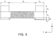
- FIG. 5 is a view illustrating lengths and heights of respective components of an example of an antenna apparatus according to an embodiment in the present invention.
- the antenna apparatus has a size of 8.0 ⁇ 1.3 ⁇ 4 millimeters (mm).
- lengths t1 and t3 of the respective first protrusion portions 120a and 120b in the length direction may each be 1.5mm. Further, since an entire length of the support part 110 in the length direction is 8mm, equal to a total of lengths (t1 + t2 + t3), the length t2, which is equal to a length of a portion of the support part 110, is 5mm.
- the first protrusion portions 120a and 120b may each have a height t4 of 0.5mm and the support part 110 may also have a height t5 of 0.5mm.
- the second protrusion portions 130a and 130b may each have a height t6 of 0.2mm and the first and second pad parts 310 and 320 may each have a height t7 of 0.1 mm.
- the height of the first protrusion portions 120 and the second protrusion portions 130 is not limited to the above-mentioned values.
- the height of the support part 110 and the first and second pad parts 310 and 320 is not limited to the above-mentioned values.
- the antenna apparatus may have a chip structure so as to allow for product miniaturization.
- FIGS. 6A and 6B are views illustrating an example in which a coil portion is wound around at a different position of an antenna apparatus not according to the present invention.
- the coil portion 200b is wound around the plurality of first protrusion portions 120.
- the coil portion 200b is wound around each of the two first protrusion portions 120a and 120b.
- the coil portion 200b is wound around the two first protrusion portions 120a and 120b in a single direction.
- the coil portion 200b includes a coil connecting portion that connects coil portions wound around the respective first protrusion portions 120a and 120b to one another.
- the coil portion 200b is connected to the first and second pad parts 310 and 320 (see FIG. 3A ) attached to the mounting surfaces 131a and 131b of the two second protrusion portions 130a and 130b, respectively.
- the number of coils of the coil portion 200b being wound around each of the two first protrusion portions 120a and 120b is determined based on a resonance frequency of the antenna apparatus so as to transmit and receive a signal in a frequency band of about 13.56MHz. Meanwhile, since the coil portion 200b is of the same material and shape as those of the aforementioned coil portion 200a wound around the support part 110, a repeated description thereof will be omitted for conciseness.
- the antenna apparatus includes the coil portion 200 wound around each of the plurality of first protrusion portions 120 and the support part 110.
- the coil portion 200a wound around the support part 110 and the coil portion 200b wound around the plurality of first protrusion portions 120 are both connected to the first and second pad parts 310 and 320 (see FIG. 3A ) attached to the mounting surfaces 131a and 131b of the two second protrusion portions 130a and 130b, respectively.
- coil portions 200a and 200b have the same material and shape as those described above, a repeated description thereof will be omitted for conciseness.
- FIGS. 7A through 7C are views illustrating examples of the plurality of first protrusion portions among components of the antenna apparatus illustrated in FIG. 1 .
- the two first protrusion portions 120a and 120b of the antenna apparatus have inclined end surfaces 121a and 121b, respectively but their shapes are not limited thereto and may have other shapes.
- the two end surfaces 121a and 121b have inclined angles different from one another.
- the inclined end surfaces 121a and 121b are formed to face outward in opposite directions (see FIG. 7A ), or are formed inwardly to face one another in a common direction (see FIG. 7B ).
- the orientations of the two end surfaces 121a and 121b are not limited thereto.
- one end surface 121a of the end surfaces 121a and 121b of the respective first protrusion portions 120a and 120b is inclined but is not limited thereto.
- the directions or the inclined angles of the respective end surfaces 121a and 121b are different from one another, and the direction of magnetic flux that enters and exits from the two end surfaces 121a and 121b and a shape of a magnetic path formed by the magnetic flux is changed.
- the shape of the core member 100 is not limited to the example illustrated in FIGS. 7A through 7C , and the core member 100 may be formed to have a width, a height, or a size such that the coil portion 200a may be sufficiently wound around the core member 100.
- a distance between the two first protrusion portions 120a and 120b and a distance between the two second protrusion portions 130a and 130b do not need to be the same as one another as illustrated in FIGS. 7A through 7C , the distances between the first protrusion portions and the distances between second protrusion portions may be different from one another.
- the two first protrusion portions 120a and 120b may have volumes greater than those of the two second protrusion portions 130a and 130b, respectively. Therefore, in the antenna apparatus, the volumes of the first protrusion portions 120a and 120b, associated with the entry and exit of the magnetic flux may be formed to be greater than those of the second protrusion portions 130a and 130b, whereby efficiency of the entry and exit of the magnetic flux is increased and reliability of the antenna apparatus is improved.
- the mounting surfaces 131a and 131b of the two second protrusion portions 130a and 130b are formed to have sufficiently great areas, respectively. Therefore, in the case in which the core member 100 is mounted on the first substrate 400 (see FIG. 3A ), fixing strength there between is improved.
- the antenna apparatus is not limited to the examples illustrated in FIGS. 1 through 7 .
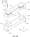
- FIG. 8A is an exploded view illustrating an example in which the coil portion is wound around the plurality of first protrusion portions in an antenna apparatus according to an embodiment in the present invention.
- an antenna apparatus includes the coil portion 200b wound around the plurality of first protrusion portions 120.
- the coil portion 200b is wound around each of the two first protrusion portions 120a and 120b.
- the antenna apparatus further includes a second substrate 220 having a cavity.
- the coil portion 200b is positioned in the cavity of the second substrate 220.
- the coil portion 200b is formed to surround the cavity of the second substrate 220, and the two first protrusion portions 120a and 120b are positioned in the cavity, such that the second substrate 220 in which the coil portion 200b is positioned is coupled to the core member 100.
- the shape and size of the cavity of the second substrate 220 is determined based on the shape, the number, and the height of the plurality of first protrusion portions 120 of the core member 100. For example, in the case in which the plurality of first protrusion portions 120 are the two first protrusion portions 120a and 120b, the cavity is formed correspondingly thereto.
- the second substrate 220 may have an end surface having a quadrangular shape, for example, a rectangle, so as to be coupled to the core member 100 to thereby form a chip shape.
- a length of the second substrate 220 and a width of the second substrate 220 may be similar to the length and the width of the support part 110, respectively, and a height of the substrate 220 may be formed so that the two first protrusion portions 120a and 120b may be securely positioned in the cavity.
- the coil portion 200b includes a coil connecting portion 210 that connects coil portions wound around the respective first protrusion portions 120a and 120b to one another.
- the coil connecting portion 210 is also formed in the cavity of the second substrate 220.
- the coil connecting portion 210 may be broken or loosened.
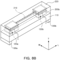
- FIG. 8B is a view illustrating an example in which the coil portion is wound around the plurality of first protrusion portions in an antenna apparatus not according to another embodiment, different from that of FIG. 8A .
- the coil portion 200b itself, directly wound around the two first protrusion portions 120a and 120b, is positioned in the cavity of the second substrate 220.
- the two first protrusion portions 120a and 120b themselves having the coil portion 200b wound there around are positioned in the cavity of the second substrate 220.
- a size of the cavity of the second substrate 220 illustrated in FIG. 8B is greater than that of the cavity of the second substrate 220 illustrated in FIG. 8A so that the coil portion 200b is positioned in the cavity, unlike the description thereof provided in FIG. 8A .
- FIG. 9 is a view illustrating a direction of magnetic flux in an antenna apparatus.
- an antenna apparatus forms a magnetic path having an angle of 180° of a direction in which the magnetic flux enters with respect to a direction in which the magnetic flux exits.
- the magnetic flux enters the end surface 121b of the first protrusion portion 120b.
- the magnetic flux exits from the end surface 121b of the first protrusion portion 120b, the magnetic flux enters the end surface 121a of the first protrusion portion 120a.
- a magnetic path is formed by disposing face to face an external electronic device using the NFC scheme and the antenna apparatus, and data is transmitted and received through two-way communications.
- FIGS. 10A and 10B are perspective views of an antenna apparatus not according to another embodiment in the present invention.
- an antenna apparatus includes a core member 500 and a coil portion 600a wound around the core member 500.
- the core member 500 includes a first core portion 510a, a second core portion 510b, and a third core portion 510c.
- the first core portion 510a includes a first end surface 511a through which magnetic flux enters and exits and a first mounting surface 512a, opposite to the first end surface 511a.
- the second core portion 510b includes a second end surface 511b through which the magnetic flux enters and exits and a second mounting surface 512b, opposite to the second end surface 511b.
- the first and second end surfaces 511a and 511b of the first and second core portions 510a and 510b, respectively, have polygonal or circular shapes so that the antenna apparatus is mounted on the substrate to thereby allow for product miniaturization.
- first and second core portions 510a and 510b have an overall pillar shape, but the shape of the first and second protrusion portions 510a and 510b is not limited thereto.
- the third core portion 510c is disposed between the first and second core portions 510a and 510b. More particularly, the first and second core portions 510a and 510b is disposed so as to be perpendicular to the third core portion 510c at both ends of the third core portion 510c in a length direction of the third core portion 510c.
- first core portion 510a and the second core portion 510b are disposed on both end surfaces of the third core portion 510c in the length direction, respectively.
- a coil portion is wound around the third core portion 510c (600a in FIG. 10A ), or is wound around each of the first and second core portions 511a and 511b (600b in FIG. 10B ).
- the coil portion 600a is wound around the third core portion 510c and transmits and receives a signal in a frequency band of about 13.56MHz to perform the NFC scheme.
- the coil portion 600a performs transmission and reception of data with an external electronic device through electromagnetic induction formed based on the entry and exit of the magnetic flux through the end surfaces 511a and 511b of the respective first and second core portions 510a and 510b.
- the external electronic device includes an antenna capable of transmitting and receiving a signal in the same frequency band as that of the antenna apparatus according to the other embodiment.
- the coil portion 600a is wound around the third core portion 510c in a circular manner as illustrated in FIG. 10A , but the winding of the coil portion 600a is not limited thereto.
- the coil portion 600a is wound to have the same shape of the end surface of the third core portion 510c.
- the coil portion 600a will be wound in a quadrangular shape.
- the coil portion 600a may be wound around the third core portion 510c in an inclined manner (not illustrated).
- the antenna apparatus includes the coil portion 600b wound around each of the first and second core portions 510a and 510b. More particularly, the coil portion 600b is wound along the first and second end surfaces 511a and 511b.
- the number of turns of the coil portion 600b being wound around each of the first and second core portions 510a and 510b is determined based on a resonance frequency of the antenna apparatus so as to transmit and receive a signal in a frequency band of about 13.56MHz.
- the antenna apparatus further includes the second substrate 220 (see FIG. 8A ) having the cavity, and the coil portion 600b positioned in the cavity of the second substrate 220 (see FIG. 8A ).
- the antenna apparatus has a chip structure formed by coupling the core member 500 and the second substrate 220 (see FIG. 8A ) to one another, so as to allow for product miniaturization.
- FIG. 11 is a view illustrating first and second virtual lines in an antenna apparatus.
- the first virtual line is a straight line connecting the first and second end surfaces 511a and 511b to one another.
- the second virtual line is a straight line connecting the first and second mounting surfaces 512a and 512b to one another.
- the third core portion 510c is disposed between the first and second core portions 510a and 510b so that "a" has a greater value than "b," whereby the strength of magnetic flux that enters and exits through the first and second end surfaces 511a and 511b is increased.
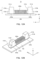
- FIGS. 12A through 12D are views illustrating an antenna apparatus not according to another embodiment in the present invention and an electronic component including the same.
- the core member 500 further includes a first extension forming part 513a disposed on the first core portion 510a and a second extension forming part 513b disposed on the second core portion 510b.
- first extension forming part 513a is disposed on the first core portion 510a in a direction from the third core portion 510c to the first core portion 510a.
- the second extension forming part 513b is disposed on the second core portion 510b in a direction from the third core portion 510c to the second core portion 510b.
- the first and second extension forming parts 513a and 513b are disposed in opposing directions based on the third core portion 510c.
- the core member 500 may have a , , shape, that is, an inverted ' ⁇ ' shape, by way of example.
- the shape of the first and second extension forming parts 513a and 513b is not limited to the examples illustrated in FIGS. 12A through 12D . Therefore, the shape, end surface, and size of the parts may be provided in various manners.
- first and second extension forming parts 513a and 513b do not need to have the same shape as one another. Furthermore, the first and second extension forming parts 513a and 513b do not need to have same distances from the first and second mounting surfaces, respectively, thereto.
- first and second extension forming parts 513a and 513b are disposed on the first and second core portions 510a and 510b so as to obtain a target direction of the magnetic flux.
- FIGS. 12A though 12D illustrate the first and second extension forming parts 513a and 513b to be separate structural elements from the third core portion 510c
- the first and second extension forming parts 513a and 513b may be integral parts of the third core portion 510c.
- an antenna apparatus 20 is mounted on a first substrate 700 through first and second pad parts 520a and 520b, so as to configure an electronic component 10.
- the first substrate 700 is a substrate mounted in an interior of a portable terminal such as a smartphone. Additionally, the substrate includes a plurality of active elements, a plurality passive elements, and ICs which are mounted thereon. However, the types of elements included on the substrate is not limited thereto and thus the substrate may include more or less elements. Furthermore, a PCB is provided as the first substrate 700, but is not limited thereto and any other suitable surface may be provided as the first substrate 700.
- the antenna apparatus 20 includes the core member 500 including the first core portion 510a having the first mounting surface on which the first pad part 520a is disposed, the second core portion 510b having the second mounting surface on which the second pad part 520b is disposed, and the third core portion 510c disposed between the first core portion 510a and the second core portion 510b, and the coil portion 600a wound around the core member 500.
- the first core portion 510a further includes the first end surface 511a opposite to the first mounting surface, and the second core portion 510b includes the second end surface 511b opposite to the second mounting surface.
- the core member 500 includes the first and second end surfaces 511a and 511b through which the magnetic flux enters and exits.
- the first and second pad parts 520a and 520b are formed to extend from one of the surfaces of the first and second extension forming parts 513a and 513b in a direction of the first substrate 700, respectively.
- FIGS. 12A and 12B illustrate the first and second extension forming parts 513a and 513b being disposed over a portion of the first and second pad parts 520a and 520b, this is merely an example and the first and second extension forming parts 513a and 513b can differ in dimension from that of the first and second pad parts 520a and 520b.
- the first and second pad parts 520a and 520b are positioned to be spaced apart from one another so as to perform an SMT on the first substrate 700.
- the antenna apparatus 20 is electrically connected to the first substrate 700 by a soldering scheme in which the first and second pad parts 520a and 520b are disposed on the first substrate 700.
- a coil portion 600a is wound around the third core portion 510c.
- the coil portion 600b is wound around the first and second core portions 510a and 510b.
- the coil portion 600a is wound around the third core portion 510c, and the coil portion 600b is wound around the first and second core portions 510a and 510b.
- FIGS. 12C and 12D illustrate the coil portion 600b being wound and extending from an upper end surface 511a to the third core portion 510c this is merely an example and thus the coil portion 600b may be wound differently.
- FIGS. 12A, 12B and 12D illustrate the coil portion 600a being mostly would around an entire surface of the third core portion 510c, this is merely an example and thus the coil portion 600a may be wound differently around the third core portion 510c.
- the coil portions 600a and 600b transmit and receive data through electromagnetic induction formed based on entry and exit of the magnetic flux. More particularly, the coil portions 600a and 600b are electrically connected to a circuit part mounted on the first substrate 700 through the first and second pad parts 520a and 520b.
- the first substrate 700 includes the circuit part including the NFC chip (not illustrated) disposed thereon.
- the coil portions 600 are electrically connected to the circuit part through the first and second pad parts 520a and 520b.
- the coil portion 600a and 600b perform transmission and reception of data with an external electronic device through electromagnetic induction formed based on the entry and exit of the magnetic flux through the end surfaces 511a and 511b of the respective first and second core portions 510a and 510b.
- the external electronic device includes an antenna capable of transmitting and receiving a signal in the same frequency band as that of the antenna apparatus 20 according to an embodiment.
- the antenna apparatus further includes the second substrate 220 (see FIGS. 8A and 8B ) having the cavity, and the coil portion 600b positioned in the cavity of the second substrate 220 (see FIGS. 8A and 8B ).
- the antenna apparatus 20 includes a chip structure formed by coupling the core member 500 and the second substrate 220 (see FIG. 8A ) to one another, so as to allow for product miniaturization.
- FIGS. 13A and 13B are views illustrating a direction of magnetic flux based on a position in an antenna apparatus not according to an embodiment in the present invention around which the coil portions 200a and 200b (see FIGS. 1 and 6A ) are wound.
- FIGS. 13A and 13B it is seen that strength of the magnetic flux formed around the two first protrusion portions 120a and 120b (see FIG. 1 ) is stronger in the case in which the coil portion 200a (see FIG. 1 ) is wound around the support part 110 (see FIG. 1 ), as compared to the case in which the coil portion 200b (see FIG. 6A ) is wound around the plurality of first protrusion portions 120.
- FIG. 14 is an exploded perspective view illustrating an electronic device not according to another embodiment in the present invention.
- an electronic device includes a cover 30 for an electronic device, the antenna apparatus 20 disposed inwardly of the cover 30 for the electronic device, and the first substrate 400 (see FIG. 3A ).
- the cover 30 for the electronic device is disposed over the electronic device.
- the cover 30 for the electronic device is an external cover.
- the cover 30 for the electronic device is described as the external cover, the cover 30 for the electronic device is not limited thereto.
- a material of the cover 30 for the electronic device may be plastic by way of example but is not limited thereto.
- the antenna apparatus 20 includes the core member 100 having the support part 110, the plurality of first protrusion portions 120 disposed on one surface of the support part 110, and the plurality of second protrusion portions 130 disposed on the other surface of the support part 110, opposite to one surface of the support part 110, and the coil portion 200a wound around the core member 100.
- the plurality of first protrusion portions 120 include the plurality of end surfaces 121a and 121b through which the magnetic flux enters and exits, and the shape and position of the plurality of end surfaces 121a and 121b are not limited as long as the magnetic flux enters and exits there through.
- the plurality of second protrusion portions 130 include the plurality of end surfaces 131a and 131b provided as the mounting surfaces, respectively, and the antenna apparatus 20 is mounted on the first substrate 400 through the first and second pad parts 310 and 320 disposed on the end surfaces 131a and 131b which are provided as the mounting surfaces, respectively.
- the antenna apparatus 20 mounted on the first substrate 400 further includes the first molding part 410 ( FIG. 4A ) disposed between the two first protrusion portions 120a and 120b.
- the antenna apparatus 20 mounted on the first substrate 400 further includes the second molding part 420 ( FIG. 4B ) formed so as to encapsulate the support part 110, the two first protrusion portions 120a and 120b, and the two second protrusion portions 130a and 130b.
- the first substrate 400 includes a circuit part to which the antenna apparatus 20 is connected, and more particularly, includes an NFC chip (not illustrated) electrically connected to the antenna apparatus 20.
- the antenna apparatus 20 is mounted on the first substrate 400 and is disposed inwardly of the cover 30 for the electronic device. Additionally, the antenna apparatus 20 is disposed in a groove 41 formed in an internal cover of the portable terminal, for example, the electronic device. Alternatively, the antenna apparatus 20 is disposed in a battery (not illustrated).
- the coil portion 200a among the components of the antenna apparatus 20 as described above is electrically connected to a circuit part of a body of the portable terminal through the first and second pad parts 310 and 320, and the coil portion 200a is not limited to a particular position as long as the antenna apparatus 20 forms an electromagnetic coupling with the cover 30 for the electronic device.
- the antenna apparatus 20 is disposed in a position of the electronic device at which an electromagnetic wave enters and exits through a portion of the cover 30 for the electronic device.
- the antenna apparatus, and the electronic component and the electronic device including the same are provided by forming the antenna apparatus in the chip shape, whereby an area of the substrate occupied by the antenna apparatus in the case in which the antenna apparatus is mounted thereon is reduced.
- a ferrite sheet formed below the core member to remove the eddy current may not be needed.
- the antenna apparatus is directly mounted on the substrate through the pad parts without an additional substrate mounting structure, miniaturization of the antenna apparatus is achieved. Additionally, a relatively simplified mounting of the antenna apparatus on the substrate is provided.
Landscapes
- Engineering & Computer Science (AREA)
- Computer Networks & Wireless Communication (AREA)
- Health & Medical Sciences (AREA)
- Toxicology (AREA)
- Physics & Mathematics (AREA)
- Electromagnetism (AREA)
- General Health & Medical Sciences (AREA)
- Artificial Intelligence (AREA)
- Computer Vision & Pattern Recognition (AREA)
- General Physics & Mathematics (AREA)
- Theoretical Computer Science (AREA)
- Support Of Aerials (AREA)
- Details Of Aerials (AREA)
- Coils Or Transformers For Communication (AREA)
Claims (6)
- Antennenvorrichtung, umfassend:ein Kernelement (100) aufweisend ein Trägerteil (110), erste Vorsprungsbereiche (120, 120a, 120b), die auf einer Oberfläche des Trägerteils angeordnet sind, zweite Vorsprungsbereiche (130, 130a, 130b), die auf der anderen Oberfläche des Trägerteils, gegenüber der einen Oberfläche des Trägerteils, angeordnet sind; undSpulenbereiche (200a, 200b), die um das Kernelement gewickelt sind,wobei der Spulenbereich (200b) um jeden der ersten Vorsprungsbereiche (120a, 120b) gewickelt ist,wobei die Antennenvorrichtung ferner ein zweites Substrat (220) umfasst, das Hohlräume aufweist, die mit dem Kernelement (100) gekoppelt sind,wobei die Spulenbereiche (200b) so ausgebildet sind, dass sie die Hohlräume umgeben,wobei die ersten Vorsprungsbereiche (120, 120a, 120b) jeweils in den Hohlräumen des zweiten Substrats angeordnet sind, undwobei der Spulenbereich (200b) einen Spulenverbindungsbereich (210) beinhaltet, der die Spulenbereiche (200b) verbindet, und der Spulenverbindungsbereich (210) in dem Hohlraum des zweiten Substrats (220) ausgebildet ist.
- Antennenvorrichtung gemäß Anspruch 1, wobei das Kernelement auf einem ersten Substrat (400) durch Polsterteile befestigt ist, die jeweils auf Befestigungsflächen (131a, 131b, 521a, 521b) der zweiten Vorsprungsbereiche angeordnet sind.
- Antennenvorrichtung gemäß Anspruch 1, wobei die ersten und zweiten Vorsprungsbereiche so auf dem Trägerteil angeordnet sind, dass das Kernelement eine "H"-Form aufweist.
- Antennenvorrichtung gemäß Anspruch 1, wobei die ersten Vorsprungsbereiche Endflächen aufweisen, durch die der Magnetfluss ein- und austritt.
- Antennenvorrichtung gemäß Anspruch 1, wobei eine Länge eines der ersten Vorsprungsbereiche, die aus dem Trägerteil herausragen, von einer Länge eines der zweiten Vorsprungsbereiche, die aus dem Trägerteil herausragen, verschieden ist.
- Vorrichtung gemäß Anspruch 1, wobei das Kernelement einen Winkel von 180° einer Richtung, in der der Magnetfluss in eine der Endflächen des Kernelements eintritt, in Bezug auf eine Richtung, in der der Magnetfluss aus einer der Endflächen des Kernelements austritt, aufweist.
Applications Claiming Priority (3)
| Application Number | Priority Date | Filing Date | Title |
|---|---|---|---|
| KR20140046892 | 2014-04-18 | ||
| KR20140077033 | 2014-06-24 | ||
| KR1020140096722A KR101580401B1 (ko) | 2014-04-18 | 2014-07-29 | 안테나 장치, 이를 갖는 전자 부품 및 전자 기기 |
Publications (2)
| Publication Number | Publication Date |
|---|---|
| EP2933878A1 EP2933878A1 (de) | 2015-10-21 |
| EP2933878B1 true EP2933878B1 (de) | 2024-05-15 |
Family
ID=52814916
Family Applications (1)
| Application Number | Title | Priority Date | Filing Date |
|---|---|---|---|
| EP15163088.6A Active EP2933878B1 (de) | 2014-04-18 | 2015-04-10 | Antennenvorrichtung |
Country Status (3)
| Country | Link |
|---|---|
| US (1) | US9673524B2 (de) |
| EP (1) | EP2933878B1 (de) |
| CN (1) | CN105006627B (de) |
Families Citing this family (5)
| Publication number | Priority date | Publication date | Assignee | Title |
|---|---|---|---|---|
| US9632734B2 (en) * | 2014-12-09 | 2017-04-25 | Zih Corp. | Spindle supported near field communication device |
| KR20170136354A (ko) * | 2016-06-01 | 2017-12-11 | 삼성전기주식회사 | 칩 안테나 |
| US10998613B2 (en) * | 2017-03-23 | 2021-05-04 | Wits Co., Ltd. | Chip antenna |
| KR102088032B1 (ko) * | 2017-08-18 | 2020-03-11 | 주식회사 아모텍 | 안테나 모듈 |
| JP7120602B2 (ja) * | 2018-04-09 | 2022-08-17 | 東京パーツ工業株式会社 | アンテナコイルおよびアンテナ装置 |
Citations (1)
| Publication number | Priority date | Publication date | Assignee | Title |
|---|---|---|---|---|
| US20090256560A1 (en) * | 2005-09-13 | 2009-10-15 | Kunitaka Arimura | Sensor system embedded in metal |
Family Cites Families (16)
| Publication number | Priority date | Publication date | Assignee | Title |
|---|---|---|---|---|
| JP2001337181A (ja) | 2000-03-22 | 2001-12-07 | Mitsubishi Materials Corp | 電波時計用アンテナ |
| CN1623251A (zh) * | 2002-03-05 | 2005-06-01 | 日商·胜美达股份有限公司 | 天线线圈 |
| JP3780995B2 (ja) * | 2002-10-03 | 2006-05-31 | カシオ計算機株式会社 | アンテナ及びアンテナ製造方法 |
| EP1689029B1 (de) | 2003-11-27 | 2016-10-05 | Hitachi Metals, Ltd. | Antenne und funkuhr damit, schlüsselloses eingangssystem und rf-id-system |
| JP2005295473A (ja) * | 2004-04-06 | 2005-10-20 | Toko Inc | アンテナコイル |
| US7295168B2 (en) * | 2004-05-20 | 2007-11-13 | Yonezawa Electric Wire Co., Ltd. | Antenna coil |
| CN101283521B (zh) | 2005-10-14 | 2013-03-13 | 国际商业机器公司 | 电磁感应型rfid标签和访问装置 |
| JP2007306137A (ja) | 2006-05-09 | 2007-11-22 | Sumida Corporation | コイルアンテナの実装方法およびアンテナ装置 |
| JP3957000B1 (ja) | 2006-07-07 | 2007-08-08 | 株式会社村田製作所 | 基板実装用アンテナコイル及びアンテナ装置 |
| JP2010066045A (ja) | 2008-09-09 | 2010-03-25 | Casio Comput Co Ltd | 電波受信装置 |
| US9153855B2 (en) * | 2009-08-28 | 2015-10-06 | Panasonic Intellectual Property Management Co., Ltd. | Antenna, antenna unit, and communication device using them |
| JP2011139245A (ja) | 2009-12-28 | 2011-07-14 | Tdk Corp | アンテナコイル |
| US20110291904A1 (en) | 2010-05-26 | 2011-12-01 | Gareth Conway | Extended magnetic core antenna |
| KR101733806B1 (ko) | 2010-08-05 | 2017-05-08 | 삼성전자주식회사 | 휴대용 단말기 |
| US9696269B2 (en) * | 2012-05-15 | 2017-07-04 | Schlumberger Technology Corporation | NMR analysis of a core sample employing an open permanent magnet removable from a core holder |
| KR101392142B1 (ko) | 2012-08-21 | 2014-05-07 | 주식회사 아모텍 | Nfc 안테나 모듈 |
-
2015
- 2015-04-07 US US14/680,376 patent/US9673524B2/en active Active
- 2015-04-10 EP EP15163088.6A patent/EP2933878B1/de active Active
- 2015-04-17 CN CN201510185241.2A patent/CN105006627B/zh active Active
Patent Citations (1)
| Publication number | Priority date | Publication date | Assignee | Title |
|---|---|---|---|---|
| US20090256560A1 (en) * | 2005-09-13 | 2009-10-15 | Kunitaka Arimura | Sensor system embedded in metal |
Also Published As
| Publication number | Publication date |
|---|---|
| US9673524B2 (en) | 2017-06-06 |
| CN105006627B (zh) | 2018-04-10 |
| CN105006627A (zh) | 2015-10-28 |
| EP2933878A1 (de) | 2015-10-21 |
| US20150303572A1 (en) | 2015-10-22 |
Similar Documents
| Publication | Publication Date | Title |
|---|---|---|
| US9742066B2 (en) | Antenna device and communication terminal apparatus | |
| US9997834B1 (en) | Antenna device and communication terminal apparatus | |
| CN102959800B (zh) | 天线装置以及通信终端装置 | |
| KR101179398B1 (ko) | 무접점 전력 전송 장치 및 이를 구비하는 전자 기기 | |
| US20120038443A1 (en) | Communication terminal | |
| US9779353B2 (en) | Antenna device and communication terminal device | |
| EP2933878B1 (de) | Antennenvorrichtung | |
| KR101580401B1 (ko) | 안테나 장치, 이를 갖는 전자 부품 및 전자 기기 | |
| US20170229777A1 (en) | Antenna structure and antenna apparatus | |
| US10522911B2 (en) | Antenna device, card-type information medium, and communication terminal apparatus | |
| US10122065B2 (en) | Antenna device, card information medium, electronic apparatus, and method for manufacturing antenna device | |
| WO2017033698A1 (ja) | コイル素子、アンテナ装置、カード型情報媒体、無線icデバイスおよび電子機器 | |
| KR20160121362A (ko) | 안테나 장치 및 이를 갖는 전자 기기 | |
| JP2021118528A (ja) | 電子機器及びアンテナ装置 | |
| JP2011199344A (ja) | アンテナ装置 | |
| KR20180002414A (ko) | 안테나 장치 |
Legal Events
| Date | Code | Title | Description |
|---|---|---|---|
| PUAI | Public reference made under article 153(3) epc to a published international application that has entered the european phase |
Free format text: ORIGINAL CODE: 0009012 |
|
| 17P | Request for examination filed |
Effective date: 20150410 |
|
| AK | Designated contracting states |
Kind code of ref document: A1 Designated state(s): AL AT BE BG CH CY CZ DE DK EE ES FI FR GB GR HR HU IE IS IT LI LT LU LV MC MK MT NL NO PL PT RO RS SE SI SK SM TR |
|
| AX | Request for extension of the european patent |
Extension state: BA ME |
|
| RAP1 | Party data changed (applicant data changed or rights of an application transferred) |
Owner name: WITS CO., LTD. |
|
| STAA | Information on the status of an ep patent application or granted ep patent |
Free format text: STATUS: EXAMINATION IS IN PROGRESS |
|
| 17Q | First examination report despatched |
Effective date: 20200115 |
|
| GRAP | Despatch of communication of intention to grant a patent |
Free format text: ORIGINAL CODE: EPIDOSNIGR1 |
|
| STAA | Information on the status of an ep patent application or granted ep patent |
Free format text: STATUS: GRANT OF PATENT IS INTENDED |
|
| INTG | Intention to grant announced |
Effective date: 20231218 |
|
| GRAS | Grant fee paid |
Free format text: ORIGINAL CODE: EPIDOSNIGR3 |
|
| GRAA | (expected) grant |
Free format text: ORIGINAL CODE: 0009210 |
|
| STAA | Information on the status of an ep patent application or granted ep patent |
Free format text: STATUS: THE PATENT HAS BEEN GRANTED |
|
| AK | Designated contracting states |
Kind code of ref document: B1 Designated state(s): AL AT BE BG CH CY CZ DE DK EE ES FI FR GB GR HR HU IE IS IT LI LT LU LV MC MK MT NL NO PL PT RO RS SE SI SK SM TR |
|
| REG | Reference to a national code |
Ref country code: CH Ref legal event code: EP Ref country code: GB Ref legal event code: FG4D |
|
| REG | Reference to a national code |
Ref country code: DE Ref legal event code: R096 Ref document number: 602015088688 Country of ref document: DE |
|
| REG | Reference to a national code |
Ref country code: IE Ref legal event code: FG4D |
|
| REG | Reference to a national code |
Ref country code: LT Ref legal event code: MG9D |
|
| REG | Reference to a national code |
Ref country code: NL Ref legal event code: MP Effective date: 20240515 |
|
| PG25 | Lapsed in a contracting state [announced via postgrant information from national office to epo] |
Ref country code: IS Free format text: LAPSE BECAUSE OF FAILURE TO SUBMIT A TRANSLATION OF THE DESCRIPTION OR TO PAY THE FEE WITHIN THE PRESCRIBED TIME-LIMIT Effective date: 20240915 |
|
| PG25 | Lapsed in a contracting state [announced via postgrant information from national office to epo] |
Ref country code: BG Free format text: LAPSE BECAUSE OF FAILURE TO SUBMIT A TRANSLATION OF THE DESCRIPTION OR TO PAY THE FEE WITHIN THE PRESCRIBED TIME-LIMIT Effective date: 20240515 |
|
| PG25 | Lapsed in a contracting state [announced via postgrant information from national office to epo] |
Ref country code: HR Free format text: LAPSE BECAUSE OF FAILURE TO SUBMIT A TRANSLATION OF THE DESCRIPTION OR TO PAY THE FEE WITHIN THE PRESCRIBED TIME-LIMIT Effective date: 20240515 Ref country code: FI Free format text: LAPSE BECAUSE OF FAILURE TO SUBMIT A TRANSLATION OF THE DESCRIPTION OR TO PAY THE FEE WITHIN THE PRESCRIBED TIME-LIMIT Effective date: 20240515 |
|
| PG25 | Lapsed in a contracting state [announced via postgrant information from national office to epo] |
Ref country code: GR Free format text: LAPSE BECAUSE OF FAILURE TO SUBMIT A TRANSLATION OF THE DESCRIPTION OR TO PAY THE FEE WITHIN THE PRESCRIBED TIME-LIMIT Effective date: 20240816 |
|
| PG25 | Lapsed in a contracting state [announced via postgrant information from national office to epo] |
Ref country code: PT Free format text: LAPSE BECAUSE OF FAILURE TO SUBMIT A TRANSLATION OF THE DESCRIPTION OR TO PAY THE FEE WITHIN THE PRESCRIBED TIME-LIMIT Effective date: 20240916 |
|
| REG | Reference to a national code |
Ref country code: AT Ref legal event code: MK05 Ref document number: 1687664 Country of ref document: AT Kind code of ref document: T Effective date: 20240515 |
|
| PG25 | Lapsed in a contracting state [announced via postgrant information from national office to epo] |
Ref country code: NL Free format text: LAPSE BECAUSE OF FAILURE TO SUBMIT A TRANSLATION OF THE DESCRIPTION OR TO PAY THE FEE WITHIN THE PRESCRIBED TIME-LIMIT Effective date: 20240515 |
|
| PG25 | Lapsed in a contracting state [announced via postgrant information from national office to epo] |
Ref country code: ES Free format text: LAPSE BECAUSE OF FAILURE TO SUBMIT A TRANSLATION OF THE DESCRIPTION OR TO PAY THE FEE WITHIN THE PRESCRIBED TIME-LIMIT Effective date: 20240515 |
|
| PG25 | Lapsed in a contracting state [announced via postgrant information from national office to epo] |
Ref country code: AT Free format text: LAPSE BECAUSE OF FAILURE TO SUBMIT A TRANSLATION OF THE DESCRIPTION OR TO PAY THE FEE WITHIN THE PRESCRIBED TIME-LIMIT Effective date: 20240515 |
|
| PG25 | Lapsed in a contracting state [announced via postgrant information from national office to epo] |
Ref country code: PL Free format text: LAPSE BECAUSE OF FAILURE TO SUBMIT A TRANSLATION OF THE DESCRIPTION OR TO PAY THE FEE WITHIN THE PRESCRIBED TIME-LIMIT Effective date: 20240515 |
|
| PG25 | Lapsed in a contracting state [announced via postgrant information from national office to epo] |
Ref country code: LV Free format text: LAPSE BECAUSE OF FAILURE TO SUBMIT A TRANSLATION OF THE DESCRIPTION OR TO PAY THE FEE WITHIN THE PRESCRIBED TIME-LIMIT Effective date: 20240515 |
|
| PG25 | Lapsed in a contracting state [announced via postgrant information from national office to epo] |
Ref country code: PT Free format text: LAPSE BECAUSE OF FAILURE TO SUBMIT A TRANSLATION OF THE DESCRIPTION OR TO PAY THE FEE WITHIN THE PRESCRIBED TIME-LIMIT Effective date: 20240916 Ref country code: PL Free format text: LAPSE BECAUSE OF FAILURE TO SUBMIT A TRANSLATION OF THE DESCRIPTION OR TO PAY THE FEE WITHIN THE PRESCRIBED TIME-LIMIT Effective date: 20240515 Ref country code: NO Free format text: LAPSE BECAUSE OF FAILURE TO SUBMIT A TRANSLATION OF THE DESCRIPTION OR TO PAY THE FEE WITHIN THE PRESCRIBED TIME-LIMIT Effective date: 20240815 Ref country code: NL Free format text: LAPSE BECAUSE OF FAILURE TO SUBMIT A TRANSLATION OF THE DESCRIPTION OR TO PAY THE FEE WITHIN THE PRESCRIBED TIME-LIMIT Effective date: 20240515 Ref country code: LV Free format text: LAPSE BECAUSE OF FAILURE TO SUBMIT A TRANSLATION OF THE DESCRIPTION OR TO PAY THE FEE WITHIN THE PRESCRIBED TIME-LIMIT Effective date: 20240515 Ref country code: IS Free format text: LAPSE BECAUSE OF FAILURE TO SUBMIT A TRANSLATION OF THE DESCRIPTION OR TO PAY THE FEE WITHIN THE PRESCRIBED TIME-LIMIT Effective date: 20240915 Ref country code: HR Free format text: LAPSE BECAUSE OF FAILURE TO SUBMIT A TRANSLATION OF THE DESCRIPTION OR TO PAY THE FEE WITHIN THE PRESCRIBED TIME-LIMIT Effective date: 20240515 Ref country code: GR Free format text: LAPSE BECAUSE OF FAILURE TO SUBMIT A TRANSLATION OF THE DESCRIPTION OR TO PAY THE FEE WITHIN THE PRESCRIBED TIME-LIMIT Effective date: 20240816 Ref country code: FI Free format text: LAPSE BECAUSE OF FAILURE TO SUBMIT A TRANSLATION OF THE DESCRIPTION OR TO PAY THE FEE WITHIN THE PRESCRIBED TIME-LIMIT Effective date: 20240515 Ref country code: ES Free format text: LAPSE BECAUSE OF FAILURE TO SUBMIT A TRANSLATION OF THE DESCRIPTION OR TO PAY THE FEE WITHIN THE PRESCRIBED TIME-LIMIT Effective date: 20240515 Ref country code: BG Free format text: LAPSE BECAUSE OF FAILURE TO SUBMIT A TRANSLATION OF THE DESCRIPTION OR TO PAY THE FEE WITHIN THE PRESCRIBED TIME-LIMIT Effective date: 20240515 Ref country code: AT Free format text: LAPSE BECAUSE OF FAILURE TO SUBMIT A TRANSLATION OF THE DESCRIPTION OR TO PAY THE FEE WITHIN THE PRESCRIBED TIME-LIMIT Effective date: 20240515 Ref country code: RS Free format text: LAPSE BECAUSE OF FAILURE TO SUBMIT A TRANSLATION OF THE DESCRIPTION OR TO PAY THE FEE WITHIN THE PRESCRIBED TIME-LIMIT Effective date: 20240815 |
|
| PG25 | Lapsed in a contracting state [announced via postgrant information from national office to epo] |
Ref country code: DK Free format text: LAPSE BECAUSE OF FAILURE TO SUBMIT A TRANSLATION OF THE DESCRIPTION OR TO PAY THE FEE WITHIN THE PRESCRIBED TIME-LIMIT Effective date: 20240515 |
|
| PG25 | Lapsed in a contracting state [announced via postgrant information from national office to epo] |
Ref country code: EE Free format text: LAPSE BECAUSE OF FAILURE TO SUBMIT A TRANSLATION OF THE DESCRIPTION OR TO PAY THE FEE WITHIN THE PRESCRIBED TIME-LIMIT Effective date: 20240515 |
|
| PG25 | Lapsed in a contracting state [announced via postgrant information from national office to epo] |
Ref country code: CZ Free format text: LAPSE BECAUSE OF FAILURE TO SUBMIT A TRANSLATION OF THE DESCRIPTION OR TO PAY THE FEE WITHIN THE PRESCRIBED TIME-LIMIT Effective date: 20240515 |
|
| PG25 | Lapsed in a contracting state [announced via postgrant information from national office to epo] |
Ref country code: RO Free format text: LAPSE BECAUSE OF FAILURE TO SUBMIT A TRANSLATION OF THE DESCRIPTION OR TO PAY THE FEE WITHIN THE PRESCRIBED TIME-LIMIT Effective date: 20240515 Ref country code: SK Free format text: LAPSE BECAUSE OF FAILURE TO SUBMIT A TRANSLATION OF THE DESCRIPTION OR TO PAY THE FEE WITHIN THE PRESCRIBED TIME-LIMIT Effective date: 20240515 |
|
| PG25 | Lapsed in a contracting state [announced via postgrant information from national office to epo] |
Ref country code: SM Free format text: LAPSE BECAUSE OF FAILURE TO SUBMIT A TRANSLATION OF THE DESCRIPTION OR TO PAY THE FEE WITHIN THE PRESCRIBED TIME-LIMIT Effective date: 20240515 |
|
| PG25 | Lapsed in a contracting state [announced via postgrant information from national office to epo] |
Ref country code: SM Free format text: LAPSE BECAUSE OF FAILURE TO SUBMIT A TRANSLATION OF THE DESCRIPTION OR TO PAY THE FEE WITHIN THE PRESCRIBED TIME-LIMIT Effective date: 20240515 Ref country code: SK Free format text: LAPSE BECAUSE OF FAILURE TO SUBMIT A TRANSLATION OF THE DESCRIPTION OR TO PAY THE FEE WITHIN THE PRESCRIBED TIME-LIMIT Effective date: 20240515 Ref country code: RO Free format text: LAPSE BECAUSE OF FAILURE TO SUBMIT A TRANSLATION OF THE DESCRIPTION OR TO PAY THE FEE WITHIN THE PRESCRIBED TIME-LIMIT Effective date: 20240515 Ref country code: EE Free format text: LAPSE BECAUSE OF FAILURE TO SUBMIT A TRANSLATION OF THE DESCRIPTION OR TO PAY THE FEE WITHIN THE PRESCRIBED TIME-LIMIT Effective date: 20240515 Ref country code: DK Free format text: LAPSE BECAUSE OF FAILURE TO SUBMIT A TRANSLATION OF THE DESCRIPTION OR TO PAY THE FEE WITHIN THE PRESCRIBED TIME-LIMIT Effective date: 20240515 Ref country code: CZ Free format text: LAPSE BECAUSE OF FAILURE TO SUBMIT A TRANSLATION OF THE DESCRIPTION OR TO PAY THE FEE WITHIN THE PRESCRIBED TIME-LIMIT Effective date: 20240515 |
|
| PG25 | Lapsed in a contracting state [announced via postgrant information from national office to epo] |
Ref country code: IT Free format text: LAPSE BECAUSE OF FAILURE TO SUBMIT A TRANSLATION OF THE DESCRIPTION OR TO PAY THE FEE WITHIN THE PRESCRIBED TIME-LIMIT Effective date: 20240515 |
|
| REG | Reference to a national code |
Ref country code: DE Ref legal event code: R097 Ref document number: 602015088688 Country of ref document: DE |
|
| PLBE | No opposition filed within time limit |
Free format text: ORIGINAL CODE: 0009261 |
|
| STAA | Information on the status of an ep patent application or granted ep patent |
Free format text: STATUS: NO OPPOSITION FILED WITHIN TIME LIMIT |
|
| 26N | No opposition filed |
Effective date: 20250218 |
|
| PG25 | Lapsed in a contracting state [announced via postgrant information from national office to epo] |
Ref country code: SI Free format text: LAPSE BECAUSE OF FAILURE TO SUBMIT A TRANSLATION OF THE DESCRIPTION OR TO PAY THE FEE WITHIN THE PRESCRIBED TIME-LIMIT Effective date: 20240515 |
|
| PGFP | Annual fee paid to national office [announced via postgrant information from national office to epo] |
Ref country code: FR Payment date: 20250321 Year of fee payment: 11 |
|
| PGFP | Annual fee paid to national office [announced via postgrant information from national office to epo] |
Ref country code: GB Payment date: 20250320 Year of fee payment: 11 |
|
| PGFP | Annual fee paid to national office [announced via postgrant information from national office to epo] |
Ref country code: DE Payment date: 20250320 Year of fee payment: 11 |
|
| PG25 | Lapsed in a contracting state [announced via postgrant information from national office to epo] |
Ref country code: SE Free format text: LAPSE BECAUSE OF FAILURE TO SUBMIT A TRANSLATION OF THE DESCRIPTION OR TO PAY THE FEE WITHIN THE PRESCRIBED TIME-LIMIT Effective date: 20240515 |
|
| REG | Reference to a national code |
Ref country code: CH Ref legal event code: H13 Free format text: ST27 STATUS EVENT CODE: U-0-0-H10-H13 (AS PROVIDED BY THE NATIONAL OFFICE) Effective date: 20251125 |
|
| PG25 | Lapsed in a contracting state [announced via postgrant information from national office to epo] |
Ref country code: LU Free format text: LAPSE BECAUSE OF NON-PAYMENT OF DUE FEES Effective date: 20250410 |
|
| PG25 | Lapsed in a contracting state [announced via postgrant information from national office to epo] |
Ref country code: MC Free format text: LAPSE BECAUSE OF FAILURE TO SUBMIT A TRANSLATION OF THE DESCRIPTION OR TO PAY THE FEE WITHIN THE PRESCRIBED TIME-LIMIT Effective date: 20240515 |
|
| REG | Reference to a national code |
Ref country code: BE Ref legal event code: MM Effective date: 20250430 |
|
| PG25 | Lapsed in a contracting state [announced via postgrant information from national office to epo] |
Ref country code: BE Free format text: LAPSE BECAUSE OF NON-PAYMENT OF DUE FEES Effective date: 20250430 |
|
| PG25 | Lapsed in a contracting state [announced via postgrant information from national office to epo] |
Ref country code: CH Free format text: LAPSE BECAUSE OF NON-PAYMENT OF DUE FEES Effective date: 20250430 |
|
| PG25 | Lapsed in a contracting state [announced via postgrant information from national office to epo] |
Ref country code: IE Free format text: LAPSE BECAUSE OF NON-PAYMENT OF DUE FEES Effective date: 20250410 |