EP2936081B1 - Sensor zur ermittlung einer prozessgrösse eines mediums - Google Patents
Sensor zur ermittlung einer prozessgrösse eines mediums Download PDFInfo
- Publication number
- EP2936081B1 EP2936081B1 EP13811437.6A EP13811437A EP2936081B1 EP 2936081 B1 EP2936081 B1 EP 2936081B1 EP 13811437 A EP13811437 A EP 13811437A EP 2936081 B1 EP2936081 B1 EP 2936081B1
- Authority
- EP
- European Patent Office
- Prior art keywords
- sensor
- layer
- dielectric layer
- heating structure
- dielectric
- Prior art date
- Legal status (The legal status is an assumption and is not a legal conclusion. Google has not performed a legal analysis and makes no representation as to the accuracy of the status listed.)
- Active
Links
Images
Classifications
-
- G—PHYSICS
- G01—MEASURING; TESTING
- G01F—MEASURING VOLUME, VOLUME FLOW, MASS FLOW OR LIQUID LEVEL; METERING BY VOLUME
- G01F1/00—Measuring the volume flow or mass flow of fluid or fluent solid material wherein the fluid passes through a meter in a continuous flow
- G01F1/68—Measuring the volume flow or mass flow of fluid or fluent solid material wherein the fluid passes through a meter in a continuous flow by using thermal effects
- G01F1/684—Structural arrangements; Mounting of elements, e.g. in relation to fluid flow
- G01F1/688—Structural arrangements; Mounting of elements, e.g. in relation to fluid flow using a particular type of heating, cooling or sensing element
-
- G—PHYSICS
- G01—MEASURING; TESTING
- G01F—MEASURING VOLUME, VOLUME FLOW, MASS FLOW OR LIQUID LEVEL; METERING BY VOLUME
- G01F1/00—Measuring the volume flow or mass flow of fluid or fluent solid material wherein the fluid passes through a meter in a continuous flow
- G01F1/68—Measuring the volume flow or mass flow of fluid or fluent solid material wherein the fluid passes through a meter in a continuous flow by using thermal effects
- G01F1/684—Structural arrangements; Mounting of elements, e.g. in relation to fluid flow
- G01F1/6845—Micromachined devices
-
- G—PHYSICS
- G01—MEASURING; TESTING
- G01F—MEASURING VOLUME, VOLUME FLOW, MASS FLOW OR LIQUID LEVEL; METERING BY VOLUME
- G01F1/00—Measuring the volume flow or mass flow of fluid or fluent solid material wherein the fluid passes through a meter in a continuous flow
- G01F1/68—Measuring the volume flow or mass flow of fluid or fluent solid material wherein the fluid passes through a meter in a continuous flow by using thermal effects
- G01F1/684—Structural arrangements; Mounting of elements, e.g. in relation to fluid flow
- G01F1/688—Structural arrangements; Mounting of elements, e.g. in relation to fluid flow using a particular type of heating, cooling or sensing element
- G01F1/69—Structural arrangements; Mounting of elements, e.g. in relation to fluid flow using a particular type of heating, cooling or sensing element of resistive type
- G01F1/692—Thin-film arrangements
Definitions
- the invention relates to a sensor that is used to determine at least one process variable of a medium.
- the process variable is, for example, the throughput of a medium, the gas concentration of a gas in a gas mixture or the thermal properties of a gas.
- Thermal flow sensors are already known from the prior art, in which at least one heating element and at least one temperature sensor element are applied to a substrate. These thermal flow sensors are typically fabricated on ceramic, glass, or silicon substrates.
- the heating element must be thermally well decoupled from the temperature sensor element in order to be able to carry out a measurement of the flowing medium that is as sensitive, fast and precise as possible.
- the thermal mass in the area of the flow-sensitive layer ie in the area of the heating element and the temperature sensor element, is kept as low as possible.
- membranes are implemented in this area in order to reduce the bulk or substrate mass and the associated thermal mass.
- flow sensors implemented in this way have the disadvantage that relatively thick substrates have to be used in order to be able to ensure the mechanical stability of the entire sensor.
- JP 2007 017263 A discloses several exemplary embodiments of a thermal flow sensor having a metal substrate and in which the heating elements and temperature sensing elements are curved or domed.
- the curvatures are realized by a membrane, which bends into the desired shape through tension.
- the JP 2011 016173 A discloses a thermal flow sensor with a silicon substrate in which the heating elements are mounted on a membrane which is stretched over a cavity.
- the DE 199 41 420 A1 discloses a temperature sensor having a metallic substrate on which a metallic etch stop layer and an electrically insulating layer are upset.
- the substrate is etched free up to the etch stop layer in an etching process, so that a membrane consisting of two layers - the etch stop layer and the electrically insulating layer - is created.
- the U.S. 5,291,781 A discloses a thermal flow sensor having a metallic substrate with a recess fully penetrating the substrate. A membrane completely covers the recess. Several heating elements are arranged on the membrane, which are thermally decoupled from one another by slots inserted in the membrane.
- the EP 2 348 292 A1 discloses a semiconductor sensor which has a substrate with a recess and a membrane covering the recess, wherein the membrane consists of a first and a second layer to compensate for thermal stress.
- the sensor also has two heating elements applied to the membrane, which are each arranged partially above the recess and above the substrate.
- the object of the invention is therefore to propose a sensor that generates the least possible turbulence when it is inserted into the place of use and at the same time has a high mechanical stability, as well as a method for producing such a sensor.
- a metallic substrate which serves as a carrier and can be made particularly thin, preferably a thickness in the range of 50-250 ⁇ m (micrometers), but particularly preferably a thickness less than 200 ⁇ m, by reducing the overall height of the
- less impairment of the environment e.g. eddy formation
- it can be used in a flow channel without significant turbulence occurring.
- it is also desirable to obtain a sensitive and fast sensor, particularly in the case of a flow sensor. This requires, among other things, a thermal decoupling of the heating structure from the temperature sensor element and a reduction in the thermal mass.
- the at least one heating structure formed on a membrane.
- the metallic substrate is structured, typically by means of industrially suitable etching processes, in such a way that it has a cutout through which Z the first dielectric layer Z forms a membrane.
- the first area is essentially the area above the recess made in the metallic substrate, with the first area relating in particular to the membrane and the layers and/or structures arranged above the membrane.
- assigned to the first area is also to be understood as meaning that the corresponding element is arranged outside this area, this element interacting via the medium with at least one element which is formed within the first area.
- a metal is used as the substrate in order to achieve the reduction in the overall height of the sensor, since metals offer the advantage that they have high mechanical stability even with very small thicknesses and, moreover, industrially suitable etching processes are used for their structuring can become. Furthermore, metallic substrates can be coated with materials that are not influenced by the process for structuring the metallic substrate, wherein the materials applied to the metallic substrate in the form of a layer can in turn be provided with functional metal structures. Compared to the thermal flow sensors known from the prior art, the use of a metal substrate offers the advantage that metal, in contrast to ceramic substrates, can be structured.
- a first dielectric layer is applied to the metallic substrate.
- a large number of materials such as polyimide, parylene, other plastic layers, metal oxides, silicon oxide, silicon nitride, silicon carbide, glasses etc. can be used as the dielectric layer.
- An advantageous embodiment of the sensor provides that the first dielectric layer has a lower thermal conductivity than the metallic substrate. In this way, the thermal coupling between the heating structure formed on the first dielectric layer and the dielectric layer can be achieved, which in turn leads to a better heat coupling into the medium or the layers above it.
- the protective layer is designed either as a second dielectric layer or as a layered composite, the layered composite comprising at least a second dielectric layer and a third, preferably dielectric, layer.
- the layered composite is designed such that the second dielectric layer covers at least the at least one heating structure and the at least one temperature sensor element and the third, preferably dielectric, layer at least partially covers the second dielectric layer. Due to the essentially flat coating of the at least one heating structure and the at least one temperature sensor element, standard processes that are based in semiconductor technology and already established in micromechanics can be used and a particularly cost-effective realization of the sensors is made possible.
- the layered composite is designed such that the second dielectric layer covers at least the lateral areas of the at least one heating structure and the surfaces of the at least one heating structure and the at least one temperature sensor element are covered by the third, preferably dielectric, layer.
- the thermal conductivity of the third, preferably dielectric, layer is particularly preferably better than that of the first and/or second dielectric layer. Due to the selective layer structure, a particularly good heat transfer can be realized between the heating structure and the medium, as well as between the temperature sensor element and the medium.
- the coefficient of thermal expansion of the first dielectric layer is selected in such a way that a tensile stress is formed on the membrane.
- the tensile stress acting on the membrane can prevent the membrane from buckling, which in turn ensures that the membrane surface is particularly smooth.
- the thermal expansion coefficient of the second dielectric layer is in the range of the thermal expansion coefficient of the first dielectric layer, in particular the deviation of the thermal expansion coefficients from one another is less than 20%, preferably less than 10%.
- the first dielectric layer and the third, preferably dielectric, layer comprises polyimide, Kapton and/or Parylene and/or the at least one heating structure and the at least one temperature sensor element platinum or nickel or a nickel compound.
- the object is achieved by a method for producing a sensor as is described in at least one of the previous embodiments, the sensor being held together in a composite comprising a large number of sensors during the production process, the metallic substrate of the sensors being used for this purpose is connected to the metallic substrate of the adjacent sensor via at least one web in each case, and the at least one web is destroyed and the sensor is detached from the assembly in order to isolate the sensor.
- An advantageous embodiment of the method provides that the at least one path is produced by an etching process using a masking layer.
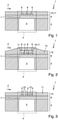
- the sensor 1 shows a cross section of a first embodiment of a generic sensor 1.
- the sensor 1 has a metallic substrate 3 made of stainless steel.
- a first dielectric layer 6, which essentially comprises polyimide, is applied to this metallic substrate 3.
- a cutout 5 is introduced into the metallic substrate 3 by means of industrially suitable manufacturing processes, in particular etching processes.
- the first dielectric layer 6 forms a membrane 7 by introducing the cutout 5 into the metallic substrate 3 .
- the recess 5 and the first dielectric layer 6 located above the recess 5 form a first area 4 off.
- a heating structure 8 formed on the first dielectric layer 6 is arranged within the first region 4 .
- At least one temperature sensor element 9 is applied to the first dielectric layer 6 next to the heating structure 8 .
- two temperature sensor elements 9 are realized. These temperature sensor elements 9 are arranged at a distance from the heating structure 8 .
- at least one temperature sensor element 9 is arranged outside of the first area 4, but can be assigned to the first area 4 in terms of function in such a way that there is an interaction or relationship between the heating structure 8 arranged within the first area 4 and the temperature sensor element 9.
- the temperature of a medium 2 which is heated by the heating structure 8 arranged within the first area 4 can be detected by means of the temperature sensor element 9 arranged outside of the first area 4 .
- Both the heating structure 8 and the temperature sensor elements 9 are made of platinum.
- at least one protective layer 10 is provided, which covers the heating structure 8 and the two temperature sensor elements 9. in the in figure 1
- the protective layer comprises only a second, preferably dielectric, layer 11, which is applied over a large area.
- the heater structure can also be made of a material with a low temperature coefficient of resistance (TCR), such as nickel-chromium or nickel-chromium with other additives for targeted adjustment of the TCR.
- TCR temperature coefficient of resistance
- the heating structure 8 and the temperature sensor element 9 can be made of any metal or metal compound that exhibits a TCR, for example tantalum or nickel.
- the material of the first dielectric layer 6 is selected in such a way that due to the thermal expansion coefficient, there is a tensile stress on the membrane 7, at least after the complete processing or production of the sensor 1. This offers the advantage that a non-curved shape of the membrane 7 is achieved, which ensures that the membrane 7 forms a surface that is as smooth as possible.
- Figure 2 and Figure 3 show cross-sections of further configurations of the generic sensor 1, the configuration essentially according to in figure 1 Sensor 1 shown corresponds, only the protective layer 10 is formed differently in an advantageous manner.
- the at least one protective layer 10 is designed as a layered composite 11, 13, which comprises a second and third layer 11, 13, the second and third layer 11, 13 preferably also being dielectric represent layers.
- the configuration shown offers the advantage that the use of a layered composite 11, 13, which consists of at least a second and a third layer 11, 13, allows the layered composite to be adjusted according to the medium 2 or the aggressiveness of the medium 2 and the heating structure 8 and/or temperature sensor element 9 can thus be specifically protected from the respective medium 2.
- the coefficient of thermal expansion of the second, preferably dielectric, layer 11 is in the range of the coefficient of thermal expansion of the first dielectric layer 6 .
- the second layer 11 which preferably represents a dielectric layer, is a metal oxide layer that covers at least the heating structure 8 and the temperature sensor element 9 locally.
- This second layer 11 is in turn covered with a third layer 13 applied over the entire surface, preferably also a dielectric layer, for example a polymer such as parylene.
- the heating structure 8 and/or the temperature sensor element 9 can be protected against specific media, in particular aggressive media 2 .
- Aggressive media are e.g. acidic or basic media or condensing humidity.
- the heating structure 8 and/or the temperature sensor element 9 can be protected from specific media 2, but this method has the disadvantage that there is less thermal coupling between the heating structure 8 and the medium 2 or the temperature sensor element 9 and the medium 2 arises and thus a fast response time of the sensor 1 is difficult to achieve.
- FIG 3 A further alternative embodiment of the generic sensor 1 is shown, in which the layered composite is designed in such a way that the second, preferably dielectric, layer 11 is applied flatly to the first dielectric layer 6, with the second layer 11 at least covering the lateral areas or side walls of the at least one heating structure 8 and/or of the temperature sensor element 9 and the surfaces, i.e. the side or area facing the medium 2, of the at least one heating structure 8 and of the at least one temperature sensor element 9 are covered by a third, preferably again dielectric, layer 13 .
- the thermal conductivity of the third layer 13 is better than that of the first and/or second layer 6, 11. In this way, an improved thermal coupling between the medium 2 and the heating structure 8 and the temperature sensor element 9 and the medium 2 can be realized by means of the third layer 13 in order to achieve the fastest possible response time of the sensor 1.
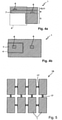
- FIG 4 shows an embodiment of the sensor 1 according to the invention figure 4 a) a side view, which is incorrect and is not attributed to the sensor according to the invention.
- Figure 4 b) shows a top view of the sensor 1 according to the invention.
- a dielectric layer 6 is applied to the metallic substrate 3, which is made of stainless steel, and forms a membrane 7 in the first area 4 of the recess 5, the first area 4 in turn being on the membrane 7 and the layers arranged above the membrane 7 and/or related elements.
- the at least one heating structure 8 for heating the medium 2 is formed within this first region 4 .
- the temperature sensor element 9 is arranged outside of the first region 4, but can be assigned to the first region 4 in that it interacts with elements and/or structures that are arranged within the first region 4 in such a way that a medium 2, in particular a flowing medium 2 is heated at the heating structure 8 located within the first region 4 and the temperature of the medium 2 at the temperature sensor element 9 located outside of the first region 4 is detected.
- This protective layer 10 is in the in Figure 4a sensor shown in the form of a single second layer 11 configured.
- the protective layer 10 it is also conceivable, in particular for specific fields of application of the sensor 1, to form the protective layer 10 as a layered composite 12 which comprises at least two further layers, with the two further layers preferably being formed as dielectric layers.
- figure 5 shows a schematic representation of a composite 16, which includes a plurality of sensors 1 and is used to produce a sensor 1 according to the invention.
- a large number of sensors 1 are held together by a composite 16 during the production process, with the metallic substrate 3 of the sensors 1 being connected to this by at least one web 17 is connected to the metallic substrate 3 of the adjacent sensor 1, and in order to isolate a sensor 1, the webs 17 adjoining this sensor are destroyed and the sensor 1 is thus separated from the composite 16.
Landscapes
- Physics & Mathematics (AREA)
- Fluid Mechanics (AREA)
- General Physics & Mathematics (AREA)
- Measuring Volume Flow (AREA)
Description
- Die Erfindung bezieht sich auf einen Sensor, der zur Ermittlung mindestens einer Prozessgröße eines Mediums dient. Bei der Prozessgröße handelt es sich beispielsweise um den Durchsatz eines Mediums, die Gaskonzentration eines Gases in einem Gasgemisch oder auch die thermischen Eigenschaften eines Gases.
- Aus dem Stand der Technik sind bereits thermische Strömungssensoren bekannt geworden, bei denen auf einem Substrat zumindest ein Heizelement und zumindest ein Temperatursensorelement aufgebracht ist. Diese thermischen Strömungssensoren werden typischerweise auf Keramik-, Glas- oder Siliziumsubstraten hergestellt.
- Ebenfalls ist aus dem Stand der Technik bekannt geworden, dass das Heizelement von dem Temperatursensorelement gut wärmetechnisch entkoppelt sein muss, umso eine möglichst sensitive, schnelle und präzise Messung des strömenden Mediums vornehmen zu können. Um diese wärmetechnische Entkopplung zu realisieren, wird die thermische Masse im Bereich der strömungssensitiven Schicht, also im Bereich des Heizelementes und des Temperatursensorelementes, möglichst gering gehalten. Hierfür werden in diesem Bereich Membrane realisiert, umso die Bulk- bzw. Substratmasse und damit einhergehend auch die thermische Masse zu reduzieren. Derartig realisierte Strömungssensoren weisen jedoch den Nachteil auf, dass relativ dicke Substrate eingesetzt werden müssen, um die mechanische Stabilität des gesamten Sensors sicherstellen zu können. Dies führt allerdings dazu, dass nach dem Einbringen dieser Strömungssensoren in die dafür vorgesehene Anwendung es zu ungünstigen Verwirbelungen kommt, welche wiederum zu unpräzisen, möglicherweise sogar gänzlich falschen Messwerten führen.
- In der
JP 2007 017263 A - Die
JP 2011 016173 A - Die
DE 199 41 420 A1 offenbart einen Temperatursensor mit einem metallischen Substrat auf dem eine metallische Ätzstoppschicht und eine elektrisch isolierende Schicht aufgebracht sind. Das Substrat wird durch einen Ätzprozess bis an die Ätzstoppschicht freigeätzt, sodass im Anschluss eine Membran aus zwei Schichten - der Ätzstoppschicht und der elektrisch isolierenden Schicht - entsteht. - Die
US 5 291 781 A offenbart einen thermischen Strömungssensor, welcher ein metallisches Substrat mit einer das Substrat vollständig durchdringenden Aussparung aufweist. Eine Membran bedeckt die Aussparung vollständig. Auf der Membran sind mehrere Heizelemente angeordnet, welche durch in die Membran eingefügte Schlitze thermische voneinander entkoppelt werden. - Die
EP 2 348 292 A1 offenbart einen Halbleitersensor welcher ein Substrat mit einer Aussparung und eine die Aussparung bedeckende Membran aufweist, wobei die Membran zur Kompensation von thermischem Stress aus einer ersten und einer zweiten Schicht besteht. Der Sensor weist weiterhin zwei auf der Membran aufgebrachte Heizelemente auf, die jeweils teilweise über der Aussparung und über dem Substrat angeordnet sind. - Somit ist die Aufgabe der Erfindung einen Sensor, der beim Einsetzen in den Einsatzort möglichst geringe Verwirbelungen erzeugt und gleichzeitig eine hohe mechanische Stabilität aufweist, sowie ein Verfahren zur Herstellung eines solchen Sensors vorzuschlagen.
- Diese Aufgabe wird durch einen Sensor gemäß Anspruch 1 und ein Verfahren gemäß Anspruch 10 gelöst.
- Durch den Einsatz eines metallischen Substrates, welches als Träger dient und besonders dünn ausgeführt werden kann, vorzugsweise eine Dicke im Bereich von 50-250 µm (Mikrometern), besonders bevorzugt jedoch eine Dicke weniger als 200 µm aufweist, kann durch die Reduzierung der Bauhöhe des Sensors bei der Integration in den dafür vorgesehenen Einsatzort eine geringere Beeinträchtigung der Umgebung, bspw. Wirbelbildung, realisiert werden, umso ein noch exakteres bzw. genaueres Messergebnis mittels des Sensors zu erhalten. So kann beispielsweise in dem Fall, dass es sich um einen Strömungssensor handelt, dieser in einen Strömungskanal eingesetzt werden, ohne dass es zu wesentlichen Verwirbelungen kommt. Neben einer möglichst geringen Beeinflussung der Umgebung ist es ebenfalls wünschenswert, einen sensitiven und schnellen Sensor zu erhalten, insbesondere auch bei einem Strömungssensor. Hierzu sind unter anderem eine wärmetechnische Entkopplung der Heizstruktur von dem Temperatursensorelement sowie eine Reduzierung der thermischen Masse nötig. Zur Reduzierung der thermischen Masse wird die zumindest eine Heizstruktur auf einer Membran ausgebildet.
- Hierzu wird, typischerweise mittels industriell tauglichen Ätzverfahren, das metallische Substrat derartig strukturiert, dass es eine Aussparung aufweist, durch Z die Z die erste dielektrische Schicht Z eine Membran ausbildet.
- Im Sinne der vorliegenden Erfindung wird als erster Bereich im Wesentlichen der Bereich oberhalb der in das metallische Substrat eingebrachten Aussparung angesehen, wobei sich der erste Bereich insbesondere auf die Membran sowie die über der Membran angeordneten Schichten und/oder Strukturen bezieht.
- Weiter ist erfindungsgemäß unter dem ersten Bereich zugeordnet zu verstehen, dass das entsprechende Element außerhalb dieses Bereiches angeordnet ist, wobei dieses Element über das Medium in Wechselwirkung mit zumindest einem Element, welches innerhalb des ersten Bereiches ausgebildet ist, steht.
- Erfindungsgemäß wird ein Metall als Substrat verwendet, um so die Reduzierung der Bauhöhe des Sensors zu realisieren, da Metalle den Vorteil bieten, dass sie auch bei sehr geringen Stärken bzw. Dicken eine hohe mechanische Stabilität aufweisen und darüber hinaus industriell taugliche Ätzverfahren zu ihrer Strukturierung angewendet werden können. Weiter können metallische Substrate mit Materialien beschichtet werden, die durch den Prozess zur Strukturierung des metallischen Substrates nicht beeinflusst werden, wobei die auf das metallische Substrat in Form einer Schicht aufgebrachten Materialien wiederum mit funktionellen Metallstrukturen versehen werden können. Gegenüber den aus dem Stand der Technik bekannten thermischen Strömungssensoren, bietet die Verwendung eines Metall-Substrates den Vorteil, dass sich Metall, im Gegensatz zu keramischen Substraten, strukturieren lässt.
- Um eine elektrische Verbindung zwischen der zumindest einen Heizstruktur und dem zumindest einen Temperatursensorelement zu verhindern, ist auf dem metallischen Substrat eine erste dielektrische Schicht aufgebracht. Als dielektrische Schicht kommen prinzipiell eine Vielzahl von Materialien, wie bspw. Polyimid, Parylene, weitere Kunststoffschichten, Metalloxide, Siliziumoxid, Siliziumnitrid, Siliziumcarbid, Gläser etc., einsetzbar.
- Eine vorteilhafte Ausgestaltung des Sensors sieht vor, dass die erste dielektrische Schicht eine geringere thermische Leitfähigkeit als das metallische Substrat aufweist. Auf diese Weise kann die Wärmekopplung zwischen der auf der ersten dielektrischen Schicht ausgebildeten Heizstruktur und der dielektrischen Schicht erzielt werden, was wiederum dazu führt, dass eine bessere Wärmekopplung ins Medium bzw. die darüber liegenden Schichten stattfindet.
- Eine weiter vorteilhafte Ausgestaltung des Sensors sieht vor, dass die Schutzschicht entweder als eine zweite dielektrische Schicht oder als ein Schichtverbund ausgebildet ist, wobei der Schichtverbund zumindest eine zweite dielektrischen Schicht und eine dritte, vorzugsweise dielektrische, Schicht umfasst. Insbesondere ist der Schichtverbund derartig ausgestaltet, dass die zweite dielektrische Schicht zumindest die mindestens eine Heizstruktur und das mindestens eine Temperatursensorelement bedeckt und die dritte, vorzugsweise dielektrische, Schicht die zweite dielektrische Schicht zumindest teilweise bedeckt. Durch die im Wesentlichen flächige Beschichtung der mindestens einen Heizstruktur und des mindestens einen Temperatursensorelementes, können Standard-Prozesse, die in der Halbleitertechnik angesiedelte und in der Mikromechanik bereits etablierte sind, verwendet werden und eine besonders kostengünstige Realisierung der Sensoren ermöglicht werden.
- Alternativ ist der Schichtverbund derartig ausgestaltet, dass die zweite dielektrische Schicht zumindest die seitlichen Bereiche der zumindest einen Heizstruktur bedeckt und die Oberflächen der zumindest einen Heizstruktur und des zumindest einen Temperatursensorelementes von der dritten, vorzugsweise dielektrischen, Schicht bedeckt wird. Besonders bevorzugt ist die thermische Leitfähigkeit der dritten, vorzugweise dielektrischen, Schicht besser als die der ersten und/oder zweiten dielektrischen Schicht. Durch den selektiven Schichtaufbau, lässt sich ein besonders guter Wärmeübergang, zwischen der Heizstruktur und dem Medium, sowie dem Temperatursensorelement und dem Medium, realisieren.
- Gemäß einer Weiterbildung des erfindungsgemäßen Sensors ist der thermische Ausdehnungskoeffizient der ersten dielektrischen Schicht derartig gewählt, dass eine Zugspannung auf der Membran ausgebildet wird. Durch die Zugspannung, welche auf die Membran einwirkt, kann eine Aufwölbung (engl.: "buckling") der Membran verhindert werden, die wiederum dafür sorgt, dass eine besonders glatte Membranoberfläche ausgebildet wird.
- Gemäß einer weiteren Weiterbildung des erfindungsgemäßen Sensors, liegt der thermische Ausdehnungskoeffizient der zweiten dielektrischen Schicht im Bereich des thermischen Ausdehnungskoeffizienten der ersten dielektrischen Schicht, insbesondere ist die Abweichung der thermischen Ausdehnungskoeffizienten zueinander kleiner als 20%, vorzugsweise kleiner als 10%.
- Eine letzte Weiterbildung des erfindungsgemäßen Sensors sieht vor, dass die erste dielektrische Schicht und die dritte, vorzugsweise dielektrische, Schicht Polyimid, Kapton und/oder Parylene und/oder die zumindest eine Heizstruktur und das zumindest eine Temperatursensorelement Platin oder Nickel oder eine Nickelverbindung umfasst.
- Hinsichtlich des Verfahrens wird die Aufgabe durch ein Verfahren zum Herstellen eines Sensors wie er zumindest in einem der vorherigen Ausführungsformen beschrieben ist gelöst, wobei der Sensor in einem aus einer Vielzahl von Sensoren umfassenden Verbund während des Herstellungsprozesses zusammengehalten wird, wobei hierfür das metallische Substrat der Sensoren über jeweils mindestens einen Steg mit dem metallischen Substrat des benachbarten Sensors verbunden ist und wobei zur Vereinzelung des Sensors der mindestens eine Steg zerstört und der Sensor aus dem Verbund herausgelöst wird.
- Eine vorteilhafte Ausgestaltung des Verfahrens sieht vor, dass der mindestens eine Pfad durch einen Ätzprozess mittels einer Maskierungsschicht hergestellt wird.
- Die Erfindung wird anhand der nachfolgenden Zeichnungen näher erläutert. Es zeigt:
- Fig. 1:
- einen Querschnitt einer Ausgestaltung eines gattungsgemäßen Sensors,
- Fig. 2:
- einen Querschnitt einer weiteren Ausgestaltung des gattungsgemäßen Sensors,
- Fig. 3:
- einen Querschnitt einer weiteren Ausgestaltung des gattungsgemäßen Sensors,
- Fig. 4:
- eine Ausgestaltung des erfindungsgemäßen Sensors, und
- Fig. 5:
- eine schematische Darstellung eines Verbundes, welcher eine Vielzahl von
- Sensoren umfasst und Z zum Herstellen eines erfindungsgemäßen Sensors dient
-
Fig. 1 zeigt einen Querschnitt einer ersten Ausgestaltung eines gattungsgemäßen Sensors 1. Hierbei weist der Sensor 1 ein metallisches Substrat 3 aus Edelstahl auf. Auf diesem metallischen Substrat 3 ist eine erste dielektrische Schicht 6, die im Wesentlichen Polyimid umfasst, aufgebracht. Mittels industriell tauglichen Fertigungsverfahren, insbesondere Ätzverfahren, ist in das metallische Substrat 3 eine Aussparung 5 eingebracht. Durch das Einbringen der Aussparung 5 in das metallische Substrat 3 bildet die erste dielektrische Schicht 6 eine Membran 7 aus. Die Aussparung 5 und die sich oberhalb der Aussparung 5 befindliche erste dielektrische Schicht 6 bilden einen ersten Bereich 4 aus. Innerhalb des ersten Bereichs 4 ist eine Heizstruktur 8 angeordnet, die auf der ersten dielektrischen Schicht 6 ausgebildet ist. - Neben der Heizstruktur 8 ist zumindest ein Temperatursensorelement 9 auf der ersten dielektrischen Schicht 6 aufgebracht. In dem in
Figur 1 dargestellten Sensor sind zwei Temperatursensorelemente 9 realisiert. Diese Temperatursensorelemente 9 sind beabstandet von der Heizstruktur 8 angeordnet. Erfindungsgemäß ist (sieheFigur 4b ) zumindest ein Temperatursensorelement 9 außerhalb des ersten Bereiches 4 angeordnet, lässt sich aber bzgl. der Funktion dem ersten Bereich 4 derartig zuordnen, dass eine Wechselwirkung bzw. Beziehung zwischen der innerhalb des ersten Bereichs 4 angeordneten Heizstruktur 8 und dem Temperatursensorelement 9 besteht. So kann bspw. die Temperatur eines Mediums 2, welches von der innerhalb des ersten Bereichs 4 angeordneten Heizstruktur 8 erhitzt wird mittels des außerhalb des ersten Bereiches 4 angeordneten Temperatursensorelementes 9 erfasst werden. - Sowohl die Heizstruktur 8 auch die Temperatursensorelemente 9 sind aus Platin ausgebildet. Um eine elektrische Kopplung zwischen der Heizstruktur 8 und den Temperatursensorelementen 9 über das Medium 2 zu verhindern, ist zumindest eine Schutzschicht 10 vorgesehen, die die Heizstruktur 8 und die beiden Temperatursensorelemente 9 bedeckt. In der in
Figur 1 dargestellten Ausgestaltung des gattungsgemäßen Sensors 1 umfasst die Schutzschicht lediglich eine zweite, vorzugsweise dielektrische, Schicht 11, welche flächig aufgebracht ist. - Alternativ kann die Heizerstruktur auch aus einem Material mit geringem Temperatur Koeffizienten des Widerstands (TCR), wie z.B. Nickel-Chrom oder Nickel-Chrom mit weiteren Zusätzen zum gezielten Einstellen des TCRs bestehen. Weiterhin kann die Heizstruktur 8 und das Temperatursensorelemente 9 aus jedem Metall oder Metallverbindung bestehen, die einen TCR aufweist, z.B. Tantal oder Nickel.
- Ferner ist das Material der ersten dielektrischen Schicht 6 derartig gewählt, dass aufgrund des thermischen Ausdehnungskoeffizienten es zu einer Zugspannung auf der Membran 7, zumindest nach der vollständigen Prozessierung bzw. Herstellung des Sensors 1, kommt. Dies bietet den Vorteil, dass eine nicht gewölbte Form der Membran 7 erzielt wird, die dafür sorgt, dass die Membran 7 eine möglichst glatte Oberfläche ausbildet.
-
Figur 2 und Figur 3 zeigen Querschnitte weiterer Ausgestaltungen des gattungsgemäßen Sensors 1, wobei die Ausgestaltung im Wesentlichen gemäß dem inFigur 1 gezeigten Sensor 1 entspricht, lediglich die Schutzschicht 10 ist in vorteilhafter Weise unterschiedlich ausgebildet. InFigur 2 ist die zumindest eine Schutzschicht 10 als ein Schichtverbund 11, 13 ausgestaltet, welcher eine zweite und dritte Schicht 11, 13 umfasst, wobei die zweite und dritte Schicht 11, 13 vorzugsweise ebenfalls dielektrische Schichten darstellen. Die inFigur 2 dargestellte Ausgestaltung bietet den Vorteil, dass durch den Einsatz eines Schichtverbundes 11, 13, welcher zumindest aus einer zweiten und einer dritten Schicht 11, 13 besteht, sich der Schichtverbund entsprechend des Mediums 2 bzw. der Aggressivität des Mediums 2 einstellen lässt und sich die Heizstruktur 8 und/oder Temperatursensorelement 9 somit spezifisch vor dem jeweiligen Medium 2 schützen lassen. - Ebenfalls hat es sich als vorteilhaft erwiesen das Material der zweiten Schicht 11 derartig zu wählen, dass der thermische Ausdehnungskoeffizient der zweiten, vorzugsweise dielektrischen, Schicht 11 im Bereich des thermischen Ausdehnungskoeffizienten der ersten dielektrischen Schicht 6 liegt.
- Die zweite Schicht 11, welche vorzugsweise eine dielektrische Schicht darstellt, ist eine Metall-Oxid-Schicht, die zumindest die Heizstruktur 8 und das Temperatursensorelement 9 lokal bedeckt. Diese zweite Schicht 11 ist wiederum mit einer flächig aufgebrachten dritten Schicht 13, vorzugsweise ebenfalls einer dielektrischen Schicht, bspw. einem Polymer wie Parylene bedeckt.
- Auf diese Weise lässt sich, wie bereits gesagt, die Heizstruktur 8 und/oder das Temperatursensorelement 9 vor spezifischen Medien, insbesondere aggressiven Medien 2, schützen. Aggressive Medien sind z.B. saure oder basische Medien oder auch kondensierender Luftfeuchtigkeit.
- Durch das Einsetzen eines Schichtverbundes 11, 13 mit mindestens zwei Schichten, können zwar die Heizstruktur 8 und/oder das Temperatursensorelement 9 vor spezifischen Medien 2 geschützt werden, allerdings weist diese Methode den Nachteil auf, dass eine geringere Wärmekopplung zwischen der Heizstruktur 8 und dem Medium 2 bzw. dem Temperatursensorelement 9 und dem Medium 2 entsteht und somit eine schnelle Ansprechzeit des Sensors 1 nur schwer zu realisieren ist.
- Aufgrund dessen ist in
Figur 3 eine weitere alternative Ausgestaltung des gattungsgemäßen Sensors 1 dargestellt, bei dem der Schichtverbund derartig ausgestaltet ist, dass die zweite, vorzugsweise dielektrische, Schicht 11, flächig auf die erste dielektrische Schicht 6 aufgebracht ist, wobei die zweite Schicht 11 zumindest die seitlichen Bereiche bzw. Seitenwände der zumindest einen Heizstruktur 8 und/oder des Temperatursensorelementes 9 bedeckt und die Oberflächen, also die dem Medium 2 zugewandte Seite bzw. Fläche, der zumindest einen Heizstruktur 8 und des zumindest einen Temperatursensorelementes 9 von einer dritten, vorzugsweise wiederum dielektrischen, Schicht 13 bedeckt sind. Hierbei ist insbesondere die thermische Leitfähigkeit der dritten Schicht 13 besser als die der ersten und/oder zweiten Schicht 6, 11. Auf diese Weise kann eine verbesserte Wärmekopplung zwischen dem Medium 2 und der Heizstruktur 8 sowie dem Temperatursensorelement 9 und dem Medium 2 mittels der dritten Schicht 13 realisiert werden, um so eine möglichst schnelle Ansprechzeit des Sensors 1 zu erzielen. - Die in den
Figuren 1 bis 3 gezeigten gattungsgemäßen Sensoren entsprechen nicht dem erfindungsgemäßen Sensor. -
Fig. 4 zeigt eine Ausgestaltung des erfindungsgemäßen Sensors 1. Hierbei zeigtFigur 4 a) eine Seitenansicht, die jedoch fehlerhaft ist und dem erfindungsgemäßen Sensor nicht zugerechnet wird.Figur 4 b) zeigt eine Draufsicht des erfindungsgemäßen Sensors 1. Hierbei ist die Aussparung 5 im Randbereich des metallischen Substrates 3 des Sensors 1 eingebracht. - Auf dem metallischen Substrat 3, welches aus Edelstahl ausgebildet ist, ist eine dielektrische Schicht 6 aufgebracht die im ersten Bereich 4 der Aussparung 5 eine Membran 7 ausbildet, wobei sich der erste Bereich 4 wiederum auf die Membran 7 sowie die über der Membran 7 angeordneten Schichten und/oder Elemente bezieht. Innerhalb dieses ersten Bereiches 4 ist die zumindest eine Heizstruktur 8 zur Erhitzung des Mediums 2 ausgebildet.
- Das Temperatursensorelement 9 ist außerhalb des ersten Bereichs 4 angeordnet, lässt sich aber dem ersten Bereich 4 insofern zuordnen, dass es mit Elementen und/oder Strukturen, die innerhalb des ersten Bereichs 4 angeordnet sind, in der Form wechselwirkt, dass ein Medium 2, insbesondere ein strömendes Medium 2 an der innerhalb des ersten Bereichs 4 liegenden Heizstruktur 8 erhitzt wird und die Temperatur von dem Medium 2 an dem, außerhalb des ersten Bereichs 4 liegenden, Temperatursensorelement 9 erfasst wird.
- Ferner ist eine Schutzschicht 10, welche zumindest die mindestens eine Heizstruktur 8 und das mindestens eine Temperatursensorelement 9 bedeckt, vorgesehen. Diese Schutzschicht 10 ist in dem in
Figur 4a dargestellten Sensor in Form einer einzigen zweiten Schicht 11 ausgestaltet. Denkbar ist es jedoch auch, insbesondere für spezifische Anwendungsfelder des Sensors 1, die Schutzschicht 10 als Schichtverbund 12, welcher zumindest zwei weitere Schichten umfasst, auszubilden, wobei die zwei weiteren Schichten vorzugsweise als dielektrische Schichten ausgebildet sind.Fig. 5 zeigt eine schematische Darstellung eines Verbundes 16, welcher eine Vielzahl von Sensoren 1 umfasst und zum Herstellen eines erfindungsgemäßen Sensors 1 dient. Um einen miniaturisierten Sensor 1, wie er oben beschrieben ist, einfacher prozessieren bzw. herstellen zu können, wird eine Vielzahl von Sensoren 1 über einen Verbund 16 während des Herstellungsprozesses zusammengehalten, wobei hierfür das metallische Substrat 3 der Sensoren 1 über jeweils mindestens einen Steg 17 mit dem metallischen Substrat 3 des benachbarten Sensors 1 verbunden ist und wobei zur Vereinzelung eines Sensors 1 die an diesen Sensor angrenzenden Stege 17 zerstört werden und der Sensor 1 somit aus dem Verbund 16 herausgelöst wird. - Ferner ist vorgesehen, dass der mindestens eine Pfad 17 durch einen Ätzprozess mittels einer Maskierungsschicht hergestellt wird.
-
- 1
- Sensor
- 2
- Medium
- 3
- Metallisches Substrat
- 4
- Erster Bereich des metallischen Substrates
- 5
- Aussparung
- 6
- Erste dielektrische Schicht
- 7
- Ausgebildete Membran
- 8
- Heizstruktur
- 9
- Temperatursensorelement
- 10
- Schutzschicht
- 11
- Zweite, vorzugsweise dielektrische, Schicht
- 12
- Schichtverbund
- 13
- Dritte, vorzugsweise dielektrische, Schicht
- 14
- Erster Abschnitt
- 15
- Zweiter Abschnitt
- 16
- Verbund
- 17
- Steg
Claims (11)
- Sensor (1) zur Ermittlung mindestens einer Prozessgröße eines Mediums (2) mindestens umfassend:- ein metallisches Substrat (3), welches zumindest in einem ersten Bereich (4) eine Aussparung (5) aufweist; und- eine erste dielektrische Schicht (6), welche in dem ersten Bereich (4) eine Membran (7) ausbildet, wobei die Membran (7) die Aussparung (5) vollständig bedeckt, und wobei ausschließlich die dielektrische Schicht (6) die Membran (7) ausbildet; und- zumindest eine Heizstruktur (8), die in dem ersten Bereich (4) auf der als Membran (7) ausgebildeten ersten dielektrischen Schicht (6) angeordnet ist, wobei die Heizstruktur (8) das Medium (2) erhitzt; und- zumindest ein dem ersten Bereich zugeordnetes Temperatursensorelement (9), welches beabstandet von der Heizstruktur (8) und außerhalb des ersten Bereichs (4) auf der ersten dielektrischen Schicht (6) angeordnet ist und die Temperatur des an der Heizstruktur (8) erhitzten Mediums (2) erfasst; und- zumindest eine Schutzschicht (10), welche zumindest die mindestens eine Heizstruktur (8) und das mindestens eine Temperatursensorelement (9) bedeckt.
- Sensor nach einem oder mehreren der vorhergehenden Ansprüche, wobei die erste dielektrische Schicht (6) eine geringere thermische Leitfähigkeit als das metallische Substrat (3) aufweist.
- Sensor nach einem oder mehreren der vorhergehenden Ansprüche, wobei die Schutzschicht (10) entweder als eine zweite dielektrische Schicht (11) oder als ein Schichtverbund (12) ausgebildet ist, wobei der Schichtverbund (12) zumindest eine zweite dielektrischen Schicht (11) und eine dritte, vorzugsweise dielektrische, Schicht (13) umfasst.
- Sensor nach Anspruch 3, wobei der Schichtverbund (12) derartig ausgestaltet ist, dass die zweite dielektrische Schicht (11) zumindest die mindestens eine Heizstruktur (8) und das mindestens eine Temperatursensorelement (9) bedeckt und die dritte, vorzugsweise dielektrische, Schicht (13) die zweite dielektrische Schicht (11) zumindest teilweise bedeckt.
- Sensor nach Anspruch 3, wobei der Schichtverbund (12) derartig ausgestaltet ist, dass die zweite dielektrische Schicht (11) zumindest die seitlichen Bereiche der zumindest einen Heizstruktur (8) und/oder des Temperatursensorelementes bedeckt sind und die Oberflächen der zumindest einen Heizstruktur (8) und des zumindest einen Temperatursensorelementes (9) von der dritten, vorzugsweise dielektrischen, Schicht (13) bedeckt sind.
- Sensor nach Anspruch 5, wobei die thermische Leitfähigkeit der dritten, vorzugweise dielektrischen, Schicht (13) höher ist als die der ersten und/oder zweiten dielektrischen Schicht (6, 10).
- Sensor nach einem oder mehreren der vorhergehenden Ansprüche, wobei der thermische Ausdehnungskoeffizient der ersten dielektrischen Schicht (6) derartig gewählt ist, dass eine Zugspannung auf der Membran (7) ausgebildet wird.
- Sensor nach einem oder mehreren der vorhergehenden Ansprüche, wobei der thermische Ausdehnungskoeffizient der zweiten dielektrischen Schicht (10) im Bereich des thermischen Ausdehnungskoeffizienten der ersten dielektrischen Schicht (6) liegt.
- Sensor nach einem oder mehreren der vorhergehenden Ansprüche, wobei die erste dielektrische Schicht (6) und die dritte, vorzugsweise dielektrische, Schicht Polyimid und/oder die zumindest eine Heizstruktur (8) und das zumindest eine Temperatursensorelement (9) Platin oder Nickel oder eine Nickelverbindung umfasst.
- Verfahren zum Herstellen eines Sensors (1) wie er zumindest in einem der Ansprüche 1 bis 9 beschrieben ist, wobei der Sensor (1) in einem aus einer Vielzahl von Sensoren (1) umfassenden Verbund (16) während des Herstellungsprozesses zusammengehalten wird, wobei hierfür das metallische Substrat (3) der Sensoren (1) über jeweils mindestens einen Steg (17) mit dem metallischen Substrat (3) des benachbarten Sensors (1) verbunden ist und wobei zur Vereinzelung des Sensors (1) der mindestens eine Steg (17) zerstört und der Sensor (1) aus dem Verbund (16) herausgelöst wird.
- Verfahren nach Anspruch 10, wobei der mindestens eine Pfad (17) durch einen Ätzprozess mittels einer Maskierungsschicht hergestellt wird.
Applications Claiming Priority (3)
| Application Number | Priority Date | Filing Date | Title |
|---|---|---|---|
| DE102012112845 | 2012-12-21 | ||
| DE102013101403.8A DE102013101403B8 (de) | 2012-12-21 | 2013-02-13 | Sensor zur Ermittlung einer Prozessgröße eines Mediums und Verfahren zur Herstellung des Sensors |
| PCT/EP2013/076827 WO2014102086A1 (de) | 2012-12-21 | 2013-12-17 | SENSOR ZUR ERMITTLUNG EINER PROZESSGRÖßE EINES MEDIUMS |
Publications (2)
| Publication Number | Publication Date |
|---|---|
| EP2936081A1 EP2936081A1 (de) | 2015-10-28 |
| EP2936081B1 true EP2936081B1 (de) | 2022-02-02 |
Family
ID=51019171
Family Applications (1)
| Application Number | Title | Priority Date | Filing Date |
|---|---|---|---|
| EP13811437.6A Active EP2936081B1 (de) | 2012-12-21 | 2013-12-17 | Sensor zur ermittlung einer prozessgrösse eines mediums |
Country Status (4)
| Country | Link |
|---|---|
| US (1) | US10345129B2 (de) |
| EP (1) | EP2936081B1 (de) |
| DE (1) | DE102013101403B8 (de) |
| WO (1) | WO2014102086A1 (de) |
Families Citing this family (5)
| Publication number | Priority date | Publication date | Assignee | Title |
|---|---|---|---|---|
| DE102017104162A1 (de) * | 2017-02-28 | 2018-08-30 | Innovative Sensor Technology Ist Ag | Sensorelement und thermischer Strömungssensor zur Bestimmung einer physikalischen Größe eines Messmediums |
| JP2019196933A (ja) * | 2018-05-08 | 2019-11-14 | 愛知時計電機株式会社 | 熱線式流量計 |
| US11073415B2 (en) | 2019-10-21 | 2021-07-27 | Flusso Limited | Thermal fluid flow sensor having a dielectric membrane comprising discontinuities between the heating element and an edge |
| CN111579012A (zh) * | 2020-04-30 | 2020-08-25 | 苏州敏芯微电子技术股份有限公司 | Mems热式流量传感器及其制作方法 |
| JP7654154B1 (ja) * | 2024-11-22 | 2025-03-31 | Semitec株式会社 | 風速センサ |
Citations (4)
| Publication number | Priority date | Publication date | Assignee | Title |
|---|---|---|---|---|
| US5291781A (en) * | 1991-04-12 | 1994-03-08 | Yamatake-Honeywell Co., Ltd. | Diaphragm-type sensor |
| DE19744228C1 (de) * | 1997-10-07 | 1998-11-26 | Bosch Gmbh Robert | Sensor mit einer Membran |
| JP2007017263A (ja) * | 2005-07-07 | 2007-01-25 | Ricoh Co Ltd | 検知素子、真空計及び真空管 |
| JP2011016173A (ja) * | 2009-07-07 | 2011-01-27 | Denso Corp | 半導体装置およびその製造方法 |
Family Cites Families (19)
| Publication number | Priority date | Publication date | Assignee | Title |
|---|---|---|---|---|
| US2348292A (en) * | 1943-04-08 | 1944-05-09 | Henry R Gross | Automatic latching and locking device |
| DE3231345C3 (de) | 1982-08-24 | 1994-11-17 | Bosch Gmbh Robert | Verfahren zur Herstellung von Sonden zur Messung der Masse und/oder Temperatur eines strömenden Mediums |
| US4542650A (en) * | 1983-08-26 | 1985-09-24 | Innovus | Thermal mass flow meter |
| JPH0770663B2 (ja) * | 1985-10-29 | 1995-07-31 | 大日本印刷株式会社 | 多面付けエツチング製品 |
| DE3606852A1 (de) | 1986-03-03 | 1987-09-10 | Vdo Schindling | Anordnung zur messung der stroemungsgeschwindigkeit |
| US5423212A (en) | 1993-06-18 | 1995-06-13 | Ricoh Seiki Company, Ltd. | Flow sensor |
| JP3333712B2 (ja) * | 1997-06-19 | 2002-10-15 | 三菱電機株式会社 | 流量検出素子およびそれを用いた流量センサ |
| JP3668921B2 (ja) | 1998-06-03 | 2005-07-06 | 三菱電機株式会社 | 流量検出素子 |
| EP0987529A1 (de) | 1998-09-14 | 2000-03-22 | Heraeus Electro-Nite International N.V. | Elektrischer Widerstand mit wenigstens zwei Anschlusskontaktfeldern auf einem Substrat mit wenigstens einer Ausnehmung sowie Verfahren zu dessen Herstellung |
| DE10058009A1 (de) | 2000-11-23 | 2002-06-06 | Bosch Gmbh Robert | Strömungssensor |
| JP3699703B2 (ja) | 2002-11-06 | 2005-09-28 | 三菱電機株式会社 | 発熱構造体および熱式センサ |
| JP2004311849A (ja) | 2003-04-09 | 2004-11-04 | Ngk Spark Plug Co Ltd | 配線基板およびその製造方法 |
| JP3754678B2 (ja) | 2003-04-16 | 2006-03-15 | 株式会社フジキン | 耐食金属製熱式質量流量センサとこれを用いた流体供給機器 |
| US7150100B2 (en) * | 2004-07-09 | 2006-12-19 | Armstrong International, Inc. | Method of forming a jacketed steam distribution tube |
| US7360416B2 (en) | 2005-07-07 | 2008-04-22 | Ricoh Company, Ltd. | Non-contact condensation detecting apparatus |
| WO2010014195A2 (en) * | 2008-07-28 | 2010-02-04 | Eveready Battery Company, Inc. | Electrical power distribution system and method thereof |
| JP5406674B2 (ja) * | 2009-11-06 | 2014-02-05 | 日立オートモティブシステムズ株式会社 | 熱式流体流量センサおよびその製造方法 |
| EP2348292A1 (de) * | 2010-01-13 | 2011-07-27 | Sensirion AG | Sensorvorrichtung |
| US8772646B2 (en) * | 2011-03-29 | 2014-07-08 | Ibiden Co., Ltd. | Printed wiring board and method for manufacturing printed wiring board |
-
2013
- 2013-02-13 DE DE102013101403.8A patent/DE102013101403B8/de active Active
- 2013-12-17 US US14/652,632 patent/US10345129B2/en active Active
- 2013-12-17 WO PCT/EP2013/076827 patent/WO2014102086A1/de not_active Ceased
- 2013-12-17 EP EP13811437.6A patent/EP2936081B1/de active Active
Patent Citations (4)
| Publication number | Priority date | Publication date | Assignee | Title |
|---|---|---|---|---|
| US5291781A (en) * | 1991-04-12 | 1994-03-08 | Yamatake-Honeywell Co., Ltd. | Diaphragm-type sensor |
| DE19744228C1 (de) * | 1997-10-07 | 1998-11-26 | Bosch Gmbh Robert | Sensor mit einer Membran |
| JP2007017263A (ja) * | 2005-07-07 | 2007-01-25 | Ricoh Co Ltd | 検知素子、真空計及び真空管 |
| JP2011016173A (ja) * | 2009-07-07 | 2011-01-27 | Denso Corp | 半導体装置およびその製造方法 |
Also Published As
| Publication number | Publication date |
|---|---|
| WO2014102086A1 (de) | 2014-07-03 |
| DE102013101403B4 (de) | 2024-05-08 |
| US10345129B2 (en) | 2019-07-09 |
| DE102013101403A1 (de) | 2014-07-10 |
| US20160195419A1 (en) | 2016-07-07 |
| EP2936081A1 (de) | 2015-10-28 |
| DE102013101403B8 (de) | 2024-07-11 |
Similar Documents
| Publication | Publication Date | Title |
|---|---|---|
| EP1428017B1 (de) | Mikromechanischer wärmeleitfähigkeitssensor mit poröser abdeckung | |
| EP1350078B1 (de) | Mikromechanischer flusssensor mit tensiler beschichtung | |
| EP0019135A2 (de) | Messonde zur Verwendung bei der Messung der Temperatur oder Masse eines strömenden Mediums und Verfahren zu ihrer Herstellung | |
| DE10146321B4 (de) | Sensorbaustein mit einem Sensorelement, das von einem Heizelement umgeben ist | |
| DE10234171B4 (de) | Strömungssensor | |
| EP2936081A1 (de) | SENSOR ZUR ERMITTLUNG EINER PROZESSGRÖßE EINES MEDIUMS | |
| DE102015122668A1 (de) | Sensor zur Detektion elektrisch leitfähiger und/oder polarisierbarer Partikel, Sensorsystem, Verfahren zum Betreiben eines Sensors, Verfahren zur Herstellung eines derartigen Sensors und Verwendung eines derartigen Sensors | |
| DE102016108985A1 (de) | Verfahren zur Herstellung eines Sensorelements mittels Laserstrukturierung | |
| WO1991016604A1 (de) | Verfahren zum aufbau von mikromechanischen sensoren | |
| EP2554964B2 (de) | Druck- und Temperaturmessvorrichtung | |
| DE102007049172A1 (de) | Mikroreaktor und Verfahren zur Herstellung eines solchen sowie Verfahren zur Herstellung eines Substrats für einen Mikroreaktor | |
| DE10058009A1 (de) | Strömungssensor | |
| EP0958487B1 (de) | Heissfilmanemometer | |
| EP3132144B1 (de) | Sensorelement, sensormodul, messanordnung und abgasrückführsystem mit einem solchen sensorelement sowie herstellungsverfahren | |
| DE102019130755A1 (de) | Sensorvorrichtung, Verfahren zum Herstellen einer Sensorvorrichtung und Sensorbaugruppe | |
| DE102016218211A1 (de) | Drucksensor zur Erfassung eines Drucks eines fluiden Mediums in einem Messraum | |
| DE102019201167A1 (de) | Thermischer erfassungssensor | |
| EP3642583A1 (de) | Schichtwiderstand und dünnfilmsensor | |
| DE102009047774B4 (de) | Durchflusssensor | |
| DE102005055083B4 (de) | Thermoelektrischer Sensor und Verfahren zur Herstellung | |
| EP1716070A1 (de) | Mikromechanischer sensor | |
| AT509922B1 (de) | Kapazitiver ultraschallwandler | |
| EP1060365B1 (de) | Sensor in dünnfilmbauweise | |
| DE10343792B4 (de) | Heissfilmluftmassensensor mit poröser Stützstruktur und Porositätsgradient unter der Sensormembran sowie Herstellungsverfahren | |
| EP1834162B1 (de) | Mikrosystemtechnisches bauelement mit einer unter dem einfluss von temperaturänderungen verformbaren einrichtung |
Legal Events
| Date | Code | Title | Description |
|---|---|---|---|
| PUAI | Public reference made under article 153(3) epc to a published international application that has entered the european phase |
Free format text: ORIGINAL CODE: 0009012 |
|
| 17P | Request for examination filed |
Effective date: 20150617 |
|
| AK | Designated contracting states |
Kind code of ref document: A1 Designated state(s): AL AT BE BG CH CY CZ DE DK EE ES FI FR GB GR HR HU IE IS IT LI LT LU LV MC MK MT NL NO PL PT RO RS SE SI SK SM TR |
|
| AX | Request for extension of the european patent |
Extension state: BA ME |
|
| DAX | Request for extension of the european patent (deleted) | ||
| RAP1 | Party data changed (applicant data changed or rights of an application transferred) |
Owner name: INNOVATIVE SENSOR TECHNOLOGY IST AG |
|
| STAA | Information on the status of an ep patent application or granted ep patent |
Free format text: STATUS: EXAMINATION IS IN PROGRESS |
|
| 17Q | First examination report despatched |
Effective date: 20191011 |
|
| GRAP | Despatch of communication of intention to grant a patent |
Free format text: ORIGINAL CODE: EPIDOSNIGR1 |
|
| STAA | Information on the status of an ep patent application or granted ep patent |
Free format text: STATUS: GRANT OF PATENT IS INTENDED |
|
| INTG | Intention to grant announced |
Effective date: 20210906 |
|
| RIN1 | Information on inventor provided before grant (corrected) |
Inventor name: KROGMANN, FLORIAN Inventor name: SCHOENSTEIN, THOMAS Inventor name: HEPP, CHRISTOPH |
|
| GRAS | Grant fee paid |
Free format text: ORIGINAL CODE: EPIDOSNIGR3 |
|
| GRAA | (expected) grant |
Free format text: ORIGINAL CODE: 0009210 |
|
| STAA | Information on the status of an ep patent application or granted ep patent |
Free format text: STATUS: THE PATENT HAS BEEN GRANTED |
|
| AK | Designated contracting states |
Kind code of ref document: B1 Designated state(s): AL AT BE BG CH CY CZ DE DK EE ES FI FR GB GR HR HU IE IS IT LI LT LU LV MC MK MT NL NO PL PT RO RS SE SI SK SM TR |
|
| REG | Reference to a national code |
Ref country code: GB Ref legal event code: FG4D Free format text: NOT ENGLISH |
|
| REG | Reference to a national code |
Ref country code: CH Ref legal event code: EP Ref country code: AT Ref legal event code: REF Ref document number: 1466693 Country of ref document: AT Kind code of ref document: T Effective date: 20220215 |
|
| REG | Reference to a national code |
Ref country code: DE Ref legal event code: R096 Ref document number: 502013016064 Country of ref document: DE |
|
| REG | Reference to a national code |
Ref country code: IE Ref legal event code: FG4D Free format text: LANGUAGE OF EP DOCUMENT: GERMAN |
|
| REG | Reference to a national code |
Ref country code: LT Ref legal event code: MG9D |
|
| REG | Reference to a national code |
Ref country code: NL Ref legal event code: MP Effective date: 20220202 |
|
| PG25 | Lapsed in a contracting state [announced via postgrant information from national office to epo] |
Ref country code: SE Free format text: LAPSE BECAUSE OF FAILURE TO SUBMIT A TRANSLATION OF THE DESCRIPTION OR TO PAY THE FEE WITHIN THE PRESCRIBED TIME-LIMIT Effective date: 20220202 Ref country code: RS Free format text: LAPSE BECAUSE OF FAILURE TO SUBMIT A TRANSLATION OF THE DESCRIPTION OR TO PAY THE FEE WITHIN THE PRESCRIBED TIME-LIMIT Effective date: 20220202 Ref country code: PT Free format text: LAPSE BECAUSE OF FAILURE TO SUBMIT A TRANSLATION OF THE DESCRIPTION OR TO PAY THE FEE WITHIN THE PRESCRIBED TIME-LIMIT Effective date: 20220602 Ref country code: NO Free format text: LAPSE BECAUSE OF FAILURE TO SUBMIT A TRANSLATION OF THE DESCRIPTION OR TO PAY THE FEE WITHIN THE PRESCRIBED TIME-LIMIT Effective date: 20220502 Ref country code: NL Free format text: LAPSE BECAUSE OF FAILURE TO SUBMIT A TRANSLATION OF THE DESCRIPTION OR TO PAY THE FEE WITHIN THE PRESCRIBED TIME-LIMIT Effective date: 20220202 Ref country code: LT Free format text: LAPSE BECAUSE OF FAILURE TO SUBMIT A TRANSLATION OF THE DESCRIPTION OR TO PAY THE FEE WITHIN THE PRESCRIBED TIME-LIMIT Effective date: 20220202 Ref country code: HR Free format text: LAPSE BECAUSE OF FAILURE TO SUBMIT A TRANSLATION OF THE DESCRIPTION OR TO PAY THE FEE WITHIN THE PRESCRIBED TIME-LIMIT Effective date: 20220202 Ref country code: ES Free format text: LAPSE BECAUSE OF FAILURE TO SUBMIT A TRANSLATION OF THE DESCRIPTION OR TO PAY THE FEE WITHIN THE PRESCRIBED TIME-LIMIT Effective date: 20220202 Ref country code: BG Free format text: LAPSE BECAUSE OF FAILURE TO SUBMIT A TRANSLATION OF THE DESCRIPTION OR TO PAY THE FEE WITHIN THE PRESCRIBED TIME-LIMIT Effective date: 20220502 |
|
| PG25 | Lapsed in a contracting state [announced via postgrant information from national office to epo] |
Ref country code: PL Free format text: LAPSE BECAUSE OF FAILURE TO SUBMIT A TRANSLATION OF THE DESCRIPTION OR TO PAY THE FEE WITHIN THE PRESCRIBED TIME-LIMIT Effective date: 20220202 Ref country code: LV Free format text: LAPSE BECAUSE OF FAILURE TO SUBMIT A TRANSLATION OF THE DESCRIPTION OR TO PAY THE FEE WITHIN THE PRESCRIBED TIME-LIMIT Effective date: 20220202 Ref country code: GR Free format text: LAPSE BECAUSE OF FAILURE TO SUBMIT A TRANSLATION OF THE DESCRIPTION OR TO PAY THE FEE WITHIN THE PRESCRIBED TIME-LIMIT Effective date: 20220503 Ref country code: FI Free format text: LAPSE BECAUSE OF FAILURE TO SUBMIT A TRANSLATION OF THE DESCRIPTION OR TO PAY THE FEE WITHIN THE PRESCRIBED TIME-LIMIT Effective date: 20220202 |
|
| PG25 | Lapsed in a contracting state [announced via postgrant information from national office to epo] |
Ref country code: IS Free format text: LAPSE BECAUSE OF FAILURE TO SUBMIT A TRANSLATION OF THE DESCRIPTION OR TO PAY THE FEE WITHIN THE PRESCRIBED TIME-LIMIT Effective date: 20220602 |
|
| PG25 | Lapsed in a contracting state [announced via postgrant information from national office to epo] |
Ref country code: SM Free format text: LAPSE BECAUSE OF FAILURE TO SUBMIT A TRANSLATION OF THE DESCRIPTION OR TO PAY THE FEE WITHIN THE PRESCRIBED TIME-LIMIT Effective date: 20220202 Ref country code: SK Free format text: LAPSE BECAUSE OF FAILURE TO SUBMIT A TRANSLATION OF THE DESCRIPTION OR TO PAY THE FEE WITHIN THE PRESCRIBED TIME-LIMIT Effective date: 20220202 Ref country code: RO Free format text: LAPSE BECAUSE OF FAILURE TO SUBMIT A TRANSLATION OF THE DESCRIPTION OR TO PAY THE FEE WITHIN THE PRESCRIBED TIME-LIMIT Effective date: 20220202 Ref country code: EE Free format text: LAPSE BECAUSE OF FAILURE TO SUBMIT A TRANSLATION OF THE DESCRIPTION OR TO PAY THE FEE WITHIN THE PRESCRIBED TIME-LIMIT Effective date: 20220202 Ref country code: DK Free format text: LAPSE BECAUSE OF FAILURE TO SUBMIT A TRANSLATION OF THE DESCRIPTION OR TO PAY THE FEE WITHIN THE PRESCRIBED TIME-LIMIT Effective date: 20220202 Ref country code: CZ Free format text: LAPSE BECAUSE OF FAILURE TO SUBMIT A TRANSLATION OF THE DESCRIPTION OR TO PAY THE FEE WITHIN THE PRESCRIBED TIME-LIMIT Effective date: 20220202 |
|
| REG | Reference to a national code |
Ref country code: DE Ref legal event code: R097 Ref document number: 502013016064 Country of ref document: DE |
|
| PG25 | Lapsed in a contracting state [announced via postgrant information from national office to epo] |
Ref country code: AL Free format text: LAPSE BECAUSE OF FAILURE TO SUBMIT A TRANSLATION OF THE DESCRIPTION OR TO PAY THE FEE WITHIN THE PRESCRIBED TIME-LIMIT Effective date: 20220202 |
|
| PLBE | No opposition filed within time limit |
Free format text: ORIGINAL CODE: 0009261 |
|
| STAA | Information on the status of an ep patent application or granted ep patent |
Free format text: STATUS: NO OPPOSITION FILED WITHIN TIME LIMIT |
|
| 26N | No opposition filed |
Effective date: 20221103 |
|
| PG25 | Lapsed in a contracting state [announced via postgrant information from national office to epo] |
Ref country code: SI Free format text: LAPSE BECAUSE OF FAILURE TO SUBMIT A TRANSLATION OF THE DESCRIPTION OR TO PAY THE FEE WITHIN THE PRESCRIBED TIME-LIMIT Effective date: 20220202 |
|
| P01 | Opt-out of the competence of the unified patent court (upc) registered |
Effective date: 20230601 |
|
| PG25 | Lapsed in a contracting state [announced via postgrant information from national office to epo] |
Ref country code: IT Free format text: LAPSE BECAUSE OF FAILURE TO SUBMIT A TRANSLATION OF THE DESCRIPTION OR TO PAY THE FEE WITHIN THE PRESCRIBED TIME-LIMIT Effective date: 20220202 |
|
| REG | Reference to a national code |
Ref country code: CH Ref legal event code: PL |
|
| GBPC | Gb: european patent ceased through non-payment of renewal fee |
Effective date: 20221217 |
|
| REG | Reference to a national code |
Ref country code: BE Ref legal event code: MM Effective date: 20221231 |
|
| PG25 | Lapsed in a contracting state [announced via postgrant information from national office to epo] |
Ref country code: LU Free format text: LAPSE BECAUSE OF NON-PAYMENT OF DUE FEES Effective date: 20221217 |
|
| PG25 | Lapsed in a contracting state [announced via postgrant information from national office to epo] |
Ref country code: LI Free format text: LAPSE BECAUSE OF NON-PAYMENT OF DUE FEES Effective date: 20221231 Ref country code: IE Free format text: LAPSE BECAUSE OF NON-PAYMENT OF DUE FEES Effective date: 20221217 Ref country code: GB Free format text: LAPSE BECAUSE OF NON-PAYMENT OF DUE FEES Effective date: 20221217 Ref country code: CH Free format text: LAPSE BECAUSE OF NON-PAYMENT OF DUE FEES Effective date: 20221231 |
|
| PG25 | Lapsed in a contracting state [announced via postgrant information from national office to epo] |
Ref country code: BE Free format text: LAPSE BECAUSE OF NON-PAYMENT OF DUE FEES Effective date: 20221231 |
|
| REG | Reference to a national code |
Ref country code: AT Ref legal event code: MM01 Ref document number: 1466693 Country of ref document: AT Kind code of ref document: T Effective date: 20221217 |
|
| PG25 | Lapsed in a contracting state [announced via postgrant information from national office to epo] |
Ref country code: HU Free format text: LAPSE BECAUSE OF FAILURE TO SUBMIT A TRANSLATION OF THE DESCRIPTION OR TO PAY THE FEE WITHIN THE PRESCRIBED TIME-LIMIT; INVALID AB INITIO Effective date: 20131217 |
|
| PG25 | Lapsed in a contracting state [announced via postgrant information from national office to epo] |
Ref country code: AT Free format text: LAPSE BECAUSE OF NON-PAYMENT OF DUE FEES Effective date: 20221217 |
|
| PG25 | Lapsed in a contracting state [announced via postgrant information from national office to epo] |
Ref country code: CY Free format text: LAPSE BECAUSE OF FAILURE TO SUBMIT A TRANSLATION OF THE DESCRIPTION OR TO PAY THE FEE WITHIN THE PRESCRIBED TIME-LIMIT Effective date: 20220202 Ref country code: AT Free format text: LAPSE BECAUSE OF NON-PAYMENT OF DUE FEES Effective date: 20221217 |
|
| PG25 | Lapsed in a contracting state [announced via postgrant information from national office to epo] |
Ref country code: MK Free format text: LAPSE BECAUSE OF FAILURE TO SUBMIT A TRANSLATION OF THE DESCRIPTION OR TO PAY THE FEE WITHIN THE PRESCRIBED TIME-LIMIT Effective date: 20220202 |
|
| PG25 | Lapsed in a contracting state [announced via postgrant information from national office to epo] |
Ref country code: MC Free format text: LAPSE BECAUSE OF FAILURE TO SUBMIT A TRANSLATION OF THE DESCRIPTION OR TO PAY THE FEE WITHIN THE PRESCRIBED TIME-LIMIT Effective date: 20220202 |
|
| PG25 | Lapsed in a contracting state [announced via postgrant information from national office to epo] |
Ref country code: MC Free format text: LAPSE BECAUSE OF FAILURE TO SUBMIT A TRANSLATION OF THE DESCRIPTION OR TO PAY THE FEE WITHIN THE PRESCRIBED TIME-LIMIT Effective date: 20220202 |
|
| PG25 | Lapsed in a contracting state [announced via postgrant information from national office to epo] |
Ref country code: MT Free format text: LAPSE BECAUSE OF FAILURE TO SUBMIT A TRANSLATION OF THE DESCRIPTION OR TO PAY THE FEE WITHIN THE PRESCRIBED TIME-LIMIT Effective date: 20220202 |
|
| PG25 | Lapsed in a contracting state [announced via postgrant information from national office to epo] |
Ref country code: TR Free format text: LAPSE BECAUSE OF FAILURE TO SUBMIT A TRANSLATION OF THE DESCRIPTION OR TO PAY THE FEE WITHIN THE PRESCRIBED TIME-LIMIT Effective date: 20220202 |
|
| PGFP | Annual fee paid to national office [announced via postgrant information from national office to epo] |
Ref country code: DE Payment date: 20251211 Year of fee payment: 13 |
|
| PGFP | Annual fee paid to national office [announced via postgrant information from national office to epo] |
Ref country code: FR Payment date: 20251223 Year of fee payment: 13 |