EP2936201B1 - Dispositif de détermination d'une propriété d'un canal de transmission entre un émetteur et un récepteur - Google Patents
Dispositif de détermination d'une propriété d'un canal de transmission entre un émetteur et un récepteur Download PDFInfo
- Publication number
- EP2936201B1 EP2936201B1 EP13811245.3A EP13811245A EP2936201B1 EP 2936201 B1 EP2936201 B1 EP 2936201B1 EP 13811245 A EP13811245 A EP 13811245A EP 2936201 B1 EP2936201 B1 EP 2936201B1
- Authority
- EP
- European Patent Office
- Prior art keywords
- signal
- analog
- digital
- input
- transmitter
- Prior art date
- Legal status (The legal status is an assumption and is not a legal conclusion. Google has not performed a legal analysis and makes no representation as to the accuracy of the status listed.)
- Active
Links
Images







Classifications
-
- G—PHYSICS
- G01—MEASURING; TESTING
- G01S—RADIO DIRECTION-FINDING; RADIO NAVIGATION; DETERMINING DISTANCE OR VELOCITY BY USE OF RADIO WAVES; LOCATING OR PRESENCE-DETECTING BY USE OF THE REFLECTION OR RERADIATION OF RADIO WAVES; ANALOGOUS ARRANGEMENTS USING OTHER WAVES
- G01S7/00—Details of systems according to groups G01S13/00, G01S15/00, G01S17/00
- G01S7/48—Details of systems according to groups G01S13/00, G01S15/00, G01S17/00 of systems according to group G01S17/00
- G01S7/483—Details of pulse systems
- G01S7/486—Receivers
-
- G—PHYSICS
- G01—MEASURING; TESTING
- G01S—RADIO DIRECTION-FINDING; RADIO NAVIGATION; DETERMINING DISTANCE OR VELOCITY BY USE OF RADIO WAVES; LOCATING OR PRESENCE-DETECTING BY USE OF THE REFLECTION OR RERADIATION OF RADIO WAVES; ANALOGOUS ARRANGEMENTS USING OTHER WAVES
- G01S17/00—Systems using the reflection or reradiation of electromagnetic waves other than radio waves, e.g. lidar systems
- G01S17/02—Systems using the reflection of electromagnetic waves other than radio waves
- G01S17/04—Systems determining the presence of a target
Definitions
- the invention relates to a device for determining at least one property and / or a change in at least one property of a transmission channel between a transmitter and a receiver, wherein the transmission channel can be configured optically, capacitively or inductively.
- the object of the invention described here is to provide such a purely digital circuit concept.
- this also has the advantage that the necessary chip area becomes so small that the resulting ICs are generally dominated by the pad connections.
- the invention provides a device for determining at least one property of a wireless transmission channel between a useful signal transmitter for transmitting a binary useful signal and a compensation signal transmitter for transmitting a binary compensation signal on the one hand and a receiver on the other hand, the transmission channel being one with regard to proposes its first transmission path to be determined between the useful signal transmitter and the receiver and a second transmission path between the compensation signal transmitter and the receiver which is known in terms of its properties, and wherein the useful signal transmitter and the compensation signal transmitter can be operated in a clocked manner, the device being provided with the features of the claim 1 or alternatively of claim 7.
- Individual embodiments of the invention are the subject of the dependent claims.
- the analog signal that the receiver receives is converted into a digital signal.
- an analog-to-digital converter designed in particular as a one-bit analog-to-digital converter, which in its simplest configuration has an inverter with a feedback low-pass filter and a high-pass filter at its input.
- the signal coming from the receiver thus passes through the high pass filter; the digital signal is then sampled at the output of the analog-digital converter.
- the analog-digital converter has a sample and hold circuit. This sample-and-hold circuit is expediently designed as a flip-flop.
- the special feature here can be that the sample-and-hold circuit is operated at a substantially higher clock frequency than the digital part of the circuit for further processing of the output signal of the analog-to-digital converter. It has proven to be expedient here if the operating frequency of the sample-and-hold circuit is an integer multiple of the clock frequency of the digital part of the overall system. This ensures that interference with frequencies that are not the same as the system clock are eliminated.
- the invention can be used in particular for transmission channels which, as is the case with the systems of the documents mentioned at the outset, work with a useful signal transmitter, a compensation signal transmitter and a receiver. These components can work optically, capacitively or inductively.
- the transmission channel thus formed has two transmission links, on the one hand between the useful signal transmitter and the receiver and on the other hand between the compensation signal transmitter and the receiver.
- the peculiarity here is that the modulated signals that are output by the two transmitters are 180 ° out of phase and thus a DC signal is set in the receiver.
- the known HALIOS® principle can then be used to determine to what extent there is an object in the first transmission link and, if so, how far away this object is from the receiver.
- the dot product result signal can be used to determine the property of the transmission link to be examined, whereby the determination of the property means, for example, that it is examined whether there is an object in the transmission link (e.g. a person's hand) on which the signal is reflected from the transmitter to the receiver. It is also possible according to the invention to examine a transmission channel that only has a single transmission path between one Has useful signal transmitter and a receiver, that is, is not provided with the second transmission link, such a system then preferably also having no compensation signal transmitter.
- a PWM unit can also be used.
- the analog-digital converter has a feedback path between its output and its input with a first multiplier for multiplying the feedback signal at the output by a first factor and with a unit for multiplying the integral of the output signal of the first Multiplier with a second factor and for adding this multiplication signal to the feedback signal and that a second multiplier is provided for multiplying the result signal of the addition with a third factor, the output signal of the digital-to-analog converter being the feedback signal.
- the analog-digital converter has an inverter or a one-bit analog-digital converter.
- the device has a transmission signal generator for generating a transmission signal for the useful signal transmitter as a reference signal, the result signal of the scalar multiplication via a compensation signal transmitter with the Receiver or otherwise coupled to the input of the analog-to-digital converter.
- an up-down counter can be provided for integrating the dot product of the dot product unit.
- the device according to the invention can also have a compensation signal generation unit for generating a compensation signal, which controls at least one compensation signal transmitter, which transmits to at least one second transmission link to the receiver and is superimposed on the signal of the useful signal transmitter in the receiver to form a DC signal.
- a compensation signal generation unit for generating a compensation signal, which controls at least one compensation signal transmitter, which transmits to at least one second transmission link to the receiver and is superimposed on the signal of the useful signal transmitter in the receiver to form a DC signal.
- the useful signal transmitter and the receiver as well as a possibly existing compensation signal transmitter can e.g. work optically, capacitively or inductively.
- the invention is based on the idea that, in contrast to EP-B-706 648 the transmitter (useful and / or compensation signal transmitter) can be controlled via a PWM unit. If the transmitters and / or the receivers are sufficiently slow and show sufficient low-pass behavior or if they are provided with a low-pass filter, they can be controlled directly with a PWM signal. If necessary, this can be achieved, for example, by combining it with an RC low pass.
- the transmitters essentially transmit a low-frequency signal.
- the receivers which are selected so slowly that they no longer allow the PWM signals to pass. It is crucial that the chain of effects from transmitter and receiver has this inertia.
- the PWM signal is selected for each setting variable such that the low-frequency harmonics of the PWM signals are as weak as possible and the high-frequency components are as high as possible.
- the latter are filtered out particularly well by the filter effect of the low-pass characteristics of the transmitter and receiver stages. This will be explained later.
- the transmission link to be monitored or to be determined with regard to its properties is that between the useful signal transmitter and the receiver.
- the transmission link to be examined lies between the compensation signal transmitter and the receiver, with which, based on the variant described above, the compensation signal transmitter takes over the function of a useful signal transmitter and the useful signal transmitter takes over the function of a compensation signal transmitter.
- a sample and hold circuit with a drive clock is provided which is a multiple of the operating clock of a digital circuit in which the output signal present at the output of the analog-digital converter is processed.
- This measuring principle is primarily an optoelectronic measuring system with extremely high interference immunity to ambient light.
- the basic circuit has two infrared transmitter diodes, namely a useful signal transmitter and a compensation signal transmitter, a photodiode as a receiver for the useful signal (after reflection on an object) and for the compensation signal and a downstream peripheral device.
- This measuring principle is currently designed exclusively as an analog circuit and e.g. known as HALIOS®.
- Digital Circuits generally have the advantage that the chip area required is smaller than that of analog circuits and the tests of the circuits are considerably simplified. This and a reduction in the chip area required result in a reduction in the cost per IC (Integrated Circuit), since the price of integrated circuits is almost exclusively based on the area required.
- Optical measuring systems of the aforementioned type are essentially a simple control loop. Due to the structure and the function, very effective sensor circuits can be built with this control loop.
- Fig. 21 the principle of the optically analog HALIOS® measuring system control loop is shown.
- the core consists of a transmitter diode and a compensation diode, as well as an amplifier, synchronous demodulator and PI controller connected downstream of a receive diode.
- the useful signal transmitter (transmit LED) emits a rectangular amplitude-modulated luminous flux with a duty cycle of one. If an object is now in the directional lobe of the useful signal transmitter, part of the radiation is reflected on the object and detected by the receiver (PD). The proportion of the reflected luminous flux is less dependent on the type of surface than on the distance of the object.
- the (second or compensation) transmitter (compensation LED) also sends out a rectangular amplitude-modulated luminous flux, which is detected by the receiver (PD). However, the transmitted signal is now 180 ° out of phase and the luminous flux is coupled directly into the receiver (PD).
- the compensation signal transmitter thus compensates for the luminous flux of the useful signal transmitter. Accordingly, the luminous fluxes of the two transmitters overlap at the receiver (PD).
- the summed and detected light fluxes are then amplified and filtered.
- a synchronous demodulator can now be used to determine which transmitter is transmitting too strongly.
- This parameter is then used as feedback in the downstream PI controller, and together with the setpoint specification, which is zero, the control deviation and, as a result, the manipulated variable can then be calculated.
- the amplitude of the compensation signal transmitter is then adjusted so that the difference between the two luminous fluxes becomes zero.
- the manipulated variable is directly proportional to the optical coupling (DT) of the useful signal transmitter to the receiver.
- the optical coupling is in turn directly dependent on the reflection, that is to say the distance from the object.
- the circuit is based on Fig. 21 (and thus also in the invention) by a device for determining at least one property in the transmission link I 1 between the user transmitter and the receiver (namely, for example, to investigate whether an object is located there) of a transmission channel which has a second (known) transmission link I 2 between the compensation signal transmitter and the receiver.
- the situation can also be the other way round.
- the special feature of this arrangement is that the difference between the two luminous fluxes takes place directly in the physical medium, namely the receiver, and not only in the controller.
- the luminous flux of the compensation signal transmitter experiences the same distortions as the measurement signal, which makes the system insensitive to contamination, for example.
- the optical measuring system is therefore almost insensitive to contamination, ambient light or similar disturbances.
- the limit of immunity to disturbances is approximately reached when the recipient is due too intense ambient light can no longer increase the photo current.
- the summation in the medium leads to insensitivity to contamination and sensor drift.
- Another advantage is that, in the regulated case, the alternating component of the received signal is zero and thus a downstream amplifier can amplify the differential signal almost as high as possible in order to maximize the sensitivity.
- the advantages of the known measuring system Fig. 21 are therefore high immunity to interference, high sensitivity and freedom from wear, since it is an optical sensor.
- a further advantage is the property that individual measuring systems can also be used as a group. This means that it is possible to connect several basic elements (consisting of three diodes) as a group. With such an interconnection, individual spatial elements with their objects can then be completely detected (detection of directions of movement in space). This property is used for example in so-called gesture recognition.
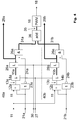
- Fig. 1 shows the block diagram of the overall digital circuit according to the invention in accordance with the known measuring principle, with the detection of an object moving into the transmission path I 1 recognizing an approximation thereof and thus the (transmission) property of the transmission path I 1 , here the size of the signal of a useful signal transmitter 2, is examined on the basis of the measurement signal of a receiver 3. After receiving the signal of the useful signal transmitter 2 by a receiver 3, for example by a photodiode, its analog output signal 4 is first digitized. In order to meet the demands of a fully digital design, the use of a conventional ADC should be avoided. The ADC should therefore, as far as possible, be independent of parameter fluctuations in a semiconductor process.
- a High-pass filter (here, for example, specifically in the form of a discrete capacitor 5) connected in series with the output signal 4 of the receiver 3. This is charged to a voltage such that it approximately compensates for the voltage difference between the voltage operating point of the receiver 3, for example a photodiode, and the switching threshold of a subsequent inverter 22. In the idle state, the input of the inverter 22 is therefore exactly at the switchover point thereof.
- the output 8 of the inverter 22 is fed back to the input via a discrete, typically chip-external, low-pass filter 10 comprising, for example, two resistors 10a, 10b and a capacitor 10c. Its resistors 10a, 10b form a voltage divider with a further resistor 7 connected to ground at the feedback node or input of the inverter 22, via which the operating point is set.
- a discrete, typically chip-external, low-pass filter 10 comprising, for example, two resistors 10a, 10b and a capacitor 10c.
- Its resistors 10a, 10b form a voltage divider with a further resistor 7 connected to ground at the feedback node or input of the inverter 22, via which the operating point is set.
- This in Fig. 1 D-flip-flop 9 shown (synchronization flip-flop) will be explained later in its function and serves to improve performance. It has been shown that this flip-flop 9 is advantageous. For the immediate understanding of the invention and its basic function, however
- the input 6 of the inverter 22 does not reach the switching threshold thereof and the output 8 is high. This leads to a current through the resistors 10a and 10b and thus to the charging of the capacitor 5. If the switching threshold of the inverter 22 is reached at the inverter input 6, the charging process ends and a discharging process begins. If the voltage at the inverter input 6 is too high, the inverter output 8 is low and there is a discharge current through the resistor 7 and the resistors 10b and 10a.
- the capacitor 10c of the filter 10 is used for low-pass filtering of the feedback signal.
- the inserted D-flip-flop 9, clocked with the system clock 27, serves the same purpose, which samples the signal at the inverter output 8 and performs the same function as a sample-and-hold circuit that would be at the input 6 of the inverter would be located and would synchronize the analog output signal of the receiver with an analog level in the system clock.
- a double discretization is carried out by this stage, on the one hand, the receiver output signal 4 is sampled. On the other hand, it is mapped to a discrete digital voltage level.
- the synchronous one-bit output signal 11 of the one-bit analog-digital converter generated in this way is digitally multiplied by the transmission signal 21 to form the signal 13. This is done by an EXOR gate 12.
- a low level of the one-bit output signal 11 corresponds to a -1 and a high level corresponds to a 1.
- a high level of the transmission signal 21 corresponds to a 1 and a low level one -1.
- This transmission signal 21 is generated in addition to other control signals by a central automaton (generator 25) from the system clock (clock 27).
- the transmission signal is sent by the useful signal transmitter 2 to said receiver 3 via a first, unknown transmission channel.
- the useful signal transmitter 2 can be, for example, an LED (light-emitting diode) or another electromagnetic transmitter.
- the receiver 3 can be a corresponding receiver.
- this would be a photodiode, for example.
- the multiplied receiver output signal 13 formed by the multiplication described above is summed up by an up-down counter 14.
- not all bits of the output signal 15 of the up-down counter 14 are passed to the subsequent PWM unit 16, but only the higher-order bits. This creates an integrating filter effect.
- the PWM unit 16 sends in PWM periods 32 (in Fig. 2 the periods 32a, 32b, 32c and 32d).
- multiple PWM periods result in 32 (in Fig. 2 the periods 32a, 32b, 32c and 32d) the basic period of the transmission signal 21.
- the PWM signal 17 obtained in this way is multiplied in an AND gate 26 by the transmission signal 21 inverted in the inverter 23 (the inverted transmission signal 24).
- the low level of the inverted transmission signal 24 corresponds to 0 and the high level to 1.
- an AND gate can be used in this multiplication instead of the EXOR gate used in the first multiplication.
- the output 18 of the AND gate 26 typically feeds the compensation signal transmitter 1 via a driver or series resistor 19.
- the signal 29 and the inverted transmission signal 24 can be present at the input of the AND gate 26, the output signal of the AND gate 26 being fed to a PWM unit 16, the output 18 of which feeds the compensation signal transmitter 1 (possibly via a driver or series resistor) .
- the useful signal transmitter 2 typically transmits its signal via a transmission link I 1 with unknown properties that need to be determined, while the transmission of the compensation signal transmitter 1 reaches the receiver via a substantially known transmission link I 2 .
- the transmission pauses of the useful signal transmitter 2 are compensated by the compensation signal transmitter 1, so that the signal at the input 6 is more or less a DC signal.
- the inverter 22 therefore always fluctuates a little around its switching threshold, which leads to oscillations which are further excited by the system noise.
- the flip-flop 9 has proven to be very helpful, since it synchronizes the oscillations with the system clock and suppresses all non-synchronous vibrations. The fluctuations that still occur are further reduced by reducing the bus width of signal 29 compared to output signal 15.
- the up-down counter 14 thus has the function of a low-pass filter.
- the stage consisting of EXOR gate 12, up-down counter 14 and register 28 carries out scalar multiplication of the digital signal 21 with the output signal 11 of the analog-digital converter.
- the value of the signal 29 therefore indicates how much of the transmission signal 21 is contained in the synchronized output signal 11.
- the central control unit 25 is typically connected to the up-down counter 14 and the PWM unit 16 in such a way that they run synchronously with one another. This synchronization is ensured by a synchronization signal, which in Fig. 1 are not shown.
- the transmission signal 21 which is generated by the central control unit 25, synchronized with the PWM exchange of words.
- this alternating frequency of the transmission signal 21 has been selected four times as low as the PWM word frequency.
- the PWM word frequency is the inverse of the PWM period 32.
- the AC frequency is the inverse of the transmit signal period 33.
- the PWM unit 16 is modulated so that it transmits with the highest possible frequency.
- VHDL High Speed Integrated Circuit Hardware Description Language
- the PWM periods 32 do not comprise 2 n but only 2 n -1 bits, ie 2 n -1 clocks of the system clock 27.
- the signal is symmetrical around the temporal center of gravity, ie half the PWM period 32, which is a significant advantage since the PWM jitter is thereby limited to half a clock width.
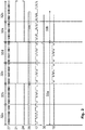
- Fig. 2 shows a corresponding timing diagram for a 3 bit PWM unit.
- a 3-bit PWM unit was chosen solely because of the clearer presentation, although based on experience an 8-bit PWM unit is better.
- System clock 27 synchronizes all logic. For the example of a 3-bit PWM unit, a PWM period takes seven system clocks 27.
- each transmission period 33 consists of four PWM periods 32a, 32b, 32c, 32d. This relationship has proven to be useful in an application of the invention. Other conditions are possible.
- the transmission signal 21 changes the logic value synchronously with the start of a new PWM period 33b.
- the same also applies to the inverted transmission signal 24.
- the value of the up-down counter is stored with a control signal 30 in the last cycle of the previous transmission signal period 33a and is for the logical content of the PWM output signal 17 in the subsequent transmission signal Period 33b is decisive.
- the compensation transmission signal is obtained at the output 18 of the AND gate 26 by multiplying the PWM output signal 17 by the inverted transmission signal 24.
- the first multiplication of the synchronized inverter output signal 11 with the transmit signal 21 in the EXOR gate 12 and the subsequent integration by the up-down counter 14 can be understood as forming a scalar product of two functions.
- the period T corresponds to the period of the transmission signal 21, for example.
- the scalar product formation is only completed with the last cycle. In the example, this is done by storing the counter reading of the up-down counter 14 in the register 28 at the end of a transmission period 33. This is initiated by the control signal 30. The value corresponds to a Fourier coefficient for the transmission signal 21.
- the PWM unit 16 may make sense to reverse the order of the PWM unit 16 and the second multiplication by the AND gate 26.
- the PWM unit can then be used for several scalar products by summation at the same time. This difference is in the Fig. 7 and 8th shown.
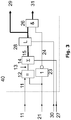
- Fig. 3 shows such a unit 40.
- each parallel bit of the signal 29 with the inverted transmit signal 24 is individually multiplied by a separate AND gate 26.
- the result is the back-transformed data bus 31.
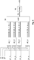
- Fig. 4 shows how two such units 40, here designated 40a and 40b, are used.
- the first unit 40a executes the dot product between the synchronized inverter output signal 11 and a first transmission signal 21a.
- the second unit 40b carries out the dot product between the synchronized inverter output signal 11 and a second transmission signal 21b.
- Regarding the conditions for the signals 21a and 21b here again EP-A-2 631 674 referred. It is particularly expedient if the signals 21a and 21b are orthogonal to one another with respect to the realized scalar products.
- the subunits are also labeled a and b for better differentiation.
- the two compensation data streams 31a and 31b are combined in an adder 36 to form the back-transformed data stream 35. This feeds the PWM unit 16, which now generates a common compensation transmission signal directly as the output signal 18.
- the Fourier coefficients for the signals 21a and 21b are then in the form of two digital values 29a and 29b.
- the PWM unit 16 forms a DAC with a downstream decimation filter (for example realized by an RC low-pass filter from, for example, the resistor 19 and the parasitic capacitance of the compensation signal transmitter 1) ( Fig. 5 and 6 ).
- a downstream decimation filter for example realized by an RC low-pass filter from, for example, the resistor 19 and the parasitic capacitance of the compensation signal transmitter 1.
- Fig. 5 and 6 The use of a PWM unit as a DAC is not absolutely necessary. Other converter principles can also be used with appropriate adaptation.
- Fig. 6 therefore shows a construction with an analog output 37 and any DAC.
- the DAC or the PWM unit 16 can be integrated with the unit 40 to form a new block 39 ( Fig. 8 ).
- Fig. 9 is shown that the multiplication AND gate 26 compared to Fig. 9 can be moved behind the PWM unit 16.
- decimation filter 41 instead of the decimation filter 10, other decimation filters 41 can also be used. This is in Fig. 11 shown.
- a common PWM unit 16 must be provided for DA conversion.
- the units 40_g and 40_s which correspond inside a unit 40, provide two digital values 31_g and 31_s, which in the adder 36 add to the known one back-transformed total data stream 35 can be summarized.
- the transmission signal that fluctuates between 0 and 1 (assuming an arbitrary standardization to simplify this description) and the constant 1 (again assuming arbitrary standardization to simplify this description) are not orthogonal to one another with respect to that for the Constant dot product to be formed.
- a scalar product of the transmission signal which is assumed to fluctuate between 1 and 0 with a 50% duty cycle, results in a constant value of 0.5 and not 1. Therefore, for correct orthogonalization, half the value 31_s of the Transmission signal 21 associated scalar product from unit 40_s are subtracted from the result 31_g of the scalar product 31_g assigned to the constant. This is done by copying the bits of the data signal bus 31_s into a data bus 42 which is one bit narrower before the addition. This is in Fig. 13 shown.
- the load resistance R 42 42 of the receiving diode of the receiver 3 and the (discharge) resistor 7 (R 7 ) are denoted by R 42 and R 7 in the following formulas, the capacitor 5 by C 4 .
- the signal motion picture can be in Fig. 15 deduce.
- the analog feedback signal 43 multiplied by a factor k 1 is added to the input signal i 3 at the point "in".
- the time integral of this signal 43 multiplied by a factor k 2 is also added.
- a multiplication by a constant k 3 takes place . If a limit value is exceeded, this signal is mapped to a 1 and otherwise to a 0 by an ideal one-bit ADC 44.
- the signal a (t) results.
- the scalar product formation preferably follows by multiplication with the signal b (t) and subsequent integration over the period of the signal b (t) or the period of the system, for example over the period of the signal 21 (not in Fig. 15 ) and multiplication by an amplification factor v 0 .
- the signal 29 is filtered 46 and multiplied to the back-transformed data bus 31.
- the DAC uses this to generate the feedback signal 43 again.
- a disadvantage of the design is that the quantization error generated by the one-bit ADC 44 is particularly high for low frequencies.
- the system is intended for a measuring section where f ⁇ 0Hz applies, the problem can be easily avoided as described above.
- the in Fig. 15 shown controller initially only correctly sets the DC operating point. This means that the capacitor C 4 5 in Fig. 14 the DC voltage difference between the switching voltage of the inverter 22 and the DC voltage component of the input signal U 42 drops.
- Fig. 16 shows the system with two signals b (t) and c (t), otherwise the system Fig. 13 or that Fig. 15 corresponds.
- a signal c (t) constant to measure the direct component of the signal a (t) via the dot product and to regulate it to zero.
- the signal b (t) should correspond to the transmission signal from the measuring transmitter.
- the signal 29 then indicates the reception strength of this signal.
- Fig. 17 shows a delta-sigma converter according to the prior art.
- the drawing is taken from the book "SR NORWORTH et. AI, Delta-Sigma-Converters Theory Design and Simulation, page 1.23" .
- Fig. 14 the input signal before the integrator is subtracted from the feedback signal.
- Fig. 14 the input signal before the integrator is subtracted from the feedback signal.
- the digitization error generated by the quantizer remains in the feedback loop. This is added up by the integrator and subtracted from the input signal, as a result of which the output signal a (t) becomes error-free on average, in particular for DC signals.
- Fig. 15 works in the intended operating mode with k 4 ⁇ 0 such that the integrator suppresses the DC component. This serves to raise the input signal to the switching threshold of the inverter, which works as a quantizer. For this reason, the delta-sigma converter according to the invention is not suitable for DC signals.
- This other construction of the Fig. 15 compared to the state of the art ( Fig. 17 ) manifests itself among other things in the other sign Fig. 17 with which the integration result in Fig. 15 is fed into the input path of the quantizer (one-bit ADC 44).
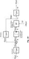
- the input signal S (j ⁇ ) is filtered with a first filter F 1 (j ⁇ ) to the signal A (j ⁇ ).
- the feedback signal G (j ⁇ ) is added to the filtered input signal A (j ⁇ ).
- the input signal B (j ⁇ ) of the one-bit analog-to-digital converter results. This is converted by the one-bit analog-to-digital converter (EADC) into a sequential one-bit data stream C (j ⁇ ).
- the output signal of the one-bit analog-to-digital converter C (j ⁇ ) corresponds to the input signal B (j ⁇ ) plus an error signal e (j ⁇ ).
- This output signal of the one-bit analog-to-digital converter C (j ⁇ ) is then sampled in a sampling circuit with a periodic sample signal clk (j ⁇ ). This corresponds to a convolution in the frequency domain.
- the intermediate value signal D (j ⁇ ) results.
- This intermediate value signal D (j ⁇ ) is then filtered by the second filter unit F 2 (j ⁇ ) to the feedback signal G (j ⁇ ) and fed to the addition already mentioned.
- the intermediate value signal D (j ⁇ ) is filtered by an output filter F 3 (j ⁇ ) to the output signal O (j ⁇ ).
- This output filter consists of a unit for scalar product formation between the transmission signal 21 and the digitized input signal 11, D (j ⁇ ). Multiplication with the transmit signal 21 follows again. Roughly speaking, it is a synchronous demodulator followed by a modulator.
- the synchronous demodulator consists of a multiplier (the EXOR gate 12) followed by an integrator (the up-down counter 14 and the latch 28).
- the PWM unit 16 is used exclusively for digital to analog conversion.
- the modulator is represented by the AND gate 26, which generates a multiplication between the signal 21 and the PWM output signal 17.
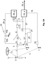
- Fig. 19 is shown which components of the circuit according to Fig. 1 the functional blocks of the Fig. 18 are to be assigned.
- SP Sample & Hold circuit
- the flip-flop 9 or the sample and hold circuit SP represents a linear form, more precisely a scalar product of the time derivative of the system clock 27 or the clock signal clk (t) and the signal am Inverter output 8 or C (t) of the one-bit analog-to-digital converter EADC or the comparator is formed.
- a further simplification can be achieved if it is assumed that the input signal A (j ⁇ ) or the output signal 4 has a signal component A a (j ⁇ ), which correlates with the clock signal clk (t) or system clock 27, and an interference signal component A b (j ⁇ ), which does not correlate with the clock signal clk (t) or system clock 27.
- G a j ⁇ F 2nd j ⁇ 1 + F 2nd j ⁇ e a j ⁇ - F 2nd j ⁇ 2nd 1 + F 2nd j ⁇ A a j ⁇
- B j ⁇ A j ⁇ + F 2nd j ⁇ 1 + F 2nd j ⁇ e a j ⁇ - F 2nd j ⁇ 2nd 1 + F 2nd j ⁇ A a j ⁇ and therefore based on equation 3:
- C. j ⁇ - A j ⁇ - F 2nd j ⁇ 1 + F 2nd j ⁇ e a j ⁇ + F 2nd j ⁇ 2nd 1 + F 2nd j ⁇ A a j ⁇ + e j ⁇
- the input signal S a (j ⁇ ) is monofrequency with a frequency ⁇ 0 .
- e a (j ⁇ ) is limited to the parts of the error that the bandpass passes.
- FIG. 20 An embodiment is shown in which instead of the one-bit ADC according to Fig. 18th and 20th a multi-bit ADC is used.
- the multi-bit analog-to-digital converter 122 converts the signal at input 6 into a digital signal 108 with a width greater than one bit.
- This digital signal 108 at the output of the multi-bit analog-to-digital converter 122 should preferably be coded with a complementary number. This means that all bits of this bus are 0 if the signal at inverter input 6 has a medium threshold. If the signal at input 6 is minimal, typically 0, all bits of signal 108 are set to 1. If the signal at input 6 is greater than or equal to the maximum value, all bits of signal 108 are also set to 1 except for the MSB. However, the MSB is still at 0.
- the bits of signal 108 are each individually connected to a flip-flop. These flip-flops together form a register 109.
- the signal 108 is sampled in this register 109.
- the scanning is typically initiated by an edge of the system clock 27. This results in the formation of said scalar product between the time derivative of the system clock 27 and the signal of the output bus 108.
- the stored signal bus 111 is passed to a digital-to-analog converter DAC 129 and is converted back by this to a feedback signal 128, which, as before, is fed back to the input of the analog-to-digital converter 122 via the low pass 10a, 10b, 10c.
- the DAC 129 supplies a medium voltage when all of its inputs, that is to say all the signals of the stored signal bus 111, are at 0.
- Each of the lines of the stored signal bus 111 is connected to an input of an EXOR gate. These EXOR gates together form an EXOR gate block 112. Each of the gates is connected to the transmit signal 21 with a second input. As a result, the transmission signal 21 again toggles the signals of the stored signal bus 111. This is almost equivalent to multiplication by -1 and 1, depending on the logical value of the transmission signal 21.
- EXOR gate block 112 multiplies the transmit signal 21 by the digitized input signal by means of the stored signal bus 111.
- the multiplied signal 113 thus obtained still corresponds to a complement number.
- This multiplied signal 113 is now added to its content by a digital integrator 114 with each cycle.
- its output that is to say the integrator output signal 115, is also a complement number.
- This integrator output signal 115 is again temporarily stored in a register 28 and implemented by a PWM unit 116.
- the difference to the previously discussed PWM unit 16 is that the PWM unit 116 still outputs a medium level as the output signal 17 when all the signals of the DAC 129 are zero, whereas in the solution described so far the old PWM in this case Unit 16 would output zero.
Landscapes
- Physics & Mathematics (AREA)
- Engineering & Computer Science (AREA)
- Electromagnetism (AREA)
- Computer Networks & Wireless Communication (AREA)
- General Physics & Mathematics (AREA)
- Radar, Positioning & Navigation (AREA)
- Remote Sensing (AREA)
- Analogue/Digital Conversion (AREA)
- Compression, Expansion, Code Conversion, And Decoders (AREA)
Claims (6)
- Dispositif de détermination d'au moins une propriété d'un canal de transmission sans fil (I1, I2) entre d'une part un émetteur de signal utile (2) destiné à émettre un signal utile binaire, ainsi qu'un émetteur de signal de compensation (1) destiné à émettre un signal de compensation binaire, et d'autre part un récepteur (3), le canal de transmission comportant un premier chemin de transmission (I1), à déterminer quant à ses propriétés, entre l'émetteur de signal utile (2) et le récepteur (3) et un deuxième chemin de transmission (I2), connu quant à ses propriétés, entre l'émetteur de signal de compensation (1) et le récepteur (3) et l'émetteur de signal utile (2) et l'émetteur de signal de compensation (1) pouvant être exploités de manière cadencée, ledit dispositif comprenant- un convertisseur analogique-numérique à un bit (22, 9, 10a, 10b, 10c) qui comporte une entrée (6) couplée à l'émetteur de signal utile (2) par le biais du récepteur (3) et une sortie (11) destinée délivrer un signal numérique,- le convertisseur analogique-numérique à un bit (22, 9, 10a, 10b, 10c) comportant un inverseur (22), qui est pourvu d'un seuil de commutation et qui comporte une entrée (6) couplée à l'entrée du convertisseur analogique-numérique à un bit (22, 9, 10a, 10b, 10c) et une sortie couplée à la sortie (11) du convertisseur analogique-numérique à un bit (22, 9, 10a, 10b, 10c), un filtre passe-bas (10a, 10b, 10c) destiné renvoyer la sortie (11) du convertisseur analogique-numérique à un bit (22, 9, 10a, 10b, 10c) à l'entrée de l'inverseur et un filtre passe-haut, se présentant en particulier sous la forme d'un condensateur (5), entre l'entrée du convertisseur analogique-numérique à un bit (22, 9, 10a, 10b, 10c) et l'entrée de l'inverseur,- une unité de produit scalaire qui comporte une unité de multiplication destinée à déterminer le produit entre le signal de sortie du convertisseur analogique-numérique à un bit (22, 9, 10a, 10b, 10c) et un signal de commande binaire (21) destiné à l'émetteur de signal utile (2) et un filtre (14) ayant un effet de filtre intégrant pour former le signal de résultat de produit scalaire (15),- l'unité de multiplication (26) comportant une porte EXOR (12) destinée à multiplier le signal de sortie à un bit à la sortie (11) du convertisseur analogique-numérique à un bit (22, 9, 10a, 10b, 10c) par le signal de commande (21) destiné à l'émetteur de signal utile (2),- une autre unité de multiplication (26) destinée à multiplier le signal de sortie (15 ou 29) du filtre (14) par un deuxième signal (24) qui est le même que le signal de commande (21) inversé logiquement destiné à l'émetteur de signal utile (2), et- une unité de génération de signal de compensation destiné à générer un signal de commande binaire destiné l'émetteur de signal de compensation (1) pour émettre le signal de compensation sur le deuxième chemin de transmission (I2) en direction du récepteur (3) dans lequel le signal de compensation et le signal utile se superposent pour former un signal d'égalité,- l'unité de génération de signal de compensation comportant un convertisseur analogique-numérique (16) destiné à convertir le signal de sortie de filtre (15 ou 29), multiplié par le deuxième signal (24), en un signal analogique servant de signal de commande destiné à l'émetteur de signal de compensation (1) et- la propriété du premier chemin de transmission (I1) pouvant être déterminée sur la base du signal de résultat de produit scalaire (15).
- Dispositif selon la revendication 1, caractérisé en ce que le convertisseur analogique-numérique comporte un circuit échantillonneur-bloqueur (9) cadencé, se présentant notamment sous la forme d'une bascule qui peut fonctionner à un multiple de la fréquence d'horloge avec laquelle le traitement de signal numérique est effectué.
- Dispositif selon la revendication 1 ou 2, caractérisé en ce que l'émetteur de signal de compensation (1) a un comportement de type passe-bas et en ce que le convertisseur numérique-analogique (16) comporte une unité PWM (16) destinée convertir le signal de résultat de produit scalaire (15 ou 29) en un signal PWM (17) et l'unité de multiplication (26) destinée à multiplier le signal de sortie (17) de l'unité PWM (16) avec le deuxième signal (24) et l'émetteur de signal de compensation (1).
- Dispositif selon l'une des revendications 1 à 3, caractérisé en ce que le convertisseur analogique-numérique à un bit (22, 9, 10a, 10b, 10c) comporte entre sa sortie (11) et son entrée (6) un chemin de rétroaction destinée à effectuer une rétraction de la sortie (11) vers l'entrée de l'inverseur et un chemin d'injection destiné au signal d'entrée (4) provenant du récepteur (3),- le signal de rétroaction (43) étant multiplié par un facteur (k1) et ajouté au signal d'entrée (4, in),- le signal de rétroaction (43) étant multiplié par un facteur (k2), intégré et ajouté au signal d'entrée,- le signal d'entrée (4, in) et ces deux signaux de sommation étant multipliés par un facteur (k4), intégrés et soustraits du signal d'entrée (4, in), le résultat de cette soustraction étant lui-même à nouveau multiplié par un facteur (k4), intégré et soustrait de lui-même, et- le résultat global formant, après multiplication par un facteur (k3), le signal d'entrée (4, in) destiné au convertisseur analogique-numérique à un bit (22, 9, 10a, 10b, 10c) du système.
- Dispositif selon l'une des revendications 1 à 4, caractérisé par un compteur décompteur (14) destiné à intégrer le produit (13) pour former le produit scalaire de l'unité de produit scalaire (12, 13, 14).
- Dispositif selon l'une des revendications 1 à 5, caractérisé en ce que l'émetteur de signal utile (2), l'émetteur de signal de compensation (1) et le récepteur (3) fonctionnent de manière optique, capacitive ou inductive.
Priority Applications (2)
| Application Number | Priority Date | Filing Date | Title |
|---|---|---|---|
| EP19217990.1A EP3657215B1 (fr) | 2012-12-21 | 2013-12-20 | Dispositif de détermination d'une propriété d'un canal de transmission entre un émetteur et un récepteur |
| EP13811245.3A EP2936201B1 (fr) | 2012-12-21 | 2013-12-20 | Dispositif de détermination d'une propriété d'un canal de transmission entre un émetteur et un récepteur |
Applications Claiming Priority (4)
| Application Number | Priority Date | Filing Date | Title |
|---|---|---|---|
| EP12199090 | 2012-12-21 | ||
| EP13186587 | 2013-09-30 | ||
| PCT/EP2013/077749 WO2014096385A1 (fr) | 2012-12-21 | 2013-12-20 | Dispositif pour déterminer une propriété d'un canal de transmission entre un émetteur et un récepteur |
| EP13811245.3A EP2936201B1 (fr) | 2012-12-21 | 2013-12-20 | Dispositif de détermination d'une propriété d'un canal de transmission entre un émetteur et un récepteur |
Related Child Applications (2)
| Application Number | Title | Priority Date | Filing Date |
|---|---|---|---|
| EP19217990.1A Division EP3657215B1 (fr) | 2012-12-21 | 2013-12-20 | Dispositif de détermination d'une propriété d'un canal de transmission entre un émetteur et un récepteur |
| EP19217990.1A Division-Into EP3657215B1 (fr) | 2012-12-21 | 2013-12-20 | Dispositif de détermination d'une propriété d'un canal de transmission entre un émetteur et un récepteur |
Publications (2)
| Publication Number | Publication Date |
|---|---|
| EP2936201A1 EP2936201A1 (fr) | 2015-10-28 |
| EP2936201B1 true EP2936201B1 (fr) | 2020-04-15 |
Family
ID=49841686
Family Applications (2)
| Application Number | Title | Priority Date | Filing Date |
|---|---|---|---|
| EP19217990.1A Active EP3657215B1 (fr) | 2012-12-21 | 2013-12-20 | Dispositif de détermination d'une propriété d'un canal de transmission entre un émetteur et un récepteur |
| EP13811245.3A Active EP2936201B1 (fr) | 2012-12-21 | 2013-12-20 | Dispositif de détermination d'une propriété d'un canal de transmission entre un émetteur et un récepteur |
Family Applications Before (1)
| Application Number | Title | Priority Date | Filing Date |
|---|---|---|---|
| EP19217990.1A Active EP3657215B1 (fr) | 2012-12-21 | 2013-12-20 | Dispositif de détermination d'une propriété d'un canal de transmission entre un émetteur et un récepteur |
Country Status (2)
| Country | Link |
|---|---|
| EP (2) | EP3657215B1 (fr) |
| WO (1) | WO2014096385A1 (fr) |
Families Citing this family (17)
| Publication number | Priority date | Publication date | Assignee | Title |
|---|---|---|---|---|
| EP3124993B1 (fr) | 2013-08-22 | 2021-10-06 | Elmos Semiconductor SE | Dispositif a compensation de defaut destine a mesurer une voie d'acheminement de signaux optiques |
| DE102015002283B4 (de) | 2014-05-09 | 2023-01-19 | Elmos Semiconductor Se | Vorrichtung zum insbesondere dreidimensionalen optischen Scannen und Vermessen von Objekten und zur Objekterkennung mittels Lichtlaufzeitmessung und objektabhängiger Ortsauflösung mehrerer verschiedener Einzelscanner |
| DE102014019773B4 (de) | 2014-12-17 | 2023-12-07 | Elmos Semiconductor Se | Vorrichtung und Verfahren zur Unterscheidung von festen Objekten, Kochdunst und Rauch mittels des Displays eines Mobiltelefons |
| DE102014019172B4 (de) | 2014-12-17 | 2023-12-07 | Elmos Semiconductor Se | Vorrichtung und Verfahren zur Unterscheidung von festen Objekten, Kochdunst und Rauch mit einem kompensierenden optischen Messsystem |
| DE102015006174B3 (de) * | 2015-05-08 | 2016-08-11 | Elmos Semiconductor Aktiengesellschaft | Vorrichtung und Verfahren zur Vermessung einer optischen, kapazitiven, induktiven Übertragungsstrecke |
| DE102017106813B4 (de) | 2016-05-09 | 2018-01-18 | Elmos Semiconductor Aktiengesellschaft | Vorrichtung und zugehöriges Verfahren zur selbständigen Adresskonfiguration konfektionierbarer, flexibler Sensor-Bänder |
| DE102017106812B4 (de) | 2016-05-09 | 2018-01-11 | Elmos Semiconductor Aktiengesellschaft | Vorrichtung und zugehöriges Verfahren zur selbständigen Adresskonfiguration konfektionierbarer, flexibler LED-Sensor-Bänder |
| DE102017106811B4 (de) | 2016-05-09 | 2018-01-11 | Elmos Semiconductor Aktiengesellschaft | Vorrichtung und zugehöriges Verfahren zur selbständigen Adresskonfiguration konfektionierbarer, flexibler LED-Bänder |
| CN106772406A (zh) * | 2016-11-29 | 2017-05-31 | 滕州市飞天激光自动化技术有限公司 | 一种可以精确控制激光探测距离的方法 |
| DE102017100308B3 (de) | 2016-12-06 | 2018-05-30 | Elmos Semiconductor Aktiengesellschaft | Vorrichtung und Verfahren zur Vermessung einer optischen, kapazitiven, induktiven Übertragungsstrecke mit verringerter EMV Empfindlichkeit |
| DE102017100306B4 (de) | 2017-01-09 | 2021-08-12 | Elmos Semiconductor Se | Vorrichtung und Verfahren zur Vermessung einer optischen, kapazitiven, induktiven Übertragungsstrecke mittels Mehrfachmodulation |
| DE102017100305B4 (de) | 2017-01-09 | 2021-08-12 | Elmos Semiconductor Se | Vorrichtung und Verfahren zur Vermessung einer optischen, kapazitiven, induktiven Übertragungsstrecke mittels Mehrfachmodulation |
| DE102019009338B4 (de) | 2019-07-23 | 2025-02-27 | Elmos Semiconductor Se | Metalllagenfreies Thermopile mit optimiertem Layout |
| DE102019119904B4 (de) | 2019-07-23 | 2024-12-19 | Elmos Semiconductor Se | Metalllagenfreies Thermopile mit optimiertem Layout |
| DE102020119245B4 (de) | 2019-07-23 | 2024-06-13 | Elmos Semiconductor Se | Halios-Vorrichtung mit metalllagenfreiem Empfänger und Kompensation mittels Phononenstrahlung eines Heizelements oder eines elektroakustischen Wandlers |
| DE102019119917B4 (de) | 2019-07-23 | 2025-02-06 | Elmos Semiconductor Se | Silizidierte Testvorrichtung und Testverfahren für metalllagenfreies Thermopaar in einer Ebene eines CMOS-Stapels |
| DE102020101997B4 (de) | 2020-01-24 | 2022-03-03 | Elmos Semiconductor Se | Gestenerkennungsvorrichtung für die Innenraumbeleuchtung von Fahrzeugen mit gleichzeitig geringem Totraum vor dem Sensorsystem |
Family Cites Families (7)
| Publication number | Priority date | Publication date | Assignee | Title |
|---|---|---|---|---|
| EP0706648B1 (fr) * | 1993-07-02 | 1997-09-03 | Gerd Reime | Systeme de mesure ou de detection d'une modification intervenant sur un element reflechissant |
| DE10300223B3 (de) | 2003-01-03 | 2004-06-24 | Gerd Reime | Optoelektronische Messanordnung mit Fremdlichtkompensation sowie Verfahren zur phasenkorrekten Kompensation eines Signals der Messanordnung |
| DE102005045993B4 (de) | 2005-07-29 | 2008-11-13 | Gerd Reime | Verfahren zur Lichtlaufzeitmessung |
| US7663521B2 (en) | 2008-03-19 | 2010-02-16 | Infineon Technologies Ag | Oversampling PID controller for integration with a delta-sigma analog-to-digital converter |
| EP2109018B1 (fr) | 2008-04-08 | 2012-05-23 | ELMOS Semiconductor AG | Circuit régulateur numérique ayant des caractéristiques de passe bas |
| DE102010028967A1 (de) | 2010-04-26 | 2011-10-27 | Balluff Gmbh | Optische Sensorvorrichtung |
| EP2631674A1 (fr) | 2012-02-23 | 2013-08-28 | ELMOS Semiconductor AG | Procédé et système de capteur destinés à la mesure des propriétés d'une voie de transmission d'un système de mesure entre émetteur et récepteur |
-
2013
- 2013-12-20 EP EP19217990.1A patent/EP3657215B1/fr active Active
- 2013-12-20 EP EP13811245.3A patent/EP2936201B1/fr active Active
- 2013-12-20 WO PCT/EP2013/077749 patent/WO2014096385A1/fr not_active Ceased
Non-Patent Citations (1)
| Title |
|---|
| None * |
Also Published As
| Publication number | Publication date |
|---|---|
| WO2014096385A1 (fr) | 2014-06-26 |
| EP2936201A1 (fr) | 2015-10-28 |
| EP3657215A1 (fr) | 2020-05-27 |
| EP3657215B1 (fr) | 2022-05-18 |
Similar Documents
| Publication | Publication Date | Title |
|---|---|---|
| EP3657215B1 (fr) | Dispositif de détermination d'une propriété d'un canal de transmission entre un émetteur et un récepteur | |
| DE10235062B4 (de) | Filterverfahren und A/D-Wandlergerät mit einer Filterfunktion | |
| DE102016119246B4 (de) | Rauscharme Präzisionseingangsstufe für Analog-Digital-Wandler | |
| DE112016002487B4 (de) | Unterdrücken von Signalübertragungsfunktionsspitzen bei einem vorwärtsgekoppelten Delta-Sigma-Wandler | |
| DE202015009602U1 (de) | LC-Gitter-Verzögerungsleitung für schnelle ADW-Anwendungen | |
| DE102015101411B4 (de) | Verbesserter Analog-Digital-Wandler und Verfahren zum Betreiben eines Analog-Digital-Wandlers | |
| DE102013109172B4 (de) | Verzögerungskompensation für Sigma-Delta-Modulator | |
| DE102008059160A1 (de) | Digital-Analog-Wandler und Integrator mit Doppelabtastung | |
| DE102018107692A1 (de) | Leistungsskalierung eines zeitkontinuierlichen Delta-Sigma-Modulators | |
| DE102016117464B4 (de) | Analog-Digital-Wandlung mit analoger Filterung | |
| DE102013002087B4 (de) | Verfahren und System zum Ausgleichen einer Verzögerungsabweichung zwischen einem ersten Messkanal und einem zweiten Messkanal | |
| DE102006023697B4 (de) | Verfahren zum Decodieren, Decodierer, Codierer-Decodierer-System und Wandler | |
| DE102004031153B4 (de) | Hochauflösender Sigma-Delta-Wandler | |
| DE10233391C1 (de) | Analog/Digital-Wandlerschaltung sowie entsprechendes Verfahren zur Analog/Digital-Wandlung und Verwendung einer selbstoszillierenden Schaltung zur Analog/Digital-Wandlung | |
| DE102006026906A1 (de) | Schaltung und Verfahren zur Pulsweitenmodulation mittels synchronisierter, selbstoszillierender Pulsweitenmodulatoren | |
| EP2850731B1 (fr) | Procédure pour supprimer une perturbation dans un processus d'échantillonnage et un dispositif de mise en oeuvre de la procédure | |
| DE102014200856B3 (de) | Delta-Sigma-Modulator | |
| EP1048112B1 (fr) | Convertisseur numerique analogique sigma-delta | |
| DE102015110450B4 (de) | Sensorsysteme mit Multi-Modus Analog-Digital-Konvertierung | |
| DE102018104530B4 (de) | Sigma-Delta-Wandler und entsprechende Verfahren | |
| EP3320618B1 (fr) | Circuit de filtrage pour filtrer un signal d'entrée d'un convertisseur analogique-numérique | |
| DE102014204518A1 (de) | Schaltungsanordnung, Analog-Digital-Wandler, Gradientenverstärker und Verfahren zur Unterdrückung von Offset, Offsetdrift und 1/f-Rauschen einer der Analog-Digital-Konvertierung | |
| DE102017101257B4 (de) | Verfahren zur optischen Vermessung der optischen Reflexionseigenschaften eines Objekts und/oder der Transmissionseigenschaften einer Übertragungsstrecke für die Verwendung in Kfz | |
| DE10156744B4 (de) | Linearer PCM/PWM-Modulator | |
| DE102023212637B3 (de) | Vorrichtung zum erzeugen eines digitalen signals abhängig von einer stromsteigung |
Legal Events
| Date | Code | Title | Description |
|---|---|---|---|
| PUAI | Public reference made under article 153(3) epc to a published international application that has entered the european phase |
Free format text: ORIGINAL CODE: 0009012 |
|
| 17P | Request for examination filed |
Effective date: 20150612 |
|
| AK | Designated contracting states |
Kind code of ref document: A1 Designated state(s): AL AT BE BG CH CY CZ DE DK EE ES FI FR GB GR HR HU IE IS IT LI LT LU LV MC MK MT NL NO PL PT RO RS SE SI SK SM TR |
|
| AX | Request for extension of the european patent |
Extension state: BA ME |
|
| RAP1 | Party data changed (applicant data changed or rights of an application transferred) |
Owner name: ELMOS SEMICONDUCTOR AKTIENGESELLSCHAFT |
|
| RAP1 | Party data changed (applicant data changed or rights of an application transferred) |
Owner name: ELMOS SEMICONDUCTOR AKTIENGESELLSCHAFT |
|
| DAX | Request for extension of the european patent (deleted) | ||
| STAA | Information on the status of an ep patent application or granted ep patent |
Free format text: STATUS: EXAMINATION IS IN PROGRESS |
|
| 17Q | First examination report despatched |
Effective date: 20190502 |
|
| GRAP | Despatch of communication of intention to grant a patent |
Free format text: ORIGINAL CODE: EPIDOSNIGR1 |
|
| STAA | Information on the status of an ep patent application or granted ep patent |
Free format text: STATUS: GRANT OF PATENT IS INTENDED |
|
| INTG | Intention to grant announced |
Effective date: 20191122 |
|
| GRAS | Grant fee paid |
Free format text: ORIGINAL CODE: EPIDOSNIGR3 |
|
| GRAA | (expected) grant |
Free format text: ORIGINAL CODE: 0009210 |
|
| STAA | Information on the status of an ep patent application or granted ep patent |
Free format text: STATUS: THE PATENT HAS BEEN GRANTED |
|
| AK | Designated contracting states |
Kind code of ref document: B1 Designated state(s): AL AT BE BG CH CY CZ DE DK EE ES FI FR GB GR HR HU IE IS IT LI LT LU LV MC MK MT NL NO PL PT RO RS SE SI SK SM TR |
|
| REG | Reference to a national code |
Ref country code: CH Ref legal event code: EP |
|
| REG | Reference to a national code |
Ref country code: DE Ref legal event code: R096 Ref document number: 502013014596 Country of ref document: DE |
|
| REG | Reference to a national code |
Ref country code: IE Ref legal event code: FG4D Free format text: LANGUAGE OF EP DOCUMENT: GERMAN |
|
| REG | Reference to a national code |
Ref country code: AT Ref legal event code: REF Ref document number: 1257972 Country of ref document: AT Kind code of ref document: T Effective date: 20200515 |
|
| REG | Reference to a national code |
Ref country code: DE Ref legal event code: R082 Ref document number: 502013014596 Country of ref document: DE Representative=s name: DOMPATENT VON KREISLER SELTING WERNER - PARTNE, DE Ref country code: DE Ref legal event code: R081 Ref document number: 502013014596 Country of ref document: DE Owner name: ELMOS SEMICONDUCTOR SE, DE Free format text: FORMER OWNER: ELMOS SEMICONDUCTOR AKTIENGESELLSCHAFT, 44227 DORTMUND, DE |
|
| REG | Reference to a national code |
Ref country code: NL Ref legal event code: MP Effective date: 20200415 |
|
| REG | Reference to a national code |
Ref country code: LT Ref legal event code: MG4D |
|
| RAP2 | Party data changed (patent owner data changed or rights of a patent transferred) |
Owner name: ELMOS SEMICONDUCTOR SE |
|
| PG25 | Lapsed in a contracting state [announced via postgrant information from national office to epo] |
Ref country code: NL Free format text: LAPSE BECAUSE OF FAILURE TO SUBMIT A TRANSLATION OF THE DESCRIPTION OR TO PAY THE FEE WITHIN THE PRESCRIBED TIME-LIMIT Effective date: 20200415 Ref country code: IS Free format text: LAPSE BECAUSE OF FAILURE TO SUBMIT A TRANSLATION OF THE DESCRIPTION OR TO PAY THE FEE WITHIN THE PRESCRIBED TIME-LIMIT Effective date: 20200815 Ref country code: SE Free format text: LAPSE BECAUSE OF FAILURE TO SUBMIT A TRANSLATION OF THE DESCRIPTION OR TO PAY THE FEE WITHIN THE PRESCRIBED TIME-LIMIT Effective date: 20200415 Ref country code: PT Free format text: LAPSE BECAUSE OF FAILURE TO SUBMIT A TRANSLATION OF THE DESCRIPTION OR TO PAY THE FEE WITHIN THE PRESCRIBED TIME-LIMIT Effective date: 20200817 Ref country code: LT Free format text: LAPSE BECAUSE OF FAILURE TO SUBMIT A TRANSLATION OF THE DESCRIPTION OR TO PAY THE FEE WITHIN THE PRESCRIBED TIME-LIMIT Effective date: 20200415 Ref country code: GR Free format text: LAPSE BECAUSE OF FAILURE TO SUBMIT A TRANSLATION OF THE DESCRIPTION OR TO PAY THE FEE WITHIN THE PRESCRIBED TIME-LIMIT Effective date: 20200716 Ref country code: FI Free format text: LAPSE BECAUSE OF FAILURE TO SUBMIT A TRANSLATION OF THE DESCRIPTION OR TO PAY THE FEE WITHIN THE PRESCRIBED TIME-LIMIT Effective date: 20200415 Ref country code: NO Free format text: LAPSE BECAUSE OF FAILURE TO SUBMIT A TRANSLATION OF THE DESCRIPTION OR TO PAY THE FEE WITHIN THE PRESCRIBED TIME-LIMIT Effective date: 20200715 |
|
| PG25 | Lapsed in a contracting state [announced via postgrant information from national office to epo] |
Ref country code: HR Free format text: LAPSE BECAUSE OF FAILURE TO SUBMIT A TRANSLATION OF THE DESCRIPTION OR TO PAY THE FEE WITHIN THE PRESCRIBED TIME-LIMIT Effective date: 20200415 Ref country code: LV Free format text: LAPSE BECAUSE OF FAILURE TO SUBMIT A TRANSLATION OF THE DESCRIPTION OR TO PAY THE FEE WITHIN THE PRESCRIBED TIME-LIMIT Effective date: 20200415 Ref country code: BG Free format text: LAPSE BECAUSE OF FAILURE TO SUBMIT A TRANSLATION OF THE DESCRIPTION OR TO PAY THE FEE WITHIN THE PRESCRIBED TIME-LIMIT Effective date: 20200715 Ref country code: RS Free format text: LAPSE BECAUSE OF FAILURE TO SUBMIT A TRANSLATION OF THE DESCRIPTION OR TO PAY THE FEE WITHIN THE PRESCRIBED TIME-LIMIT Effective date: 20200415 |
|
| PG25 | Lapsed in a contracting state [announced via postgrant information from national office to epo] |
Ref country code: AL Free format text: LAPSE BECAUSE OF FAILURE TO SUBMIT A TRANSLATION OF THE DESCRIPTION OR TO PAY THE FEE WITHIN THE PRESCRIBED TIME-LIMIT Effective date: 20200415 |
|
| REG | Reference to a national code |
Ref country code: DE Ref legal event code: R097 Ref document number: 502013014596 Country of ref document: DE |
|
| PG25 | Lapsed in a contracting state [announced via postgrant information from national office to epo] |
Ref country code: EE Free format text: LAPSE BECAUSE OF FAILURE TO SUBMIT A TRANSLATION OF THE DESCRIPTION OR TO PAY THE FEE WITHIN THE PRESCRIBED TIME-LIMIT Effective date: 20200415 Ref country code: SM Free format text: LAPSE BECAUSE OF FAILURE TO SUBMIT A TRANSLATION OF THE DESCRIPTION OR TO PAY THE FEE WITHIN THE PRESCRIBED TIME-LIMIT Effective date: 20200415 Ref country code: DK Free format text: LAPSE BECAUSE OF FAILURE TO SUBMIT A TRANSLATION OF THE DESCRIPTION OR TO PAY THE FEE WITHIN THE PRESCRIBED TIME-LIMIT Effective date: 20200415 Ref country code: RO Free format text: LAPSE BECAUSE OF FAILURE TO SUBMIT A TRANSLATION OF THE DESCRIPTION OR TO PAY THE FEE WITHIN THE PRESCRIBED TIME-LIMIT Effective date: 20200415 Ref country code: IT Free format text: LAPSE BECAUSE OF FAILURE TO SUBMIT A TRANSLATION OF THE DESCRIPTION OR TO PAY THE FEE WITHIN THE PRESCRIBED TIME-LIMIT Effective date: 20200415 Ref country code: CZ Free format text: LAPSE BECAUSE OF FAILURE TO SUBMIT A TRANSLATION OF THE DESCRIPTION OR TO PAY THE FEE WITHIN THE PRESCRIBED TIME-LIMIT Effective date: 20200415 Ref country code: ES Free format text: LAPSE BECAUSE OF FAILURE TO SUBMIT A TRANSLATION OF THE DESCRIPTION OR TO PAY THE FEE WITHIN THE PRESCRIBED TIME-LIMIT Effective date: 20200415 |
|
| PLBE | No opposition filed within time limit |
Free format text: ORIGINAL CODE: 0009261 |
|
| STAA | Information on the status of an ep patent application or granted ep patent |
Free format text: STATUS: NO OPPOSITION FILED WITHIN TIME LIMIT |
|
| PG25 | Lapsed in a contracting state [announced via postgrant information from national office to epo] |
Ref country code: PL Free format text: LAPSE BECAUSE OF FAILURE TO SUBMIT A TRANSLATION OF THE DESCRIPTION OR TO PAY THE FEE WITHIN THE PRESCRIBED TIME-LIMIT Effective date: 20200415 Ref country code: SK Free format text: LAPSE BECAUSE OF FAILURE TO SUBMIT A TRANSLATION OF THE DESCRIPTION OR TO PAY THE FEE WITHIN THE PRESCRIBED TIME-LIMIT Effective date: 20200415 |
|
| 26N | No opposition filed |
Effective date: 20210118 |
|
| PG25 | Lapsed in a contracting state [announced via postgrant information from national office to epo] |
Ref country code: SI Free format text: LAPSE BECAUSE OF FAILURE TO SUBMIT A TRANSLATION OF THE DESCRIPTION OR TO PAY THE FEE WITHIN THE PRESCRIBED TIME-LIMIT Effective date: 20200415 |
|
| REG | Reference to a national code |
Ref country code: CH Ref legal event code: PL |
|
| GBPC | Gb: european patent ceased through non-payment of renewal fee |
Effective date: 20201220 |
|
| PG25 | Lapsed in a contracting state [announced via postgrant information from national office to epo] |
Ref country code: MC Free format text: LAPSE BECAUSE OF FAILURE TO SUBMIT A TRANSLATION OF THE DESCRIPTION OR TO PAY THE FEE WITHIN THE PRESCRIBED TIME-LIMIT Effective date: 20200415 |
|
| REG | Reference to a national code |
Ref country code: BE Ref legal event code: MM Effective date: 20201231 |
|
| PG25 | Lapsed in a contracting state [announced via postgrant information from national office to epo] |
Ref country code: LU Free format text: LAPSE BECAUSE OF NON-PAYMENT OF DUE FEES Effective date: 20201220 Ref country code: IE Free format text: LAPSE BECAUSE OF NON-PAYMENT OF DUE FEES Effective date: 20201220 |
|
| PG25 | Lapsed in a contracting state [announced via postgrant information from national office to epo] |
Ref country code: GB Free format text: LAPSE BECAUSE OF NON-PAYMENT OF DUE FEES Effective date: 20201220 Ref country code: CH Free format text: LAPSE BECAUSE OF NON-PAYMENT OF DUE FEES Effective date: 20201231 Ref country code: LI Free format text: LAPSE BECAUSE OF NON-PAYMENT OF DUE FEES Effective date: 20201231 |
|
| REG | Reference to a national code |
Ref country code: AT Ref legal event code: MM01 Ref document number: 1257972 Country of ref document: AT Kind code of ref document: T Effective date: 20201220 |
|
| PG25 | Lapsed in a contracting state [announced via postgrant information from national office to epo] |
Ref country code: AT Free format text: LAPSE BECAUSE OF NON-PAYMENT OF DUE FEES Effective date: 20201220 |
|
| PG25 | Lapsed in a contracting state [announced via postgrant information from national office to epo] |
Ref country code: TR Free format text: LAPSE BECAUSE OF FAILURE TO SUBMIT A TRANSLATION OF THE DESCRIPTION OR TO PAY THE FEE WITHIN THE PRESCRIBED TIME-LIMIT Effective date: 20200415 Ref country code: MT Free format text: LAPSE BECAUSE OF FAILURE TO SUBMIT A TRANSLATION OF THE DESCRIPTION OR TO PAY THE FEE WITHIN THE PRESCRIBED TIME-LIMIT Effective date: 20200415 Ref country code: CY Free format text: LAPSE BECAUSE OF FAILURE TO SUBMIT A TRANSLATION OF THE DESCRIPTION OR TO PAY THE FEE WITHIN THE PRESCRIBED TIME-LIMIT Effective date: 20200415 |
|
| PG25 | Lapsed in a contracting state [announced via postgrant information from national office to epo] |
Ref country code: MK Free format text: LAPSE BECAUSE OF FAILURE TO SUBMIT A TRANSLATION OF THE DESCRIPTION OR TO PAY THE FEE WITHIN THE PRESCRIBED TIME-LIMIT Effective date: 20200415 |
|
| PG25 | Lapsed in a contracting state [announced via postgrant information from national office to epo] |
Ref country code: BE Free format text: LAPSE BECAUSE OF NON-PAYMENT OF DUE FEES Effective date: 20201231 |
|
| P01 | Opt-out of the competence of the unified patent court (upc) registered |
Effective date: 20230525 |
|
| PG25 | Lapsed in a contracting state [announced via postgrant information from national office to epo] |
Ref country code: IS Free format text: LAPSE BECAUSE OF NON-PAYMENT OF DUE FEES Effective date: 20200815 |
|
| REG | Reference to a national code |
Ref country code: DE Ref legal event code: R081 Ref document number: 502013014596 Country of ref document: DE Owner name: ELMOS SEMICONDUCTOR SE, DE Free format text: FORMER OWNER: ELMOS SEMICONDUCTOR SE, 44227 DORTMUND, DE |
|
| PGFP | Annual fee paid to national office [announced via postgrant information from national office to epo] |
Ref country code: FR Payment date: 20251217 Year of fee payment: 13 |
|
| PGFP | Annual fee paid to national office [announced via postgrant information from national office to epo] |
Ref country code: DE Payment date: 20251216 Year of fee payment: 13 |