EP2936615B1 - Multi-band antenna - Google Patents
Multi-band antenna Download PDFInfo
- Publication number
- EP2936615B1 EP2936615B1 EP13824396.9A EP13824396A EP2936615B1 EP 2936615 B1 EP2936615 B1 EP 2936615B1 EP 13824396 A EP13824396 A EP 13824396A EP 2936615 B1 EP2936615 B1 EP 2936615B1
- Authority
- EP
- European Patent Office
- Prior art keywords
- antenna
- resonant
- resonant circuits
- axis
- circuit
- Prior art date
- Legal status (The legal status is an assumption and is not a legal conclusion. Google has not performed a legal analysis and makes no representation as to the accuracy of the status listed.)
- Not-in-force
Links
- 238000010586 diagram Methods 0.000 claims description 19
- 230000005855 radiation Effects 0.000 claims description 19
- 230000008878 coupling Effects 0.000 claims description 17
- 238000010168 coupling process Methods 0.000 claims description 17
- 238000005859 coupling reaction Methods 0.000 claims description 17
- 239000004020 conductor Substances 0.000 description 7
- 238000004519 manufacturing process Methods 0.000 description 5
- 238000005259 measurement Methods 0.000 description 3
- 230000005540 biological transmission Effects 0.000 description 2
- 238000004891 communication Methods 0.000 description 2
- 238000009826 distribution Methods 0.000 description 2
- 238000012544 monitoring process Methods 0.000 description 2
- 238000004088 simulation Methods 0.000 description 2
- 238000001228 spectrum Methods 0.000 description 2
- 241001354471 Pseudobahia Species 0.000 description 1
- 238000004590 computer program Methods 0.000 description 1
- 238000010276 construction Methods 0.000 description 1
- 230000001419 dependent effect Effects 0.000 description 1
- 230000009977 dual effect Effects 0.000 description 1
- 230000000694 effects Effects 0.000 description 1
- 230000005672 electromagnetic field Effects 0.000 description 1
- 239000003292 glue Substances 0.000 description 1
- 239000011810 insulating material Substances 0.000 description 1
- 230000010354 integration Effects 0.000 description 1
Images


Classifications
-
- H—ELECTRICITY
- H01—ELECTRIC ELEMENTS
- H01Q—ANTENNAS, i.e. RADIO AERIALS
- H01Q21/00—Antenna arrays or systems
- H01Q21/06—Arrays of individually energised antenna units similarly polarised and spaced apart
- H01Q21/08—Arrays of individually energised antenna units similarly polarised and spaced apart the units being spaced along or adjacent to a rectilinear path
- H01Q21/12—Parallel arrangements of substantially straight elongated conductive units
-
- H—ELECTRICITY
- H01—ELECTRIC ELEMENTS
- H01Q—ANTENNAS, i.e. RADIO AERIALS
- H01Q9/00—Electrically-short antennas having dimensions not more than twice the operating wavelength and consisting of conductive active radiating elements
- H01Q9/04—Resonant antennas
- H01Q9/16—Resonant antennas with feed intermediate between the extremities of the antenna, e.g. centre-fed dipole
- H01Q9/26—Resonant antennas with feed intermediate between the extremities of the antenna, e.g. centre-fed dipole with folded element or elements, the folded parts being spaced apart a small fraction of operating wavelength
-
- H—ELECTRICITY
- H01—ELECTRIC ELEMENTS
- H01Q—ANTENNAS, i.e. RADIO AERIALS
- H01Q1/00—Details of, or arrangements associated with, antennas
- H01Q1/36—Structural form of radiating elements, e.g. cone, spiral, umbrella; Particular materials used therewith
- H01Q1/38—Structural form of radiating elements, e.g. cone, spiral, umbrella; Particular materials used therewith formed by a conductive layer on an insulating support
-
- H—ELECTRICITY
- H01—ELECTRIC ELEMENTS
- H01Q—ANTENNAS, i.e. RADIO AERIALS
- H01Q21/00—Antenna arrays or systems
- H01Q21/30—Combinations of separate antenna units operating in different wavebands and connected to a common feeder system
-
- H—ELECTRICITY
- H01—ELECTRIC ELEMENTS
- H01Q—ANTENNAS, i.e. RADIO AERIALS
- H01Q5/00—Arrangements for simultaneous operation of antennas on two or more different wavebands, e.g. dual-band or multi-band arrangements
- H01Q5/30—Arrangements for providing operation on different wavebands
- H01Q5/307—Individual or coupled radiating elements, each element being fed in an unspecified way
- H01Q5/342—Individual or coupled radiating elements, each element being fed in an unspecified way for different propagation modes
- H01Q5/357—Individual or coupled radiating elements, each element being fed in an unspecified way for different propagation modes using a single feed point
- H01Q5/364—Creating multiple current paths
- H01Q5/371—Branching current paths
-
- H—ELECTRICITY
- H01—ELECTRIC ELEMENTS
- H01Q—ANTENNAS, i.e. RADIO AERIALS
- H01Q5/00—Arrangements for simultaneous operation of antennas on two or more different wavebands, e.g. dual-band or multi-band arrangements
- H01Q5/40—Imbricated or interleaved structures; Combined or electromagnetically coupled arrangements, e.g. comprising two or more non-connected fed radiating elements
-
- H—ELECTRICITY
- H01—ELECTRIC ELEMENTS
- H01Q—ANTENNAS, i.e. RADIO AERIALS
- H01Q5/00—Arrangements for simultaneous operation of antennas on two or more different wavebands, e.g. dual-band or multi-band arrangements
- H01Q5/50—Feeding or matching arrangements for broad-band or multi-band operation
-
- H—ELECTRICITY
- H01—ELECTRIC ELEMENTS
- H01Q—ANTENNAS, i.e. RADIO AERIALS
- H01Q9/00—Electrically-short antennas having dimensions not more than twice the operating wavelength and consisting of conductive active radiating elements
- H01Q9/04—Resonant antennas
- H01Q9/16—Resonant antennas with feed intermediate between the extremities of the antenna, e.g. centre-fed dipole
- H01Q9/26—Resonant antennas with feed intermediate between the extremities of the antenna, e.g. centre-fed dipole with folded element or elements, the folded parts being spaced apart a small fraction of operating wavelength
- H01Q9/27—Spiral antennas
-
- H—ELECTRICITY
- H01—ELECTRIC ELEMENTS
- H01Q—ANTENNAS, i.e. RADIO AERIALS
- H01Q9/00—Electrically-short antennas having dimensions not more than twice the operating wavelength and consisting of conductive active radiating elements
- H01Q9/04—Resonant antennas
- H01Q9/16—Resonant antennas with feed intermediate between the extremities of the antenna, e.g. centre-fed dipole
- H01Q9/28—Conical, cylindrical, cage, strip, gauze, or like elements having an extended radiating surface; Elements comprising two conical surfaces having collinear axes and adjacent apices and fed by two-conductor transmission lines
- H01Q9/285—Planar dipole
-
- H—ELECTRICITY
- H01—ELECTRIC ELEMENTS
- H01Q—ANTENNAS, i.e. RADIO AERIALS
- H01Q11/00—Electrically-long antennas having dimensions more than twice the shortest operating wavelength and consisting of conductive active radiating elements
- H01Q11/02—Non-resonant antennas, e.g. travelling-wave antenna
- H01Q11/08—Helical antennas
-
- H—ELECTRICITY
- H01—ELECTRIC ELEMENTS
- H01Q—ANTENNAS, i.e. RADIO AERIALS
- H01Q3/00—Arrangements for changing or varying the orientation or the shape of the directional pattern of the waves radiated from an antenna or antenna system
- H01Q3/44—Arrangements for changing or varying the orientation or the shape of the directional pattern of the waves radiated from an antenna or antenna system varying the electric or magnetic characteristics of reflecting, refracting, or diffracting devices associated with the radiating element
-
- H—ELECTRICITY
- H01—ELECTRIC ELEMENTS
- H01Q—ANTENNAS, i.e. RADIO AERIALS
- H01Q9/00—Electrically-short antennas having dimensions not more than twice the operating wavelength and consisting of conductive active radiating elements
- H01Q9/04—Resonant antennas
- H01Q9/16—Resonant antennas with feed intermediate between the extremities of the antenna, e.g. centre-fed dipole
-
- H—ELECTRICITY
- H01—ELECTRIC ELEMENTS
- H01Q—ANTENNAS, i.e. RADIO AERIALS
- H01Q9/00—Electrically-short antennas having dimensions not more than twice the operating wavelength and consisting of conductive active radiating elements
- H01Q9/04—Resonant antennas
- H01Q9/30—Resonant antennas with feed to end of elongated active element, e.g. unipole
- H01Q9/42—Resonant antennas with feed to end of elongated active element, e.g. unipole with folded element, the folded parts being spaced apart a small fraction of the operating wavelength
Definitions
- the present invention relates to a multi-band antenna, preferably a dual-band one.
- Said antenna is preferably formed on a printed circuit board (PCB).
- PCB printed circuit board
- the antenna according to the present invention is designed for communicating within two electromagnetic spectrum portions reserved for non-commercial radio-communication applications, normally referred to as ISM (Industrial, Scientific and Medical) or SRD (Short Range Device) bands. More in detail, the antenna according to the present invention is preferably adapted to operate in bands around the 868MHz frequency, called European SRD band, the 915MHz frequency, called ISM band, and the 2.4GHz frequency, also called ISM band.
- ISM International, Scientific and Medical
- SRD Short Range Device
- the free ISM and SRD frequencies are widely used for short-range data transmission in applications such as, for example, remote monitoring and control, such as wireless sensor and actuator networks (WSN/WSAN), telemetry, alarm systems, etc.
- WSN/WSAN wireless sensor and actuator networks
- These bands are used by several low-data rate and high-data rate communication standards, such as Wi-Fi, IEEE 802.15.4, Bluetooth, ZigBee, etc.
- the devices adapted to communicate over said bands lead to applications developed through highly pervasive and device-dense systems; since said bands are widely used, they require that the cost of the device itself, and hence of the antenna which is a part thereof, is low.
- Electronic devices e.g. wireless ones, capable of operating over two or more ISM/SRD bands, are normally equipped with two or more antennae, which are substantially independent and distinct, and which are adapted to be selectively powered for the purpose of energizing the resonance modes of either antenna, depending on the frequency at which the device needs to communicate.
- PCB antennae are also known which can operate at two different frequencies, in that they include two independent antennae arranged on the same layer of insulating material or at different levels of a printed circuit.
- PCB antennae or patch antennae
- PCB antennae have a directional radiation diagram; in fact, they have the maximum radiation lobe in a direction substantially perpendicular to the surface of the printed circuit board on which the antenna is provided.
- Patent applications are also known which describe nonlinear antennae wound around themselves, in particular consisting of straight sections so structured as to create a spiral-wound broken line, thus minimizing space occupation.
- Another known problem concerns the cross-talk between two near antennae, which, although they operate at different frequencies, interact electromagnetically with each other.
- an antenna device has at least one linear conductor each having one or more bent or curved portions for a feeder section.
- the present invention aims at solving the above-mentioned technical problems by providing a PCB antenna which can operate over more than one band without requiring the intervention of any multiplexing devices for selecting the most suitable antenna for the band of interest.
- One aspect of the present invention relates to an antenna having the features set out in the appended independent claim 1.
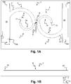
- multi-band antenna 3, associable with an electronic device comprises a single power supply point 31.
- antenna 3 is designed as a balanced one. If it has to be associated with a floating-mass or single-ended transceiver, the power supply point will in turn be connected to the output terminal of a balun adapter circuit "B".
- antenna 3 comprises at least one first resonant circuit 5, preferably adapted to resonate at a first frequency "f1”, e.g. in the 868MHz SRD band, and at least one second resonant circuit 7, preferably adapted to resonate at a second frequency "f2", e.g. in the 2.4GHz ISM band.
- the term "resonant circuit” refers to a portion of conductive material adapted to radiate and/or receive an electromagnetic field in a predetermined band of the frequency spectrum.
- Resonant circuits (5, 7) are electrically connected to each other, and the connection point between the resonant circuits corresponds to the power supply point 31, as shown, for example, in Figure 1A and Figure 2 .
- Resonant circuits (5, 7) are energized through said power supply point 31 by forcing a radio-frequency signal in the operating frequency band of each resonant circuit.
- Each resonant circuit (5, 7) substantially forms a virtual antenna.
- Such a configuration allows antenna 3 to be used simultaneously over multiple bands.
- Said resonant circuits (5, 7) are arranged in the same reference plane "XY” defined by a first axis "X” and a second axis "Y”, which are perpendicular to each other.
- said resonant circuits (5, 7) are arranged in parallel planes, along a third axis "Z" which is perpendicular to both the first axis "X” and the second axis "Y", wherein the projections of both of said first axis "X” and said second axis "Y”, with respect to planes perpendicular to both parallel planes, lie in both parallel planes.
- Each resonant circuit (5, 7) comprises at least one curvilinear portion (54, 74).
- Said curvilinear portions (54, 74) of resonant circuits (5, 7), lying in the same plane or in parallel planes, are arranged symmetrically; two curvilinear portions comprised in two resonant circuits are arranged symmetrically, preferably specularly, with respect to the first axis "X", e.g. as shown in the drawings.
- the arrangement of the curvilinear portions of the resonant circuits is such as to minimize the coupling between the same resonant circuits (5, 7).
- the radiation diagram of antenna 3 according to the present invention at the operating frequencies (f1, f2) is a function of the radius of curvature of curvilinear portions (54, 74) of the respective resonant circuits (5,7).
- curvilinear portions (54, 74) will have different radii of curvature as well as different longitudinal extensions, as is clearly visible in Figures 1A and 2 .
- Curvilinear portions (54, 74) of resonant circuits (5, 7) are symmetrical to each other with respect to said first axis "X", thus reducing to a minimum the coupling between resonant circuits (5, 7) and allowing the antenna to be used simultaneously over multiple bands, while minimizing mutual interference.
- curvilinear portions arranged symmetrically and/or specularly with respect to the first axis "X" means that the shape of the single curvilinear portions is such that the concavities of the symmetrical curvilinear portions are different relative to the axis of symmetry, e.g. as shown in Figures 2 and 1A .
- the two curvilinear portions have opposite concavity with respect to the axis of symmetry and/or specularity "X".
- each resonant circuit is a dipole comprising two arms, respectively a first arm (51, 71) and a second arm (53, 73).
- Each one of said arms (51, 53, 71, 73) is electrically connected, at one end, to the power supply point (31).
- said antenna is a dual-band one. Said embodiment, therefore, only includes the first resonant circuit 5 and the second resonant circuit 7.
- the arms of the two resonant circuits (5, 7) are connected in pairs (51-73, 53-71) to each other, as clearly shown in Figures 1A and 2 .
- connection point between the two arms (51-73, 53-71) of the two resonant circuits (5, 7) corresponds to the power supply point 31, as shown in Figure 1A .
- the single dipoles (5, 7) are arranged in the same reference plane "XY".
- Said reference plane “XY”, as aforementioned, is defined by the first axis "X” and by the second axis "Y”, which are perpendicular to each other.
- Said reference plane “XY” corresponds, for example, to the plane defined by the printed circuit board on which the antenna according to the present invention is formed.
- each resonant circuit (5, 7) have a central symmetry configuration, e.g. they are arranged in pairs in a specular manner.
- the two arms are arranged with central symmetry, e.g. in pairs and specular with respect to the first and second axes (X, Y), which axes are perpendicular to each other and define said reference plane "XY".
- a second arm (53, 73) can be positioned with central symmetry relative to a first arm (51, 71) as follows: starting from the position of said first arm, the arm is turned over relative to the axis of symmetry "X", and it is then turned over again relative to the second axis of symmetry "Y". The intersection point between said first axis "X" and said second axis "Y" defines the centre of symmetry.
- the central symmetry arrangement, e.g. in pairs and specular, of the arms (53, 51, 71, 73) of each resonant circuit (5, 7) contributes to reducing the cross-talk coupling between the same resonant circuits.
- the antenna has a structure with central symmetry developed with respect to a point, called origin or point of symmetry, e.g. defined by the intersection of the two axes (X, Y). Being the centre of symmetry of the whole structure, said point or origin is by construction set to null potential or virtual mass.
- each arm (51, 53, 71, 73) of each resonant circuit comprises at least one curvilinear portion (54, 74).
- each resonant circuit (5, 7) constitutes the biggest part of each resonant circuit (5, 7); for example, each resonant circuit (5, 7) consists entirely of at least one curvilinear portion (54, 74).
- said curvilinear portion (54, 74) is the biggest part of each arm (51, 53, 71, 73). More preferably, each arm (51, 53, 71, 73) consists entirely of one curvilinear portion (54, 74).
- Each curvilinear portion (54, 74) has a known radius of curvature, preferably constant along the whole portion (54, 74).
- curvilinear portion (54, 74), associated with a resonant circuit is equal for both arms (51, 53; 71, 73) of the same resonant circuit (5, 7), so that, with respect to the other antenna, homologous circuit parts or, in particular, circuit sections are as orthogonal as possible.
- the radiation diagram of the antenna according to the present invention at the operating frequencies (f1, f2) is a function of the radius of curvature of curvilinear portions (54, 74) of arms (51, 53, 71, 73) of respective resonant circuits (5, 7).
- the arrangement of said at least one curvilinear portion (54, 74) of each resonant circuit (5, 7) is such as to minimize the coupling between resonant circuits (5, 7), thereby allowing the antenna to be simultaneously used over multiple bands, thus reducing any mutual interference between the resonant circuits.
- curvilinear portions thanks to the orthogonal homologous parts (or sections) thereof, allows to minimize any cross-talk effects between the resonant circuits.
- said curvilinear portions are adapted to make the currents flowing in the single resonant circuits orthogonal to each other, thus reducing the coupling.
- the antenna is so designed as to maximize the isotropy of the radiation diagram in all of the frequencies in which the antenna of the present invention can operate. This is achieved thanks to the shape of the antenna, which allows, for the current elements of the resonant circuits, to keep a symmetrical current distribution with respect to the power supply point, which changes direction with continuity so as to cause the radiation diagram to become more isotropic than that of a classic dipole antenna.
- the reduction of the coupling between the resonant circuits contributes to increasing the isotropy of each virtual antenna associated with the single resonant circuit.
- the behaviour of each resonant circuit is substantially identical to that of a similar resonant circuit isolated from any other resonant circuit, i.e. the resonant circuit has a real behaviour, as if there were no other resonant circuits in the vicinity, without being affected by mutual couplings which are normally present in a prior-art multi-band antenna.
- the radiation diagram is substantially isotropic.
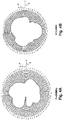
- Figures 3A and 3B show a simulation of the antenna according to the present invention, carried out by means of a computer program.
- Figures 4A and 4B show an anechoic chamber measurement of the transmission behaviour of the antenna in a section of the 3D radiation diagram shown in Figures 3A, 3B .
- the diagram of Figures 4A, 4B is obtained by turning the antenna about the second axis "Y".
- Figures 4A and 4B show the radiation diagram with respect to a second reference plane "XZ", which is defined by said first axis "X” and by a third axis "Z”.
- Said third axis "Z” is perpendicular to both said first axis "X” and said second axis "Y”.
- the minimum is located in the radiation diagram along axis "X"; such a behaviour resembles the behaviour of a dipole whose minimum or zero is found at its longitudinal axis.
- the anechoic chamber measurements thus show the proper operation of the antenna according to the present invention, demonstrating that both resonant circuits can be powered simultaneously without interacting with each other.
- the whole antenna 3 is symmetrical, with central symmetry, e.g. with a specular dual arrangement, with respect to the orthogonal axes that define reference plane "XY".
- the preferred operating frequencies of the antenna according to the present invention are the 868MHz and 2.4GHz ISM/SRD bands.
- the first resonant circuit 5 is adapted to resonate in the 868MHz SRD frequency band.
- the second resonant circuit 7 is adapted to resonate in the 2.4GHz ISM frequency band.
- the same first resonant circuit 5 is capacitively charged.
- the first resonant circuit 5 is capacitively charged by connecting, to the end of circuit 5 opposite to power supply point 31, an electric conductor 55 having a larger surface than the resonant circuit itself. Electric conductor 55 is applied to one end of each arm (51, 53) of the first resonant circuit 5.
- each curvilinear portion 54 forming an arm (51, 53), to power supply point 31 as well as to the corresponding branch of the second resonant circuit 7, whereas at its second end it is electrically connected to a second portion 55, made of conductive material.
- said second portion 55 has a longitudinal shape substantially arranged along the direction of one axis forming reference plane "XY". More in detail, each second portion 55 is substantially aligned with or parallel to the second axis "Y", as shown in Figure 1A and Figure 2 .
- each one of said second portions 55 there is, at the longitudinal ends of said second portions, a fastening area 55b with no conductive material.
- said fastening areas 55b holes can be drilled in said printed circuit board without jeopardizing the antenna's functionality, for the purpose of fastening the antenna through suitable fastening means, such as screws or bolts or glue or anchors, to the structure of the device in which it will have to operate.
- Said areas turn out to be aligned with the fastening areas of most off-the-shelf enclosures having the same size as the antenna.
- the geometry used for designing the curvilinear portions (54, 74) of conductive material is such as to create a semicircumference, with a curvature of 160° to 200°, preferably 180°.
- such a design also allows to reduce the electromagnetic coupling, such as cross-talk, between resonant circuits (5, 7), by reducing the coupling between the two single virtual antennae.
- resonant circuits (5, 7) also allows to exploit other frequency bands, for more versatility, by making appropriate configuration changes, for example by adding further resonant circuits connected to one another, etc., e.g. by means of a sunburst structure, preferably while still using the central symmetry arrangement.
- the other resonant circuits comprised in the antenna according to the present invention are also immune to the harmonic frequencies of the resonance frequency.
- the single resonant circuits are not energized by the harmonic frequencies of the resonance frequency of the single circuits.
- the currents flowing in resonant circuits (5, 7) are substantially orthogonal to each other at the centre of the antenna, where the current distributions in each resonant circuit, or arm, are greater, i.e. near the power supply point.
- Said curvilinear portion (54, 74) is therefore suitable for causing the currents of each resonant circuit (5, 7) to be orthogonal to each other, thereby reducing the coupling.
- antenna 3 is formed by two substantially semicircular, e.g. spiral-shaped, structures, arranged with central symmetry, e.g. in pairs and in a specular manner, with respect to the first and second axes (X, Y) that define the reference plane "XY".
- Power supply point 31 of the antenna is preferably located where the two semicircle-shaped or spiral-shaped structures are closest.
- the single semicircle-shaped or spiral-shaped structure consists of a combination of arms (51, 71; 53, 73) of each resonant circuit, whose curvilinear portions substantially form each a semicircle or at least a portion thereof.
- the antenna receives power via a power supply line, for example.
- One possible application of the present multi-band antenna 3 consists of wireless monitoring services.
- Antenna 3 according to the present invention can be applied to any device that needs an isotropic antenna for receiving or radiating electromagnetic signals over two or more frequency bands.
- this particular design avoids the need of using an antenna demultiplexer, and both antennae can be powered simultaneously from the same power supply point, where the output of the balun adapter circuit "B" can be connected, if required.
- the isotropy of the radiation diagram of the antenna is very high, as shown in Figures 3A, 3B , 4A and 4B , so that the latter can be more easily installed in different positions and environments, thus reducing the inevitable position constraints which are typical of PCB or microstrip antennae.
- the solution proposed by the present invention provides significant savings as concerns the antenna's design and manufacturing costs; in fact, in spite of its small dimensions, the antenna still ensures a substantially isotropic radiation diagram and reduced cross-talk interference between the resonant circuits.
- the small dimensions allow antenna 3 to be used in applications where space saving is a priority.
- said Balun is preferably a broadband one, so that it can be used in all of the frequency bands in which the multi-band antenna 3 operates.
- SAXON The antenna, called “SAXON” by the Applicant, is an easy-to-use, general purpose unit that costs less than any other solution currently available on the market.
- the antenna according to the present invention allows to minimize the coupling, e.g. cross-talk, between the resonant circuits, so that it can be simultaneously used over multiple bands without mutual interference.
- REFERENCE NUMERALS Antenna 3 Power supply point 31 First resonant circuit 5 First arm 51 Second arm 53 Curvilinear portion 54 Linear portion 55 Fastening area 55b Second resonant circuit 7 First arm 71 Second arm 73 Curvilinear portion 74 Balun adapter circuit B First frequency f1 Second frequency f2 Reference plane XY Second reference plane XZ First axis X Second axis Y Third axis Z
Landscapes
- Physics & Mathematics (AREA)
- Electromagnetism (AREA)
- Waveguide Aerials (AREA)
- Variable-Direction Aerials And Aerial Arrays (AREA)
- Details Of Aerials (AREA)
Applications Claiming Priority (2)
| Application Number | Priority Date | Filing Date | Title |
|---|---|---|---|
| IT001097A ITTO20121097A1 (it) | 2012-12-18 | 2012-12-18 | Antenna multibanda |
| PCT/IB2013/060989 WO2014097118A1 (en) | 2012-12-18 | 2013-12-16 | Multi-band antenna |
Publications (2)
| Publication Number | Publication Date |
|---|---|
| EP2936615A1 EP2936615A1 (en) | 2015-10-28 |
| EP2936615B1 true EP2936615B1 (en) | 2018-08-22 |
Family
ID=47683958
Family Applications (1)
| Application Number | Title | Priority Date | Filing Date |
|---|---|---|---|
| EP13824396.9A Not-in-force EP2936615B1 (en) | 2012-12-18 | 2013-12-16 | Multi-band antenna |
Country Status (4)
| Country | Link |
|---|---|
| US (1) | US9614287B2 (it) |
| EP (1) | EP2936615B1 (it) |
| IT (1) | ITTO20121097A1 (it) |
| WO (1) | WO2014097118A1 (it) |
Cited By (1)
| Publication number | Priority date | Publication date | Assignee | Title |
|---|---|---|---|---|
| US20240162619A1 (en) * | 2022-11-11 | 2024-05-16 | Tokyo Electron Limited | Parallel Resonance Antenna for Radial Plasma Control |
Families Citing this family (5)
| Publication number | Priority date | Publication date | Assignee | Title |
|---|---|---|---|---|
| US10476293B2 (en) * | 2016-04-06 | 2019-11-12 | Analog Devices, Inc. | Flexible energy harvesting antenna |
| NL2018147B1 (en) * | 2017-01-09 | 2018-07-25 | The Antenna Company International N V | GNSS antenna, GNSS module, and vehicle having such a GNSS module |
| CN108767453A (zh) * | 2018-04-26 | 2018-11-06 | 西安电子科技大学 | 一种柔性超宽带mimo天线 |
| TWI731792B (zh) * | 2020-09-23 | 2021-06-21 | 智易科技股份有限公司 | 具有雙頻天線的傳輸結構 |
| CN222380847U (zh) * | 2024-05-14 | 2025-01-21 | 立讯精密工业股份有限公司 | 偶极天线 |
Family Cites Families (8)
| Publication number | Priority date | Publication date | Assignee | Title |
|---|---|---|---|---|
| EP0884796A3 (en) * | 1997-06-11 | 1999-03-24 | Matsushita Electric Industrial Co., Ltd. | Antenna device consisting of bent or curved portions of linear conductor |
| GB2347792B (en) * | 1999-03-10 | 2001-06-06 | Andrew Jesman | Antenna |
| JP2002151949A (ja) * | 2000-11-13 | 2002-05-24 | Samsung Yokohama Research Institute Co Ltd | 携帯端末機 |
| US6943734B2 (en) | 2003-03-21 | 2005-09-13 | Centurion Wireless Technologies, Inc. | Multi-band omni directional antenna |
| WO2005062422A1 (en) * | 2003-12-23 | 2005-07-07 | Macquarie University | Multi-band, broadband, fully-planar antennas |
| US20090256762A1 (en) * | 2008-04-09 | 2009-10-15 | Rcd Technology, Inc. | Rfid antenna with quarter wavelength shunt |
| US7692600B1 (en) * | 2008-10-22 | 2010-04-06 | Mobile Mark, Inc. | Internal utility meter antenna |
| TWI474560B (zh) * | 2011-01-10 | 2015-02-21 | Accton Technology Corp | 非對稱偶極天線 |
-
2012
- 2012-12-18 IT IT001097A patent/ITTO20121097A1/it unknown
-
2013
- 2013-12-16 EP EP13824396.9A patent/EP2936615B1/en not_active Not-in-force
- 2013-12-16 US US14/653,444 patent/US9614287B2/en not_active Expired - Fee Related
- 2013-12-16 WO PCT/IB2013/060989 patent/WO2014097118A1/en not_active Ceased
Non-Patent Citations (1)
| Title |
|---|
| None * |
Cited By (2)
| Publication number | Priority date | Publication date | Assignee | Title |
|---|---|---|---|---|
| US20240162619A1 (en) * | 2022-11-11 | 2024-05-16 | Tokyo Electron Limited | Parallel Resonance Antenna for Radial Plasma Control |
| US12074390B2 (en) * | 2022-11-11 | 2024-08-27 | Tokyo Electron Limited | Parallel resonance antenna for radial plasma control |
Also Published As
| Publication number | Publication date |
|---|---|
| US9614287B2 (en) | 2017-04-04 |
| WO2014097118A1 (en) | 2014-06-26 |
| US20150325920A1 (en) | 2015-11-12 |
| ITTO20121097A1 (it) | 2014-06-19 |
| EP2936615A1 (en) | 2015-10-28 |
Similar Documents
| Publication | Publication Date | Title |
|---|---|---|
| EP2936615B1 (en) | Multi-band antenna | |
| EP2752942B1 (en) | Omnidirectional antenna | |
| CN105917524B (zh) | 天线指向性控制系统以及具备天线指向性控制系统的无线装置 | |
| CN202759017U (zh) | 多频寄生耦合天线及具有耦合天线的无线通信装置 | |
| CN106415929A (zh) | 多天线以及具备该多天线的无线装置 | |
| KR101722341B1 (ko) | 모노폴과 같은 방사 특성을 가지는 이중 대역 평면형 안테나 | |
| CN102377017A (zh) | 多回圈天线系统及具有该多回圈天线系统的电子装置 | |
| CN105917523A (zh) | 便携式无线装置 | |
| US20240106129A1 (en) | Antenna, wireless communication device, and antenna forming method | |
| WO2016012738A1 (en) | Antenna and method of manufacturing an antenna | |
| US20070188399A1 (en) | Dipole antenna | |
| EP2212832B1 (en) | A radio frequency transponder and radio frequency identification system | |
| TWI462394B (zh) | 多迴圈天線系統及具有該多迴圈天線系統的電子裝置 | |
| CN104919655B (zh) | 多输入多输出天线以及无线装置 | |
| KR20140011076A (ko) | 복합 스파이럴 공진코일과 이의 제조방법, 이를 이용한 무선 전력 전송 또는수신장치 | |
| US11923622B2 (en) | Antenna and wireless communication device | |
| US8872704B2 (en) | Integrated antenna and method for operating integrated antenna device | |
| CN201937009U (zh) | 宽频倒f型天线 | |
| TWI451632B (zh) | 高增益迴圈陣列天線系統及電子裝置 | |
| US11233322B2 (en) | Communication device | |
| JP6258105B2 (ja) | アンテナ | |
| EP3503293B1 (en) | Configurable multiband wire antenna arrangement and design method thereof | |
| JP7717836B2 (ja) | 内蔵アンテナを有する照明デバイス | |
| WO2001033668A1 (en) | Dielectric antenna | |
| WO2015181510A1 (en) | Antenna |
Legal Events
| Date | Code | Title | Description |
|---|---|---|---|
| PUAI | Public reference made under article 153(3) epc to a published international application that has entered the european phase |
Free format text: ORIGINAL CODE: 0009012 |
|
| 17P | Request for examination filed |
Effective date: 20150616 |
|
| AK | Designated contracting states |
Kind code of ref document: A1 Designated state(s): AL AT BE BG CH CY CZ DE DK EE ES FI FR GB GR HR HU IE IS IT LI LT LU LV MC MK MT NL NO PL PT RO RS SE SI SK SM TR |
|
| AX | Request for extension of the european patent |
Extension state: BA ME |
|
| DAX | Request for extension of the european patent (deleted) | ||
| GRAP | Despatch of communication of intention to grant a patent |
Free format text: ORIGINAL CODE: EPIDOSNIGR1 |
|
| STAA | Information on the status of an ep patent application or granted ep patent |
Free format text: STATUS: GRANT OF PATENT IS INTENDED |
|
| INTG | Intention to grant announced |
Effective date: 20180326 |
|
| GRAS | Grant fee paid |
Free format text: ORIGINAL CODE: EPIDOSNIGR3 |
|
| GRAA | (expected) grant |
Free format text: ORIGINAL CODE: 0009210 |
|
| STAA | Information on the status of an ep patent application or granted ep patent |
Free format text: STATUS: THE PATENT HAS BEEN GRANTED |
|
| AK | Designated contracting states |
Kind code of ref document: B1 Designated state(s): AL AT BE BG CH CY CZ DE DK EE ES FI FR GB GR HR HU IE IS IT LI LT LU LV MC MK MT NL NO PL PT RO RS SE SI SK SM TR |
|
| RAP1 | Party data changed (applicant data changed or rights of an application transferred) |
Owner name: MOLTOSENSO S.R.L. |
|
| REG | Reference to a national code |
Ref country code: GB Ref legal event code: FG4D |
|
| REG | Reference to a national code |
Ref country code: CH Ref legal event code: EP |
|
| REG | Reference to a national code |
Ref country code: AT Ref legal event code: REF Ref document number: 1033537 Country of ref document: AT Kind code of ref document: T Effective date: 20180915 |
|
| REG | Reference to a national code |
Ref country code: IE Ref legal event code: FG4D |
|
| REG | Reference to a national code |
Ref country code: DE Ref legal event code: R096 Ref document number: 602013042510 Country of ref document: DE |
|
| REG | Reference to a national code |
Ref country code: NL Ref legal event code: MP Effective date: 20180822 |
|
| REG | Reference to a national code |
Ref country code: LT Ref legal event code: MG4D |
|
| PG25 | Lapsed in a contracting state [announced via postgrant information from national office to epo] |
Ref country code: NO Free format text: LAPSE BECAUSE OF FAILURE TO SUBMIT A TRANSLATION OF THE DESCRIPTION OR TO PAY THE FEE WITHIN THE PRESCRIBED TIME-LIMIT Effective date: 20181122 Ref country code: GR Free format text: LAPSE BECAUSE OF FAILURE TO SUBMIT A TRANSLATION OF THE DESCRIPTION OR TO PAY THE FEE WITHIN THE PRESCRIBED TIME-LIMIT Effective date: 20181123 Ref country code: BG Free format text: LAPSE BECAUSE OF FAILURE TO SUBMIT A TRANSLATION OF THE DESCRIPTION OR TO PAY THE FEE WITHIN THE PRESCRIBED TIME-LIMIT Effective date: 20181122 Ref country code: NL Free format text: LAPSE BECAUSE OF FAILURE TO SUBMIT A TRANSLATION OF THE DESCRIPTION OR TO PAY THE FEE WITHIN THE PRESCRIBED TIME-LIMIT Effective date: 20180822 Ref country code: SE Free format text: LAPSE BECAUSE OF FAILURE TO SUBMIT A TRANSLATION OF THE DESCRIPTION OR TO PAY THE FEE WITHIN THE PRESCRIBED TIME-LIMIT Effective date: 20180822 Ref country code: LT Free format text: LAPSE BECAUSE OF FAILURE TO SUBMIT A TRANSLATION OF THE DESCRIPTION OR TO PAY THE FEE WITHIN THE PRESCRIBED TIME-LIMIT Effective date: 20180822 Ref country code: FI Free format text: LAPSE BECAUSE OF FAILURE TO SUBMIT A TRANSLATION OF THE DESCRIPTION OR TO PAY THE FEE WITHIN THE PRESCRIBED TIME-LIMIT Effective date: 20180822 Ref country code: RS Free format text: LAPSE BECAUSE OF FAILURE TO SUBMIT A TRANSLATION OF THE DESCRIPTION OR TO PAY THE FEE WITHIN THE PRESCRIBED TIME-LIMIT Effective date: 20180822 Ref country code: IS Free format text: LAPSE BECAUSE OF FAILURE TO SUBMIT A TRANSLATION OF THE DESCRIPTION OR TO PAY THE FEE WITHIN THE PRESCRIBED TIME-LIMIT Effective date: 20181222 |
|
| REG | Reference to a national code |
Ref country code: AT Ref legal event code: MK05 Ref document number: 1033537 Country of ref document: AT Kind code of ref document: T Effective date: 20180822 |
|
| PG25 | Lapsed in a contracting state [announced via postgrant information from national office to epo] |
Ref country code: AL Free format text: LAPSE BECAUSE OF FAILURE TO SUBMIT A TRANSLATION OF THE DESCRIPTION OR TO PAY THE FEE WITHIN THE PRESCRIBED TIME-LIMIT Effective date: 20180822 Ref country code: LV Free format text: LAPSE BECAUSE OF FAILURE TO SUBMIT A TRANSLATION OF THE DESCRIPTION OR TO PAY THE FEE WITHIN THE PRESCRIBED TIME-LIMIT Effective date: 20180822 Ref country code: HR Free format text: LAPSE BECAUSE OF FAILURE TO SUBMIT A TRANSLATION OF THE DESCRIPTION OR TO PAY THE FEE WITHIN THE PRESCRIBED TIME-LIMIT Effective date: 20180822 |
|
| PG25 | Lapsed in a contracting state [announced via postgrant information from national office to epo] |
Ref country code: EE Free format text: LAPSE BECAUSE OF FAILURE TO SUBMIT A TRANSLATION OF THE DESCRIPTION OR TO PAY THE FEE WITHIN THE PRESCRIBED TIME-LIMIT Effective date: 20180822 Ref country code: PL Free format text: LAPSE BECAUSE OF FAILURE TO SUBMIT A TRANSLATION OF THE DESCRIPTION OR TO PAY THE FEE WITHIN THE PRESCRIBED TIME-LIMIT Effective date: 20180822 Ref country code: RO Free format text: LAPSE BECAUSE OF FAILURE TO SUBMIT A TRANSLATION OF THE DESCRIPTION OR TO PAY THE FEE WITHIN THE PRESCRIBED TIME-LIMIT Effective date: 20180822 Ref country code: IT Free format text: LAPSE BECAUSE OF FAILURE TO SUBMIT A TRANSLATION OF THE DESCRIPTION OR TO PAY THE FEE WITHIN THE PRESCRIBED TIME-LIMIT Effective date: 20180822 Ref country code: AT Free format text: LAPSE BECAUSE OF FAILURE TO SUBMIT A TRANSLATION OF THE DESCRIPTION OR TO PAY THE FEE WITHIN THE PRESCRIBED TIME-LIMIT Effective date: 20180822 Ref country code: CZ Free format text: LAPSE BECAUSE OF FAILURE TO SUBMIT A TRANSLATION OF THE DESCRIPTION OR TO PAY THE FEE WITHIN THE PRESCRIBED TIME-LIMIT Effective date: 20180822 Ref country code: ES Free format text: LAPSE BECAUSE OF FAILURE TO SUBMIT A TRANSLATION OF THE DESCRIPTION OR TO PAY THE FEE WITHIN THE PRESCRIBED TIME-LIMIT Effective date: 20180822 |
|
| REG | Reference to a national code |
Ref country code: DE Ref legal event code: R097 Ref document number: 602013042510 Country of ref document: DE |
|
| PG25 | Lapsed in a contracting state [announced via postgrant information from national office to epo] |
Ref country code: SK Free format text: LAPSE BECAUSE OF FAILURE TO SUBMIT A TRANSLATION OF THE DESCRIPTION OR TO PAY THE FEE WITHIN THE PRESCRIBED TIME-LIMIT Effective date: 20180822 Ref country code: DK Free format text: LAPSE BECAUSE OF FAILURE TO SUBMIT A TRANSLATION OF THE DESCRIPTION OR TO PAY THE FEE WITHIN THE PRESCRIBED TIME-LIMIT Effective date: 20180822 Ref country code: SM Free format text: LAPSE BECAUSE OF FAILURE TO SUBMIT A TRANSLATION OF THE DESCRIPTION OR TO PAY THE FEE WITHIN THE PRESCRIBED TIME-LIMIT Effective date: 20180822 |
|
| PLBE | No opposition filed within time limit |
Free format text: ORIGINAL CODE: 0009261 |
|
| STAA | Information on the status of an ep patent application or granted ep patent |
Free format text: STATUS: NO OPPOSITION FILED WITHIN TIME LIMIT |
|
| 26N | No opposition filed |
Effective date: 20190523 |
|
| REG | Reference to a national code |
Ref country code: CH Ref legal event code: PL |
|
| GBPC | Gb: european patent ceased through non-payment of renewal fee |
Effective date: 20181216 |
|
| PG25 | Lapsed in a contracting state [announced via postgrant information from national office to epo] |
Ref country code: MC Free format text: LAPSE BECAUSE OF FAILURE TO SUBMIT A TRANSLATION OF THE DESCRIPTION OR TO PAY THE FEE WITHIN THE PRESCRIBED TIME-LIMIT Effective date: 20180822 Ref country code: LU Free format text: LAPSE BECAUSE OF NON-PAYMENT OF DUE FEES Effective date: 20181216 Ref country code: SI Free format text: LAPSE BECAUSE OF FAILURE TO SUBMIT A TRANSLATION OF THE DESCRIPTION OR TO PAY THE FEE WITHIN THE PRESCRIBED TIME-LIMIT Effective date: 20180822 |
|
| REG | Reference to a national code |
Ref country code: IE Ref legal event code: MM4A |
|
| REG | Reference to a national code |
Ref country code: BE Ref legal event code: MM Effective date: 20181231 |
|
| PG25 | Lapsed in a contracting state [announced via postgrant information from national office to epo] |
Ref country code: IE Free format text: LAPSE BECAUSE OF NON-PAYMENT OF DUE FEES Effective date: 20181216 |
|
| PG25 | Lapsed in a contracting state [announced via postgrant information from national office to epo] |
Ref country code: BE Free format text: LAPSE BECAUSE OF NON-PAYMENT OF DUE FEES Effective date: 20181231 |
|
| PG25 | Lapsed in a contracting state [announced via postgrant information from national office to epo] |
Ref country code: GB Free format text: LAPSE BECAUSE OF NON-PAYMENT OF DUE FEES Effective date: 20181216 Ref country code: CH Free format text: LAPSE BECAUSE OF NON-PAYMENT OF DUE FEES Effective date: 20181231 Ref country code: LI Free format text: LAPSE BECAUSE OF NON-PAYMENT OF DUE FEES Effective date: 20181231 |
|
| PG25 | Lapsed in a contracting state [announced via postgrant information from national office to epo] |
Ref country code: MT Free format text: LAPSE BECAUSE OF NON-PAYMENT OF DUE FEES Effective date: 20181216 |
|
| PG25 | Lapsed in a contracting state [announced via postgrant information from national office to epo] |
Ref country code: TR Free format text: LAPSE BECAUSE OF FAILURE TO SUBMIT A TRANSLATION OF THE DESCRIPTION OR TO PAY THE FEE WITHIN THE PRESCRIBED TIME-LIMIT Effective date: 20180822 |
|
| PG25 | Lapsed in a contracting state [announced via postgrant information from national office to epo] |
Ref country code: PT Free format text: LAPSE BECAUSE OF FAILURE TO SUBMIT A TRANSLATION OF THE DESCRIPTION OR TO PAY THE FEE WITHIN THE PRESCRIBED TIME-LIMIT Effective date: 20180822 |
|
| PG25 | Lapsed in a contracting state [announced via postgrant information from national office to epo] |
Ref country code: CY Free format text: LAPSE BECAUSE OF FAILURE TO SUBMIT A TRANSLATION OF THE DESCRIPTION OR TO PAY THE FEE WITHIN THE PRESCRIBED TIME-LIMIT Effective date: 20180822 Ref country code: HU Free format text: LAPSE BECAUSE OF FAILURE TO SUBMIT A TRANSLATION OF THE DESCRIPTION OR TO PAY THE FEE WITHIN THE PRESCRIBED TIME-LIMIT; INVALID AB INITIO Effective date: 20131216 Ref country code: MK Free format text: LAPSE BECAUSE OF NON-PAYMENT OF DUE FEES Effective date: 20180822 |
|
| PGFP | Annual fee paid to national office [announced via postgrant information from national office to epo] |
Ref country code: DE Payment date: 20201201 Year of fee payment: 8 Ref country code: FR Payment date: 20201112 Year of fee payment: 8 |
|
| REG | Reference to a national code |
Ref country code: DE Ref legal event code: R119 Ref document number: 602013042510 Country of ref document: DE |
|
| PG25 | Lapsed in a contracting state [announced via postgrant information from national office to epo] |
Ref country code: DE Free format text: LAPSE BECAUSE OF NON-PAYMENT OF DUE FEES Effective date: 20220701 |
|
| PG25 | Lapsed in a contracting state [announced via postgrant information from national office to epo] |
Ref country code: FR Free format text: LAPSE BECAUSE OF NON-PAYMENT OF DUE FEES Effective date: 20211231 |