EP2939307B1 - Interface entre puces à plusieurs canaux, à grande vitesse et à faible puissance utilisant un guide d'ondes diélectrique - Google Patents
Interface entre puces à plusieurs canaux, à grande vitesse et à faible puissance utilisant un guide d'ondes diélectrique Download PDFInfo
- Publication number
- EP2939307B1 EP2939307B1 EP13867509.5A EP13867509A EP2939307B1 EP 2939307 B1 EP2939307 B1 EP 2939307B1 EP 13867509 A EP13867509 A EP 13867509A EP 2939307 B1 EP2939307 B1 EP 2939307B1
- Authority
- EP
- European Patent Office
- Prior art keywords
- side board
- board
- electrical
- waveguide
- fiber
- Prior art date
- Legal status (The legal status is an assumption and is not a legal conclusion. Google has not performed a legal analysis and makes no representation as to the accuracy of the status listed.)
- Active
Links
Images



Classifications
-
- H—ELECTRICITY
- H01—ELECTRIC ELEMENTS
- H01P—WAVEGUIDES; RESONATORS, LINES, OR OTHER DEVICES OF THE WAVEGUIDE TYPE
- H01P3/00—Waveguides; Transmission lines of the waveguide type
- H01P3/16—Dielectric waveguides, i.e. without a longitudinal conductor
-
- H—ELECTRICITY
- H01—ELECTRIC ELEMENTS
- H01P—WAVEGUIDES; RESONATORS, LINES, OR OTHER DEVICES OF THE WAVEGUIDE TYPE
- H01P3/00—Waveguides; Transmission lines of the waveguide type
- H01P3/12—Hollow waveguides
- H01P3/122—Dielectric loaded (not air)
-
- H—ELECTRICITY
- H01—ELECTRIC ELEMENTS
- H01P—WAVEGUIDES; RESONATORS, LINES, OR OTHER DEVICES OF THE WAVEGUIDE TYPE
- H01P5/00—Coupling devices of the waveguide type
- H01P5/08—Coupling devices of the waveguide type for linking dissimilar lines or devices
- H01P5/10—Coupling devices of the waveguide type for linking dissimilar lines or devices for coupling balanced lines or devices with unbalanced lines or devices
- H01P5/107—Hollow-waveguide/strip-line transitions
Definitions
- the present invention relates to a board-to-board interconnection device with an electrical fiber.
- US2006145778 discloses an RF interconnection between RF Printed Wiring Boards that includes a waveguide transmission line coupled between the RF Printed Wiring Boards.
- Waveguide feed circuits are use to launch signals into and couple signals out of the transmission line.
- the feed circuits are provided as micro-strip ("patch") antenna elements on Printed Wiring Board surfaces.
- the ends of the waveguide are conductively attached to the ground planes of the respective Printed Wiring Boards.
- US5528074 discloses a semiconductor device with a substrate that has a microwave semiconductor element, a microwave transmission line and a waveguide terminal structure.
- the waveguide terminal structure is connected to an end of an external waveguide. Input and output of microwave signals between the semiconductor device and an external device are carried out simply by applying an end of the external waveguide to the waveguide terminal structure.
- the external dielectric waveguide has a dielectric core, a dielectric cladding and ground metal film coating the cladding.
- US2011194240 discloses a wireless communication unit with hinged sections. An antenna is located within a first section and a radio wave transceiver section is located in a second section. A waveguide assembly provides coupling through the sections such that the antenna is electrically coupled to the radio wave transceiver section. Part of the waveguide assembly is a flexible waveguide, and the document describes the possibility of using a flexible waveguide with a dielectric core and a conductive plating, which may be copper, gold, aluminum etc.
- JP2008193161 discloses a micro strip line-waveguide converter to perform conversion between transmission modes of a micro strip line and a waveguide with a small transmission loss over a wide frequency band and having a flat frequency characteristic.
- the waveguide is formed by a hollow metal pipe with rectangular cross section.
- the micro strip line is provided on a substrate that extends perpendicularly to the axial direction of the pipe on the opening diameter of the pipe.
- the end of the strip line is located over the rectangular cross section on the top of the substrate.
- a conductor island is provides that form a patch antenna.
- the substrate of JP2008193161 comprises a stack of a plurality of dielectric layers.
- First holes penetrate the dielectric substrate layers outside an opening diameter of the waveguide.
- Second holes penetrating only the top dielectric substrate layer, are located inside the opening diameter of the waveguide. This reduces the volume of the dielectric part of JP2008193161 , making it possible to suppress the occurrence of higher-order resonance mode in the in the dielectric substrate.
- a board-to-board interconnection device according to claim 1 is provided.
- An exemplary embodiment of the present invention may provide an improved interconnect instead of electrical wire line.
- a novel type of dielectric waveguide named, for example, an electrical fiber may be presented to replace conventional copper line.
- the electrical fiber may be defined as a dielectric waveguide with metal cladding.
- Dielectrics with frequency independent attenuation characteristics may enable high data rate transfer with little or even without any additional receiver-side compensation.
- Parallel channel data transfer may be available due to vertical coupling of the electrical fiber and PCB (printed circuit board).
- the PCB with the electrical fiber for board-to-board interconnect between tranceiver I/O may be defined as a board-to-board interconnection device.
- the interconnection device may comprise the electrical fiber, a transmitter side board, a receiver side board, a board-to-fiber connector, a microstrip feeding line, a slotted ground plane, a ground plane, and a patch.
- a novel board-to-fiber connector may be presented to securely fix multiple the electrical fibers to PCB as close as to each other to maximize area efficiency.
- Physically flexible characteristic of the electrical fiber may support to connect any termination in any location in free space.
- the metal cladding of the electrical fiber may maintain the total transceiver power consumption regardless of a length of the electrical fiber.
- the cladding also may isolate the interference of the signals in other wireless channels and adjacent electrical fibers, which typically may cause band-limitation problem.
- Microstrip-to-waveguide transition may be adapted to minimize the reflection between microstrip and waveguide.
- Microstrip-to-waveguide transition may transit microstrip signal into waveguide signal, and it may have the advantage of low cost because it may be available in general PCB manufacture process
- FIG. 1 shows an isometric perspective view according to an exemplary embodiment of the invention.
- FIG.1 may illustrate the electrical fiber 101 used as a board-to-board interconnect.
- Incident signal may come from the 50-Ohm matched output of the transmitter die 102 to propagate along the transmission line 103 and then Microstrip-to-Waveguide Transition 104 (for example, MWT) on the transmitter side board may convert the microstrip signal into the waveguide signal.
- the wave for example the waveguide signal, may transmit along the electrical fiber 101 and then may be converted into microstrip signal at the MWT 105 on the receiver side board.
- signal may propagate along the transmission line 106 and then may go into the 50-Ohm matched receiver input 107.
- the dielectric waveguide may propagate a signal from the transmitter side board to the receiver side board.
- FIG. 2 shows a simplified model of the overall interconnect as a 2-Port network and a relation between reflected waves and transmitted waves at each transitions according to the exemplary embodiment of the present invention.
- impedance discontinuity may lead to inefficient transmission of energy both from the transmission line to the waveguide and from the waveguide to the transmission line.
- overall interconnect may be considered as the simple 2-port networks as FIG. 2 , Equation 1, Equation 2 and Equation 3.
- the incident waves on the transmission line side and on the waveguide side may be expressed as u 1 + and w - , respectively. And, the reflected waves may be expressed as w + and u 1 ⁇ .
- the incident waves on the waveguide side and on the transmission line side may be expressed as w +' and u 2 ⁇ .
- the reflected waves may be expressed as w -' and u 2 + .
- the following equations may express a scattering matrix (for example, S-parameter) of the overall interconnect.
- u 1 ⁇ u 2 + S 11 S 12 S 21 S 22 ⁇ u 1 + u 2 ⁇
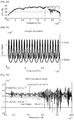
- FIG. 3 shows a graph of analytic estimation and simulated results for S-parameters of the overall interconnect constructed in accordance with the invention.
- FIG. 4 shows a graph of analytic estimation and simulated results for S-parameters of the overall interconnect constructed in accordance with the invention.
- FIG. 5 shows a graph of anlytic estimation and simulated results for Group Delay of the overall interconnect constructed in accordance with the invention.
- FIG. 3 , FIG. 4 , and FIG. 5 may show a graph of analytic estimation results for S-parameters of the overall interconnect constructed in accordance with the exemplary embodiment of the invention.
- FIG. 3 , FIG. 4 , and FIG. 5 may plot the above equation 5, equation 6, equation 7, and equation 8 and indicate the result from the different case of waveguide length (for instance, 5cm and 10cm). And each result may be compared to the simulation results from 3D Electromagnetic Simulation Tool (Ansys. HFSS).
- FIG. 3 , FIG. 4 , and FIG. 5 may say that there exists a waveguide-length- dependent-oscillation in the results of S-parameters and Group Delay of the overall interconnect.
- the oscillation in the results of S-parameters and Group Delay may result from the fact that the reflected wave occured at the impedance discontinuity undergoes a slight attenuation along the propagation and it may make a phenomenon similar to what is happening in the cavity resonator.
- the wave may bounce back and forth within the electrical fiber and reinforce the standing wave.
- the MWT may be an object of the exemplary embodiment of the present invention to provide a lower reflection (r2).
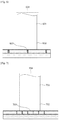
- FIG. 6 shows a side view of a waveguide to microstrip transition constructed in accordance with one embodiment of the invention.
- FIG. 7 shows a front view of a waveguide to microstrip transition constructed in accordance with one embodiment of the invention.
- FIG. 6 may show side view of the MWT and FIG. 7 may show front view of the MWT constructed in accordance with one embodiment of the invention.
- the electrical fiber 604, 704 with a metal cladding 601,701 may be in contact with the microstrip circuit, especially with a patch element 603, 703 disposed on the board.
- the metal cladding 601, 701 may wrap up a dielectric waveguide 602, 702.
- the metal cladding 601, 701 may comprise a copper cladding
- the patch element 603, 703 may comprise the microstrip line.
- the patch element 603, 703 may radiate the signal at a resonance frequency.
- the metal cladding 601, 701 may wrap up the dielectric waveguide 602, 702 with a predetermined form.
- the predetermined form of the metal cladding 601, 701 may expose a middle of the dielectric waveguide 602, 702, and the predetermined form of the metal cladding 601, 701 may be punctured to expose a specific part of the dielectric waveguide 602, 702.
- the predetermined form of the metal cladding 601, 701 may be various form.
- FIG. 8 shows an exploded view of a waveguide to microstrip transition constructed in accordance with one embodiment of the invention.
- FIG. 8 may show a detailed structure of each layer of the board.
- the 3-layers structure may be used in the manufacture of the board.
- the microstrip feeding line 801 may be located at a first floor, and the slotted ground plane 802, which is pierced by aperture, may be disposed on a second layer.
- a patch element 803 and the ground plane 804 may be disposed on a third layer.
- the microstrip feeding line 801 may feed the signal to the microstrip circuit at the first layer
- the slotted ground plane 802 may include a slot to minimize a ratio of backward propagation wave to forward propagation wave at the second layer
- the ground plane may include a via 807 to make an electrical connection between the slotted ground plane 802 and the ground plane 804 at the third layer.
- a via 807 may be disposed as an array.
- a core substrate 805 between the first and the second layer may be made of Taconic. CER-10 having dimensions of 12mm ⁇ 5.68mm and thickness of 0.28mm.
- Another core substrate 806 between the second and the third layer may be made of Rogers. RO3010 Prepreg having dimensions of 12mm ⁇ 5.68mm and thickness of 0.287mm.
- the Via 807 may play a role of making an electrical connection between the second and the third ground plane.
- the microstrip width, the substrate thickness, the slot size, the patch size, the via diameter, the via spacing, the waveguide size, the waveguide material may be modified depending on a particular resonance frequency of the microstrip circuit and the mode of the propagation wave along the electrical fiber, as it will be apparent to one skilled in the art.
- the size of the slot and the aperture may be an important factor in the transmission and reflection of the signal. Those sizes may be optimized to minimize the ratio of backward propagation wave to forward propagation wave by iterative simulation.
- a cutoff frequency and an impedance of waveguide may be determined by the dimensions of the cross section and a kind of material used. For this invention, the dimensions of 2.9mm ⁇ 2.7mm and ECCOSTOCK PP (Laird TECHNOLOGIES.) may be used to pass 60 GHz band signal with a minimum reflection at the MWT.
- FIG. 9 shows an exploded isometric view of different length of the electrical fiber with that of metal cladding and tapered waveguide constructed in accordance with one embodiment of the invention.
- This strategy may be embodied by shortening a length of the metal cladding which wraps up the dielectric waveguide of the electrical fiber 901, 902, 903 at each end.
- the metal cladding may perfectly confine the electromagnetic wave preventing a radiation loss of energy. For this reason, utilizing a short metal cladding may result in a large radiation loss. This kind of energy loss may be considered as an attenuation along the electrical fiber 901, 902, 903 and it may greatly influence the oscillation in the result of S-parameter.
- the dielectric loss may be considered as attenuation along the electrical fiber 901, 902, 903. It may result from a tangent loss of the dielectric waveguide and be relevant to the length of waveguide. The dielectric loss dissipated along the long waveguide may reduce the effect of the oscillation.
- long electrical fiber 903 may have bigger proportionality of metal cladding than short electrical fiber 901 while taking same amount of channel loss.
- One end of the electrical fiber 904 may indicate the isometric drawing of a tapered waveguide. It may be for the impedance matching between the dielectrics used for the dielectric waveguide and the microstrip circuits on the board. For example, a proportionality of a length of the metal cladding on a length of the dielectric waveguide may be designed based on a length of the electrical fiber 901, 902, 903.
- linearly shaping at least one of both ends of the dielectric waveguide may be efficient for finding optimal impedance.
- at least one of both ends of the dielectric waveguide may be tapered for impedance matching between the dielectric waveguide and microstrip circuits.
- at least one of both ends of the dielectric waveguide may be shaped linearly to optimize an impedance of the dielectric waveguide with largest power transfer efficiency.
- the interconnection device with the electrical fiber 901, 902, 903 for a board-to-board interconnect between tranceiver I/O comprising, the electrical fiber 901, 902, 903 to propagate the signal from the transmitter side board to the receiver side board with the metal cladding and the microstrip circuit to contact with the electrical fiber 901, 902, 903 with the MWT.
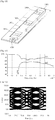
- FIG. 10 shows an isometric view of a board-to-waveguide connector constructed in accordance with an embodiment of the invention.
- FIG. 10 may show an isometric view of the board-to-fiber connector 1001.
- the electrical fiber may be firmly fixed to the board with the board-to-fiber connector 1001.
- Connector bridges 1002, 1003 may be inserted into holes bored through the board to fix it on the board.
- the board-to-fiber connector 1001 connects the electrical fiber to at least one of the transmitter side board and the receiver side board vertically.
- transition apparatuses 1004, 1005, 1006 in the connector for physical fixation of the electrical fiber.
- the electrical fiber may contact the microstrip circuit on the board. It may be a very efficient way for saving an area that the both end sides of the dielectric waveguide are vertically coupled with the transmitter side board and the receiver side board as illustrated in the FIG.10 . Because of this configuration, a number of the electrical fiber may be used to connect the multiple channels concurrently for a parallel system with wide bandwidth.
- the dielectric waveguide may be vertically coupled with at least one of the transmitter side board and the receiver side board.
- FIG. 11 shows a graph of simulated results for S-parameters of the overall interconnect constructed in accordance with one embodiment of the invention.
- simulated results for S-parameters of the overall interconnect constructed in accordance with one embodiment of the invention may be shown in the graph.
- the results may be achieved using the 50 cm electrical fiber.
- a return loss of 10 dB a 15 GHz bandwidth, from 54 GHz to 79 GHz, may be achieved.
- the insertion loss on the passband may be found to be less than 15 dB and also constant along the wide band.
- FIG. 12 shows a graph of simulated results for Eye diagram of PAM4 28Gbps PRBS 2 14 -1 for 65GHz channel.
- FIG. 12 may show an Eye-diagram of PAM4 28Gbps PRBS 2 14 -1.
- the Eye-diagram may represent the demodulated data pattern which may be modulated on the 65 GHz carrier and passed through the channel of the interconnect constructed in accordance with an exemplary embodiment.
- the electrical fiber may propose a new method to make high-speed data communication possible.
- the MWT structure may transit the wideband signal while minimizing the reflection at the discontinuity.
- the metal cladding which wraps up the dielectric waveguide may reduce the radiation loss and be effective to decrease the channel loss.
- the electrical fiber may be promising solution to I/O channel having a demand to transmit data with very high-speed.
- the electrical fiber may be able to replace the all copper wire line in the 100 Gbps backplane interface based on the IEEE 802.3 bj KR standard. And it may be applied to IEEE 802.3 bj SR standard with lengthened transmission distance.
- a board-to-board interface may take the electrical fiber as a prospective solution in the datacenter market.
Landscapes
- Waveguides (AREA)
- Combinations Of Printed Boards (AREA)
- Waveguide Connection Structure (AREA)
Claims (6)
- Dispositif d'interconnexion carte à carte au moyen d'une fibre électrique (101, 604, 704), le dispositif d'interconnexion comprenant :une carte côté émetteur et une carte côté récepteur ;une fibre électrique (101, 604, 704), configurée pour propager un signal de la carte côté émetteur à la carte côté récepteur, munie d'une gaine métallique (601, 701) ;un circuit microruban disposé sur la carte côté émetteur et la carte côté récepteur et configuré pour être en contact avec la fibre électrique (101, 604, 704) au moyen d'une transition microruban-guide d'ondes (105) ;au moins une des deux extrémités de la fibre électrique (101, 604, 704) étant effilée pour l'adaptation d'impédance entre la fibre électrique et le circuit microruban sur le dispositif d'interconnexion ;un connecteur carte à fibre (1001) configuré pour connecter de multiples fibres électriques (101, 604, 704) à au moins une de la carte côté émetteur et de la carte côté récepteur verticalement ;le connecteur carte à fibre (1001) comprenant :des ponts connecteurs (1002, 1003) insérés dans des trous percés à travers au moins une de la carte côté émetteur et de la carte côté récepteur ;de multiples appareils de transition (1004, 1005, 1006) pour la fixation physique des multiples fibres électriques, respectivement, à au moins une de la carte côté émetteur et de la carte côté récepteur.
- Dispositif d'interconnexion selon la revendication 1, dans lequel au moins une des deux extrémités de la fibre électrique est effilée linéairement pour optimiser l'impédance de la fibre électrique avec un rendement de transfert de puissance maximal.
- Dispositif d'interconnexion selon la revendication 1, dans lequel la gaine métallique comprend une gaine en cuivre.
- Dispositif d'interconnexion selon la revendication 1, dans lequel une proportion de la longueur de la gaine métallique sur la longueur de la fibre électrique est établie en fonction de la longueur de la fibre électrique.
- Dispositif d'interconnexion selon la revendication 1, le dispositif d'interconnexion comprenant en outre :une ligne d'alimentation microruban configurée pour appliquer le signal au circuit microruban au niveau d'une première couche ;un plan de masse à fente comportant une fente configurée pour réduire au minimum un rapport ondes régressives sur ondes progressives au niveau d'une deuxième couche ;un plan de masse comportant un groupement de trous d'interconnexion configurés pour établir une connexion électrique entre le plan de masse à fente et le plan de masse au niveau d'une troisième couche ; etune plaque configurée pour rayonner le signal à une fréquence de résonance.
- Dispositif d'interconnexion selon la revendication 1, dans lequel la gaine métallique enveloppe le guide d'ondes diélectrique avec une forme prédéterminée.
Applications Claiming Priority (3)
| Application Number | Priority Date | Filing Date | Title |
|---|---|---|---|
| KR1020120154094 | 2012-12-27 | ||
| KR1020130108857A KR20140086808A (ko) | 2013-09-11 | 2013-09-11 | 도파관을 이용한 멀티채널 칩대칩 저전력 고속 유선 인터페이스 |
| PCT/KR2013/008240 WO2014104536A1 (fr) | 2012-12-27 | 2013-09-12 | Interface entre puces à plusieurs canaux, à grande vitesse et à faible puissance utilisant un guide d'ondes diélectrique |
Publications (3)
| Publication Number | Publication Date |
|---|---|
| EP2939307A1 EP2939307A1 (fr) | 2015-11-04 |
| EP2939307A4 EP2939307A4 (fr) | 2016-11-02 |
| EP2939307B1 true EP2939307B1 (fr) | 2018-10-03 |
Family
ID=51021552
Family Applications (1)
| Application Number | Title | Priority Date | Filing Date |
|---|---|---|---|
| EP13867509.5A Active EP2939307B1 (fr) | 2012-12-27 | 2013-09-12 | Interface entre puces à plusieurs canaux, à grande vitesse et à faible puissance utilisant un guide d'ondes diélectrique |
Country Status (4)
| Country | Link |
|---|---|
| EP (1) | EP2939307B1 (fr) |
| JP (1) | JP6177349B2 (fr) |
| CN (1) | CN104937768B (fr) |
| WO (1) | WO2014104536A1 (fr) |
Families Citing this family (3)
| Publication number | Priority date | Publication date | Assignee | Title |
|---|---|---|---|---|
| KR101693843B1 (ko) | 2015-03-03 | 2017-01-10 | 한국과학기술원 | 마이크로스트립 회로 및 유전체 웨이브가이드를 이용한 칩-대-칩 인터페이스 |
| KR101741616B1 (ko) * | 2015-08-31 | 2017-05-30 | 전자부품연구원 | 멀티 채널 밀리미터 플라스틱 웨이브 가이드를 이용한 고속 데이터 통신 방법 및 시스템 |
| KR102384505B1 (ko) | 2016-01-12 | 2022-04-08 | 삼성전자주식회사 | 칩 간 무선 통신을 제공하기 위한 방법 및 장치 |
Family Cites Families (16)
| Publication number | Priority date | Publication date | Assignee | Title |
|---|---|---|---|---|
| JPH0758847B2 (ja) * | 1985-03-28 | 1995-06-21 | 新日本無線株式会社 | 導波管−同軸変換器 |
| JPH07221223A (ja) * | 1994-02-03 | 1995-08-18 | Mitsubishi Electric Corp | 半導体装置,及び混成集積回路装置 |
| JP3308734B2 (ja) * | 1994-10-13 | 2002-07-29 | 本田技研工業株式会社 | レーダーモジュール |
| JP2006157486A (ja) * | 2004-11-30 | 2006-06-15 | Nec Corp | 同軸導波管変換器 |
| US7680464B2 (en) | 2004-12-30 | 2010-03-16 | Valeo Radar Systems, Inc. | Waveguide—printed wiring board (PWB) interconnection |
| JP4325630B2 (ja) * | 2006-03-14 | 2009-09-02 | ソニー株式会社 | 3次元集積化装置 |
| JP2008193161A (ja) * | 2007-01-31 | 2008-08-21 | Hitachi Kokusai Electric Inc | マイクロストリップ線路−導波管変換器 |
| US8269344B2 (en) * | 2008-03-28 | 2012-09-18 | Broadcom Corporation | Method and system for inter-chip communication via integrated circuit package waveguides |
| JP2010103982A (ja) * | 2008-09-25 | 2010-05-06 | Sony Corp | ミリ波伝送装置、ミリ波伝送方法、ミリ波伝送システム |
| JP5526659B2 (ja) * | 2008-09-25 | 2014-06-18 | ソニー株式会社 | ミリ波誘電体内伝送装置 |
| JP5123154B2 (ja) * | 2008-12-12 | 2013-01-16 | 東光株式会社 | 誘電体導波管‐マイクロストリップ変換構造 |
| SG172511A1 (en) * | 2010-01-04 | 2011-07-28 | Sony Corp | A waveguide |
| US20110194240A1 (en) * | 2010-02-05 | 2011-08-11 | Broadcom Corporation | Waveguide assembly and applications thereof |
| ES2612488T3 (es) * | 2010-03-10 | 2017-05-17 | Huawei Technologies Co., Ltd. | Acoplador de microcinta |
| JP5632928B2 (ja) * | 2010-12-27 | 2014-11-26 | 株式会社日立製作所 | 通信システム |
| CN102176522B (zh) * | 2011-01-17 | 2013-10-16 | 中国科学技术大学 | 金属矩形波导与微带线间的转换装置及转换方法 |
-
2013
- 2013-09-12 WO PCT/KR2013/008240 patent/WO2014104536A1/fr not_active Ceased
- 2013-09-12 JP JP2015551057A patent/JP6177349B2/ja active Active
- 2013-09-12 EP EP13867509.5A patent/EP2939307B1/fr active Active
- 2013-09-12 CN CN201380065390.4A patent/CN104937768B/zh active Active
Non-Patent Citations (1)
| Title |
|---|
| None * |
Also Published As
| Publication number | Publication date |
|---|---|
| EP2939307A1 (fr) | 2015-11-04 |
| CN104937768B (zh) | 2018-06-08 |
| CN104937768A (zh) | 2015-09-23 |
| EP2939307A4 (fr) | 2016-11-02 |
| WO2014104536A1 (fr) | 2014-07-03 |
| JP2016506686A (ja) | 2016-03-03 |
| JP6177349B2 (ja) | 2017-08-09 |
Similar Documents
| Publication | Publication Date | Title |
|---|---|---|
| US9093732B2 (en) | Low power, high speed multi-channel chip-to-chip interface using dielectric waveguide | |
| US11289788B2 (en) | Board-to-board interconnect apparatus including microstrip circuits connected by a waveguide, wherein a bandwidth of a frequency band is adjustable | |
| US11380634B2 (en) | Apparatuses and methods for coupling a waveguide structure to an integrated circuit package | |
| CN112259944A (zh) | 一种宽带传输线和传输系统 | |
| WO2018016632A1 (fr) | Diplexeur et système émetteur et récepteur | |
| US8207796B2 (en) | Stripline termination circuit having resonators | |
| EP0458226B1 (fr) | Transducteur orthomode entre un guide d'ondes circulaire et un câble coaxial | |
| EP2939307B1 (fr) | Interface entre puces à plusieurs canaux, à grande vitesse et à faible puissance utilisant un guide d'ondes diélectrique | |
| KR102413119B1 (ko) | 밀리미터파 안테나 회로용 필름형 유연기판 전송선로 | |
| CN103022707A (zh) | 阻抗校准的平面喇叭天线 | |
| US10658739B2 (en) | Wireless printed circuit board assembly with integral radio frequency waveguide | |
| EP4125152B1 (fr) | Ensemble d'interconnexion bimode entre des circuits intégrés de radiofréquence et un guide d'ondes en plastique | |
| CN113937450A (zh) | 耦合器、收发模块及通信系统 | |
| Singh et al. | Compression mount connector-to-SICL transition optimization at millimeter-wave frequencies | |
| CN224191225U (zh) | 一种等功分网络馈电差分天线阵 | |
| EP4362224A1 (fr) | Système d'antenne et dispositif électronique | |
| KR100600829B1 (ko) | 도파관형 방향성 결합기 | |
| KR100358981B1 (ko) | Nrd 가이드를 이용한 초고주파 ask 변조기 | |
| CN120728211A (zh) | 一种Ka频段双层基片集成波导定向耦合器 | |
| CN116567912A (zh) | 内嵌式pcb传输结构 | |
| Dolatsha et al. | Wideband Dual-mode Dielectric Waveguide with Applications in Millimeter-wave Interconnects and Wireless Links. | |
| CN104363058A (zh) | 基于半模基片集成波导互连的高速数据传输系统 |
Legal Events
| Date | Code | Title | Description |
|---|---|---|---|
| PUAI | Public reference made under article 153(3) epc to a published international application that has entered the european phase |
Free format text: ORIGINAL CODE: 0009012 |
|
| 17P | Request for examination filed |
Effective date: 20150626 |
|
| AK | Designated contracting states |
Kind code of ref document: A1 Designated state(s): AL AT BE BG CH CY CZ DE DK EE ES FI FR GB GR HR HU IE IS IT LI LT LU LV MC MK MT NL NO PL PT RO RS SE SI SK SM TR |
|
| AX | Request for extension of the european patent |
Extension state: BA ME |
|
| RIN1 | Information on inventor provided before grant (corrected) |
Inventor name: JIN, HUXIAN Inventor name: SONG, HA II Inventor name: BAE, HYEON MIN |
|
| DAX | Request for extension of the european patent (deleted) | ||
| A4 | Supplementary search report drawn up and despatched |
Effective date: 20161006 |
|
| RIC1 | Information provided on ipc code assigned before grant |
Ipc: H01P 3/16 20060101AFI20160928BHEP Ipc: H01P 3/12 20060101ALI20160928BHEP Ipc: H01P 5/107 20060101ALI20160928BHEP |
|
| STAA | Information on the status of an ep patent application or granted ep patent |
Free format text: STATUS: EXAMINATION IS IN PROGRESS |
|
| 17Q | First examination report despatched |
Effective date: 20170609 |
|
| GRAP | Despatch of communication of intention to grant a patent |
Free format text: ORIGINAL CODE: EPIDOSNIGR1 |
|
| STAA | Information on the status of an ep patent application or granted ep patent |
Free format text: STATUS: GRANT OF PATENT IS INTENDED |
|
| INTG | Intention to grant announced |
Effective date: 20180518 |
|
| GRAS | Grant fee paid |
Free format text: ORIGINAL CODE: EPIDOSNIGR3 |
|
| RAP1 | Party data changed (applicant data changed or rights of an application transferred) |
Owner name: KOREA ADVANCED INSTITUTE OF SCIENCE AND TECHNOLOGY |
|
| RIN1 | Information on inventor provided before grant (corrected) |
Inventor name: SONG, HA II Inventor name: BAE, HYEON MIN Inventor name: JIN, HUXIAN |
|
| GRAA | (expected) grant |
Free format text: ORIGINAL CODE: 0009210 |
|
| STAA | Information on the status of an ep patent application or granted ep patent |
Free format text: STATUS: THE PATENT HAS BEEN GRANTED |
|
| AK | Designated contracting states |
Kind code of ref document: B1 Designated state(s): AL AT BE BG CH CY CZ DE DK EE ES FI FR GB GR HR HU IE IS IT LI LT LU LV MC MK MT NL NO PL PT RO RS SE SI SK SM TR |
|
| REG | Reference to a national code |
Ref country code: GB Ref legal event code: FG4D |
|
| REG | Reference to a national code |
Ref country code: CH Ref legal event code: EP Ref country code: AT Ref legal event code: REF Ref document number: 1049632 Country of ref document: AT Kind code of ref document: T Effective date: 20181015 |
|
| REG | Reference to a national code |
Ref country code: DE Ref legal event code: R096 Ref document number: 602013044655 Country of ref document: DE |
|
| REG | Reference to a national code |
Ref country code: IE Ref legal event code: FG4D |
|
| REG | Reference to a national code |
Ref country code: NL Ref legal event code: MP Effective date: 20181003 |
|
| REG | Reference to a national code |
Ref country code: LT Ref legal event code: MG4D |
|
| REG | Reference to a national code |
Ref country code: AT Ref legal event code: MK05 Ref document number: 1049632 Country of ref document: AT Kind code of ref document: T Effective date: 20181003 |
|
| PG25 | Lapsed in a contracting state [announced via postgrant information from national office to epo] |
Ref country code: NL Free format text: LAPSE BECAUSE OF FAILURE TO SUBMIT A TRANSLATION OF THE DESCRIPTION OR TO PAY THE FEE WITHIN THE PRESCRIBED TIME-LIMIT Effective date: 20181003 |
|
| PG25 | Lapsed in a contracting state [announced via postgrant information from national office to epo] |
Ref country code: LV Free format text: LAPSE BECAUSE OF FAILURE TO SUBMIT A TRANSLATION OF THE DESCRIPTION OR TO PAY THE FEE WITHIN THE PRESCRIBED TIME-LIMIT Effective date: 20181003 Ref country code: AT Free format text: LAPSE BECAUSE OF FAILURE TO SUBMIT A TRANSLATION OF THE DESCRIPTION OR TO PAY THE FEE WITHIN THE PRESCRIBED TIME-LIMIT Effective date: 20181003 Ref country code: FI Free format text: LAPSE BECAUSE OF FAILURE TO SUBMIT A TRANSLATION OF THE DESCRIPTION OR TO PAY THE FEE WITHIN THE PRESCRIBED TIME-LIMIT Effective date: 20181003 Ref country code: BG Free format text: LAPSE BECAUSE OF FAILURE TO SUBMIT A TRANSLATION OF THE DESCRIPTION OR TO PAY THE FEE WITHIN THE PRESCRIBED TIME-LIMIT Effective date: 20190103 Ref country code: HR Free format text: LAPSE BECAUSE OF FAILURE TO SUBMIT A TRANSLATION OF THE DESCRIPTION OR TO PAY THE FEE WITHIN THE PRESCRIBED TIME-LIMIT Effective date: 20181003 Ref country code: IS Free format text: LAPSE BECAUSE OF FAILURE TO SUBMIT A TRANSLATION OF THE DESCRIPTION OR TO PAY THE FEE WITHIN THE PRESCRIBED TIME-LIMIT Effective date: 20190203 Ref country code: NO Free format text: LAPSE BECAUSE OF FAILURE TO SUBMIT A TRANSLATION OF THE DESCRIPTION OR TO PAY THE FEE WITHIN THE PRESCRIBED TIME-LIMIT Effective date: 20190103 Ref country code: CZ Free format text: LAPSE BECAUSE OF FAILURE TO SUBMIT A TRANSLATION OF THE DESCRIPTION OR TO PAY THE FEE WITHIN THE PRESCRIBED TIME-LIMIT Effective date: 20181003 Ref country code: PL Free format text: LAPSE BECAUSE OF FAILURE TO SUBMIT A TRANSLATION OF THE DESCRIPTION OR TO PAY THE FEE WITHIN THE PRESCRIBED TIME-LIMIT Effective date: 20181003 Ref country code: LT Free format text: LAPSE BECAUSE OF FAILURE TO SUBMIT A TRANSLATION OF THE DESCRIPTION OR TO PAY THE FEE WITHIN THE PRESCRIBED TIME-LIMIT Effective date: 20181003 Ref country code: ES Free format text: LAPSE BECAUSE OF FAILURE TO SUBMIT A TRANSLATION OF THE DESCRIPTION OR TO PAY THE FEE WITHIN THE PRESCRIBED TIME-LIMIT Effective date: 20181003 |
|
| PG25 | Lapsed in a contracting state [announced via postgrant information from national office to epo] |
Ref country code: SE Free format text: LAPSE BECAUSE OF FAILURE TO SUBMIT A TRANSLATION OF THE DESCRIPTION OR TO PAY THE FEE WITHIN THE PRESCRIBED TIME-LIMIT Effective date: 20181003 Ref country code: GR Free format text: LAPSE BECAUSE OF FAILURE TO SUBMIT A TRANSLATION OF THE DESCRIPTION OR TO PAY THE FEE WITHIN THE PRESCRIBED TIME-LIMIT Effective date: 20190104 Ref country code: PT Free format text: LAPSE BECAUSE OF FAILURE TO SUBMIT A TRANSLATION OF THE DESCRIPTION OR TO PAY THE FEE WITHIN THE PRESCRIBED TIME-LIMIT Effective date: 20190203 Ref country code: AL Free format text: LAPSE BECAUSE OF FAILURE TO SUBMIT A TRANSLATION OF THE DESCRIPTION OR TO PAY THE FEE WITHIN THE PRESCRIBED TIME-LIMIT Effective date: 20181003 Ref country code: RS Free format text: LAPSE BECAUSE OF FAILURE TO SUBMIT A TRANSLATION OF THE DESCRIPTION OR TO PAY THE FEE WITHIN THE PRESCRIBED TIME-LIMIT Effective date: 20181003 |
|
| REG | Reference to a national code |
Ref country code: DE Ref legal event code: R097 Ref document number: 602013044655 Country of ref document: DE |
|
| PG25 | Lapsed in a contracting state [announced via postgrant information from national office to epo] |
Ref country code: DK Free format text: LAPSE BECAUSE OF FAILURE TO SUBMIT A TRANSLATION OF THE DESCRIPTION OR TO PAY THE FEE WITHIN THE PRESCRIBED TIME-LIMIT Effective date: 20181003 |
|
| PLBE | No opposition filed within time limit |
Free format text: ORIGINAL CODE: 0009261 |
|
| STAA | Information on the status of an ep patent application or granted ep patent |
Free format text: STATUS: NO OPPOSITION FILED WITHIN TIME LIMIT |
|
| PG25 | Lapsed in a contracting state [announced via postgrant information from national office to epo] |
Ref country code: RO Free format text: LAPSE BECAUSE OF FAILURE TO SUBMIT A TRANSLATION OF THE DESCRIPTION OR TO PAY THE FEE WITHIN THE PRESCRIBED TIME-LIMIT Effective date: 20181003 Ref country code: SK Free format text: LAPSE BECAUSE OF FAILURE TO SUBMIT A TRANSLATION OF THE DESCRIPTION OR TO PAY THE FEE WITHIN THE PRESCRIBED TIME-LIMIT Effective date: 20181003 Ref country code: EE Free format text: LAPSE BECAUSE OF FAILURE TO SUBMIT A TRANSLATION OF THE DESCRIPTION OR TO PAY THE FEE WITHIN THE PRESCRIBED TIME-LIMIT Effective date: 20181003 Ref country code: SM Free format text: LAPSE BECAUSE OF FAILURE TO SUBMIT A TRANSLATION OF THE DESCRIPTION OR TO PAY THE FEE WITHIN THE PRESCRIBED TIME-LIMIT Effective date: 20181003 |
|
| 26N | No opposition filed |
Effective date: 20190704 |
|
| PG25 | Lapsed in a contracting state [announced via postgrant information from national office to epo] |
Ref country code: SI Free format text: LAPSE BECAUSE OF FAILURE TO SUBMIT A TRANSLATION OF THE DESCRIPTION OR TO PAY THE FEE WITHIN THE PRESCRIBED TIME-LIMIT Effective date: 20181003 |
|
| PG25 | Lapsed in a contracting state [announced via postgrant information from national office to epo] |
Ref country code: TR Free format text: LAPSE BECAUSE OF FAILURE TO SUBMIT A TRANSLATION OF THE DESCRIPTION OR TO PAY THE FEE WITHIN THE PRESCRIBED TIME-LIMIT Effective date: 20181003 |
|
| PG25 | Lapsed in a contracting state [announced via postgrant information from national office to epo] |
Ref country code: MC Free format text: LAPSE BECAUSE OF FAILURE TO SUBMIT A TRANSLATION OF THE DESCRIPTION OR TO PAY THE FEE WITHIN THE PRESCRIBED TIME-LIMIT Effective date: 20181003 |
|
| REG | Reference to a national code |
Ref country code: CH Ref legal event code: PL |
|
| PG25 | Lapsed in a contracting state [announced via postgrant information from national office to epo] |
Ref country code: LU Free format text: LAPSE BECAUSE OF NON-PAYMENT OF DUE FEES Effective date: 20190912 Ref country code: IE Free format text: LAPSE BECAUSE OF NON-PAYMENT OF DUE FEES Effective date: 20190912 Ref country code: CH Free format text: LAPSE BECAUSE OF NON-PAYMENT OF DUE FEES Effective date: 20190930 Ref country code: LI Free format text: LAPSE BECAUSE OF NON-PAYMENT OF DUE FEES Effective date: 20190930 |
|
| REG | Reference to a national code |
Ref country code: BE Ref legal event code: MM Effective date: 20190930 |
|
| PG25 | Lapsed in a contracting state [announced via postgrant information from national office to epo] |
Ref country code: BE Free format text: LAPSE BECAUSE OF NON-PAYMENT OF DUE FEES Effective date: 20190930 |
|
| PG25 | Lapsed in a contracting state [announced via postgrant information from national office to epo] |
Ref country code: CY Free format text: LAPSE BECAUSE OF FAILURE TO SUBMIT A TRANSLATION OF THE DESCRIPTION OR TO PAY THE FEE WITHIN THE PRESCRIBED TIME-LIMIT Effective date: 20181003 |
|
| PG25 | Lapsed in a contracting state [announced via postgrant information from national office to epo] |
Ref country code: MT Free format text: LAPSE BECAUSE OF FAILURE TO SUBMIT A TRANSLATION OF THE DESCRIPTION OR TO PAY THE FEE WITHIN THE PRESCRIBED TIME-LIMIT Effective date: 20181003 Ref country code: HU Free format text: LAPSE BECAUSE OF FAILURE TO SUBMIT A TRANSLATION OF THE DESCRIPTION OR TO PAY THE FEE WITHIN THE PRESCRIBED TIME-LIMIT; INVALID AB INITIO Effective date: 20130912 |
|
| PG25 | Lapsed in a contracting state [announced via postgrant information from national office to epo] |
Ref country code: MK Free format text: LAPSE BECAUSE OF FAILURE TO SUBMIT A TRANSLATION OF THE DESCRIPTION OR TO PAY THE FEE WITHIN THE PRESCRIBED TIME-LIMIT Effective date: 20181003 |
|
| REG | Reference to a national code |
Ref country code: GB Ref legal event code: 732E Free format text: REGISTERED BETWEEN 20230223 AND 20230301 |
|
| REG | Reference to a national code |
Ref country code: DE Ref legal event code: R081 Ref document number: 602013044655 Country of ref document: DE Owner name: POINT2 TECHNOLOGY, INC., DAEJEON, KR Free format text: FORMER OWNER: KOREA ADVANCED INSTITUTE OF SCIENCE AND TECHNOLOGY, DAEJEON, KR |
|
| PGFP | Annual fee paid to national office [announced via postgrant information from national office to epo] |
Ref country code: DE Payment date: 20250822 Year of fee payment: 13 |
|
| PGFP | Annual fee paid to national office [announced via postgrant information from national office to epo] |
Ref country code: GB Payment date: 20250923 Year of fee payment: 13 |
|
| PGFP | Annual fee paid to national office [announced via postgrant information from national office to epo] |
Ref country code: FR Payment date: 20250925 Year of fee payment: 13 |
|
| PGFP | Annual fee paid to national office [announced via postgrant information from national office to epo] |
Ref country code: IT Payment date: 20250930 Year of fee payment: 13 |