EP2940500B1 - Integrierte optische schaltung und verfahren zu deren herstellung und rekonfiguration - Google Patents
Integrierte optische schaltung und verfahren zu deren herstellung und rekonfiguration Download PDFInfo
- Publication number
- EP2940500B1 EP2940500B1 EP14166424.3A EP14166424A EP2940500B1 EP 2940500 B1 EP2940500 B1 EP 2940500B1 EP 14166424 A EP14166424 A EP 14166424A EP 2940500 B1 EP2940500 B1 EP 2940500B1
- Authority
- EP
- European Patent Office
- Prior art keywords
- nanophotonic
- waveguide
- nano
- substrate
- waveguides
- Prior art date
- Legal status (The legal status is an assumption and is not a legal conclusion. Google has not performed a legal analysis and makes no representation as to the accuracy of the status listed.)
- Active
Links
Images


Classifications
-
- G—PHYSICS
- G02—OPTICS
- G02B—OPTICAL ELEMENTS, SYSTEMS OR APPARATUS
- G02B6/00—Light guides; Structural details of arrangements comprising light guides and other optical elements, e.g. couplings
- G02B6/24—Coupling light guides
- G02B6/26—Optical coupling means
- G02B6/30—Optical coupling means for use between fibre and thin-film device
-
- G—PHYSICS
- G02—OPTICS
- G02B—OPTICAL ELEMENTS, SYSTEMS OR APPARATUS
- G02B6/00—Light guides; Structural details of arrangements comprising light guides and other optical elements, e.g. couplings
- G02B6/10—Light guides; Structural details of arrangements comprising light guides and other optical elements, e.g. couplings of the optical waveguide type
- G02B6/12—Light guides; Structural details of arrangements comprising light guides and other optical elements, e.g. couplings of the optical waveguide type of the integrated circuit kind
- G02B6/13—Integrated optical circuits characterised by the manufacturing method
- G02B6/132—Integrated optical circuits characterised by the manufacturing method by deposition of thin films
-
- G—PHYSICS
- G02—OPTICS
- G02B—OPTICAL ELEMENTS, SYSTEMS OR APPARATUS
- G02B6/00—Light guides; Structural details of arrangements comprising light guides and other optical elements, e.g. couplings
- G02B6/10—Light guides; Structural details of arrangements comprising light guides and other optical elements, e.g. couplings of the optical waveguide type
- G02B6/12—Light guides; Structural details of arrangements comprising light guides and other optical elements, e.g. couplings of the optical waveguide type of the integrated circuit kind
- G02B6/13—Integrated optical circuits characterised by the manufacturing method
- G02B6/138—Integrated optical circuits characterised by the manufacturing method by using polymerisation
-
- B—PERFORMING OPERATIONS; TRANSPORTING
- B82—NANOTECHNOLOGY
- B82Y—SPECIFIC USES OR APPLICATIONS OF NANOSTRUCTURES; MEASUREMENT OR ANALYSIS OF NANOSTRUCTURES; MANUFACTURE OR TREATMENT OF NANOSTRUCTURES
- B82Y20/00—Nanooptics, e.g. quantum optics or photonic crystals
-
- G—PHYSICS
- G02—OPTICS
- G02B—OPTICAL ELEMENTS, SYSTEMS OR APPARATUS
- G02B6/00—Light guides; Structural details of arrangements comprising light guides and other optical elements, e.g. couplings
- G02B6/10—Light guides; Structural details of arrangements comprising light guides and other optical elements, e.g. couplings of the optical waveguide type
- G02B6/12—Light guides; Structural details of arrangements comprising light guides and other optical elements, e.g. couplings of the optical waveguide type of the integrated circuit kind
- G02B6/122—Basic optical elements, e.g. light-guiding paths
- G02B6/1221—Basic optical elements, e.g. light-guiding paths made from organic materials
-
- G—PHYSICS
- G02—OPTICS
- G02B—OPTICAL ELEMENTS, SYSTEMS OR APPARATUS
- G02B6/00—Light guides; Structural details of arrangements comprising light guides and other optical elements, e.g. couplings
- G02B6/10—Light guides; Structural details of arrangements comprising light guides and other optical elements, e.g. couplings of the optical waveguide type
- G02B6/12—Light guides; Structural details of arrangements comprising light guides and other optical elements, e.g. couplings of the optical waveguide type of the integrated circuit kind
- G02B6/13—Integrated optical circuits characterised by the manufacturing method
- G02B6/136—Integrated optical circuits characterised by the manufacturing method by etching
Definitions
- the present invention is related to an integrated optical circuit, in particular, to an optical-field writable array. More particular, the present invention refers to a nanophotonic device, an integrated optical circuit which comprises the nanophotonic device, and methods for manufacturing the nanophotonic device and the integrated optical circuit as well as for reconfiguring the integrated optical circuit.
- the present invention is located in the fields of nanophotonics and integrated optics as well as in the fields of nanofabrication and three-dimensional lithography.
- the particular object of the present invention addresses urgent needs in providing efficient solutions for a nanoscale design of integrated optical circuits.
- optical analogon of the FPGA wherein the optical analogon would constitute a preliminary optical chip which would comprise building blocks suitable for integrated optical circuits, wherein the building blocks could be pre-manufactured, while the optical connections required for the desired functionality could subsequently be provided by the end user.
- the terms “have”, “comprise” or “include” or any arbitrary grammatical variations thereof are used in a non-exclusive way. Thus, these terms may both refer to a situation in which, besides the feature introduced by these terms, no further features are present in the entity described in this context and to a situation in which one or more further features are present.
- the expressions “A has B”, “A comprises B” and “A includes B” may both refer to a situation in which, besides B, no other element is present in A (i.e. a situation in which A solely and exclusively consists of B) and to a situation in which, besides B, one or more further elements are present in entity A, such as element C, elements C and D or even further elements.
- the present invention discloses a new route to integrated optical circuits, in particular to optical-field writable arrays.
- planar photonic fabrication techniques with procedures for providing photonic wires, such as photonic wire bonding, in particular direct-laser writing
- a nanophotonic device which exhibits a flexible architecture may be provided, wherein an integrated optical circuit may be designed by an end user without a necessity of requiring nanostructuring equipment.
- the present invention may provide a technology platform which combines nanophotonics and direct-laser writing which, nevertheless, may remove the requirement for sophisticatic nanofabrication facilities, including such technologies like electron-beam lithography, dry etching with reactive ions and fiber coupling.
- the technically challenging processing steps which may be required for manufacturing the integrated optical circuit may preferably be performed without involving the end user.
- a standardized and preferably optimized photonic integrated optical circuit may be used, which may lead to a high-yield and a simplified fabrication procedure preferably be performed before the preliminary nanophotonic device may be provided to the end user who may eventually finalize the integrated optical circuit by introducing connections between at least two nano-optic components located on the nanophotonic device by employing a comparatively simple technique, such as direct-laser writing.
- the present invention may intend to combine two complimentary manufacturing approaches into a unified technology, i.e. a combination of planar sub-wavelength lithography and three-dimensional direct-laser writing.
- a key feature may, thus, be a systematic approach to reliably and efficiently connect a nanoscale object, in particular a number of nanoscale objects to a macroscopic system, by which approach a gap which usually exists between basic research and industrial application may be bridged.
- the present invention relates to a nanophotonic device.
- the “nanophotonic device” may refer to an arbitrary device which may be adapted for an application within the field of nanophotonics.
- the term “nanophotonics”, also denoted as “nano-optics”, may usually be employed to describe both the basic research and the industrial applications with regard to light which may interact with structures which may exhibit features with dimensions below the wavelength, in particular below less than half of the wavelength, of the light interacting with the mentioned structure, which may also be denoted as "nanostructure”.
- the term "light” may not be limited to radiation with respect to the visible part of the electromagnetic spectrum between 380 nm and 780 nm but may also extend to the adjoining realms of ultra-violet (UV) light between 10 nm and 380 nm, preferably between 200 nm and 380 nm, more preferably between 300 nm and 380 nm, as well as to the realm of infra-red (IR) light with wavelengths between 1 mm and 780 nm, in particular between 3 ⁇ m and 780 nm, more particular between 1200 nm and 780 nm.
- UV ultra-violet
- IR infra-red
- nanophotonics In contrast to classical optics, in nanophotonics the interaction of light with nanostructures may lead to a confinement of the electromagnetic field to the respective nanoscale feature which may result in an evanescent near-field which may particularly occur in the vicinity of the nanostructure. Consequently, two nano-optic components, such as a nanophotonic component and a nanophotonic waveguide, may be assigned to be in the "vicinity" of each other as long as a measurable near-field as emitted by one of the nano-optic components may be measurable or detectable by the other of the nano-optic components.
- the nanophotonic device comprises a substrate.
- the “substrate” may refer to a usually planar body on top of which at least one layer may be placed, in particular for manufacturing a more complex device.
- the substrate comprises an optically transparent material, preferably glass or quartz, wherein the optically transparent material may exhibit a first refractive index.
- the term "refractive index" may constitute a material constant which may express a response of the material to an incident light beam with respect to a change from a sine of an angle of incidence to the sine of an angle of refraction.
- the refractive indices may take a value between 1 and 3, such as for glass or quartz, in which the refractive index takes a value around 1.5 within the visible spectrum.
- a "complex refractive index" may also be defined by taking into account that a part of the incident light passing through the material may be absorbed. Such a feature may particularly be observed in a material, such as a thin metallic film, in which the real part of the complex refractive index may be negligible whereas the complex part of the refractive index may take a considerable value.
- surface plasmons may be created on a surface of the material, for example, on the surface of the thin metallic film.
- the surface plasmons which may be confined to the surface of the respective material may strongly interact with the incident light and may, additionally or as an alternative, be used as waves which may propagate along the surface of the substrate.
- the substrate is equipped with at least one reception for at least one external connector, wherein the external connector may, preferably, comprise a fiber connector, such as a single-mode or a multi-mode optical fiber connector.
- the external connector may, preferably, comprise a fiber connector, such as a single-mode or a multi-mode optical fiber connector.
- at least one port may be provided for ensuring a satisfactory contact of the nanophotonic device with the external device.
- the nanophotonic device may, preferably, be housed inside a macroscopic package which may be equipped with at least one optical fiber connector. This kind of setup may allow fiber-optical patch-cord cables to be connected to at least one nano-optic component as comprised within the nanophotonic device.
- At least one input port and at least one output port may be provided, thus allowing implementing at least one integrated optical circuit, preferably a plurality of integrated optical circuits, within the nanophotonic device. Therefore, the at least one external connector may be connected to a connector waveguide which may be attached to a corresponding port in the nanophotonic device, in particular, for later providing a connection from the connector waveguide to the at least one nano-optic component as located within the nanophotonic device.
- the nanophotonic device comprises at least at least one set of nano-optic components, wherein the nano-optic component is one of a nanophotonic waveguide or a nanophotonic component, wherein the nanophotonic component is nano-optically coupled to at least one nanophotonic waveguide, which may be located on a top of the substrate.
- the term "top" may refer to one side of an extended planar substrate on which the respective nano-optic components may be located while the other side of the extended planar substrate may be kept free of any nano-optic components and used for other purposes but may, in general, also comprise further nano-optic components.
- the nano-optic component i.e.
- both the nanophotonic waveguide and the nanophotonic component may comprise a material which may exhibit a second refractive index, wherein a value of the second refractive index may exceed the value of the first refractive index.
- Such a difference with regard to the respective refractive indices may particularly be useful in order to obtain a tight modal confinement of a light wave travelling along the respective nano-optic component.
- material with the first refractive index may comprise an the optically transparent material like glass or quartz
- a layer of a wide electronic band gap material may be placed on top of the substrate, wherein from the layer of the of a wide electronic band gap material the desired nano-optic components may be created.
- the wide electronic band gap material may particularly be useful in order to enable a broad-band optical transparency within the layer.
- the wide electronic band gap material may particularly be selected to comprise III-nitride semiconductors, such as silicon nitride or aluminum nitride, or, in a particular case, wherein the nano-optic device may be especially adapted for a use within the infra-red spectral range, to comprise silicon which usually exhibits the required properties within the infra-red spectral range.
- III-nitride semiconductors such as silicon nitride or aluminum nitride
- the nano-optic device may be especially adapted for a use within the infra-red spectral range, to comprise silicon which usually exhibits the required properties within the infra-red spectral range.
- the at least one set of nano-optic components comprises one of a nanophotonic waveguide or a nanophotonic component, wherein the nanophotonic component is nano-optically coupled to at least one nanophotonic waveguide.
- nanophotonic waveguide may refer to a structure located on the top of the substrate which may primarily perform a function of guiding a light wave along the nanostructure of the waveguide primarily for its transport.
- desired waveguiding properties may be achieved by selecting a defined thickness of the waveguiding layer and/or by choosing a specific width of the waveguiding layer which may be provided as a planar waveguide.
- at least one set of nanophotonic waveguides may be provided which may be distinguished according to their inherent function.
- At least one set of nanophotonic waveguides may function as the connector waveguides for providing a connection to at the least one external connector via the reception.
- at least one further set of nanophotonic waveguides may function as the nano-optic components attached to the at least one nanophotonic component or located in its vicinity.
- at least one further set of nanophotonic waveguides may function as additional nanophotonic waveguides which may be located on the substrate, wherein the additional nanophotonic waveguide may neither be attached to the at least one nanophotonic component nor be located in its vicinity but may be placed as an isolated set of nano-optic components which may be addressed separately.
- several different sets of nanophotonic waveguides geometries may, thus, be provided on the same substrate of the nanophotonic device, thus, allowing an implementation of specific desires or requirements.
- nanophotonic component may refer to an arbitrary nano-optic component located on the top of the substrate of the nanophotonic device which may, in addition to guiding a light wave primarily for its transport, be able to influencing at least one property of the light which may interact with the respective nanophotonic component.
- Particularly preferred examples may comprise ring resonators, directional couplers, such as beam splitters, or phase-sensitive elements, such as Mach-Zehnder interferometers. Examples of particularly preferred nanophotonic components are described below in more detail.
- the nano-optic components are provided in a form of at least one set.
- the term "set”, which may also be denoted as a “library”, may comprise a wide range of single nano-optic components provided on the same nanophotonic device, wherein each set of nano-optic components may be provided as a plurality of copies of the same nano-optic component, such as with varying parameters, wherein at least two of the nano-optic components within the set may differ with respect to at least one property which may be a physical property, such as a geometrical property, being relevant to an optical property of the nano-optic component, in order to provide a specific nano-optic library element which may be configurable for nearly every desire of the end user.
- a number of ring resonators which comprise the same or different diameters, wherein the geometrical diameter of the ring resonator may determine an optical resonance frequency of the ring resonator, may be provided as a set of nanophotonic components on the same substrate, thus providing a wide range of predefined filter configurations from which an end user may be able to choose from.
- a further example may be a set of nanophotonic waveguides, wherein at least some of the nanophotonic waveguides may differ from each other by their width and/or thickness, such as allowing different manners of modal propagation of a lightwave along the respective waveguide.
- a separation distance between individual nano-optic library elements on the nanophotonic device may be minimized. This may also allow providing a number of different or, alternatively or in addition, the same individual nano-optic library elements which may be employed within the same integrated photonic circuit or within one of multiple integrated photonic circuits implemented on the nanophotonic device.
- a nano-optical coupling of the nanophotonic component to the at least one nanophotonic waveguide may comprise one of the nanophotonic component being attached to the at least one nanophotonic waveguide or the nanophotonic component being located in the vicinity of the at least one nanophotonic waveguide.
- the "vicinity" between two nano-optic components may be defined in a manner that a measurable or detectable near-field coupling between two nano-optic components, such as by an evanescent field, may exist.
- the respective nanophotonic waveguide in such a manner being in a defined relationship to a specific nanophotonic component may, thus, ensure that the respective nanophotonic component may be nano-optically coupled to the corresponding nanophotonic waveguide in order to be addressable within the integrated optical device from the outside, such as from the at least one external device as mentioned above.
- the nanophotonic device is arranged in a manner that at least one of the nanophotonic waveguides is selectively coupleable to at least one of the connector waveguides.
- This feature may allow, after providing the substrate of the nanophotonic device, on which at least one set of nano-optic components is located, implementing the desired functionality of the nanophotonic device as required by the end user by selectively introducing connecting means between at least one of the nanophotonic waveguides and at least one of the connector waveguides.
- the term "selectively” refers to a particularly advantageous feature of the nanophotonic device according to the present invention which allows coupling of respective ends of the nanophotonic waveguides as present on the substrate or not, i.e.
- the at least one nanophotonic waveguide such as according to a corresponding desire of the end user.
- the feature of a selective coupleability of the mentioned nano-optic components may, thus, lay the basis for the integrated optical circuit as further provided by the present invention.
- the present invention relates to an integrated optical circuit, wherein, in addition to at least one nanophotonic device as described above and/or below, the integrated optical circuit comprises at least one photonic wire, wherein the photonic wire actually connects at least one of the nanophotonic waveguides to at least one of the connector waveguides.
- the at least one nanophotonic waveguide may comprise at least two ends, wherein at least one end of the nanophotonic waveguide may be connected to at least one connector waveguide by employing the at least one photonic wire.
- the integrated optical circuit may, therefore, comprise at least two photonic wires which allow connecting at least one end of the nanophotonic waveguide to the at least one connector waveguide while the other end of the nanophotonic waveguide may be connected by the other of the at least two photonic wires to the same, or, preferably, to another connector waveguide, or to an end of an other nanophotonic waveguide as comprised on the surface of the integrated optical circuit.
- the photonic wire preferably, a multitude of photonic wires or a plurality of photonic wires, may be employed in order to implement a multitude of connections or a plurality of between various nanophotonic waveguides as already described above.
- the desired functionality of the integrated optical circuit as, for example, desired or required by the end user may be implemented by introducing at least one connection between the respective nanophotonic waveguides by attaching at least one photonic wire between at least two ends of at least two different nanophotonic waveguides.
- the photonic wire therefore, comprises a polymer waveguide, wherein the polymer waveguide is located above the top of the substrate.
- Such a kind of polymer waveguides may be obtained at arbitrary positions by using direct-laser writing. Since access to a third dimension is possible by employing direct-laser writing in contrast to building traditional planar devices, waveguide cross-overs and long-range connections may easily be obtained.
- the polymer waveguide may exhibit a three-dimensional free-form geometry. Consequently, high precision available to planar fabrication may, thus, be combined with high flexibility being inherent to direct-laser writing.
- the at least one nanophotonic waveguide may be equipped with a tapering section at least at one of its ends.
- the term "tapering section" may describe a region within the waveguide which may force the optical mode of a travelling light wave to become enlarge.
- the tapering may, in particular, be useful for an efficient coupling of the photonic wire with the nanophotonic waveguide. It may, therefore, be particularly preferred to provide, for each type of nanophotonic waveguide as employed within the nanophotonic device, optimized tapering sections which may ensure that the same type of photonic wires may be used as a connector to all nanophotonic waveguides of the same dimension.
- the nanophotonic device may be provided in a manner that the end user may not be required to perform a planar nanostructuring which might, preferably, be performed by the manufacturing together with the housing of the nanophotonic device.
- the end user may, thus, only be responsible for providing at least one desired connection between the nano-optic components comprised on the nanophotonic device.
- nanofabrication tools may be employed in order to implement a "library" of nano-optic components on the nanophotonic device.
- the photonic wire connection as provided by direct-laser writing may particularly exhibit a low propagation loss, thus, preferably allowing joining more than one nano-optic component from different libraries into a single chain of connections.
- the term "chain of connections" may refer to a connection which reaches from the at least one input port to the at least one output port by using at least two photonic wires, wherein one of the photonic wires may connect one of the connector waveguide being coupled to one of the input ports to one of the nanophotonic waveguides.
- one other of the photonic wires may further connect the same nanophotonic waveguide or a further nanophotonic waveguide, which may nano-optically be coupled to the same nanophotonic component, or to one of the connector waveguides which may be coupled to one of the output ports.
- it may, thus, be feasible to implement at least one specific chain of connections according to the desires or requirements of the end user, thus obtaining a specific integrated optical circuit on the nanophotonic device.
- the top of the substrate of the integrated optical circuit is partially be covered by a protection layer, such as an optical buffer, preferably comprising a flowable oxide, wherein the protection layer extends outside an area on the top of the substrate where the at least two photonic wires is located.
- the protection layer may, thus, protect a region on top of the substrate which may be excluded from a further reconfiguring of the integrated optical circuit.
- the present invention relates to an arrangement, wherein at least two nanophotonic devices and/or at least two integrated optical circuits are comprised within a single device. This may, particularly, be achieved by stacking several nanophotonic devices and/or integrated optical circuits as described above into a stack or, alternatively or in addition, by laterally connecting individual nanophotonic devices and/or integrated optical circuits. As an example, the arrangement may be useful in a case where a use of different substrate materials and/or different materials for the nano-optic components may be preferred.
- the present invention relates to a method for manufacturing a nanophotonic device, in particular the nanophotonic device as described above and/or below.
- the method for manufacturing the nanophotonic device according to the present invention comprises at least the following steps (a) to step (c), wherein, however, additional steps may further be performed.
- the method steps (a) to (c) may be performed in the given order, commencing with step (a), continuing with step (b), and finishing with step (c), wherein, however, a subsequent step may partially be performed concurrently with a previous step.
- a substrate preferably the substrate as described above, is provided.
- the substrate may comprise an optically transparent material with a first refractive index, and the substrate is equipped with at least one reception for at least one external connector, wherein the reception is coupled to at least one connector waveguide.
- a layer of a material is placed on top of the substrate, preferably by depositing the material with a second refractive index as a thin film on the substrate directly or on top of an underlying buffer layer deposited onto the substrate before.
- step (c) at least one set of nano-optic components is created within the layer of the material as placed on top of the substrate.
- the nano-optic component is one of a nanophotonic waveguide or a nanophotonic component, wherein the nanophotonic component is nano-optically coupled to at least one nanophotonic waveguide.
- the creating of the nano-optic components may, preferably, comprise a first step of high resolution lithography, followed by a second step of thin film structuring, in particular through etching.
- the at least one set of nano-optic components which may also be assigned as elements of a nano-optic set or library, may be created.
- at least one of the nanophotonic waveguides is, thus, selectively coupleable to at least one of the connector waveguides.
- the present invention relates to a method for manufacturing an integrated optical circuit, in particular the integrated optical circuit as described above.
- the method for manufacturing the integrated optical circuit according to the present invention comprises at least the following steps (a) to step (d), wherein, however, additional steps, such as step (e) or any other step not particularly described here, may further be performed.
- the method steps (a) to (d) may be performed in the given order, commencing with step (a), continuing, first, with step (b) and, then, with step (c), and finishing with step (d), wherein, however, a subsequent step may partially be performed concurrently with a previous step.
- steps (a) to (c) as described above are applicable in the method for manufacturing the integrated optical circuit in a corresponding manner.
- At least one photonic wire is provided, wherein the photonic wire connects at least one of the connector waveguides as being connected to the reception to the external connector to at least one of the nanophotonic waveguides.
- at least two photonic wires may allow connecting at least one end of the nanophotonic waveguide to the at least one connector waveguide while the other end of the nanophotonic waveguide may be connected by the other of the at least two photonic wires to the same, or, preferably, to another connector waveguide, or to an end of an other nanophotonic waveguide as comprised on the surface of the integrated optical circuit.
- selected waveguides on the nanophotonic device may be joined together by creating a further photonic wire, preferably, as a chain of connections from the at least one input port to the at least one output port.
- a selected waveguide may, preferentially, be connected to at least one end of a photonic wire in a manner that the coupling reaches from the two-dimensional planar layout to the flexible three-dimensional space, in particular by creating a polymer waveguide by direct-laser writing which may, thus, be located above the top of the substrate.
- This kind of implementation may particularly be achieved by using freestanding bridge waveguides which may be guided away from the surface into the air and then touching the substrate again at the desired target waveguide.
- a polymer waveguide provided with such kinds of properties may also be feasible to cross over other nano-optic components and/or over or below other photonic wires without distorting a propagating mode of a light wave which may travel along the nano-optic components or the photonic wire, respectively.
- the photonic wires may be provided after the nanophotonic device may have been inserted into a housing and connected to a packaging box.
- it may be particularly preferred to perform a further step (e) according to the present method for manufacturing the integrated optical circuit.
- the top of the substrate of the integrated optical circuit may partially be covered with a protection layer in a manner that the protection layer may extent outside an area of the top substrate where the photonic wires may be located.
- the protection layer may thus comprise a flowable oxide. The protecting of specific regions on the top of the substrate of the integrated optical circuit may, thus, ensure that the protected areas may not be affected by a method for reconfiguring the integrated optical circuit as will be described below.
- the present invention relates to a method for reconfiguring the integrated optical circuit.
- this method after the above-mentioned step (d) or, if applicable, after the above-mentioned step (e), at least one photonic wire as comprised within the integrated optical circuit is removed. Therefore, when the actual integrated optical circuit may no longer be desired or required for any reason, at least one photonic wire may be removed again and may or may not be replaced (rewritten) by a further photonic wire to be attached at the same but, in general, at a different place compared to the removed photonic wire.
- the original integrated optical circuit may be recovered or may be "reset" to the preliminary nanophotonic device.
- a known removal technique in particular the technique of plasma oxidization may be employed.
- This technique may be particularly adaptable in a case where the photonic wires may be made from a polymer base and are, thus, organic.
- a new optical integrated circuit may, thus, be implemented in the integrated optical circuit by providing at least one further polymer wire, such as by using direct-laser writing. Consequently, the integrated optical circuit according to the present invention may be re-used for several programming implementations and may, thus, provide a cost-efficient programming platform for the end user.
- the present invention relates to a use of an integrated optical circuit as a reconfigurable integrated optical circuit, in particular, as an optical field writable array.
- integral optical circuits may be considered as central building blocks in modern telecommunication systems.
- the present invention provides a flexible platform which may be easy to be configured and adaptable to a wide range of desires and needs which may, thus, enable a considerably wide diffusion of integrated optical circuits.
- the integrated optical circuit according to the present invention may be applied in the field of signal processing, including optical communication and network control.
- customized optical filters may be created, for example, for optical encoding, wave length division multiplexing and signal routing.
- specialized filters may be employed for noise suppression.
- Other areas of application may comprise sensing and optical data processing as well as high speed computation, such as in data centers, or for secure communication.
- the integrated optical circuit according to the present invention may be suited for prototyping or manufacturing small series of optical systems.
- the nanophotonic devices may, thus, allow for providing specialized integrated optical circuits without a requirement to fabricate expensive integrated optical circuit in a preliminary stage. Particularly due to their reconfiguration ability, the integrated optical circuit may, after reconfiguring, be used again as an approach to a desired system response.
- the present invention may constitute a non-volatile approach and, therefore, may not require an external input for maintaining its functionality.
- completely independent nano-optic components may be joined together arbitrarily via nanophotonic waveguides by employing photonic wires, both small and large changes with regard to the functionality of the integrated optical circuit may be implemented with the same ease.
- the nanophotonic device and the integrated optical circuit according to the present invention may, thus, provide the advantage that the photonic wires may be implemented as well as reconfigured by the end user. Whereas existing devices may only allow a fine tuning of the integrated optical circuit, here the overall setup may be completely altered in a manner that the present nanophotonic device and the integrated optical circuit may be considered as much more flexible compared to other approaches.
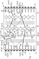
- Figure 1 shows a top view of a schematic depiction of an integrated optical circuit 110 according to the present invention.
- the integrated optical circuit 110 here comprises an optically transparent material with a first refractive index n 1 , in particular, glass or quartz, as a substrate 112.
- the substrate 112 comprises two sides 114, 114' arranged opposite to each other, wherein each side 114, 114' is equipped with eleven fiber connectors 116, wherein each connector 116 may serve as a reception 116 which may be connected with an external connector 118, in particular an optical fiber.
- two of the receptions 116 may serve as an input port 120, 120' whereas two others of the receptions 116 may serve as an output port 122, 122'.
- the receptions 116 may also be adapted to receive other kinds of external connectors 118 beside optical fibers, such as electrical connectors.
- optical fibers are preferred as the external connectors 118.
- each reception 116 is attached to a connector waveguide 124 as located on the substrate 112.
- Each connector waveguide 124 may be created in the same manner as a nanophotonic waveguide 116 as described above and/or below.
- the particular example of the integrated optical circuit 110 as depicted in Figure 1 comprises various kinds of nanophotonic waveguides 116.
- the connector waveguides 124 Beside the connector waveguides 124 as already mentioned, it further comprises nanophotonic waveguides 126, 128 being attached to a nanophotonic component 130, nanophotonic waveguides 126, 132 being in the vicinity of the nanophotonic component 130, or additional nanophotonic waveguides 126, 134 which are neither attached to the nanophotonic component 130 nor located in its vicinity.
- the nanophotonic waveguides 126 irrespective of their specific location on the substrate 112 of the integrated optical circuit 110, the nanophotonic waveguides 126 as well as the photonic components 130 comprise a material with a second refractive index n 2 , wherein the second refractive index n 2 exceeds the first refractive index n 1 of the optically transparent material as comprised by the substrate 112 as follows: n 2 > n 1
- a particularly suitable material are III-nitride semiconductors, preferably silicon nitride or aluminum nitride, or, if only infra-red wavelengths may travel along the waveguides, silicon.
- Both the nanophotonic waveguides 126 as well as the nanophotonic components 130 are made, according to the present invention, preferably from a layer of the material with the second refractive index n 2 which is placed, preferably by a known deposition technique, on top of the substrate and in which both the nanophotonic waveguides 126 and the nanophotonic components 130 are inscribed, thus, allowing or assembling many different nanophotonic waveguides 126 as well as a plurality of nanophotonic components 130 on the same substrate 112.
- Figure 2 schematically depicts a nanophotonic waveguide 126 which may be used for any of the waveguiding purposes as described above and/or below.
- Figure 2b shows a schematic view of a ring resonator 136 which may, for example, preferably be used as an optical filter.
- the optical filter 136 may be located in the vicinity of the nanophotonic waveguide 126, only separated by a comparatively short distance 138.
- the distance 138 may be selected in a manner to allow an evanescent electrical near-field to migrate between the ring resonator 136 and the corresponding nanophotonic waveguide 126 in any of the two possible directions.
- the distance 138 thus, enables an electromagnetic connection between the ring resonator 136 as the nanophotonic component 130 and the nanophotonic waveguide 126 which are placed in the vicinity with respect to each other.
- a directional coupler 140 is presented as a further example of the nanophotonic component 130.
- the directional coupler 140 may be used as a beam splitter, thus, allowing a single incident light beam to further travel into at least two separate directions.
- Figure 2d presents a Mach-Zehnder interferometer 142 which may, for example, be applied as a phase-sensitive element, thus, allowing to adjust a further transport of an incident electromagnetic wave to depend on its relative phase.
- further nanophotonic components 130 may also be arranged on the substrate 112 of the integrated optical circuit 110.
- Figure 1 schematically exhibits a particular advantage of the present invention.
- the nanophotonic components 130 as well as the additional nanophotonic waveguides 134 may be provided as many copies which may each be arranged next to each other in a form of a set or library 144, wherein the elements of each set 144 may be produced with the same but also with varying device parameters, such as a diameter 146 of the ring resonator 136.
- a specific nanophotonic component 130 which might be adapted for any desire or need, such as providing a number of different ring resonators 136 with different diameters 146 as a wide range of filter configurations an end user may be able to choose from.
- each of the nanophotonic waveguides 126 comprises two ends 148, 148', wherein in the example according to Figure 1 , where all nanophotonic waveguides 126 have been produced in manner that they are parallel to each other, the first or left ends are denoted by the reference number 148 whereas the second or right ends are denoted by the reference number 148'.
- the first or left ends are denoted by the reference number 148 whereas the second or right ends are denoted by the reference number 148'.
- other configurations may be possible.
- the integrated optical circuit 110 comprises a number of photonic wires 150 being configured to connect at least one of the connector waveguides 124 to at least one nanophotonic waveguide 126 as comprised on the substrate 112.
- a first chain of connections between the first input port 120 and the first output port 122 as well as a second chain of connections between the second input port 120' and the second output port 122' are schematically presented.
- the right end 148' of the connector waveguide 124 attached to the first input port 120 of the reception 116 is connected by a photonic wire 150 to the left end 148 of a nanophotonic waveguide 126, 128 attached to the nanophotonic component 130, in this example comprising a phase-sensitive Mach-Zehnder interferometer 142.
- a further nanowire 150 leads to the left end 148 of the connector waveguide 124 attached to the first output port 122 at a reception 116.
- This exemplary chain of connections from the first input port 120 to the second output port 122 thus, constitutes an uninterrupted path which comprises various constituents, i.e. the connector waveguides 124, the nanophotonic waveguides 126, and the nanophotonic components 130, as provided by the nanophotonic device, and, additionally, the photonic wires 150 which, thus, accomplish the first chain of connections on the integrated optical circuit 110.
- the photonic wire 150 comprises a polymer waveguide which is located above the top 152 of the substrate 112.
- such polymer waveguides may, in particular, be written at arbitrary positions by using the technique of direct-laser writing. Since direct-laser writing may provide access to the third dimension above the top 152 of the substrate 112, waveguide cross-overs and long-range connections between distant waveguides may, thus, be provided, thus providing features which are impossible within known planar devices.
- at the waveguides 126 may be equipped with a tapering section 154 at both of their ends 148, 148'.
- the tapering sections 154 at the ends 148, 148' of the nanophotonic waveguides 126 force an optical mode travelling along a specific nanophotonic waveguide 126 to become enlarged.
- an efficient coupling of the optical mode as provided by the nanophotonic waveguide 126 to the photonic wire 150 attached to it may, thus, achieved.
- optimized tapering sections 154 may be fabricated in a manner that the same kind of photonic wires 150 may be used for different nanophotonic waveguides 126 at least of the same dimensions.
- a more complex second chain of connections from the second input port 120' to the second output port 122' may be achieved by employing the integrated optical circuit according to the present invention.
- an incident light wave provided by the optical fiber as external connector 118 to the fiber connector reception 116 of the integrated optical circuit 110, which functions as the second input port 120' of the present integrated optical circuit 110 may travel via the additional nanophotonic waveguide 134 to the nanophotonic waveguide 126, 132 located in the vicinity of the ring resonator 136 as the nanophotonic component 130, via a further nanophotonic waveguide 126, 128 attached to the phase-sensitive Mach-Zehnder interferometer 142 as a further nanophotonic component 130, via another nanophotonic waveguide 126, 128 attached to a further phase-sensitive Mach-Zehnder interferometer 142 as a further nanophotonic component 130 to the further connector waveguide 124 attached to the second output port 122', from where an optical signal
- a particular advantage of the integrated optical circuit 110 according to the present invention comprises the fact that the integrated optical circuit 110 may, nevertheless, be modified in a rather flexible way after its manufacturing. It may still be possible, for example by employing a plasma oxidation, to remove one or more of the photonic wires 150 as shown in Figure 1 and, if required to further provide new photonic wires 150 by using direct-laser writing as described above. Consequently, the present invention provides a reconfigurable integrated optical circuit 110 which may be used as a rewritable integrated optical circuit, such as according to the specific desires or requirements of the end user.
Landscapes
- Physics & Mathematics (AREA)
- General Physics & Mathematics (AREA)
- Optics & Photonics (AREA)
- Engineering & Computer Science (AREA)
- Microelectronics & Electronic Packaging (AREA)
- Optical Integrated Circuits (AREA)
Claims (7)
- Verfahren zum Herstellen und Rekonfigurieren einer integrierten optischen Schaltung (110), wobei die integrierte optische Schaltung (110)- mindestens eine nanophotonische Vorrichtung umfasst, die ein Substrat (112) umfasst, wobei das Substrat (112) mit mindestens einer Aufnahme (116) für mindestens einen externen Verbinder (118) ausgestattet ist, wobei die Aufnahme (116) mit mindestens einem Verbinderwellenleiter (124) gekoppelt ist, ferner umfassend mindestens einen Satz von nanooptischen Komponenten, wobei die nanooptische Komponente eine nanophotonische Komponente (130) ist, wobei die nanophotonische Komponente (130) nanooptisch an mindestens einen nanophotonischen Wellenleiter (126) gekoppelt ist, wobei mindestens einer von den nanophotonischen Wellenleitern (126) selektiv mit mindestens einem der Verbinderwellenleiter (124) koppelbar ist, wobei sich "selektiv" auf das Koppeln jeweiliger Enden der nanophotonischen Wellenleiter bezieht, wie sie auf dem Substrat vorhanden sind oder nicht;- ferner mindestens einen photonischen Draht (150) umfasst, wobei der photonische Draht (150) mindestens einen der nanophotonischen Wellenleiter (126) mit mindestens einem der Verbinderwellenleiter (124) verbindet,wobei das Substrat (112) teilweise durch eine Schutzschicht bedeckt ist, wobei sich die Schutzschicht außerhalb eines Bereichs auf dem Substrat (112) erstreckt, in dem sich mindestens einer der photonischen Drähte (150) befindet, wobei das Verfahren die folgenden Schritte umfasst:(a) Bereitstellen eines Substrats (112), wobei das Substrat (112) mit mindestens einer Aufnahme (116) für mindestens einen externen Verbinder (118) ausgestattet ist, wobei die Aufnahme (116) mit mindestens einem Verbinderwellenleiter (124) gekoppelt ist;(b) Platzieren einer Schicht eines Materials auf dem Substrat (112);(c) Erzeugen mindestens eines Satzes von nanooptischen Komponenten innerhalb der Schicht des Materials, die auf dem Substrat (112) platziert ist, wobei die nanooptische Komponente eines von einem nanophotonischen Wellenleiter (126) oder einer nanophotonischen Komponente (130) ist, wobei die nanophotonische Komponente (130) nanooptisch mit mindestens einem nanophotonischen Wellenleiter (126) gekoppelt ist, wobei mindestens einer der nanophotonischen Wellenleiter (126) selektiv mit mindestens einer der Verbinderwellenleiter (124) koppelbar ist; und(d) Bereitstellen mindestens eines photonischen Drahts (150), wobei der photonische Draht (150) mindestens einen der Verbinderwellenleiter (124) mit mindestens einem der nanophotonischen Wellenleiter (126) verbindet;wobei nach Schritt (d) mindestens einer der photonischen Drähte (150), die in der integrierten optischen Schaltung (110) enthalten sind, entfernt wird, und wobei mindestens ein weiterer photonischer Draht (150) in der integrierten optischen Schaltung (110) bereitgestellt wird,wobei der photonische Draht (150) durch photonisches Drahtbonden unter Verwendung von direktem Laserschreiben innerhalb eines Polymermaterials bereitgestellt wird,wobei der photonische Draht (150) einen Polymerwellenleiter umfasst, wobei sich der Polymerwellenleiter über dem Substrat (112) befindet.
- Verfahren nach dem vorhergehenden Verfahrensanspruch, wobei eine nanooptische Kopplung der nanophotonischen Komponente (130) mit dem mindestens einen nanophotonischen Wellenleiter (126) durch eines von Befestigen der nanophotonischen Komponente (130) an dem mindestens einen nanophotonischen Wellenleiter (126, 128) oder Lokalisieren der nanophotonischen Komponente (130) in der Nähe des mindestens einen nanophotonischen Wellenleiters (126, 132) erhalten wird.
- Verfahren nach einem der vorhergehenden Verfahrensansprüche, wobei die nanophotonische Komponente (130) aus einer Gruppe ausgewählt ist, die einen Ringresonator (136), einen Richtkoppler (140) und ein phasenempfindliches Element (142) umfasst.
- Verfahren nach einem der vorhergehenden Verfahrensansprüche, wobei eine Vielzahl von nanooptischen Komponenten, wobei sich mindestens zwei der nanooptischen Komponenten innerhalb des Satzes in Bezug auf mindestens eine Eigenschaft unterscheiden, als der Satz von nanooptischen Komponenten erzeugt wird.
- Verfahren nach einem der vorhergehenden Verfahrensansprüche, wobei eine Kette von Verbindungen von mindestens einem Eingangsport (120, 120') zu mindestens einem Ausgangsport (122, 122') unter Verwendung von mindestens zwei photonischen Drähten (150) bereitgestellt wird, wobei einer der photonischen Drähte (150) den Verbinderwellenleiter (124), der mit dem Eingangsport (120, 120') gekoppelt ist, mit einem der nanophotonischen Wellenleiter (126) verbindet, und wobei ein anderer der photonischen Drähte (150) den nanophotonischen Wellenleiter (126) oder einen weiteren nanophotonischen Wellenleiter (126), der nanooptisch mit der gleichen nanophotonischen Komponente (130) gekoppelt ist, mit dem Verbinderwellenleiter (124) verbindet, der mit dem Ausgangsport (122, 122') gekoppelt ist.
- Verfahren nach einem der vorhergehenden Verfahrensansprüche, ferner umfassend den folgenden Schritt:
(e) teilweises Bedecken des Substrats (112) mit einer Schutzschicht auf eine Weise, dass sich die Schutzschicht außerhalb eines Bereichs des Substrats (112) erstreckt, in dem sich die mindestens zwei photonischen Drähte (150) befinden. - Verfahren nach einem der vorhergehenden Verfahrensansprüche, wobei der mindestens eine photonische Draht (150) einen Polymerwellenleiter umfasst, der durch eine Plasmaoxidation entfernt wird.
Priority Applications (2)
| Application Number | Priority Date | Filing Date | Title |
|---|---|---|---|
| EP14166424.3A EP2940500B1 (de) | 2014-04-29 | 2014-04-29 | Integrierte optische schaltung und verfahren zu deren herstellung und rekonfiguration |
| US14/698,551 US9678278B2 (en) | 2014-04-29 | 2015-04-28 | Integrated optical circuit and methods for its manufacturing and reconfiguring |
Applications Claiming Priority (1)
| Application Number | Priority Date | Filing Date | Title |
|---|---|---|---|
| EP14166424.3A EP2940500B1 (de) | 2014-04-29 | 2014-04-29 | Integrierte optische schaltung und verfahren zu deren herstellung und rekonfiguration |
Publications (3)
| Publication Number | Publication Date |
|---|---|
| EP2940500A1 EP2940500A1 (de) | 2015-11-04 |
| EP2940500C0 EP2940500C0 (de) | 2025-03-26 |
| EP2940500B1 true EP2940500B1 (de) | 2025-03-26 |
Family
ID=50687263
Family Applications (1)
| Application Number | Title | Priority Date | Filing Date |
|---|---|---|---|
| EP14166424.3A Active EP2940500B1 (de) | 2014-04-29 | 2014-04-29 | Integrierte optische schaltung und verfahren zu deren herstellung und rekonfiguration |
Country Status (2)
| Country | Link |
|---|---|
| US (1) | US9678278B2 (de) |
| EP (1) | EP2940500B1 (de) |
Families Citing this family (5)
| Publication number | Priority date | Publication date | Assignee | Title |
|---|---|---|---|---|
| WO2018022319A1 (en) * | 2016-07-29 | 2018-02-01 | Corning Optical Communications LLC | Waveguide connector elements and optical assemblies incorporating the same |
| LU101084B1 (de) * | 2018-12-21 | 2020-06-22 | Abberior Instruments Gmbh | Verfahren und Vorrichtung zum punktförmigen Beleuchten einer Probe in einem Mikroskiop |
| KR102739799B1 (ko) * | 2021-01-27 | 2024-12-10 | 한국전자통신연구원 | 이종 집적 광 변조기 및 그의 제조 방법 |
| CN112925073B (zh) * | 2021-02-09 | 2022-04-22 | 中国科学院半导体研究所 | 光电子集成器件的光互联方法 |
| CN115987396A (zh) * | 2022-12-09 | 2023-04-18 | 中国科学院半导体研究所 | 基于光子引线键合的可编程集成光芯片 |
Family Cites Families (8)
| Publication number | Priority date | Publication date | Assignee | Title |
|---|---|---|---|---|
| US6035080A (en) * | 1997-06-20 | 2000-03-07 | Henry; Charles Howard | Reconfigurable add-drop multiplexer for optical communications systems |
| US6658179B2 (en) * | 2001-11-08 | 2003-12-02 | Xerox Corporation | Monolithic reconfigurable optical multiplexer systems and methods |
| US7894418B2 (en) * | 2002-08-15 | 2011-02-22 | The Boeing Company | Mixed analog and digital chip-scale reconfigurable WDM network |
| US6723573B2 (en) * | 2002-08-16 | 2004-04-20 | Sarnoff Corporation | Photonic devices and PICs including sacrificial testing structures and method of making the same |
| WO2006138587A2 (en) * | 2005-06-18 | 2006-12-28 | The Regents Of The University Of Colorado, A Body Corporate | Three-dimensional direct-write lithography |
| US9034222B2 (en) * | 2012-02-23 | 2015-05-19 | Karlsruhe Institut Fuer Technologie | Method for producing photonic wire bonds |
| US8903205B2 (en) | 2012-02-23 | 2014-12-02 | Karlsruhe Institute of Technology (KIT) | Three-dimensional freeform waveguides for chip-chip connections |
| US9478842B1 (en) * | 2015-03-16 | 2016-10-25 | The United States Of America As Represented By The Administrator Of The National Aeronautics And Space Administration | Interconnect between a waveguide and a dielectric waveguide comprising an impedance matched dielectric lens |
-
2014
- 2014-04-29 EP EP14166424.3A patent/EP2940500B1/de active Active
-
2015
- 2015-04-28 US US14/698,551 patent/US9678278B2/en active Active
Also Published As
| Publication number | Publication date |
|---|---|
| US20150309260A1 (en) | 2015-10-29 |
| EP2940500A1 (de) | 2015-11-04 |
| EP2940500C0 (de) | 2025-03-26 |
| US9678278B2 (en) | 2017-06-13 |
Similar Documents
| Publication | Publication Date | Title |
|---|---|---|
| WO2016131355A1 (en) | Photonic chip surface grating coupler (sgc) -based optical splitter and optical combiner | |
| Gehring et al. | Low-loss fiber-to-chip couplers with ultrawide optical bandwidth | |
| US10317625B2 (en) | Polymer waveguide (PWG) connector assembly having both cores and cladding partially exposed | |
| US9678278B2 (en) | Integrated optical circuit and methods for its manufacturing and reconfiguring | |
| US9482816B2 (en) | Radiation coupler | |
| US8594503B2 (en) | Method and system for multiplexer waveguide coupling | |
| US7474825B1 (en) | Circular grating resonator with integrated electro-optical modulation | |
| US6915029B2 (en) | High density integrated optical chip with low index difference and high index difference waveguide functions | |
| JP2015191110A (ja) | 光導波路結合構造および光導波路結合構造の製造方法 | |
| JP2006525556A (ja) | 面外導波路を使用する低損失光導波路クロスオーバ | |
| US8705920B2 (en) | Wavelength filter | |
| US20210263219A1 (en) | Planar Lightwave Circuit and Optical Device | |
| WO2001023955A2 (en) | A nanophotonic mach-zehnder interferometer switch and filter | |
| JP3552592B2 (ja) | 光導波路の製造方法 | |
| US7983514B2 (en) | Photonic band gap router | |
| JP2005010333A (ja) | 導波路型光信号処理器 | |
| EP4441539A1 (de) | Photonische integrierte schaltungen | |
| US20140056552A1 (en) | Optical path routing element | |
| Bogaerts et al. | Silicon nanophotonic waveguides and their applications | |
| US7995891B2 (en) | Photonic band gap router | |
| JP4091944B2 (ja) | 光回路 | |
| US7639900B2 (en) | Photonic band gap router | |
| EP4285169B1 (de) | Photonische integrierte schaltung | |
| US20080089639A1 (en) | Photonic band gap router | |
| Kaźmierczak et al. | Analysis of silicon on insulator (SOI) optical microring add-drop filter based on waveguide intersections |
Legal Events
| Date | Code | Title | Description |
|---|---|---|---|
| PUAI | Public reference made under article 153(3) epc to a published international application that has entered the european phase |
Free format text: ORIGINAL CODE: 0009012 |
|
| AK | Designated contracting states |
Kind code of ref document: A1 Designated state(s): AL AT BE BG CH CY CZ DE DK EE ES FI FR GB GR HR HU IE IS IT LI LT LU LV MC MK MT NL NO PL PT RO RS SE SI SK SM TR |
|
| AX | Request for extension of the european patent |
Extension state: BA ME |
|
| RIN1 | Information on inventor provided before grant (corrected) |
Inventor name: BLAICHER, MATTHIAS Inventor name: WEGENER, MARTIN Inventor name: PERNICE, WOLFRAM |
|
| 17P | Request for examination filed |
Effective date: 20160405 |
|
| RBV | Designated contracting states (corrected) |
Designated state(s): AL AT BE BG CH CY CZ DE DK EE ES FI FR GB GR HR HU IE IS IT LI LT LU LV MC MK MT NL NO PL PT RO RS SE SI SK SM TR |
|
| STAA | Information on the status of an ep patent application or granted ep patent |
Free format text: STATUS: EXAMINATION IS IN PROGRESS |
|
| 17Q | First examination report despatched |
Effective date: 20190425 |
|
| GRAP | Despatch of communication of intention to grant a patent |
Free format text: ORIGINAL CODE: EPIDOSNIGR1 |
|
| STAA | Information on the status of an ep patent application or granted ep patent |
Free format text: STATUS: GRANT OF PATENT IS INTENDED |
|
| INTG | Intention to grant announced |
Effective date: 20241022 |
|
| RAP3 | Party data changed (applicant data changed or rights of an application transferred) |
Owner name: KARLSRUHER INSTITUT FUER TECHNOLOGIE |
|
| GRAS | Grant fee paid |
Free format text: ORIGINAL CODE: EPIDOSNIGR3 |
|
| GRAA | (expected) grant |
Free format text: ORIGINAL CODE: 0009210 |
|
| STAA | Information on the status of an ep patent application or granted ep patent |
Free format text: STATUS: THE PATENT HAS BEEN GRANTED |
|
| AK | Designated contracting states |
Kind code of ref document: B1 Designated state(s): AL AT BE BG CH CY CZ DE DK EE ES FI FR GB GR HR HU IE IS IT LI LT LU LV MC MK MT NL NO PL PT RO RS SE SI SK SM TR |
|
| REG | Reference to a national code |
Ref country code: GB Ref legal event code: FG4D |
|
| REG | Reference to a national code |
Ref country code: CH Ref legal event code: EP |
|
| REG | Reference to a national code |
Ref country code: DE Ref legal event code: R096 Ref document number: 602014091718 Country of ref document: DE |
|
| REG | Reference to a national code |
Ref country code: IE Ref legal event code: FG4D |
|
| U01 | Request for unitary effect filed |
Effective date: 20250416 |
|
| U07 | Unitary effect registered |
Designated state(s): AT BE BG DE DK EE FI FR IT LT LU LV MT NL PT RO SE SI Effective date: 20250424 |
|
| PG25 | Lapsed in a contracting state [announced via postgrant information from national office to epo] |
Ref country code: RS Free format text: LAPSE BECAUSE OF FAILURE TO SUBMIT A TRANSLATION OF THE DESCRIPTION OR TO PAY THE FEE WITHIN THE PRESCRIBED TIME-LIMIT Effective date: 20250626 |
|
| PG25 | Lapsed in a contracting state [announced via postgrant information from national office to epo] |
Ref country code: NO Free format text: LAPSE BECAUSE OF FAILURE TO SUBMIT A TRANSLATION OF THE DESCRIPTION OR TO PAY THE FEE WITHIN THE PRESCRIBED TIME-LIMIT Effective date: 20250626 |
|
| PG25 | Lapsed in a contracting state [announced via postgrant information from national office to epo] |
Ref country code: HR Free format text: LAPSE BECAUSE OF FAILURE TO SUBMIT A TRANSLATION OF THE DESCRIPTION OR TO PAY THE FEE WITHIN THE PRESCRIBED TIME-LIMIT Effective date: 20250326 |
|
| U20 | Renewal fee for the european patent with unitary effect paid |
Year of fee payment: 12 Effective date: 20250606 |
|
| PG25 | Lapsed in a contracting state [announced via postgrant information from national office to epo] |
Ref country code: GR Free format text: LAPSE BECAUSE OF FAILURE TO SUBMIT A TRANSLATION OF THE DESCRIPTION OR TO PAY THE FEE WITHIN THE PRESCRIBED TIME-LIMIT Effective date: 20250627 |
|
| PG25 | Lapsed in a contracting state [announced via postgrant information from national office to epo] |
Ref country code: SM Free format text: LAPSE BECAUSE OF FAILURE TO SUBMIT A TRANSLATION OF THE DESCRIPTION OR TO PAY THE FEE WITHIN THE PRESCRIBED TIME-LIMIT Effective date: 20250326 |
|
| PG25 | Lapsed in a contracting state [announced via postgrant information from national office to epo] |
Ref country code: ES Free format text: LAPSE BECAUSE OF FAILURE TO SUBMIT A TRANSLATION OF THE DESCRIPTION OR TO PAY THE FEE WITHIN THE PRESCRIBED TIME-LIMIT Effective date: 20250326 |
|
| PG25 | Lapsed in a contracting state [announced via postgrant information from national office to epo] |
Ref country code: PL Free format text: LAPSE BECAUSE OF FAILURE TO SUBMIT A TRANSLATION OF THE DESCRIPTION OR TO PAY THE FEE WITHIN THE PRESCRIBED TIME-LIMIT Effective date: 20250326 |
|
| PG25 | Lapsed in a contracting state [announced via postgrant information from national office to epo] |
Ref country code: SK Free format text: LAPSE BECAUSE OF FAILURE TO SUBMIT A TRANSLATION OF THE DESCRIPTION OR TO PAY THE FEE WITHIN THE PRESCRIBED TIME-LIMIT Effective date: 20250326 |
|
| PG25 | Lapsed in a contracting state [announced via postgrant information from national office to epo] |
Ref country code: IS Free format text: LAPSE BECAUSE OF FAILURE TO SUBMIT A TRANSLATION OF THE DESCRIPTION OR TO PAY THE FEE WITHIN THE PRESCRIBED TIME-LIMIT Effective date: 20250726 |
|
| REG | Reference to a national code |
Ref country code: CH Ref legal event code: H13 Free format text: ST27 STATUS EVENT CODE: U-0-0-H10-H13 (AS PROVIDED BY THE NATIONAL OFFICE) Effective date: 20251125 |
|
| PG25 | Lapsed in a contracting state [announced via postgrant information from national office to epo] |
Ref country code: MC Free format text: LAPSE BECAUSE OF FAILURE TO SUBMIT A TRANSLATION OF THE DESCRIPTION OR TO PAY THE FEE WITHIN THE PRESCRIBED TIME-LIMIT Effective date: 20250326 |
|
| PG25 | Lapsed in a contracting state [announced via postgrant information from national office to epo] |
Ref country code: CH Free format text: LAPSE BECAUSE OF NON-PAYMENT OF DUE FEES Effective date: 20250430 |
|
| PG25 | Lapsed in a contracting state [announced via postgrant information from national office to epo] |
Ref country code: CZ Free format text: LAPSE BECAUSE OF FAILURE TO SUBMIT A TRANSLATION OF THE DESCRIPTION OR TO PAY THE FEE WITHIN THE PRESCRIBED TIME-LIMIT Effective date: 20250326 |
|
| PLBE | No opposition filed within time limit |
Free format text: ORIGINAL CODE: 0009261 |
|
| STAA | Information on the status of an ep patent application or granted ep patent |
Free format text: STATUS: NO OPPOSITION FILED WITHIN TIME LIMIT |
|
| REG | Reference to a national code |
Ref country code: CH Ref legal event code: L10 Free format text: ST27 STATUS EVENT CODE: U-0-0-L10-L00 (AS PROVIDED BY THE NATIONAL OFFICE) Effective date: 20260211 |
|
| GBPC | Gb: european patent ceased through non-payment of renewal fee |
Effective date: 20250626 |
|
| 26N | No opposition filed |
Effective date: 20260105 |
|
| PG25 | Lapsed in a contracting state [announced via postgrant information from national office to epo] |
Ref country code: GB Free format text: LAPSE BECAUSE OF NON-PAYMENT OF DUE FEES Effective date: 20250626 |
|
| PG25 | Lapsed in a contracting state [announced via postgrant information from national office to epo] |
Ref country code: IE Free format text: LAPSE BECAUSE OF NON-PAYMENT OF DUE FEES Effective date: 20250429 |