EP2940592B1 - Circuit d'excursion basse pour un appareil - Google Patents
Circuit d'excursion basse pour un appareil Download PDFInfo
- Publication number
- EP2940592B1 EP2940592B1 EP15160427.9A EP15160427A EP2940592B1 EP 2940592 B1 EP2940592 B1 EP 2940592B1 EP 15160427 A EP15160427 A EP 15160427A EP 2940592 B1 EP2940592 B1 EP 2940592B1
- Authority
- EP
- European Patent Office
- Prior art keywords
- line
- power
- cable
- pull
- configuration
- Prior art date
- Legal status (The legal status is an assumption and is not a legal conclusion. Google has not performed a legal analysis and makes no representation as to the accuracy of the status listed.)
- Active
Links
Images



Classifications
-
- G—PHYSICS
- G05—CONTROLLING; REGULATING
- G05F—SYSTEMS FOR REGULATING ELECTRIC OR MAGNETIC VARIABLES
- G05F3/00—Non-retroactive systems for regulating electric variables by using an uncontrolled element, or an uncontrolled combination of elements, such element or such combination having self-regulating properties
- G05F3/02—Regulating voltage or current
-
- G—PHYSICS
- G06—COMPUTING OR CALCULATING; COUNTING
- G06F—ELECTRIC DIGITAL DATA PROCESSING
- G06F13/00—Interconnection of, or transfer of information or other signals between, memories, input/output devices or central processing units
- G06F13/38—Information transfer, e.g. on bus
- G06F13/40—Bus structure
- G06F13/4063—Device-to-bus coupling
- G06F13/409—Mechanical coupling
-
- H—ELECTRICITY
- H01—ELECTRIC ELEMENTS
- H01R—ELECTRICALLY-CONDUCTIVE CONNECTIONS; STRUCTURAL ASSOCIATIONS OF A PLURALITY OF MUTUALLY-INSULATED ELECTRICAL CONNECTING ELEMENTS; COUPLING DEVICES; CURRENT COLLECTORS
- H01R13/00—Details of coupling devices of the kinds covered by groups H01R12/70 or H01R24/00 - H01R33/00
- H01R13/66—Structural association with built-in electrical component
- H01R13/665—Structural association with built-in electrical component with built-in electronic circuit
-
- H—ELECTRICITY
- H01—ELECTRIC ELEMENTS
- H01R—ELECTRICALLY-CONDUCTIVE CONNECTIONS; STRUCTURAL ASSOCIATIONS OF A PLURALITY OF MUTUALLY-INSULATED ELECTRICAL CONNECTING ELEMENTS; COUPLING DEVICES; CURRENT COLLECTORS
- H01R13/00—Details of coupling devices of the kinds covered by groups H01R12/70 or H01R24/00 - H01R33/00
- H01R13/66—Structural association with built-in electrical component
- H01R13/70—Structural association with built-in electrical component with built-in switch
-
- Y—GENERAL TAGGING OF NEW TECHNOLOGICAL DEVELOPMENTS; GENERAL TAGGING OF CROSS-SECTIONAL TECHNOLOGIES SPANNING OVER SEVERAL SECTIONS OF THE IPC; TECHNICAL SUBJECTS COVERED BY FORMER USPC CROSS-REFERENCE ART COLLECTIONS [XRACs] AND DIGESTS
- Y02—TECHNOLOGIES OR APPLICATIONS FOR MITIGATION OR ADAPTATION AGAINST CLIMATE CHANGE
- Y02D—CLIMATE CHANGE MITIGATION TECHNOLOGIES IN INFORMATION AND COMMUNICATION TECHNOLOGIES [ICT], I.E. INFORMATION AND COMMUNICATION TECHNOLOGIES AIMING AT THE REDUCTION OF THEIR OWN ENERGY USE
- Y02D10/00—Energy efficient computing, e.g. low power processors, power management or thermal management
Definitions
- the embodiments relate to an apparatus or dual-role port capability to request power via a wired interface.
- Serial and parallel communication interfaces are widely used to establish communication between devices such as desktop computers and printers, stationary terminals and peripheral devices, personal computers, mobile terminals, and headsets.
- devices such as desktop computers and printers, stationary terminals and peripheral devices, personal computers, mobile terminals, and headsets.
- USB universal serial bus
- USB ports and cables supply both data and electric power, enabling power consumer devices needing operating power, to obtain their operating power via the USB cable from a power provider device.
- the power provider devices may also include mains adapters or car chargers without data communication capabilities.
- WO 2008/146073 A1 discloses a method comprising connecting an electronic device having a power source with a second electronic device via a wired interface comprising a first data line and a voltage line, turning off power provided to said voltage line, monitoring the voltage level of said first data line, and determining that said second electronic device has been disconnected if a change from high level to low level is detected.
- a second method comprising connecting an electronic device with a first electronic device via a wired interface comprising a second data line and a voltage line, connecting a second pull -down resistor with said second data line, monitoring said voltage line, disconnecting said second pull -down resistor from said second data line and connecting a second pull-up resistor with said second data line if power provided on said voltage line is turned off, monitoring a voltage level of said second data line, and determining that said first electronic device has been disconnected if a change from low level to high level is detected.
- US 2008/247104 A1 discloses an electrostatic discharge protection circuit.
- the disclosed electrostatic discharge protection circuit includes a transfer unit that transfers electrostaticity from at least one of a plurality of input/output pads to a boost bus line, a trigger unit that responds to the electrostaticity transferred via the boost bus line to detect a trigger voltage and apply it to a trigger bus line, and a plurality of clamp units that are connected between the input/output pads and an internal circuit.
- the clamp units are triggered by the trigger voltage of the trigger unit to discharge electrostaticity of the input/output pads to a first or second power supply voltage line, thereby safely protecting the internal circuit from electrostatic damage and lowering the operating voltage of the clamp unit with minimum costs without increasing an area of the electrostatic discharge protective circuit within a semiconductor integrated circuit.
- Apparatus embodiments of the invention are disclosed for requesting power via a wired interface.
- an apparatus comprises:
- an apparatus comprises:
- an apparatus comprises:
- an apparatus comprises:
- an apparatus comprises:
- an apparatus comprises:
- an apparatus comprises:
- an apparatus comprises:
- an apparatus comprises:
- an apparatus comprises:
- an apparatus comprises:
- an apparatus comprises:
- embodiments of the invention enable requesting power via a wired interface.
- a USB system may include a host, a plurality of downstream USB ports, and a plurality of peripheral devices connected in a tiered-star topology. Additional USB hubs may be included in the tiers, allowing branching into a tree structure with up to five tier levels.
- a USB host may have multiple host controllers and each host controller may provide one or more USB ports. Up to 127 devices, including hub devices, may be connected to a single host controller.
- a new USB Type-C connector is an interface supporting the USB 3.0 level of communication.
- the USB Type-C connector features a Dual-Role Port that can operate as either a Downstream Facing Port (DFP) or an Upstream Facing Port (UFP).
- a Downstream Facing Port typically the ports on a host or the ports on a hub to which devices are connected.
- An Upstream Facing Port is a port on a device or a hub that connects to a host or the Downstream Facing Port of a hub.
- the role that the port offers may be fixed to either a Downstream Facing Port (DFP) or an Upstream Facing Port (UFP) or may alternate between the two port states. The port's role may be changed dynamically.
- the USB Type-C connector is symmetrical so that it may be plugged in both ways, up-side- up or up-side-down.
- the polarity of the plug and power provider/power consumer role will be configured by a system called Configuration Channel (CC), which has two pins CC1 and CC2 at each receptacle, but only one of them, CC1, is wired trough the cable from the plugs.
- CC Configuration Channel
- Both Configuration Channel (CC)-pins are pulled up in the power provider side and pulled down in the power consumer side by resistors.
- both may monitor both of the Configuration Channel (CC)-pins and see that at both ends only one pin will change its voltage level. Noting which pin this is, the power provider or device may negotiate which way the plug is inserted locally. After the valid connection is detected, a +5 V VCONN voltage or voltage supply is applied to the unused CC-pin for possible active cables.
- a single connector line may be used as either the power source or the power sink.
- the power provider and power consumer devices must negotiate this the direction of power at the time of setup. For this negotiation, the device that is to consume power, pulls the voltage of the Configuration Channel (CC) connector line low at the time when galvanic connection between connector contacts is established. This lowering of the voltage in the Configuration Channel (CC) line is detected by the power provider device, thereby establishing their respective roles.
- CC Configuration Channel
- a Dual-Role Port device without power or with a dead battery needs to act as a power consumer device at setup time, to be able to get charging power from a power provider device or host via the VBUS.
- the Dual-Role Port needs to pull the Configuration Channel (CC) line below 1.8V and above 0.4V.
- a semiconductor switch in the Dual-Role Port device acting as a power consumer would not be able to connect the Configuration Channel (CC) line to a low voltage level, without having proper operating voltage.
- Figure 1A illustrates an example functional block diagram of a power provider device 102 and a Device with Dual-Role port acting as Power Consumer 104 to be connected by a cable 130, such as for example a USB cable.
- the connector 140 such as a USB Type-C connector, has an example USB Type-C connector pinning shown in Figure 1B .
- the power provider device 102 has a receptacle 120, such as for example a USB type-C receptacle to receive the connector 140 plugged into the receptacle 120.
- the figure shows the pull-down circuit 300 in the Device with Dual-Role port acting as Power Consumer 104, in accordance with an example embodiment of the invention.
- the power provider device 102 may include processing logic 222 that may include one or several central processor units (CPUs) 224 and 225, a random-access memory (RAM) 226, and a read-only memory (ROM) 227.
- processing logic 222 may include programmed logic arrays of sequential and combinatorial logic circuits and state machine logic implementing some or all of the steps performed by embodiments of the invention.
- the source protocol 112 may be embodied as a programmed sequence of executable instructions stored in the RAM or ROM and executed by the central processor unit (CPU) to carry out the functions of embodiments of the invention.
- Power Consumer 104 is an apparatus acting as a power consumer when there is no energy in the apparatus. This means that it may be in a power down mode, or that it may have an empty battery, or that it may have no battery.
- FIG. 2 illustrates an example circuit diagram of a pull-down circuit 300 in the Device with Dual-Role port acting as Power Consumer 104, in accordance with an example embodiment of the invention.
- CC Configuration Channel
- the pull-down circuit 300 in the Device with Dual-Role port acting as Power Consumer 104 uses a bit of energy from the Configuration Channel (CC) line, itself, to pull down the voltage of the Configuration Channel (CC) line, making it go down enough to trigger the power provider or host 104 to start charging the VBUS line. If the Power Consumer device 104 includes a battery that becomes charged by the power provided on the VBUS line, then in response, the pull down circuit 300 stops pulling down the voltage of the Configuration Channel line and releases control of the Configuration Channel to other circuitry having a capability for logic decisions, such as a CPU.
- CC Configuration Channel
- the pull down circuit 300 stops pulling down the voltage of the Configuration Channel line and releases control of the Configuration Channel to other circuitry having a capability for logic decisions, such as a CPU.
- the pull-down circuit 300 in the Device with Dual-Role port acting as Power Consumer 104 may be an FET circuit, transistor, relay, MEMS switch, or another type of circuit that is capable of providing the pull-down, if that device has a dead battery or no power source of its own.
- Example embodiments of the invention may be more generally applied to power interfaces where the power consumer requests power by pulling a line low, where the device has its own power off or when its battery is empty.
- the N-channel FET2 has its gate coupled through a resistor R2 to the Configuration Channel (CC) line of the USB-Type C cable, its source connected to ground potential, and its drain connected to the Configuration Channel (CC) line of the cable.
- the N-channel FET2 is configured to become more conductive, reducing voltage on the Configuration Channel (CC) line of the cable, thereby signaling the power provider device 102 over the Configuration Channel (CC) line, to provide power to the apparatus on the VBUS line of the cable.
- dual role port device 104 When dual role port device 104 is in a power off mode or has a dead battery, the device's VCONN voltage or voltage supply is not present at the gate of FET1 and the FET1 will not conduct.
- a power provider or host 102 When a power provider or host 102 is attached to this dual role port, it will apply a voltage (VCON) through a resistor to the Configuration Channel (CC) line.
- VCONN voltage or voltage supply is applied to the gate of FET2 and FET2 starts to conduct. As FET2 starts to conduct, it will draw the Configuration Channel (CC) line voltage down. At the same time the Configuration Channel (CC) line is drawing the FET2 gate voltage too low to keep FET2 conducting.
- FET2 starts to "toggle” and will keep its drain to source voltage of FET2 at approximately its threshold voltage (1.2V threshold recommended).
- This drain to source voltage of 1.2V is then detected on the Configuration Channel (CC) line by the power provider or host device 102, which indicates to the power provider or host device 102 that it should assume the role of providing power to the Device with Dual-Role port acting as Power Consumer 104, by providing charging power through the VBUS line.
- CC Configuration Channel
- the device 104 When the power provider or host 102 provides power on the VBUS line to the Device with Dual-Role port acting as Power Consumer 104, the device 104 will either power itself up (if that is its required functionality) or first start to charge its dead battery and power-up (if required) after the level of its battery charge is in a "battery good"-level. When the device 104 succeeds in powering up, it will provide its VCONN voltage or voltage supply to the gate of FET1, and when FET1 becomes conductive, it lowers the voltage on the gate of FET2, thereby turning FET2 off and raising the voltage on the Configuration Channel (CC).
- CC Configuration Channel
- the power provider or host device 102 will detect the rise in voltage on the Configuration Channel (CC) line and may reduce or stop providing power on the VBUS line to the device 104. If the device 104 has a limited amount of charge in reserve and later depletes its charge, the pull-down circuit 300, once again, will signal the power provider or host device 102 to resume providing power on the VBUS line.
- CC Configuration Channel
- Figure 2A illustrates an example circuit diagram of an N-channel FET pull-down circuit in the Device with Device-Role port acting as Power Consumer, in accordance with an example embodiment of the invention.
- the situation is same with the device-mode port devices as per USB Type-C specification.
- Those device-mode devices need to support VCONN or voltage supply for the active cables, which leads to situation that devices need to have capability to switch pull down off as well.
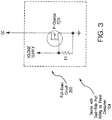
- FIG. 3 illustrates an example circuit diagram of a P-channel FET pull-down circuit 350 in the dual role port in the Device with Dual-Role port acting as Power Consumer 104, in accordance with an example embodiment of the invention.
- the p-channel FET1 has its gate coupled through a resistor R1 to ground potential, its drain connected to ground potential, and its source connected to the Configuration Channel (CC) of the USB-Type C cable.
- the p-channel FET is configured to conduct through its source-drain path, thereby reducing voltage on the Configuration Channel (CC) line of the cable, thereby signaling the power provider device over the Configuration Channel (CC) line, to provide power to the apparatus on the VBUS line of the cable.
- CC Configuration Channel
- a dual role port device 104 When a dual role port device 104 is in power off mode or with dead battery, its VCONN or voltage supply is not present and P-channel FET1 will conduct, since its gate is grounded.
- power provider or host device 102 When a power provider or host device 102 is attached to the dual role port device 104, power provider or host device 102 will apply voltage (VCON) through a resistor to the Configuration Channel (CC) line.
- P-channel FET1 will draw Configuration Channel (CC) line voltage down and will keep its drain to source voltage around the FETs threshold voltage (1.2V threshold recommended).
- This drain to source voltage of 1.2V is then detected on the Configuration Channel (CC) line by the power provider or host device 102, which indicates to the power provider or host device 102 that it should assume the role of providing power to the device 104, by providing charging power through the VBUS line.
- CC Configuration Channel
- the power consumer device 104 When the power provider or host 102 provides power on the VBUS line to the Device with Dual-Role port acting as Power Consumer 104, the power consumer device 104 will either power itself up (if that is its required functionality) or first start to charge its dead battery and power-up (if required) after the level of its battery charge is in a "battery good"-level. When the device 104 succeeds in powering up, it will provide its VCONN voltage or voltage supply to the gate of P-channel FET1, and when P-channel FET1 stops conducting, it raises the voltage on the Configuration Channel (CC). The power provider or host device 102 will detect the rise in voltage on the Configuration Channel (CC) line and may reduce or stop providing power on the VBUS line to the device 104. If the device 104 has a limited amount of charge in reserve and later depletes its charge, the pull-down circuit 350, once again, will signal the power provider or host device 102 to resume providing power on the VBUS line.
- CC Configuration Channel
- FIG. 4 illustrates an example circuit diagram of a diode pull-down circuit in the dual role port in the power consumer device, in accordance with an example embodiment of the invention.
- the diode D1 which is connected to the output terminal VCONN regulator as the pull-down device.
- the output terminal may be connected through a resistance, to ground potential.
- the Configuration Channel (CC) line is pulled low via the diode D1.
- the diode is configured to conduct, thereby reducing voltage on the Configuration Channel (CC) line of the USB-Type C cable, thereby signaling the power provider device over the Configuration Channel (CC) line, to provide power to the apparatus on the VBUS line of the cable.
- the embodiments may be implemented as a machine, process, or article of manufacture by using standard programming and/or engineering techniques to produce programming software, firmware, hardware or any combination thereof.
- Some or all of the steps disclosed herein may be embodied as hardware program logic included in programmed logic arrays of sequential and/or combinatorial logic circuits and/or state machine logic implementing some or all of the steps performed by embodiments of the invention.
- Any resulting program(s), having computer-readable program code, may be embodied on one or more computer-usable non-transitory media such as resident memory devices, smart cards or other removable memory devices, or transmitting devices, thereby making a computer program product or article of manufacture according to the embodiments.
- memory/storage devices include, but are not limited to, disks, optical disks, removable memory devices such as smart cards, SIMs, WIMs, semiconductor memories such as RAM, ROM, PROMS, etc.
- Transmitting mediums include, but are not limited to, transmissions via wireless communication networks, the Internet, intranets, telephone/modem-based network communication, hard-wired/cabled communication network, satellite communication, and other stationary or mobile network systems/communication links.
Landscapes
- Engineering & Computer Science (AREA)
- Physics & Mathematics (AREA)
- General Physics & Mathematics (AREA)
- Theoretical Computer Science (AREA)
- General Engineering & Computer Science (AREA)
- Electromagnetism (AREA)
- Radar, Positioning & Navigation (AREA)
- Automation & Control Theory (AREA)
- Computer Hardware Design (AREA)
- Microelectronics & Electronic Packaging (AREA)
- Charge And Discharge Circuits For Batteries Or The Like (AREA)
- Direct Current Feeding And Distribution (AREA)
- Power Sources (AREA)
Claims (15)
- Appareil (104) comprenant :un circuit de rappel vers le niveau bas (300, 350, D1) dans l'appareil (104), agissant comme un consommateur de puissance lorsqu'il n'y a pas d'énergie dans l'appareil (104), le circuit de rappel vers le niveau bas (300, 350, D1) pouvant être connecté par l'intermédiaire d'une ligne de configuration (CC) sur un câble (130) à un dispositif fournisseur d'énergie (102), le circuit de rappel vers le niveau bas (300, 350, D1) étant conçu pour utiliser l'énergie de la ligne de configuration (CC) afin de ramener une tension vers le niveau bas sur la ligne de configuration (CC), et pour signaler le dispositif fournisseur de puissance (102) à l'appareil (104) pour fournir une puissance sur une autre ligne (VBUS) du câble (130).
- Appareil (104) selon la revendication 1, l'appareil (104) étant un dispositif avec un port à double rôle, le circuit de rappel vers le niveau bas (300, 350) étant connecté par l'intermédiaire d'une ligne de canal de configuration sur un câble C de type USB au dispositif fournisseur de puissance (102), et l'autre ligne du câble étant une ligne VBUS du câble C de type USB connectée au dispositif fournisseur de puissance (102).
- Appareil (104) selon la revendication 1 ou 2, dans lequel le circuit de rappel vers le niveau bas (300, 350, D1) comprend un circuit de FET, un circuit de transistors, un circuit de diodes, un relais commutateur ou un commutateur MEMS qui assure le rappel vers le niveau bas.
- Appareil (104) selon l'une quelconque des revendications précédentes, dans lequel le circuit de rappel vers le niveau bas (300) comprend en outre :un FET à canal N, dont la grille est couplée par l'intermédiaire d'une résistance (R2) à la ligne de canal de configuration (CC) du câble (130), dont la source est connectée à un potentiel à la terre, et dont le drain est connecté à la ligne de canal de configuration (CC) du câble (130), le FET à canal N étant conçu pour devenir plus conducteur de manière à réduire la tension sur la ligne de canal de configuration (CC) du câble (130), de manière à signaler le dispositif fournisseur de puissance (102) sur la ligne de canal de configuration (CC) afin de fournir une puissance à l'appareil (104) sur la ligne VBUS du câble (130).
- Appareil (104) selon l'une quelconque des revendications précédentes, dans lequel le circuit de rappel vers le niveau bas (350) comprend en outre :un FET à canal P, dont la grille est couplée par l'intermédiaire d'une résistance (R1) à un potentiel à la terre, dont le drain est connecté à un potentiel à la terre, et dont la source est connectée à la ligne de canal de configuration (CC) du câble (130), le FET à canal P étant conçu pour être conducteur par l'intermédiaire de son chemin source-drain de manière à réduire la tension sur la ligne de canal de configuration (CC) du câble (130), de manière à signaler le dispositif fournisseur de puissance (102) sur la ligne de canal de configuration (CC) afin de fournir une puissance à l'appareil (104) sur la ligne VBUS du câble (130).
- Appareil (104) selon l'une quelconque des revendications précédentes, dans lequel le circuit de rappel vers le niveau bas comprend en outre :une diode (D1), dont la cathode est couplée par l'intermédiaire d'une résistance à un potentiel à la terre, et dont l'anode est connectée à la ligne de canal de configuration (CC) du câble (130), la diode (D1) étant conçue pour être conductrice de manière à réduire la tension sur la ligne de canal de configuration (CC) du câble (130), de manière à signaler le dispositif fournisseur de puissance (102) sur la ligne de canal de configuration (CC) afin de fournir une puissance à l'appareil (104) sur la ligne VBUS du câble (130).
- Appareil (104) selon l'une quelconque des revendications précédentes, l'appareil étant un dispositif avec un port à rôle de dispositif, le circuit de rappel vers le niveau bas (300, 350, D1) étant connecté par l'intermédiaire d'une ligne de canal de configuration sur un câble C de type USB au dispositif fournisseur de puissance (102), et l'autre ligne du câble étant une ligne VBUS du câble C de type USB connectée au dispositif fournisseur de puissance (102).
- Appareil (104) selon l'une quelconque des revendications précédentes, l'appareil (104) agissant comme un consommateur de puissance lorsqu'il est en mode hors tension.
- Appareil (104) selon l'une quelconque des revendications précédentes, l'appareil (104) agissant comme un consommateur de puissance lorsque sa batterie est vide ou qu'il n'a pas de batterie.
- Appareil (104) selon la revendication 1, dans lequel :le circuit de rappel vers le niveau bas (300, 350, D1) dans l'appareil (104) a un port à double rôle agissant comme consommateur de puissance lorsqu'il n'y a pas d'énergie dans l'appareil ;la ligne de configuration (CC) est une ligne de canal de configuration ;le câble (130) est un câble C de type USB ; etle dispositif fournisseur de puissance (102) est signalé pour fournir une puissance sur une ligne VBUS du câble C de type USB à l'appareil (104).
- Appareil (104) selon la revendication 10, l'appareil (104) comprenant une batterie qui devient chargée par la puissance fournie sur la ligne VBUS, et dans lequel, en réponse, le circuit de rappel vers le niveau bas (300, 350, D1) arrête de rappeler vers le niveau bas la tension de la ligne de canal de configuration et libère le contrôle du canal de configuration vers d'autres circuits ayant une capacité de prendre des décisions logiques.
- Appareil (104) selon la revendication 10 ou 11, l'appareil (104) agissant comme un consommateur de puissance lorsque l'appareil (104) est en mode hors tension, lorsque sa batterie est vide et lorsqu'il n'a pas de batterie.
- Procédé comprenant les étapes consistant à :régler un circuit de rappel vers le niveau bas (300, 350, D1) dans un appareil (104), agissant comme un consommateur de puissance lorsqu'il n'y a pas d'énergie dans l'appareil (104), le circuit de rappel vers le niveau bas (300, 350, D1) pouvant être connecté par l'intermédiaire d'une ligne de configuration (CC) sur un câble (130) à un dispositif fournisseur d'énergie (102) pour utiliser l'énergie de la ligne de configuration (CC) afin de ramener une tension vers le niveau bas sur la ligne de configuration (CC), et pour signaler le dispositif fournisseur de puissance (102) à l'appareil (104) pour fournir une puissance sur une autre ligne (VBUS) du câble (130).
- Procédé selon la revendication 13, dans lequel le circuit de rappel vers le niveau bas (300, 350, D1) comprend un circuit de FET, un circuit de transistors, un circuit de diodes, un relais commutateur et/ou un commutateur MEMS qui assure le rappel vers le niveau bas.
- Procédé selon la revendication 13 ou 14, dans lequel l'appareil (104) agit comme un consommateur de puissance lorsque l'appareil (104) est en mode hors tension, lorsque sa batterie est vide et lorsqu'il n'a pas de batterie.
Priority Applications (2)
| Application Number | Priority Date | Filing Date | Title |
|---|---|---|---|
| SI201530040A SI2940592T1 (sl) | 2014-03-24 | 2015-03-24 | Spustno vezje za napravo |
| PL15160427T PL2940592T3 (pl) | 2014-03-24 | 2015-03-24 | Obwód ściągający dla urządzenia |
Applications Claiming Priority (1)
| Application Number | Priority Date | Filing Date | Title |
|---|---|---|---|
| US14/222,852 US10001799B2 (en) | 2014-03-24 | 2014-03-24 | Pull-down circuitry for an apparatus |
Publications (2)
| Publication Number | Publication Date |
|---|---|
| EP2940592A1 EP2940592A1 (fr) | 2015-11-04 |
| EP2940592B1 true EP2940592B1 (fr) | 2017-01-25 |
Family
ID=52779519
Family Applications (1)
| Application Number | Title | Priority Date | Filing Date |
|---|---|---|---|
| EP15160427.9A Active EP2940592B1 (fr) | 2014-03-24 | 2015-03-24 | Circuit d'excursion basse pour un appareil |
Country Status (9)
| Country | Link |
|---|---|
| US (2) | US10001799B2 (fr) |
| EP (1) | EP2940592B1 (fr) |
| CY (1) | CY1118812T1 (fr) |
| DK (1) | DK2940592T3 (fr) |
| HU (1) | HUE031562T2 (fr) |
| LT (1) | LT2940592T (fr) |
| PL (1) | PL2940592T3 (fr) |
| PT (1) | PT2940592T (fr) |
| SI (1) | SI2940592T1 (fr) |
Families Citing this family (51)
| Publication number | Priority date | Publication date | Assignee | Title |
|---|---|---|---|---|
| US9588560B2 (en) * | 2014-05-28 | 2017-03-07 | Nokia Technologies Oy | Baseband PD communication over USB standard a connector |
| US9767060B2 (en) * | 2014-08-26 | 2017-09-19 | Nokia Technologies Oy | USB type C to MHL M1 dead battery charging |
| US9558144B2 (en) | 2014-09-26 | 2017-01-31 | Intel Corporation | Serial bus electrical termination control |
| US9984030B2 (en) * | 2014-12-31 | 2018-05-29 | Xiaomi Inc. | Electronic device and data transmission system |
| US10122576B2 (en) * | 2015-03-17 | 2018-11-06 | Microsoft Technology Licensing, Llc | Intelligent role selection for dual-role devices |
| US9871524B2 (en) * | 2015-04-17 | 2018-01-16 | Samsung Electronics Co., Ltd. | Integrated circuit and cable assembly including the same |
| KR102391100B1 (ko) * | 2015-06-10 | 2022-04-27 | 삼성전자주식회사 | 인터페이스 제공 방법 및 장치 |
| US9400546B1 (en) * | 2015-06-19 | 2016-07-26 | Cypress Semiconductor Corporation | Low-power implementation of Type-C connector subsystem |
| US10224727B2 (en) * | 2015-06-30 | 2019-03-05 | Dong-Sheng Li | Multi-functional hub integrated with AC power supply |
| JP6455382B2 (ja) * | 2015-09-24 | 2019-01-23 | 富士通株式会社 | 制御装置および制御プログラム |
| US10088884B2 (en) * | 2015-10-23 | 2018-10-02 | Nxp B.V. | Communications for power delivery solutions |
| US20180323563A1 (en) * | 2015-10-30 | 2018-11-08 | Huawei Technologies Co., Ltd. | USB Type-C Plug and Cable |
| KR102628011B1 (ko) * | 2016-01-29 | 2024-01-22 | 삼성전자주식회사 | Usb 전력 전송 장치와 이를 포함하는 시스템 |
| CN108604218B (zh) * | 2016-03-11 | 2020-07-21 | 华为技术有限公司 | 具有通用串行总线USB Type-C接口的设备之间建立连接的方法和终端设备 |
| US9778309B1 (en) | 2016-03-17 | 2017-10-03 | Qualcomm Incorporated | Type-C factory and special operating mode support |
| US10079499B2 (en) | 2016-03-17 | 2018-09-18 | Qualcomm Incorporated | Type-C factory and special operating mode support |
| US9780783B1 (en) * | 2016-03-31 | 2017-10-03 | Intel Corporation | Voltage tolerant termination presence detection |
| CN105955907A (zh) * | 2016-04-20 | 2016-09-21 | 芯海科技(深圳)股份有限公司 | 一种usb type-c专用芯片的管脚配置电路及方法 |
| US10078616B2 (en) * | 2016-05-26 | 2018-09-18 | Silicon Laboratories Inc. | System, USB Type-C connector and method to transmit encoded data |
| US10431939B2 (en) * | 2016-05-26 | 2019-10-01 | Qualcomm Incorporated | Over-voltage protection systems and methods |
| US10067554B2 (en) * | 2016-05-26 | 2018-09-04 | Silicon Laboratories Inc. | VCONN pull-down circuits and related methods for USB type-C connections |
| KR102781369B1 (ko) * | 2016-06-29 | 2025-03-17 | 삼성전자주식회사 | 전자 장치의 역할을 결정하는 방법 및 그 전자 장치 |
| JP6762791B2 (ja) * | 2016-07-20 | 2020-09-30 | キヤノン株式会社 | 電子機器及びその制御方法 |
| TWI653844B (zh) * | 2016-07-27 | 2019-03-11 | 瑞昱半導體股份有限公司 | C型通用序列匯流排切換電路 |
| CN106059553B (zh) * | 2016-07-29 | 2024-05-03 | 珠海智融科技股份有限公司 | 一种USB Type-C EMCA线缆中Ra电阻的实现装置 |
| CN106020176B (zh) * | 2016-07-29 | 2018-11-02 | 珠海智融科技有限公司 | 一种cc逻辑控制芯片低功耗连接检测方法及结构 |
| KR102660519B1 (ko) * | 2016-08-01 | 2024-04-25 | 삼성전자주식회사 | 외부 장치를 인식하는 방법 및 이를 지원하는 전자 장치 |
| CN106469129A (zh) * | 2016-08-31 | 2017-03-01 | 乐视控股(北京)有限公司 | 一种设备连接方法和装置 |
| US10289589B2 (en) | 2016-08-31 | 2019-05-14 | Intel Corporation | Apparatuses to resolve roles for dual role serial bus devices |
| FR3056035A1 (fr) | 2016-09-14 | 2018-03-16 | Stmicroelectronics (Grenoble 2) Sas | Procede et systeme de gestion de la tension d'alimentation d'un dispositif source usb type c |
| CN109997299B (zh) * | 2016-09-26 | 2021-08-20 | 莱恩半导体股份有限公司 | 被配置为控制输入电压的电压调节器系统 |
| CN106774596B (zh) * | 2017-01-20 | 2019-04-23 | 深圳市金立通信设备有限公司 | 一种电源管理电路、电子设备及电子设备控制方法 |
| JP6915299B2 (ja) * | 2017-02-27 | 2021-08-04 | 株式会社リコー | 受電装置 |
| TWI618356B (zh) * | 2017-03-22 | 2018-03-11 | 台達電子工業股份有限公司 | 上電控制電路及應用其之行動電源裝置 |
| CN107783929A (zh) * | 2017-03-31 | 2018-03-09 | 威盛电子股份有限公司 | 电子标示器与相关的缆线和方法 |
| EP3642966B1 (fr) * | 2017-06-22 | 2025-02-26 | Signify Holding B.V. | Câblage de distribution de puissance usb pour des applications focalisées sur la puissance |
| US10928343B2 (en) | 2017-07-07 | 2021-02-23 | Samsung Electronics Co., Ltd. | Water recognition system, electronic device including the same, and method of recognizing water thereby |
| CN107658928A (zh) * | 2017-09-28 | 2018-02-02 | 芯海科技(深圳)股份有限公司 | 一种用于usb type‑c接口的死电池下拉模块 |
| JP7024528B2 (ja) * | 2018-03-16 | 2022-02-24 | 株式会社リコー | 電源装置 |
| US10317969B1 (en) | 2018-04-27 | 2019-06-11 | Cypress Semiconductor Corporation | Dynamic VCONN swapping in dual-powered type-C cable applications |
| US10361511B1 (en) * | 2018-06-27 | 2019-07-23 | Western Digital Technologies, Inc. | Removal delay feature for removably connected devices |
| CN110768316A (zh) * | 2018-07-27 | 2020-02-07 | 惠州志顺电子实业有限公司 | 移动电源和用于移动电源的死电池激活方法 |
| JP7082926B2 (ja) * | 2018-08-27 | 2022-06-09 | ルネサスエレクトロニクス株式会社 | コントローラ、制御方法、制御プログラム |
| US10574070B1 (en) * | 2019-01-19 | 2020-02-25 | Simpower Technology Inc. | Multi-functional hub integrated with AC power supply |
| FR3092707A1 (fr) * | 2019-02-12 | 2020-08-14 | Stmicroelectronics (Grenoble 2) Sas | Equipement de test de dispositif USB-PD |
| FR3092708A1 (fr) | 2019-02-12 | 2020-08-14 | Stmicroelectronics (Grenoble 2) Sas | Equipement de test de dispositif USB-PD |
| US11233386B2 (en) * | 2019-02-27 | 2022-01-25 | Google Llc | USB Type-C port short protection |
| CN112652921B (zh) * | 2020-12-15 | 2022-08-23 | 芯讯通无线科技(上海)有限公司 | 直流电源插座及电源插头 |
| CN114034979A (zh) * | 2021-11-12 | 2022-02-11 | 昆明理工大学 | 一种交流输电线路测距方法及系统 |
| CN116049067B (zh) * | 2023-02-10 | 2023-08-15 | 芯动微电子科技(武汉)有限公司 | 一种死电池电路及通用串行总线Type-C设备 |
| CN117013638B (zh) * | 2023-06-12 | 2024-02-06 | 无锡力芯微电子股份有限公司 | 一种包含多级保护的耐高压死电池电路 |
Family Cites Families (8)
| Publication number | Priority date | Publication date | Assignee | Title |
|---|---|---|---|---|
| JP4083946B2 (ja) * | 1999-12-24 | 2008-04-30 | 株式会社ルネサステクノロジ | 論理回路 |
| US7522659B2 (en) * | 2005-09-19 | 2009-04-21 | Synopsys, Inc. | Universal serial bus (USB) 2.0 legacy full speed and low speed (FS/LS) mode driver |
| KR20080090725A (ko) | 2007-04-05 | 2008-10-09 | 주식회사 하이닉스반도체 | 정전기 보호 회로 |
| WO2008146073A1 (fr) | 2007-06-01 | 2008-12-04 | Nokia Corporation | Détection de la déconnexion d'appareils électroniques |
| KR101308474B1 (ko) * | 2010-04-19 | 2013-09-16 | 엘지디스플레이 주식회사 | 쉬프트 레지스터 |
| US8504853B2 (en) | 2011-05-18 | 2013-08-06 | Nokia Corporation | Method, apparatus, and computer program product for cable detection and power negotiation |
| CN103208822A (zh) * | 2012-01-12 | 2013-07-17 | 鸿富锦精密工业(深圳)有限公司 | Usb充电控制电路 |
| US10067545B2 (en) * | 2014-01-29 | 2018-09-04 | Intel Corporation | Universal serial bus active cable power management |
-
2014
- 2014-03-24 US US14/222,852 patent/US10001799B2/en active Active
-
2015
- 2015-03-24 HU HUE15160427A patent/HUE031562T2/en unknown
- 2015-03-24 EP EP15160427.9A patent/EP2940592B1/fr active Active
- 2015-03-24 DK DK15160427.9T patent/DK2940592T3/en active
- 2015-03-24 PL PL15160427T patent/PL2940592T3/pl unknown
- 2015-03-24 PT PT151604279T patent/PT2940592T/pt unknown
- 2015-03-24 SI SI201530040A patent/SI2940592T1/sl unknown
- 2015-03-24 LT LTEP15160427.9T patent/LT2940592T/lt unknown
-
2017
- 2017-03-20 CY CY20171100346T patent/CY1118812T1/el unknown
-
2018
- 2018-01-16 US US15/872,109 patent/US10409311B2/en active Active
Non-Patent Citations (1)
| Title |
|---|
| None * |
Also Published As
| Publication number | Publication date |
|---|---|
| US20150268688A1 (en) | 2015-09-24 |
| SI2940592T1 (sl) | 2017-04-26 |
| CY1118812T1 (el) | 2018-01-10 |
| EP2940592A1 (fr) | 2015-11-04 |
| LT2940592T (lt) | 2017-04-10 |
| HUE031562T2 (en) | 2017-07-28 |
| PT2940592T (pt) | 2017-03-09 |
| US20180173265A1 (en) | 2018-06-21 |
| DK2940592T3 (en) | 2017-03-27 |
| US10001799B2 (en) | 2018-06-19 |
| US10409311B2 (en) | 2019-09-10 |
| PL2940592T3 (pl) | 2017-06-30 |
Similar Documents
| Publication | Publication Date | Title |
|---|---|---|
| EP2940592B1 (fr) | Circuit d'excursion basse pour un appareil | |
| US9606953B2 (en) | Method, apparatus, and computer program product for entering accessory docking mode in USB type C | |
| US11646585B2 (en) | Methods, electronic devices, and charger apparatus for quick USB charging | |
| US11101673B2 (en) | Programmable gate driver control in USB power delivery | |
| CN108351677B (zh) | 具有供电合约协商能力的端口控制器 | |
| US9310868B2 (en) | Charging a provider/consumer with a dead battery via USB power delivery | |
| JP6643994B2 (ja) | Usb接続により電子デバイスを充電する方法及び装置 | |
| JP2017525053A5 (fr) | ||
| US11262827B2 (en) | Dynamic VCONN swapping in dual-powered type-C cable applications | |
| US10346336B2 (en) | Semiconductor device, method of controlling semiconductor device, and semiconductor system | |
| CN106557445B (zh) | 具有未供电端的总线接口 | |
| US20160226283A1 (en) | Apparatus and method to change current limit | |
| CN107643998B (zh) | 基于智能模块实现otg和充电双功能的系统 | |
| CN105068959A (zh) | 一种终端以及具有数据交换功能的终端的充电方法和装置 | |
| CN107492921B (zh) | 电子装置及其充电控制电路 | |
| US20160124494A1 (en) | Server | |
| CN116526233A (zh) | 一种适配器和充电系统 |
Legal Events
| Date | Code | Title | Description |
|---|---|---|---|
| PUAI | Public reference made under article 153(3) epc to a published international application that has entered the european phase |
Free format text: ORIGINAL CODE: 0009012 |
|
| AK | Designated contracting states |
Kind code of ref document: A1 Designated state(s): AL AT BE BG CH CY CZ DE DK EE ES FI FR GB GR HR HU IE IS IT LI LT LU LV MC MK MT NL NO PL PT RO RS SE SI SK SM TR |
|
| AX | Request for extension of the european patent |
Extension state: BA ME |
|
| 17P | Request for examination filed |
Effective date: 20160504 |
|
| RBV | Designated contracting states (corrected) |
Designated state(s): AL AT BE BG CH CY CZ DE DK EE ES FI FR GB GR HR HU IE IS IT LI LT LU LV MC MK MT NL NO PL PT RO RS SE SI SK SM TR |
|
| GRAJ | Information related to disapproval of communication of intention to grant by the applicant or resumption of examination proceedings by the epo deleted |
Free format text: ORIGINAL CODE: EPIDOSDIGR1 |
|
| GRAP | Despatch of communication of intention to grant a patent |
Free format text: ORIGINAL CODE: EPIDOSNIGR1 |
|
| INTG | Intention to grant announced |
Effective date: 20160907 |
|
| GRAS | Grant fee paid |
Free format text: ORIGINAL CODE: EPIDOSNIGR3 |
|
| GRAA | (expected) grant |
Free format text: ORIGINAL CODE: 0009210 |
|
| AK | Designated contracting states |
Kind code of ref document: B1 Designated state(s): AL AT BE BG CH CY CZ DE DK EE ES FI FR GB GR HR HU IE IS IT LI LT LU LV MC MK MT NL NO PL PT RO RS SE SI SK SM TR |
|
| REG | Reference to a national code |
Ref country code: GB Ref legal event code: FG4D |
|
| REG | Reference to a national code |
Ref country code: CH Ref legal event code: EP |
|
| REG | Reference to a national code |
Ref country code: FR Ref legal event code: PLFP Year of fee payment: 3 |
|
| REG | Reference to a national code |
Ref country code: AT Ref legal event code: REF Ref document number: 864504 Country of ref document: AT Kind code of ref document: T Effective date: 20170215 |
|
| REG | Reference to a national code |
Ref country code: IE Ref legal event code: FG4D |
|
| REG | Reference to a national code |
Ref country code: RO Ref legal event code: EPE |
|
| REG | Reference to a national code |
Ref country code: DE Ref legal event code: R096 Ref document number: 602015001322 Country of ref document: DE Ref country code: PT Ref legal event code: SC4A Ref document number: 2940592 Country of ref document: PT Date of ref document: 20170309 Kind code of ref document: T Free format text: AVAILABILITY OF NATIONAL TRANSLATION Effective date: 20170228 |
|
| REG | Reference to a national code |
Ref country code: DK Ref legal event code: T3 Effective date: 20170322 |
|
| REG | Reference to a national code |
Ref country code: NL Ref legal event code: FP |
|
| REG | Reference to a national code |
Ref country code: SE Ref legal event code: TRGR |
|
| REG | Reference to a national code |
Ref country code: EE Ref legal event code: FG4A Ref document number: E013567 Country of ref document: EE Effective date: 20170307 |
|
| REG | Reference to a national code |
Ref country code: HU Ref legal event code: AG4A Ref document number: E031562 Country of ref document: HU |
|
| PG25 | Lapsed in a contracting state [announced via postgrant information from national office to epo] |
Ref country code: IS Free format text: LAPSE BECAUSE OF FAILURE TO SUBMIT A TRANSLATION OF THE DESCRIPTION OR TO PAY THE FEE WITHIN THE PRESCRIBED TIME-LIMIT Effective date: 20170525 Ref country code: HR Free format text: LAPSE BECAUSE OF FAILURE TO SUBMIT A TRANSLATION OF THE DESCRIPTION OR TO PAY THE FEE WITHIN THE PRESCRIBED TIME-LIMIT Effective date: 20170125 Ref country code: NO Free format text: LAPSE BECAUSE OF FAILURE TO SUBMIT A TRANSLATION OF THE DESCRIPTION OR TO PAY THE FEE WITHIN THE PRESCRIBED TIME-LIMIT Effective date: 20170425 |
|
| REG | Reference to a national code |
Ref country code: GR Ref legal event code: EP Ref document number: 20170400899 Country of ref document: GR Effective date: 20170804 |
|
| PG25 | Lapsed in a contracting state [announced via postgrant information from national office to epo] |
Ref country code: ES Free format text: LAPSE BECAUSE OF FAILURE TO SUBMIT A TRANSLATION OF THE DESCRIPTION OR TO PAY THE FEE WITHIN THE PRESCRIBED TIME-LIMIT Effective date: 20170125 Ref country code: RS Free format text: LAPSE BECAUSE OF FAILURE TO SUBMIT A TRANSLATION OF THE DESCRIPTION OR TO PAY THE FEE WITHIN THE PRESCRIBED TIME-LIMIT Effective date: 20170125 |
|
| REG | Reference to a national code |
Ref country code: SK Ref legal event code: T3 Ref document number: E 23753 Country of ref document: SK |
|
| REG | Reference to a national code |
Ref country code: LT Ref legal event code: MM4D Effective date: 20170324 |
|
| REG | Reference to a national code |
Ref country code: DE Ref legal event code: R097 Ref document number: 602015001322 Country of ref document: DE |
|
| PG25 | Lapsed in a contracting state [announced via postgrant information from national office to epo] |
Ref country code: IT Free format text: LAPSE BECAUSE OF FAILURE TO SUBMIT A TRANSLATION OF THE DESCRIPTION OR TO PAY THE FEE WITHIN THE PRESCRIBED TIME-LIMIT Effective date: 20170125 |
|
| PG25 | Lapsed in a contracting state [announced via postgrant information from national office to epo] |
Ref country code: MC Free format text: LAPSE BECAUSE OF FAILURE TO SUBMIT A TRANSLATION OF THE DESCRIPTION OR TO PAY THE FEE WITHIN THE PRESCRIBED TIME-LIMIT Effective date: 20170125 Ref country code: SM Free format text: LAPSE BECAUSE OF FAILURE TO SUBMIT A TRANSLATION OF THE DESCRIPTION OR TO PAY THE FEE WITHIN THE PRESCRIBED TIME-LIMIT Effective date: 20170125 |
|
| PLBE | No opposition filed within time limit |
Free format text: ORIGINAL CODE: 0009261 |
|
| STAA | Information on the status of an ep patent application or granted ep patent |
Free format text: STATUS: NO OPPOSITION FILED WITHIN TIME LIMIT |
|
| 26N | No opposition filed |
Effective date: 20171026 |
|
| REG | Reference to a national code |
Ref country code: FR Ref legal event code: PLFP Year of fee payment: 4 |
|
| REG | Reference to a national code |
Ref country code: CH Ref legal event code: PL |
|
| PG25 | Lapsed in a contracting state [announced via postgrant information from national office to epo] |
Ref country code: LI Free format text: LAPSE BECAUSE OF NON-PAYMENT OF DUE FEES Effective date: 20180331 Ref country code: CH Free format text: LAPSE BECAUSE OF NON-PAYMENT OF DUE FEES Effective date: 20180331 |
|
| PG25 | Lapsed in a contracting state [announced via postgrant information from national office to epo] |
Ref country code: MK Free format text: LAPSE BECAUSE OF FAILURE TO SUBMIT A TRANSLATION OF THE DESCRIPTION OR TO PAY THE FEE WITHIN THE PRESCRIBED TIME-LIMIT Effective date: 20170125 |
|
| REG | Reference to a national code |
Ref country code: AT Ref legal event code: UEP Ref document number: 864504 Country of ref document: AT Kind code of ref document: T Effective date: 20170125 |
|
| PG25 | Lapsed in a contracting state [announced via postgrant information from national office to epo] |
Ref country code: TR Free format text: LAPSE BECAUSE OF FAILURE TO SUBMIT A TRANSLATION OF THE DESCRIPTION OR TO PAY THE FEE WITHIN THE PRESCRIBED TIME-LIMIT Effective date: 20170125 |
|
| PG25 | Lapsed in a contracting state [announced via postgrant information from national office to epo] |
Ref country code: AL Free format text: LAPSE BECAUSE OF FAILURE TO SUBMIT A TRANSLATION OF THE DESCRIPTION OR TO PAY THE FEE WITHIN THE PRESCRIBED TIME-LIMIT Effective date: 20170125 |
|
| PGFP | Annual fee paid to national office [announced via postgrant information from national office to epo] |
Ref country code: RO Payment date: 20230227 Year of fee payment: 9 Ref country code: LU Payment date: 20230314 Year of fee payment: 9 Ref country code: LT Payment date: 20230320 Year of fee payment: 9 Ref country code: IE Payment date: 20230209 Year of fee payment: 9 Ref country code: FI Payment date: 20230315 Year of fee payment: 9 Ref country code: DK Payment date: 20230314 Year of fee payment: 9 Ref country code: CZ Payment date: 20230228 Year of fee payment: 9 Ref country code: BG Payment date: 20230215 Year of fee payment: 9 Ref country code: AT Payment date: 20230227 Year of fee payment: 9 |
|
| PGFP | Annual fee paid to national office [announced via postgrant information from national office to epo] |
Ref country code: SK Payment date: 20230213 Year of fee payment: 9 Ref country code: SI Payment date: 20230215 Year of fee payment: 9 Ref country code: SE Payment date: 20230210 Year of fee payment: 9 Ref country code: LV Payment date: 20230203 Year of fee payment: 9 Ref country code: HU Payment date: 20230213 Year of fee payment: 9 Ref country code: GR Payment date: 20230215 Year of fee payment: 9 Ref country code: EE Payment date: 20230206 Year of fee payment: 9 Ref country code: BE Payment date: 20230216 Year of fee payment: 9 |
|
| PGFP | Annual fee paid to national office [announced via postgrant information from national office to epo] |
Ref country code: MT Payment date: 20230316 Year of fee payment: 9 |
|
| PGFP | Annual fee paid to national office [announced via postgrant information from national office to epo] |
Ref country code: PT Payment date: 20230417 Year of fee payment: 9 Ref country code: CY Payment date: 20230323 Year of fee payment: 9 |
|
| PG25 | Lapsed in a contracting state [announced via postgrant information from national office to epo] |
Ref country code: BG Free format text: LAPSE BECAUSE OF NON-PAYMENT OF DUE FEES Effective date: 20240324 |
|
| PG25 | Lapsed in a contracting state [announced via postgrant information from national office to epo] |
Ref country code: FI Free format text: LAPSE BECAUSE OF NON-PAYMENT OF DUE FEES Effective date: 20240324 |
|
| PG25 | Lapsed in a contracting state [announced via postgrant information from national office to epo] |
Ref country code: PT Free format text: LAPSE BECAUSE OF NON-PAYMENT OF DUE FEES Effective date: 20240924 |
|
| REG | Reference to a national code |
Ref country code: EE Ref legal event code: MM4A Ref document number: E013567 Country of ref document: EE Effective date: 20240331 |
|
| PG25 | Lapsed in a contracting state [announced via postgrant information from national office to epo] |
Ref country code: CZ Free format text: LAPSE BECAUSE OF NON-PAYMENT OF DUE FEES Effective date: 20240324 |
|
| PG25 | Lapsed in a contracting state [announced via postgrant information from national office to epo] |
Ref country code: CY Free format text: LAPSE BECAUSE OF NON-PAYMENT OF DUE FEES Effective date: 20240324 |
|
| REG | Reference to a national code |
Ref country code: LT Ref legal event code: MM4D Effective date: 20240324 |
|
| REG | Reference to a national code |
Ref country code: DK Ref legal event code: EBP Effective date: 20240331 |
|
| REG | Reference to a national code |
Ref country code: SE Ref legal event code: EUG |
|
| PG25 | Lapsed in a contracting state [announced via postgrant information from national office to epo] |
Ref country code: LV Free format text: LAPSE BECAUSE OF NON-PAYMENT OF DUE FEES Effective date: 20240324 |
|
| PG25 | Lapsed in a contracting state [announced via postgrant information from national office to epo] |
Ref country code: RO Free format text: LAPSE BECAUSE OF NON-PAYMENT OF DUE FEES Effective date: 20240324 Ref country code: PT Free format text: LAPSE BECAUSE OF NON-PAYMENT OF DUE FEES Effective date: 20240924 Ref country code: LV Free format text: LAPSE BECAUSE OF NON-PAYMENT OF DUE FEES Effective date: 20240324 Ref country code: FI Free format text: LAPSE BECAUSE OF NON-PAYMENT OF DUE FEES Effective date: 20240324 Ref country code: CZ Free format text: LAPSE BECAUSE OF NON-PAYMENT OF DUE FEES Effective date: 20240324 Ref country code: CY Free format text: LAPSE BECAUSE OF NON-PAYMENT OF DUE FEES Effective date: 20240324 Ref country code: BG Free format text: LAPSE BECAUSE OF NON-PAYMENT OF DUE FEES Effective date: 20240324 |
|
| REG | Reference to a national code |
Ref country code: SK Ref legal event code: MM4A Ref document number: E 23753 Country of ref document: SK Effective date: 20240324 |
|
| REG | Reference to a national code |
Ref country code: AT Ref legal event code: MM01 Ref document number: 864504 Country of ref document: AT Kind code of ref document: T Effective date: 20240324 |
|
| PG25 | Lapsed in a contracting state [announced via postgrant information from national office to epo] |
Ref country code: LU Free format text: LAPSE BECAUSE OF NON-PAYMENT OF DUE FEES Effective date: 20240324 |
|
| PG25 | Lapsed in a contracting state [announced via postgrant information from national office to epo] |
Ref country code: HU Free format text: LAPSE BECAUSE OF NON-PAYMENT OF DUE FEES Effective date: 20240325 |
|
| PG25 | Lapsed in a contracting state [announced via postgrant information from national office to epo] |
Ref country code: LU Free format text: LAPSE BECAUSE OF NON-PAYMENT OF DUE FEES Effective date: 20240324 Ref country code: HU Free format text: LAPSE BECAUSE OF NON-PAYMENT OF DUE FEES Effective date: 20240325 |
|
| REG | Reference to a national code |
Ref country code: BE Ref legal event code: MM Effective date: 20240331 |
|
| PG25 | Lapsed in a contracting state [announced via postgrant information from national office to epo] |
Ref country code: LT Free format text: LAPSE BECAUSE OF NON-PAYMENT OF DUE FEES Effective date: 20240324 |
|
| PG25 | Lapsed in a contracting state [announced via postgrant information from national office to epo] |
Ref country code: BE Free format text: LAPSE BECAUSE OF NON-PAYMENT OF DUE FEES Effective date: 20240331 Ref country code: GR Free format text: LAPSE BECAUSE OF NON-PAYMENT OF DUE FEES Effective date: 20241004 |
|
| PG25 | Lapsed in a contracting state [announced via postgrant information from national office to epo] |
Ref country code: EE Free format text: LAPSE BECAUSE OF NON-PAYMENT OF DUE FEES Effective date: 20240331 |
|
| PG25 | Lapsed in a contracting state [announced via postgrant information from national office to epo] |
Ref country code: AT Free format text: LAPSE BECAUSE OF NON-PAYMENT OF DUE FEES Effective date: 20240324 |
|
| PG25 | Lapsed in a contracting state [announced via postgrant information from national office to epo] |
Ref country code: IE Free format text: LAPSE BECAUSE OF NON-PAYMENT OF DUE FEES Effective date: 20240324 |
|
| PG25 | Lapsed in a contracting state [announced via postgrant information from national office to epo] |
Ref country code: SK Free format text: LAPSE BECAUSE OF NON-PAYMENT OF DUE FEES Effective date: 20240324 |
|
| PG25 | Lapsed in a contracting state [announced via postgrant information from national office to epo] |
Ref country code: SK Free format text: LAPSE BECAUSE OF NON-PAYMENT OF DUE FEES Effective date: 20240324 Ref country code: LT Free format text: LAPSE BECAUSE OF NON-PAYMENT OF DUE FEES Effective date: 20240324 Ref country code: IE Free format text: LAPSE BECAUSE OF NON-PAYMENT OF DUE FEES Effective date: 20240324 Ref country code: GR Free format text: LAPSE BECAUSE OF NON-PAYMENT OF DUE FEES Effective date: 20241004 Ref country code: EE Free format text: LAPSE BECAUSE OF NON-PAYMENT OF DUE FEES Effective date: 20240331 Ref country code: BE Free format text: LAPSE BECAUSE OF NON-PAYMENT OF DUE FEES Effective date: 20240331 Ref country code: AT Free format text: LAPSE BECAUSE OF NON-PAYMENT OF DUE FEES Effective date: 20240324 |
|
| PG25 | Lapsed in a contracting state [announced via postgrant information from national office to epo] |
Ref country code: DK Free format text: LAPSE BECAUSE OF NON-PAYMENT OF DUE FEES Effective date: 20240331 |
|
| REG | Reference to a national code |
Ref country code: SI Ref legal event code: KO00 Effective date: 20240325 |
|
| PG25 | Lapsed in a contracting state [announced via postgrant information from national office to epo] |
Ref country code: SE Free format text: LAPSE BECAUSE OF NON-PAYMENT OF DUE FEES Effective date: 20240325 |
|
| PGFP | Annual fee paid to national office [announced via postgrant information from national office to epo] |
Ref country code: NL Payment date: 20260213 Year of fee payment: 12 |
|
| PGFP | Annual fee paid to national office [announced via postgrant information from national office to epo] |
Ref country code: GB Payment date: 20260202 Year of fee payment: 12 |
|
| PGFP | Annual fee paid to national office [announced via postgrant information from national office to epo] |
Ref country code: DE Payment date: 20260204 Year of fee payment: 12 |
|
| PGFP | Annual fee paid to national office [announced via postgrant information from national office to epo] |
Ref country code: FR Payment date: 20260209 Year of fee payment: 12 |
|
| PGFP | Annual fee paid to national office [announced via postgrant information from national office to epo] |
Ref country code: PL Payment date: 20260213 Year of fee payment: 12 |