EP2940700A2 - Dreidimensionale (3d) magnetkerninduktoren und verpackungsintegration - Google Patents
Dreidimensionale (3d) magnetkerninduktoren und verpackungsintegration Download PDFInfo
- Publication number
- EP2940700A2 EP2940700A2 EP15163694.1A EP15163694A EP2940700A2 EP 2940700 A2 EP2940700 A2 EP 2940700A2 EP 15163694 A EP15163694 A EP 15163694A EP 2940700 A2 EP2940700 A2 EP 2940700A2
- Authority
- EP
- European Patent Office
- Prior art keywords
- magnetic core
- magnetic
- conductive traces
- pdp
- group
- Prior art date
- Legal status (The legal status is an assumption and is not a legal conclusion. Google has not performed a legal analysis and makes no representation as to the accuracy of the status listed.)
- Granted
Links
Images







Classifications
-
- H—ELECTRICITY
- H05—ELECTRIC TECHNIQUES NOT OTHERWISE PROVIDED FOR
- H05K—PRINTED CIRCUITS; CASINGS OR CONSTRUCTIONAL DETAILS OF ELECTRIC APPARATUS; MANUFACTURE OF ASSEMBLAGES OF ELECTRICAL COMPONENTS
- H05K1/00—Printed circuits
- H05K1/18—Printed circuits structurally associated with non-printed electric components
- H05K1/181—Printed circuits structurally associated with non-printed electric components associated with surface mounted components
-
- H—ELECTRICITY
- H01—ELECTRIC ELEMENTS
- H01F—MAGNETS; INDUCTANCES; TRANSFORMERS; SELECTION OF MATERIALS FOR THEIR MAGNETIC PROPERTIES
- H01F17/00—Fixed inductances of the signal type
- H01F17/0006—Printed inductances
- H01F17/0013—Printed inductances with stacked layers
-
- H—ELECTRICITY
- H01—ELECTRIC ELEMENTS
- H01F—MAGNETS; INDUCTANCES; TRANSFORMERS; SELECTION OF MATERIALS FOR THEIR MAGNETIC PROPERTIES
- H01F41/00—Apparatus or processes specially adapted for manufacturing or assembling magnets, inductances or transformers; Apparatus or processes specially adapted for manufacturing materials characterised by their magnetic properties
- H01F41/02—Apparatus or processes specially adapted for manufacturing or assembling magnets, inductances or transformers; Apparatus or processes specially adapted for manufacturing materials characterised by their magnetic properties for manufacturing cores, coils, or magnets
- H01F41/04—Apparatus or processes specially adapted for manufacturing or assembling magnets, inductances or transformers; Apparatus or processes specially adapted for manufacturing materials characterised by their magnetic properties for manufacturing cores, coils, or magnets for manufacturing coils
- H01F41/041—Printed circuit coils
- H01F41/046—Printed circuit coils structurally combined with ferromagnetic material
-
- H—ELECTRICITY
- H01—ELECTRIC ELEMENTS
- H01F—MAGNETS; INDUCTANCES; TRANSFORMERS; SELECTION OF MATERIALS FOR THEIR MAGNETIC PROPERTIES
- H01F17/00—Fixed inductances of the signal type
- H01F17/04—Fixed inductances of the signal type with magnetic core
- H01F17/045—Fixed inductances of the signal type with magnetic core with core of cylindric geometry and coil wound along its longitudinal axis, i.e. rod or drum core
-
- H—ELECTRICITY
- H01—ELECTRIC ELEMENTS
- H01F—MAGNETS; INDUCTANCES; TRANSFORMERS; SELECTION OF MATERIALS FOR THEIR MAGNETIC PROPERTIES
- H01F17/00—Fixed inductances of the signal type
- H01F17/0006—Printed inductances
- H01F2017/0053—Printed inductances with means to reduce eddy currents
-
- H—ELECTRICITY
- H01—ELECTRIC ELEMENTS
- H01F—MAGNETS; INDUCTANCES; TRANSFORMERS; SELECTION OF MATERIALS FOR THEIR MAGNETIC PROPERTIES
- H01F17/00—Fixed inductances of the signal type
- H01F17/0006—Printed inductances
- H01F2017/0066—Printed inductances with a magnetic layer
-
- H—ELECTRICITY
- H01—ELECTRIC ELEMENTS
- H01F—MAGNETS; INDUCTANCES; TRANSFORMERS; SELECTION OF MATERIALS FOR THEIR MAGNETIC PROPERTIES
- H01F27/00—Details of transformers or inductances, in general
- H01F27/28—Coils; Windings; Conductive connections
- H01F27/2804—Printed windings
- H01F2027/2809—Printed windings on stacked layers
-
- H—ELECTRICITY
- H01—ELECTRIC ELEMENTS
- H01F—MAGNETS; INDUCTANCES; TRANSFORMERS; SELECTION OF MATERIALS FOR THEIR MAGNETIC PROPERTIES
- H01F38/00—Adaptations of transformers or inductances for specific applications or functions
- H01F38/14—Inductive couplings
-
- H—ELECTRICITY
- H10—SEMICONDUCTOR DEVICES; ELECTRIC SOLID-STATE DEVICES NOT OTHERWISE PROVIDED FOR
- H10W—GENERIC PACKAGES, INTERCONNECTIONS, CONNECTORS OR OTHER CONSTRUCTIONAL DETAILS OF DEVICES COVERED BY CLASS H10
- H10W70/00—Package substrates; Interposers; Redistribution layers [RDL]
- H10W70/60—Insulating or insulated package substrates; Interposers; Redistribution layers
- H10W70/62—Insulating or insulated package substrates; Interposers; Redistribution layers characterised by their interconnections
- H10W70/63—Vias, e.g. via plugs
-
- H—ELECTRICITY
- H10—SEMICONDUCTOR DEVICES; ELECTRIC SOLID-STATE DEVICES NOT OTHERWISE PROVIDED FOR
- H10W—GENERIC PACKAGES, INTERCONNECTIONS, CONNECTORS OR OTHER CONSTRUCTIONAL DETAILS OF DEVICES COVERED BY CLASS H10
- H10W90/00—Package configurations
- H10W90/701—Package configurations characterised by the relative positions of pads or connectors relative to package parts
- H10W90/721—Package configurations characterised by the relative positions of pads or connectors relative to package parts of bump connectors
- H10W90/724—Package configurations characterised by the relative positions of pads or connectors relative to package parts of bump connectors between a chip and a stacked insulating package substrate, interposer or RDL
Definitions
- the subject technology generally relates to integrated circuits and, in particular, relates to magnetic-core three-dimensional (3D) inductors and packaging integration.
- Inductors are placed in circuits with one or more semiconductor devices, for performing actions such as filtering and RF matching.
- An inductor usually contains one or more turns of a conductor, around an air core or magnetic core, and the value of the inductance is directly proportional to the amount of the magnetic field coupled to the turns of the conductor due to an alternating current flowing through that conductor.
- Small value inductors which do not require a large area, can be realized on-die a silicon chip, to reduce the BOM and to save on the real-estate on printed circuit boards (PCBs).
- PCBs printed circuit boards
- Such inductors can also be patterned on the metal layers of an IC packaging substrate and connected to the circuitry on-die with a path with low electrical parasitics.
- Magnetic core material is used in surface mount discrete inductors, over which wires are wound, for realizing high value inductors for applications such as power supply filtering.
- Such magnetic core inductors are often placed on a PCB, side-by-side with the semiconductor device, due to their large footprint and thickness.
- Low profile magnetic core inductors are gradually becoming available for surface mounting on the top layer of the IC packaging substrate, side-by-side with the silicon die. However, their footprint may still cause the IC packaging substrate size to grow.
- Radio frequency (RF) circuits including RF transceivers may utilize high quality passive devices such as inductors.
- passive devices such as inductors.
- IPDs integrated passive devices
- SMT surface mount technology
- Using inductors as surface mount devices may necessitate additional surface mount technology (SMT) process steps, and may lead to a larger sized interposer, resulting in an increased cost.
- SMT surface mount technology
- additional surface area on a touch-sensitive interface (TSI) surface for surface mounting passive components, and/or the use of special soldering process for mounting small (e.g., ⁇ 0.4x0.4x0.4mm) passive components may be unavoidable.
- Air core inductors on TSI redistribution layer (RDL) metals may have a low Q-factor (e.g., ⁇ 10-25 for inductance range ⁇ 1-10nH at 2 GHz) and a high cost due to deep via etch and fill on silicon wafer, and, planar spiral inductors may be costly due to the high cost of RDL metal layer.
- High current inductors may typically be in the form of bulky discrete components and located on PCB or package substrate. However, the large current needed to feed the PCB or substrate traces connected to the chip power supplier pins may cause issues with power loss and power supply integrity.
- the subject technology may be employed in various applications such as voltage regulator circuits, RF circuits, power-delivery network voltage-droop suppression circuits, wireless charging devices, energy harvesting, and other applications.
- Existing coupled-magnetic-core inductors on Si-interposer may be implemented on a top surface of an interposer to allow for high-current inductors to be located underneath flip chip power delivery pins.
- the existing solutions may provide limited inductor density on a given interposer due to the amount of surface area required by both the copper conductor and the inductor yoke.
- the existing solutions may also utilize bulky coils due to their two-dimensional (2D) structure.
- the disclosed technology allows implementations that utilize 3D inductor coils that can minimize the surface footprint and enable high energy density inductors, with high (e.g., >100) Q-factor values.
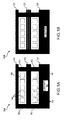
- FIGs. 1A-1B illustrate cross-sectional views of example structures of uncoupled magnetic core devices 100A and 100B having a 3-dimensional (3-D) helical coil and a 3-D magnetic-flux closed circuit in accordance with one or more implementations of the subject technology.
- the uncoupled magnetic core device (hereinafter "device") 100A includes a substrate 110, a first magnetic shell 120 formed on the substrate 110, and a first group of conductive (e.g., copper) traces 140 embedded in a first insulator layer 142 formed on the first magnetic shell 120.
- conductive e.g., copper
- the device 100A further includes a magnetic core plane 130 formed on the first insulator layer 142, a second group of conductive (e.g., copper) traces 144 embedded in a second insulator layer 146 formed on the magnetic core plane 130, and a second magnetic shell 122 formed on the second insulator layer 146.
- the substrate is formed of alumina ceramic (Al 2 O 3 ), silicon, glass, or similar materials, and the insulating layers 142 and 146 can be made, for example, of hard resist or other insulating materials.
- the first and second group of conductive traces 140 and 144 are horizontal parallel conductive traces, which are conductively coupled to one another, by using conductive vias, to form the 3-D helical coil that winds around the magnetic core plane 130.
- the cross-sectional area of the first and second group of conductive traces 140 and 144 can vary between 1x1 ⁇ m 2 , for low-current applications, and 10x10 ⁇ m 2 , for high-current applications.
- the subject technology allows formation of inductors as small as approximately 3x3x5 ⁇ m (height x width x length) formed ,for example, by 1x1 ⁇ m 2 conductors as a single-round coil, and as large as 65x65x500 ⁇ m formed ,for example, by 10x10 ⁇ m 2 conductors as a 5-rounds coil.
- the 3-D magnetic-flux closed circuit is formed by the first and second magnetic shells 120 and 122, the magnetic core plane 130, and vertical magnetic vias 150, which can be formed by, for example, ferric material such as Fe-Ni or Ni-Fe and Co-Fe, or other magnetic materials.
- the first and second magnetic shells 120 and 122 sandwich the conductor coils to minimize magnetic flux leakage and improve a Q factor of the inductor of device 100A.
- the magnetic vias complete the closed-loop magnetic flux interconnection between the magnetic core plane 130 and the first and second magnetic shells 120 and 122.
- the magnetic core plane 132 of the device 100B is laminated, for example, by forming the magnetic core plane 132 by multiple layers of magnetic material separated from one another by insulator layers (e.g., hard resist or other insulating materials).
- the magnetic core plane 132 includes a large number (e.g., >10) of laminated magnetic layers with thickness of the order of 0.1-0.2 ⁇ m.
- the laminated structure of the core plane 132 improves the device performance by reducing eddy current through the core plane 132, which can result in lower energy loss.
- the first and second magnetic shells 120 and 122 can also have laminated structures to further improve performance of the device 100B.
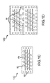
- FIGs. 1C-1D illustrate additional cross-sectional views 100C and 100D of the example structure of uncoupled magnetic core device 100A of FIG. 1A in accordance with one or more implementations of the subject technology.
- the cross section view 100C shown in FIG. 1C depicts the conductor (e.g., copper) vias 160 that couple the first group of conductive traces 140, which are seen as slanted lines, to the second group of conductive traces 144 (not seen in the cross-sectional view 100C).
- the magnetic vias 150 and insulator layers 170 are also seen in the cross-sectional view 100C.
- the magnetic core plane 130 of FIG. 1A can be further slotted into strips to reduce in-plane eddy current formation to reduce energy loss.
- the insulator layers 170 are used to fill the gaps formed between the strips of the magnetic core plane.
- the cross-sectional view 100D shows two similar 3-D magnetic core devices each enclosed in a separate closed magnetic flux circuit formed by magnetic vias 150.
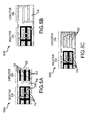
- FIGs. 2A through 2C illustrate cross-sectional views of example structures of a magnetic core device including coupled inductors in accordance with one or more implementations of the subject technology.
- the cross-sectional view 200A shows the magnetic core device with coupled inductors (e.g., 3-D helical coils) 210 and 220.
- the 3-D helical coil 210 is formed by the inter-coupling of conductive traces 212 and 214 through conductive vias 216 illustrated in FIG. 2C .
- the 3-D helical coil 220 is formed by the inter-coupling of conductive traces 242 and 244 through conductive vias 246 illustrated in FIG. 2C .
- the 3-D helical coils 210 and 220 are magnetically coupled via 3-D magnetic-flux closed circuits and respectively form the primary and secondary coils of a transformer.
- the number of turns of the primary and secondary coils 210 and 220 can be the same or different.
- the 3-D magnetic-flux closed circuits that magnetically couple the primary and secondary coils 210 and 220 include magnetic shells 220 and 222, magnetic core plate 230, and magnetic vias 250.
- the magnetic core plate 230 can be laminated and or slotted as described with respect to FIGs. 1B and 1C .
- the magnetic core plane 230 can include a large number (e.g., >10) of laminated magnetic layers with thickness of the order of 0.1-0.2 ⁇ m.
- the laminated structure of the core plane 230 can improve the device performance by reducing eddy current through the core plane 230, which can result in lower energy loss.
- the magnetic shells 220 and 222 can also have laminated structures to further improve performance of the magnetic core device of FIG. 2A .
- the primary and secondary coils 210 and 220 can be separated by the magnetic vias 252, which partition the 3-D magnetic-flux closed circuit into two different enclosed circuits.
- the implementation of the vias 252 is more clearly shown in the cross-sectional view 200C, which is similar to the cross-sectional view 100C of FIG. 1C , described above.
- FIG. 3 illustrates a cross-sectional view 300 of an example structure of hybrid coupled magnetic core devices having a 3-D helical coil and a 2-D spiral coil in accordance with one or more implementations of the subject technology.
- the magnetic core device with coupled inductors shown in the cross-sectional view 300 is similar to the magnetic core device shown in FIG. 2B , except that the first and second group of conductive traces 322 and 324 of the secondary coil 320 are formed in a same plane so that magnetic fields generated by the primary coil 310 and the secondary coil 320 are not parallel as in the case shown in FIG. 2B , but are substantially perpendicular to one another.
- This configuration of combining a 3-D helical coil 310 with a 2-D spiral coil 320 provides a difference in coupling characteristics, which can be useful in certain applications, where minimizing coupling is desirable.
- the coupling between the primary coil 310 and the secondary coil 320 can be adjusted, for example, by changing the thickness of the magnetic block 330 between the first and second group of conductive traces 322 and 324.
- the combination of the 3D helical coil 310 and the 2-D spiral coil 320 provides an opportunity for have a tunable magnetic coupling between the primary coil 310 and the secondary coil 320.
- FIGs. 4A-4B illustrate examples of inductor input/output (I/O) architectures 400A and 400B in accordance with one or more implementations of the subject technology.
- Implementation of the existing 2-D inductor devices limits input/output (I/O) contact pads and/or pins to be on the same surface of the inductor device.
- the subject technology advantageously allows the I/O contact pads and/or pins of the device be positioned on more than one surface of the device.
- the IO contact pads 410 and 412 are positioned on opposite surfaces of the inductor device.
- the I/O contact pads and/or pins can be placed on any or the entire multiple (e.g., 6) surfaces of the device.
- the IO contact pads 420, 430, and 440 are positioned on top, side, and bottom surfaces of the inductor device.
- the inductor device can be integrated in an interposer having a two-dimensional (2D) array of input/output (IO) connections, and the interposer can include a high-density die-to-die interconnection bus for coupling to a plurality of chips.
- FIGs. 5A through 5C illustrate examples of integrated inductor and capacitor filters in accordance with one or more implementations of the subject technology.
- one or more 3-D capacitors can be integrated with the one or more 3-D magnetic core device.
- the capacitor 520 is integrated with the 3-D inductor 510.
- the 3-D inductor 510 is formed by the conductors 514 and the magnetic core 512, as discussed above.
- a ceramic material 530 e.g., aluminum oxide
- the insulating material is used as the insulating material.
- the capacitor 520 is formed by conductive electrodes 524, connected to one another by conductive vias 526, and insulator layers formed by tantalum oxide layers 522 and the ceramic material 530. In one or more implementations, other insulator materials such as teflon can be used instead or in combination with the ceramic material. In some aspects, as shown in the cross-sectional view 500B of FIG. 5B , the capacitor 550 may be formed by using just one type of insulator, for example, the ceramic material 530. In some implementations, as shown in the cross-sectional view 500C of FIG. 5C , the capacitor 560 includes additional electrodes 580 formed by conductive layers in the same plane as the magnetic material layers 512.
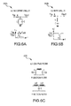
- FIGs. 6A through 6D illustrate examples of applications of a 3-D magnetic core device in accordance with one or more implementations of the subject technology.
- the integrated capacitor and the 3-D inductors can be coupled in parallel (e.g., as shown in FIG. 6A ) or in series (e.g., as shown in FIG. 6B ) or other configurations (e.g., as shown in FIG. 6C ) to achieve different known filter functions.
- integrated 3-D inductors and capacitors can be interconnected to form switching regulators (e.g., circuit 600D shown in in FIG. 6D ).
- switching regulators e.g., circuit 600D shown in in FIG. 6D
- the capacitors C1 at the input of the switching regulator circuit 600D or capacitors C2 and C3 connected to the outputs of the switching regulator circuit 600D can be integrated with inductors, as explained above.
- FIGs. 7A through 7E illustrate examples of integrated inductors and capacitors into a passive device package (PDP) in accordance with one or more implementations of the subject technology.
- the PDP 710 shown in FIG. 7A includes multiple magnetic core inductors of the subject technology integrated with one or more capacitors.
- the PDP 710 can be a ball grid array (BGA) or land grid array (LGA) surface mount PDP having an array of electrically conductive balls 712 on the bottom surface for interconnection to another PDP, an interposer, or an integrated circuit (IC) packaging substrate.
- the PDP 720, as shown in FIG. 7B has electrical interconnect contact terminals 722 on the top of the PDP forming an array of contact terminals 722 with a pattern matching the array of balls 712.
- the contact terminals 722 can be made of an electrically conductive material and can be of any shape, for example, circular, rectangular, square, hexagonal, etc.
- Multiple PDPs 720 can be coupled to one another by mounting on the top of one another as shown in FIG. 7C and interconnecting through the array of balls 712 and the array of contact terminals 722.
- a PDP 730 as shown in FIG. 7D has multiple electrically conductive interconnect pads 732 on one or more side walls. The interconnect pads 732 are useful for coupling two or more PDP 730 together, as shown in FIG. 7E .
- FIGs. 8A through 8E illustrate examples of apparatuses 800A through 800E using packaging integration of magnetic core inductors in accordance with one or more implementations of the subject technology.
- the apparatus 800A of FIG. 8A includes an IC packaging substrate 820 and an active chip 840 coupled to the IC packaging substrate 820 via an array of BGA or LGA formed of balls 846 that are electrically connected to contact terminals 848.
- the active chip 840 includes an active portion 842 that includes active and passive electronic circuitry such as analog and/or digital circuitry.
- the IC packaging substrate 820 includes a core 822 and multiple top re-distribution layers (RDLs) (e.g., metal layers) 824 and multiple bottom RDLs 826.
- RDLs top re-distribution layers
- a discrete magnetic core 830 is embedded in the core 822 of the IC packaging substrate 820.
- the discrete magnetic core 830 can be, for example, a traditionally used surface mounting magnetic core inductor.
- This integration technique can employ the same manufacturing flow used for integrating surface mount discrete capacitors in the core of an IC packaging substrate.
- the discrete magnetic core 830 can be coupled to the active chip 840 through vias 832 in the RDLs 824 and contact terminals 848.
- the apparatus 800B shown in FIG. 8B is similar to the apparatus 800A of FIG. 8A , except for the discrete magnetic core 830, which is replaced with a high-density magnetic core inductor 850, realized on a silicon substrate and embedded in the core 822 of the IC packaging substrate 820.
- the magnetic core inductor 850 include the magnetic core devices disclosed above, such as the magnetic core devices 100A, 100B, 200A, 200B, and 300 of FIGs. 1A, 1B , 2A, 2B , and 3 , respectively.
- the coupling of the discrete magnetic core 830 to the active chip 840 is similar to the coupling of the discrete magnetic core 850 to the active chip 840 in FIG. 8A .
- embedding of magnetic core material on a silicon substrate can be done using a cavity in that silicon substrate or in the RDLs on top of that silicon substrate. Due to the high density nature of the metallization on a Silicon substrate, large value inductors can be realized on such inductors for a given footprint and profile.
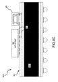
- the apparatus 800C shown in FIG. 8C is similar to the apparatus 800B of FIG. 8B , except that the magnetic core inductor 850 is not embedded in the core 822 of the IC packaging substrate 820, and instead is mounted on the IC packaging substrate 820.
- the magnetic core inductor 850 is mounted side-by-side with the active chip 840 on the top surface of the IC packaging substrate 820, and coupled to the active chip 840 through interconnections 815. Due to the low profile of the Silicon based magnetic core inductors 850, such integration is not expected to cause other issues such as height mismatch impacting heart-spreader or heat-sink mounting.
- the active chip 840 and the IC packaging substrate 820 are similar to those of the apparatus 800C of FIG. 8C , except that the active chip 840 includes vias 874 and contact terminals 876 that allow the magnetic core inductor 850, mounted on top of the active chip 840, be coupled to the active portion 842 of the active chip 840.
- the magnetic core inductor 850 is coupled to the contact terminals 876 through micro-bumps 852.
- the 3-D stacking shown in FIG. 8D provides a path of least amount of parasitics from the magnetic core inductor 850 to the active circuitry of the active chip 840.
- the active chip 840-land the IC packaging substrate 820 are similar to those of FIG. 8C .
- the high value inductor is realized on a silicon or glass interposer 880 that is inserted in between the active chip 840-1 and the IC packaging substrate 820.
- the magnetic core inductor 850 is inserted in the interposer 880 by creating a cavity in the interposer 880 or in the top or bottom RDLs of the interposer 880.
- the active chip 840-1 can be one of several active chips mounted on the interposer 880.
- the active chip 840-1 is coupled to the IC packaging substrate 820 through vias 882 passing through the interposer 880.
- the magnetic core inductor 850 inserted in the cavity of the interposer 880, the conductors that turn around that magnetic core inductor 850, include the top and bottom RDL turns and vias (e.g., 882) on the sides of the magnetic core inductor 850.
- the subject technology advantageously provides ways of increasing inductance density for a given surface area on the IC packaging substrate, by realizing the inductor around magnetic core material.
- the disclosed technology offers many advantages for applications such as voltage regulator output filtering, with devices having integrated on-chip voltage regulators. Such integration allows saving a multiple routing layers on the IC packaging substrate that are otherwise used for patterning the inductors.
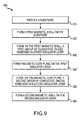
- FIG. 9 illustrates an example of a method 900 for providing a 3-D magnetic core device in accordance with one or more implementations of the subject technology.
- the blocks of the example method 900 are described herein as occurring in serial, or linearly. However, multiple blocks of the example method 900 can occur in parallel. In addition, the blocks of the example method 900 need not be performed in the order shown and/or one or more of the blocks of the example method 900 need not be performed.
- a substrate e.g., 110 of FIG. 1A
- a first magnetic shell e.g., 120 of FIG. 1A
- a first group of conductive traces e.g., 140 of FIG. 1A
- a first insulator layer e.g., 142 of FIG. 1A
- a magnetic core plane e.g., 130 of FIG. 1A
- a second group of conductive traces e.g., 144 of FIG. 1A
- embedded in a second insulator layer e.g., 146 of FIG. 1A
- a second magnetic shell e.g., 122 of FIG. 1A
- FIG. 10 illustrates an example of a wireless communication device employing features of the subject technology in accordance with one or more implementations of the subject technology.
- the wireless communication device 1000 includes a radio-frequency (RF) antenna 1010, a receiver 1020, a transmitter 1030, a baseband processing module 1040, a memory 1050, a processor 1060, a local oscillator generator (LOGEN) 1070, a power supply 1080 and a sensor module 1090.
- RF radio-frequency
- LOGEN local oscillator generator
- the blocks 1020- 1070 can be realized in a single chip or a single system on chip, or can be realized in a multi-chip chipset.
- the RF antenna 1010 can be suitable for transmitting and/or receiving RF signals (e.g., wireless signals) over a wide range of frequencies. Although a single RF antenna 1010 is illustrated, the subject technology is not so limited.
- the receiver 1020 comprises suitable logic circuitry and/or code that can be operable to receive and process signals from the RF antenna 1010.
- the receiver 1020 may, for example, be operable to amplify and/or down-convert received wireless signals.
- the receiver 1020 is operable to cancel noise in received signals and can be linear over a wide range of frequencies. In this manner, the receiver 1020 is suitable for receiving signals in accordance with a variety of wireless standards. Wi-Fi, WiMAX, Bluetooth, and various cellular standards.
- the transmitter 1030 comprises suitable logic circuitry and/or code that can be operable to process and transmit signals from the RF antenna 1010.
- the transmitter 1030 may, for example, be operable to up-convert baseband signals to RF signals and amplify RF signals.
- the transmitter 1030 is operable to up-convert and to amplify baseband signals processed in accordance with a variety of wireless standards. Examples of such standards include Wi-Fi, WiMAX, Bluetooth, and various cellular standards.
- the transmitter 1030 is operable to provide signals for further amplification by one or more power amplifiers.
- the duplexer 1012 provides isolation in the transmit band to avoid saturation of the receiver 1020 or damaging parts of the receiver 1020, and to relax one or more design requirements of the receiver 1020. Furthermore, the duplexer 1012 can attenuate the noise in the receive band.
- the duplexer is operable in multiple frequency bands of various wireless standards.
- the baseband processing module 1040 comprises suitable logic, circuitry, interfaces, and/or code that can be operable to perform processing of baseband signals.
- the baseband processing module 1040 may, for example, analyze received signals and generate control and/or feedback signals for configuring various components of the wireless communication device 1000 such as the receiver 1020.
- the baseband processing module 1040 is operable to encode, decode, transcode, modulate, demodulate, encrypt, decrypt, scramble, descramble, and/or otherwise process data in accordance with one or more wireless standards.
- the processor 1060 comprises suitable logic, circuitry, and/or code that can enable processing data and/or controlling operations of the wireless communication device 1000.
- the processor 1060 is enabled to provide control signals to various other portions of the wireless communication device 1000.
- the processor 1060 can also control transfers of data between various portions of the wireless communication device 1000.
- the processor 1060 can enable implementation of an operating system or otherwise execute code to manage operations of the wireless communication device 1000.
- the memory 1050 comprises suitable logic, circuitry, and/or code that can enable storage of various types of information such as received data, generated data, code, and/or configuration information.
- the memory 1050 includes, for example, RAM, ROM, flash, and/or magnetic storage.
- the memory 1050 may include a RAM, DRAM, SRAM, T-RAM, Z-RAM, TTRAM, or any other storage media.
- the local oscillator generator (LOGEN) 1070 comprises suitable logic, circuitry, interfaces, and/or code that can be operable to generate one or more oscillating signals of one or more frequencies.
- the LOGEN 1070 can be operable to generate digital and/or analog signals. In this manner, the LOGEN 1070 can be operable to generate one or more clock signals and/or sinusoidal signals. Characteristics of the oscillating signals such as the frequency and duty cycle can be determined based on one or more control signals from, for example, the processor 1060 and/or the baseband processing module 1040.
- the processor 1060 can configure the various components of the wireless communication device 1000 based on a wireless standard according to which it is desired to receive signals.
- Wireless signals can be received via the RF antenna 1010 and amplified and down-converted by the receiver 1020.
- the baseband processing module 1040 can perform noise estimation and/or noise cancellation, decoding, and/or demodulation of the baseband signals. In this manner, information in the received signal can be recovered and utilized appropriately.
- the information can be audio and/or video to be presented to a user of the wireless communication device, data to be stored to the memory 1050, and/or information affecting and/or enabling operation of the wireless communication device 1000.
- the baseband processing module 1040 can modulate, encode and perform other processing on audio, video, and/or control signals to be transmitted by the transmitter 1030 in accordance to various wireless standards.
- circuits of the wireless communication device 1000 for example, some modules and/or components of the receiver 1020 and transmitter 1030 can be implemented using the uncoupled (e.g., magnetic core devices of FIGs. 1A and 1B ) or coupled 3-D inductors (e.g., magnetic core devices of FIGs. 2A and 2B ) of the subject technology to form of various filters (e.g., filters of FIGs. 6A through 6C ).
- the power supply 1080 may, for example, use switching regulators that can be formed by interconnection integrated capacitors with the 3-D inductors of the subject technology (e.g., switching regulator of FIG. 6D ), as explained above.
- the phrase "at least one of” preceding a series of items, with the term “and” or “or” to separate any of the items, modifies the list as a whole, rather than each member of the list (i.e., each item).
- the phrase "at least one of” does not require selection of at least one of each item listed; rather, the phrase allows a meaning that includes at least one of any one of the items, and/or at least one of any combination of the items, and/or at least one of each of the items.
- phrases “at least one of A, B, and C” or “at least one of A, B, or C” each refer to only A, only B, or only C; any combination of A, B, and C; and/or at least one of each of A, B, and C.
- a phrase such as "an aspect” does not imply that such aspect is essential to the subject technology or that such aspect applies to all configurations of the subject technology.
- a disclosure relating to an aspect can apply to all configurations, or one or more configurations.
- An aspect can provide one or more examples of the disclosure.
- a phrase such as an "aspect” refers to one or more aspects and vice versa.
- a phrase such as an "embodiment” does not imply that such embodiment is essential to the subject technology or that such embodiment applies to all configurations of the subject technology.
- a disclosure relating to an embodiment can apply to all embodiments, or one or more embodiments.
- An embodiment can provide one or more examples of the disclosure.
- a phrase such an "embodiment” can refer to one or more embodiments and vice versa.
- a phrase such as a "configuration” does not imply that such configuration is essential to the subject technology or that such configuration applies to all configurations of the subject technology.
- a disclosure relating to a configuration can apply to all configurations, or one or more configurations.
- a configuration can provide one or more examples of the disclosure.
- a phrase such as a "configuration” can refer to one or more configurations and vice versa.
- a 3-dimensinal (3-D) magnetic core device includes a substrate, a first magnetic shell formed on the substrate, and a first group of conductive traces embedded in a first insulator layer formed on the first magnetic shell.
- a magnetic core plane is formed on the first insulator layer, and a second group of conductive traces are embedded in a second insulator layer formed on the magnetic core plane.
- a second magnetic shell is formed on the second insulator layer, and the first and second group of conductive traces are conductively coupled by using conductive vias.
Landscapes
- Engineering & Computer Science (AREA)
- Power Engineering (AREA)
- Microelectronics & Electronic Packaging (AREA)
- Manufacturing & Machinery (AREA)
- Coils Or Transformers For Communication (AREA)
Applications Claiming Priority (4)
| Application Number | Priority Date | Filing Date | Title |
|---|---|---|---|
| US201461980565P | 2014-04-16 | 2014-04-16 | |
| US201462062716P | 2014-10-10 | 2014-10-10 | |
| US201562114489P | 2015-02-10 | 2015-02-10 | |
| US14/684,256 US9693461B2 (en) | 2014-04-16 | 2015-04-10 | Magnetic-core three-dimensional (3D) inductors and packaging integration |
Publications (3)
| Publication Number | Publication Date |
|---|---|
| EP2940700A2 true EP2940700A2 (de) | 2015-11-04 |
| EP2940700A3 EP2940700A3 (de) | 2015-12-09 |
| EP2940700B1 EP2940700B1 (de) | 2020-06-10 |
Family
ID=52829030
Family Applications (1)
| Application Number | Title | Priority Date | Filing Date |
|---|---|---|---|
| EP15163694.1A Active EP2940700B1 (de) | 2014-04-16 | 2015-04-15 | Dreidimensionale (3d) magnetkerninduktoren und verpackungsintegration |
Country Status (4)
| Country | Link |
|---|---|
| US (1) | US9693461B2 (de) |
| EP (1) | EP2940700B1 (de) |
| CN (2) | CN105185554B (de) |
| HK (1) | HK1215616A1 (de) |
Families Citing this family (52)
| Publication number | Priority date | Publication date | Assignee | Title |
|---|---|---|---|---|
| US11116081B2 (en) | 2012-09-11 | 2021-09-07 | Ferric Inc. | Laminated magnetic core inductor with magnetic flux closure path parallel to easy axes of magnetization of magnetic layers |
| US11064610B2 (en) | 2012-09-11 | 2021-07-13 | Ferric Inc. | Laminated magnetic core inductor with insulating and interface layers |
| US11197374B2 (en) | 2012-09-11 | 2021-12-07 | Ferric Inc. | Integrated switched inductor power converter having first and second powertrain phases |
| US11058001B2 (en) * | 2012-09-11 | 2021-07-06 | Ferric Inc. | Integrated circuit with laminated magnetic core inductor and magnetic flux closure layer |
| US11302469B2 (en) | 2014-06-23 | 2022-04-12 | Ferric Inc. | Method for fabricating inductors with deposition-induced magnetically-anisotropic cores |
| US10103627B2 (en) * | 2015-02-26 | 2018-10-16 | Altera Corporation | Packaged integrated circuit including a switch-mode regulator and method of forming the same |
| US10470309B2 (en) * | 2015-09-20 | 2019-11-05 | Qualcomm Incorporated | Inductor and capacitor integrated on a substrate |
| US9865387B2 (en) | 2015-12-02 | 2018-01-09 | Intel IP Corporation | Electronic package with coil formed on core |
| CN107154301B (zh) * | 2016-03-03 | 2018-12-25 | 台达电子企业管理(上海)有限公司 | 磁性组件 |
| CN111952293B (zh) * | 2019-05-15 | 2022-07-01 | 台达电子企业管理(上海)有限公司 | 功率模块及其制造方法 |
| US12058814B2 (en) * | 2016-03-03 | 2024-08-06 | Delta Electronics (Shanghai) Co., Ltd. | Power module and manufacturing method thereof |
| US11277067B2 (en) | 2016-03-03 | 2022-03-15 | Delta Electronics, Inc. | Power module and manufacturing method thereof |
| JP6693228B2 (ja) * | 2016-03-30 | 2020-05-13 | Tdk株式会社 | 電子部品搭載基板 |
| CN106876379B (zh) * | 2016-07-07 | 2019-10-08 | 威盛电子股份有限公司 | 半导体装置 |
| JP6593274B2 (ja) * | 2016-08-03 | 2019-10-23 | 株式会社豊田自動織機 | 多層基板 |
| US10083922B2 (en) * | 2016-11-23 | 2018-09-25 | Intel Corporation | Inductor interconnect |
| US10403707B2 (en) * | 2017-03-31 | 2019-09-03 | Qualcomm Incorporated | Array type inductor |
| JP6766740B2 (ja) | 2017-04-20 | 2020-10-14 | 株式会社村田製作所 | プリント配線基板およびスイッチングレギュレータ |
| CN107564884B (zh) * | 2017-08-30 | 2019-08-30 | 华进半导体封装先导技术研发中心有限公司 | 集成磁芯电感的转接板及其制造方法 |
| US10910321B2 (en) | 2017-11-29 | 2021-02-02 | Taiwan Semiconductor Manufacturing Co., Ltd. | Semiconductor device and method of making the same |
| US10867740B2 (en) * | 2017-11-30 | 2020-12-15 | Qualcomm Incorporated | Inductor apparatus and method of fabricating |
| WO2019160880A1 (en) * | 2018-02-13 | 2019-08-22 | Cirrus Logic International Semiconductor Ltd. | Fabrication of integrated circuit including passive electrical component |
| US11527483B2 (en) * | 2018-06-29 | 2022-12-13 | Intel Corporation | Package including fully integrated voltage regulator circuitry within a substrate |
| US11348718B2 (en) * | 2018-06-29 | 2022-05-31 | Intel Corporation | Substrate embedded magnetic core inductors and method of making |
| US11357096B2 (en) | 2018-07-05 | 2022-06-07 | Intel Corporation | Package substrate inductor having thermal interconnect structures |
| US12336196B2 (en) * | 2018-08-21 | 2025-06-17 | Intel Corporation | Magnetic core inductors on package substrates |
| TWI698008B (zh) * | 2018-08-31 | 2020-07-01 | 英屬開曼群島商鳳凰先驅股份有限公司 | 具能量轉換功能之集積化驅動模組及其製造方法 |
| US11908605B2 (en) * | 2018-11-13 | 2024-02-20 | Sg Micro (Suzhou) Limited | Integrated magnetics with closed-loop flux path |
| WO2020123694A1 (en) * | 2018-12-14 | 2020-06-18 | Zglue Inc. | Method for creation of different designs by combining a set of pre-defined disjoint masks |
| CN111786541B (zh) | 2019-03-18 | 2021-10-29 | 台达电子工业股份有限公司 | 电压调节模块 |
| US11723222B2 (en) * | 2019-05-09 | 2023-08-08 | Microchip Technology Incorporated | Integrated circuit (IC) package with integrated inductor having core magnetic field (B field) extending parallel to substrate |
| US11837575B2 (en) * | 2019-08-26 | 2023-12-05 | Taiwan Semiconductor Manufacturing Company, Ltd. | Bonding passive devices on active device dies to form 3D packages |
| CN112731996B (zh) * | 2019-10-28 | 2022-07-15 | 台达电子工业股份有限公司 | 电压调节模块 |
| US11101228B1 (en) * | 2020-02-13 | 2021-08-24 | Qualcomm Incorporated | Integrated circuit package with a magnetic core |
| US11557421B2 (en) | 2020-03-05 | 2023-01-17 | Globalfoundries Dresden Module One Limited Liability Company & Co. Kg | Integrated circuit structure with dielectric material to cover horizontally separated metal layers, and related method |
| US11270986B2 (en) | 2020-05-18 | 2022-03-08 | Analog Devices, Inc. | Package with overhang inductor |
| KR102815728B1 (ko) | 2020-06-22 | 2025-06-02 | 삼성전자주식회사 | 반도체 패키지 |
| CN115803832B (zh) * | 2020-07-27 | 2026-01-09 | 华为技术有限公司 | 电感器件及电子设备 |
| CN114188311B (zh) * | 2020-09-15 | 2026-04-10 | 联华电子股份有限公司 | 半导体结构 |
| CN119813718A (zh) * | 2020-09-25 | 2025-04-11 | 台达电子工业股份有限公司 | 功率转换模块 |
| JP7628810B2 (ja) * | 2020-11-19 | 2025-02-12 | ローム株式会社 | 半導体発光装置 |
| US12322695B2 (en) | 2020-12-01 | 2025-06-03 | Ferric Inc. | Magnetic core with hard ferromagnetic biasing layers and structures containing same |
| KR20220087784A (ko) | 2020-12-18 | 2022-06-27 | 삼성전자주식회사 | 반도체 패키지 및 반도체 패키지의 제조 방법 |
| CN112992476B (zh) * | 2021-02-05 | 2022-08-12 | 合肥矽力杰半导体技术有限公司 | 变压器,以及封装模块 |
| CN113053849B (zh) * | 2021-03-04 | 2022-02-15 | 珠海越亚半导体股份有限公司 | 集成电感的嵌埋支撑框架、基板及其制作方法 |
| US12309929B2 (en) * | 2021-03-10 | 2025-05-20 | Monolithic Power Systems, Inc. | Sandwich structure power supply module |
| US11764171B2 (en) * | 2021-04-27 | 2023-09-19 | Taiwan Semiconductor Manufacturing Co., Ltd. | Integrated circuit structure and method |
| US20220375865A1 (en) * | 2021-05-18 | 2022-11-24 | Intel Corporation | Microelectronic assemblies with glass substrates and magnetic core inductors |
| US20230197644A1 (en) * | 2021-12-17 | 2023-06-22 | Intel Corporation | Semiconductor Package, Semiconductor Die and Method for Forming a Semiconductor Package or a Semiconductor Die |
| US12125713B2 (en) | 2022-03-22 | 2024-10-22 | Ferric Inc. | Method for manufacturing ferromagnetic-dielectric composite material |
| KR20250007722A (ko) * | 2023-07-06 | 2025-01-14 | 삼성전자주식회사 | 반도체 패키지 |
| US20250096089A1 (en) * | 2023-09-19 | 2025-03-20 | Advanced Micro Devices, Inc. | Chip package with embedded and shielded inductors |
Family Cites Families (10)
| Publication number | Priority date | Publication date | Assignee | Title |
|---|---|---|---|---|
| US5070317A (en) * | 1989-01-17 | 1991-12-03 | Bhagat Jayant K | Miniature inductor for integrated circuits and devices |
| US5576680A (en) * | 1994-03-01 | 1996-11-19 | Amer-Soi | Structure and fabrication process of inductors on semiconductor chip |
| US7140092B2 (en) | 2003-01-16 | 2006-11-28 | Georgia Tech Research Corporation | Methods for manufacturing inductor cores |
| JP2004296816A (ja) | 2003-03-27 | 2004-10-21 | Fuji Electric Device Technology Co Ltd | 磁気誘導素子およびそれを用いた超小型電力変換装置 |
| US20060267718A1 (en) * | 2005-05-25 | 2006-11-30 | Intel Corporation | Microelectronic inductor with high inductance magnetic core |
| US7791837B2 (en) | 2006-03-31 | 2010-09-07 | Tdk Corporation | Thin film device having thin film coil wound on magnetic film |
| JP2007273802A (ja) | 2006-03-31 | 2007-10-18 | Tdk Corp | 薄膜デバイス |
| JP4867698B2 (ja) | 2007-02-20 | 2012-02-01 | Tdk株式会社 | 薄膜磁気デバイス及びこれを有する電子部品モジュール |
| US8655272B2 (en) | 2009-07-07 | 2014-02-18 | Nokia Corporation | Wireless charging coil filtering |
| US8558344B2 (en) | 2011-09-06 | 2013-10-15 | Analog Devices, Inc. | Small size and fully integrated power converter with magnetics on chip |
-
2015
- 2015-04-10 US US14/684,256 patent/US9693461B2/en active Active
- 2015-04-15 EP EP15163694.1A patent/EP2940700B1/de active Active
- 2015-04-16 CN CN201510181884.XA patent/CN105185554B/zh active Active
- 2015-04-16 CN CN201520231363.6U patent/CN204927008U/zh not_active Expired - Fee Related
-
2016
- 2016-03-23 HK HK16103459.0A patent/HK1215616A1/zh unknown
Non-Patent Citations (1)
| Title |
|---|
| None |
Also Published As
| Publication number | Publication date |
|---|---|
| HK1215616A1 (zh) | 2016-09-02 |
| CN204927008U (zh) | 2015-12-30 |
| CN105185554B (zh) | 2018-01-19 |
| US9693461B2 (en) | 2017-06-27 |
| CN105185554A (zh) | 2015-12-23 |
| US20150302974A1 (en) | 2015-10-22 |
| EP2940700B1 (de) | 2020-06-10 |
| EP2940700A3 (de) | 2015-12-09 |
Similar Documents
| Publication | Publication Date | Title |
|---|---|---|
| US9693461B2 (en) | Magnetic-core three-dimensional (3D) inductors and packaging integration | |
| US20250294781A1 (en) | Magnetic core inductors on package substrates | |
| US10256286B2 (en) | Integrated inductor for integrated circuit devices | |
| US7280024B2 (en) | Integrated transformer structure and method of fabrication | |
| US8907448B2 (en) | Small size and fully integrated power converter with magnetics on chip | |
| US8564092B2 (en) | Power convertor device and construction methods | |
| US11532894B2 (en) | Antenna apparatus | |
| US10854986B2 (en) | Antenna apparatus | |
| US20190096828A1 (en) | Semiconductor package structure | |
| US20170092594A1 (en) | Low profile package with passive device | |
| US8093982B2 (en) | Three dimensional inductor and transformer design methodology of glass technology | |
| US11245201B2 (en) | Antenna apparatus | |
| US9064631B2 (en) | Through-chip interface (TCI) structure for wireless chip-to-chip communication | |
| US9888577B2 (en) | Passive electrical devices with a polymer carrier | |
| EP3345218B1 (de) | Integration von induktoren mit einem system-on-chip (soc) mit erweitertem knoten unter verwendung von glaswafern mit induktoren und verbindung von wafer zu wafer | |
| EP3120674B1 (de) | Integration eines nach oben gerichteten substrats mit lötkugelverbindung in einem halbleitergehäuse | |
| US7209026B2 (en) | Integrated package inductor for integrated circuit devices | |
| US20250218647A1 (en) | Multi-die transformer power modules | |
| US20230335511A1 (en) | Packaging Substrate | |
| WO2009057018A2 (en) | Rf-ic packaging method and circuits obtained thereby | |
| US20210151898A1 (en) | Antenna apparatus | |
| US12402332B2 (en) | Integrated passive devices |
Legal Events
| Date | Code | Title | Description |
|---|---|---|---|
| PUAI | Public reference made under article 153(3) epc to a published international application that has entered the european phase |
Free format text: ORIGINAL CODE: 0009012 |
|
| 17P | Request for examination filed |
Effective date: 20150415 |
|
| AK | Designated contracting states |
Kind code of ref document: A2 Designated state(s): AL AT BE BG CH CY CZ DE DK EE ES FI FR GB GR HR HU IE IS IT LI LT LU LV MC MK MT NL NO PL PT RO RS SE SI SK SM TR |
|
| AX | Request for extension of the european patent |
Extension state: BA ME |
|
| PUAL | Search report despatched |
Free format text: ORIGINAL CODE: 0009013 |
|
| AK | Designated contracting states |
Kind code of ref document: A3 Designated state(s): AL AT BE BG CH CY CZ DE DK EE ES FI FR GB GR HR HU IE IS IT LI LT LU LV MC MK MT NL NO PL PT RO RS SE SI SK SM TR |
|
| AX | Request for extension of the european patent |
Extension state: BA ME |
|
| RIC1 | Information provided on ipc code assigned before grant |
Ipc: H01F 17/00 20060101AFI20151030BHEP Ipc: H01F 27/28 20060101ALN20151030BHEP Ipc: H01F 41/04 20060101ALI20151030BHEP |
|
| RIN1 | Information on inventor provided before grant (corrected) |
Inventor name: KHAN, REZAUR RAHMAN Inventor name: KARIKALAN, SAMPATH KOMARAPALAYAM VELAYUDHAM Inventor name: VORENKAMP, PIETER |
|
| RAP1 | Party data changed (applicant data changed or rights of an application transferred) |
Owner name: AVAGO TECHNOLOGIES GENERAL IP (SINGAPORE) PTE. LTD |
|
| STAA | Information on the status of an ep patent application or granted ep patent |
Free format text: STATUS: EXAMINATION IS IN PROGRESS |
|
| 17Q | First examination report despatched |
Effective date: 20181106 |
|
| RAP1 | Party data changed (applicant data changed or rights of an application transferred) |
Owner name: AVAGO TECHNOLOGIES INTERNATIONAL SALES PTE. LIMITE |
|
| GRAP | Despatch of communication of intention to grant a patent |
Free format text: ORIGINAL CODE: EPIDOSNIGR1 |
|
| STAA | Information on the status of an ep patent application or granted ep patent |
Free format text: STATUS: GRANT OF PATENT IS INTENDED |
|
| RIC1 | Information provided on ipc code assigned before grant |
Ipc: H01F 27/28 20060101ALN20191105BHEP Ipc: H01F 41/04 20060101ALI20191105BHEP Ipc: H01F 17/00 20060101AFI20191105BHEP |
|
| INTG | Intention to grant announced |
Effective date: 20191127 |
|
| GRAS | Grant fee paid |
Free format text: ORIGINAL CODE: EPIDOSNIGR3 |
|
| GRAA | (expected) grant |
Free format text: ORIGINAL CODE: 0009210 |
|
| STAA | Information on the status of an ep patent application or granted ep patent |
Free format text: STATUS: THE PATENT HAS BEEN GRANTED |
|
| AK | Designated contracting states |
Kind code of ref document: B1 Designated state(s): AL AT BE BG CH CY CZ DE DK EE ES FI FR GB GR HR HU IE IS IT LI LT LU LV MC MK MT NL NO PL PT RO RS SE SI SK SM TR |
|
| REG | Reference to a national code |
Ref country code: GB Ref legal event code: FG4D |
|
| REG | Reference to a national code |
Ref country code: CH Ref legal event code: EP Ref country code: AT Ref legal event code: REF Ref document number: 1279841 Country of ref document: AT Kind code of ref document: T Effective date: 20200615 |
|
| REG | Reference to a national code |
Ref country code: DE Ref legal event code: R096 Ref document number: 602015054007 Country of ref document: DE |
|
| REG | Reference to a national code |
Ref country code: IE Ref legal event code: FG4D |
|
| REG | Reference to a national code |
Ref country code: LT Ref legal event code: MG4D |
|
| PG25 | Lapsed in a contracting state [announced via postgrant information from national office to epo] |
Ref country code: SE Free format text: LAPSE BECAUSE OF FAILURE TO SUBMIT A TRANSLATION OF THE DESCRIPTION OR TO PAY THE FEE WITHIN THE PRESCRIBED TIME-LIMIT Effective date: 20200610 Ref country code: NO Free format text: LAPSE BECAUSE OF FAILURE TO SUBMIT A TRANSLATION OF THE DESCRIPTION OR TO PAY THE FEE WITHIN THE PRESCRIBED TIME-LIMIT Effective date: 20200910 Ref country code: FI Free format text: LAPSE BECAUSE OF FAILURE TO SUBMIT A TRANSLATION OF THE DESCRIPTION OR TO PAY THE FEE WITHIN THE PRESCRIBED TIME-LIMIT Effective date: 20200610 Ref country code: GR Free format text: LAPSE BECAUSE OF FAILURE TO SUBMIT A TRANSLATION OF THE DESCRIPTION OR TO PAY THE FEE WITHIN THE PRESCRIBED TIME-LIMIT Effective date: 20200911 Ref country code: LT Free format text: LAPSE BECAUSE OF FAILURE TO SUBMIT A TRANSLATION OF THE DESCRIPTION OR TO PAY THE FEE WITHIN THE PRESCRIBED TIME-LIMIT Effective date: 20200610 |
|
| REG | Reference to a national code |
Ref country code: NL Ref legal event code: MP Effective date: 20200610 |
|
| PG25 | Lapsed in a contracting state [announced via postgrant information from national office to epo] |
Ref country code: LV Free format text: LAPSE BECAUSE OF FAILURE TO SUBMIT A TRANSLATION OF THE DESCRIPTION OR TO PAY THE FEE WITHIN THE PRESCRIBED TIME-LIMIT Effective date: 20200610 Ref country code: HR Free format text: LAPSE BECAUSE OF FAILURE TO SUBMIT A TRANSLATION OF THE DESCRIPTION OR TO PAY THE FEE WITHIN THE PRESCRIBED TIME-LIMIT Effective date: 20200610 Ref country code: RS Free format text: LAPSE BECAUSE OF FAILURE TO SUBMIT A TRANSLATION OF THE DESCRIPTION OR TO PAY THE FEE WITHIN THE PRESCRIBED TIME-LIMIT Effective date: 20200610 Ref country code: BG Free format text: LAPSE BECAUSE OF FAILURE TO SUBMIT A TRANSLATION OF THE DESCRIPTION OR TO PAY THE FEE WITHIN THE PRESCRIBED TIME-LIMIT Effective date: 20200910 |
|
| REG | Reference to a national code |
Ref country code: AT Ref legal event code: MK05 Ref document number: 1279841 Country of ref document: AT Kind code of ref document: T Effective date: 20200610 |
|
| PG25 | Lapsed in a contracting state [announced via postgrant information from national office to epo] |
Ref country code: NL Free format text: LAPSE BECAUSE OF FAILURE TO SUBMIT A TRANSLATION OF THE DESCRIPTION OR TO PAY THE FEE WITHIN THE PRESCRIBED TIME-LIMIT Effective date: 20200610 Ref country code: AL Free format text: LAPSE BECAUSE OF FAILURE TO SUBMIT A TRANSLATION OF THE DESCRIPTION OR TO PAY THE FEE WITHIN THE PRESCRIBED TIME-LIMIT Effective date: 20200610 |
|
| PG25 | Lapsed in a contracting state [announced via postgrant information from national office to epo] |
Ref country code: RO Free format text: LAPSE BECAUSE OF FAILURE TO SUBMIT A TRANSLATION OF THE DESCRIPTION OR TO PAY THE FEE WITHIN THE PRESCRIBED TIME-LIMIT Effective date: 20200610 Ref country code: CZ Free format text: LAPSE BECAUSE OF FAILURE TO SUBMIT A TRANSLATION OF THE DESCRIPTION OR TO PAY THE FEE WITHIN THE PRESCRIBED TIME-LIMIT Effective date: 20200610 Ref country code: IT Free format text: LAPSE BECAUSE OF FAILURE TO SUBMIT A TRANSLATION OF THE DESCRIPTION OR TO PAY THE FEE WITHIN THE PRESCRIBED TIME-LIMIT Effective date: 20200610 Ref country code: SM Free format text: LAPSE BECAUSE OF FAILURE TO SUBMIT A TRANSLATION OF THE DESCRIPTION OR TO PAY THE FEE WITHIN THE PRESCRIBED TIME-LIMIT Effective date: 20200610 Ref country code: AT Free format text: LAPSE BECAUSE OF FAILURE TO SUBMIT A TRANSLATION OF THE DESCRIPTION OR TO PAY THE FEE WITHIN THE PRESCRIBED TIME-LIMIT Effective date: 20200610 Ref country code: EE Free format text: LAPSE BECAUSE OF FAILURE TO SUBMIT A TRANSLATION OF THE DESCRIPTION OR TO PAY THE FEE WITHIN THE PRESCRIBED TIME-LIMIT Effective date: 20200610 Ref country code: PT Free format text: LAPSE BECAUSE OF FAILURE TO SUBMIT A TRANSLATION OF THE DESCRIPTION OR TO PAY THE FEE WITHIN THE PRESCRIBED TIME-LIMIT Effective date: 20201012 Ref country code: ES Free format text: LAPSE BECAUSE OF FAILURE TO SUBMIT A TRANSLATION OF THE DESCRIPTION OR TO PAY THE FEE WITHIN THE PRESCRIBED TIME-LIMIT Effective date: 20200610 |
|
| PG25 | Lapsed in a contracting state [announced via postgrant information from national office to epo] |
Ref country code: SK Free format text: LAPSE BECAUSE OF FAILURE TO SUBMIT A TRANSLATION OF THE DESCRIPTION OR TO PAY THE FEE WITHIN THE PRESCRIBED TIME-LIMIT Effective date: 20200610 Ref country code: PL Free format text: LAPSE BECAUSE OF FAILURE TO SUBMIT A TRANSLATION OF THE DESCRIPTION OR TO PAY THE FEE WITHIN THE PRESCRIBED TIME-LIMIT Effective date: 20200610 Ref country code: IS Free format text: LAPSE BECAUSE OF FAILURE TO SUBMIT A TRANSLATION OF THE DESCRIPTION OR TO PAY THE FEE WITHIN THE PRESCRIBED TIME-LIMIT Effective date: 20201010 |
|
| REG | Reference to a national code |
Ref country code: DE Ref legal event code: R097 Ref document number: 602015054007 Country of ref document: DE |
|
| PLBE | No opposition filed within time limit |
Free format text: ORIGINAL CODE: 0009261 |
|
| STAA | Information on the status of an ep patent application or granted ep patent |
Free format text: STATUS: NO OPPOSITION FILED WITHIN TIME LIMIT |
|
| PG25 | Lapsed in a contracting state [announced via postgrant information from national office to epo] |
Ref country code: DK Free format text: LAPSE BECAUSE OF FAILURE TO SUBMIT A TRANSLATION OF THE DESCRIPTION OR TO PAY THE FEE WITHIN THE PRESCRIBED TIME-LIMIT Effective date: 20200610 |
|
| 26N | No opposition filed |
Effective date: 20210311 |
|
| PG25 | Lapsed in a contracting state [announced via postgrant information from national office to epo] |
Ref country code: SI Free format text: LAPSE BECAUSE OF FAILURE TO SUBMIT A TRANSLATION OF THE DESCRIPTION OR TO PAY THE FEE WITHIN THE PRESCRIBED TIME-LIMIT Effective date: 20200610 |
|
| PG25 | Lapsed in a contracting state [announced via postgrant information from national office to epo] |
Ref country code: MC Free format text: LAPSE BECAUSE OF FAILURE TO SUBMIT A TRANSLATION OF THE DESCRIPTION OR TO PAY THE FEE WITHIN THE PRESCRIBED TIME-LIMIT Effective date: 20200610 |
|
| GBPC | Gb: european patent ceased through non-payment of renewal fee |
Effective date: 20210415 |
|
| PG25 | Lapsed in a contracting state [announced via postgrant information from national office to epo] |
Ref country code: LU Free format text: LAPSE BECAUSE OF NON-PAYMENT OF DUE FEES Effective date: 20210415 |
|
| REG | Reference to a national code |
Ref country code: BE Ref legal event code: MM Effective date: 20210430 |
|
| PG25 | Lapsed in a contracting state [announced via postgrant information from national office to epo] |
Ref country code: GB Free format text: LAPSE BECAUSE OF NON-PAYMENT OF DUE FEES Effective date: 20210415 Ref country code: FR Free format text: LAPSE BECAUSE OF NON-PAYMENT OF DUE FEES Effective date: 20210430 Ref country code: CH Free format text: LAPSE BECAUSE OF NON-PAYMENT OF DUE FEES Effective date: 20210430 Ref country code: LI Free format text: LAPSE BECAUSE OF NON-PAYMENT OF DUE FEES Effective date: 20210430 |
|
| PG25 | Lapsed in a contracting state [announced via postgrant information from national office to epo] |
Ref country code: IE Free format text: LAPSE BECAUSE OF NON-PAYMENT OF DUE FEES Effective date: 20210415 |
|
| PG25 | Lapsed in a contracting state [announced via postgrant information from national office to epo] |
Ref country code: IS Free format text: LAPSE BECAUSE OF FAILURE TO SUBMIT A TRANSLATION OF THE DESCRIPTION OR TO PAY THE FEE WITHIN THE PRESCRIBED TIME-LIMIT Effective date: 20201010 |
|
| PG25 | Lapsed in a contracting state [announced via postgrant information from national office to epo] |
Ref country code: BE Free format text: LAPSE BECAUSE OF NON-PAYMENT OF DUE FEES Effective date: 20210430 |
|
| PG25 | Lapsed in a contracting state [announced via postgrant information from national office to epo] |
Ref country code: HU Free format text: LAPSE BECAUSE OF FAILURE TO SUBMIT A TRANSLATION OF THE DESCRIPTION OR TO PAY THE FEE WITHIN THE PRESCRIBED TIME-LIMIT; INVALID AB INITIO Effective date: 20150415 |
|
| PG25 | Lapsed in a contracting state [announced via postgrant information from national office to epo] |
Ref country code: CY Free format text: LAPSE BECAUSE OF FAILURE TO SUBMIT A TRANSLATION OF THE DESCRIPTION OR TO PAY THE FEE WITHIN THE PRESCRIBED TIME-LIMIT Effective date: 20200610 |
|
| PG25 | Lapsed in a contracting state [announced via postgrant information from national office to epo] |
Ref country code: MK Free format text: LAPSE BECAUSE OF FAILURE TO SUBMIT A TRANSLATION OF THE DESCRIPTION OR TO PAY THE FEE WITHIN THE PRESCRIBED TIME-LIMIT Effective date: 20200610 |
|
| PG25 | Lapsed in a contracting state [announced via postgrant information from national office to epo] |
Ref country code: TR Free format text: LAPSE BECAUSE OF FAILURE TO SUBMIT A TRANSLATION OF THE DESCRIPTION OR TO PAY THE FEE WITHIN THE PRESCRIBED TIME-LIMIT Effective date: 20200610 |
|
| PG25 | Lapsed in a contracting state [announced via postgrant information from national office to epo] |
Ref country code: MT Free format text: LAPSE BECAUSE OF FAILURE TO SUBMIT A TRANSLATION OF THE DESCRIPTION OR TO PAY THE FEE WITHIN THE PRESCRIBED TIME-LIMIT Effective date: 20200610 |
|
| PGFP | Annual fee paid to national office [announced via postgrant information from national office to epo] |
Ref country code: DE Payment date: 20250410 Year of fee payment: 11 |