EP2940736A1 - Cellule solaire à couches minces à base de composé, et procédé de fabrication de celle-ci - Google Patents
Cellule solaire à couches minces à base de composé, et procédé de fabrication de celle-ci Download PDFInfo
- Publication number
- EP2940736A1 EP2940736A1 EP13866575.7A EP13866575A EP2940736A1 EP 2940736 A1 EP2940736 A1 EP 2940736A1 EP 13866575 A EP13866575 A EP 13866575A EP 2940736 A1 EP2940736 A1 EP 2940736A1
- Authority
- EP
- European Patent Office
- Prior art keywords
- layer
- metal substrate
- photovoltaic cell
- compound thin
- film photovoltaic
- Prior art date
- Legal status (The legal status is an assumption and is not a legal conclusion. Google has not performed a legal analysis and makes no representation as to the accuracy of the status listed.)
- Withdrawn
Links
- 150000001875 compounds Chemical class 0.000 title claims abstract description 118
- 239000010409 thin film Substances 0.000 title claims abstract description 73
- 238000004519 manufacturing process Methods 0.000 title claims abstract description 26
- 239000000758 substrate Substances 0.000 claims abstract description 161
- 229910052751 metal Inorganic materials 0.000 claims abstract description 122
- 239000002184 metal Substances 0.000 claims abstract description 122
- PNEYBMLMFCGWSK-UHFFFAOYSA-N aluminium oxide Inorganic materials [O-2].[O-2].[O-2].[Al+3].[Al+3] PNEYBMLMFCGWSK-UHFFFAOYSA-N 0.000 claims abstract description 92
- 230000031700 light absorption Effects 0.000 claims abstract description 47
- 229910052782 aluminium Inorganic materials 0.000 claims abstract description 31
- 239000004411 aluminium Substances 0.000 claims abstract description 30
- XAGFODPZIPBFFR-UHFFFAOYSA-N aluminium Chemical compound [Al] XAGFODPZIPBFFR-UHFFFAOYSA-N 0.000 claims abstract description 30
- 239000011651 chromium Substances 0.000 claims abstract description 30
- XEEYBQQBJWHFJM-UHFFFAOYSA-N Iron Chemical group [Fe] XEEYBQQBJWHFJM-UHFFFAOYSA-N 0.000 claims abstract description 18
- 238000000151 deposition Methods 0.000 claims abstract description 17
- VYZAMTAEIAYCRO-UHFFFAOYSA-N Chromium Chemical compound [Cr] VYZAMTAEIAYCRO-UHFFFAOYSA-N 0.000 claims abstract description 15
- 229910052804 chromium Inorganic materials 0.000 claims abstract description 15
- 239000000470 constituent Substances 0.000 claims abstract description 9
- 229910052742 iron Inorganic materials 0.000 claims abstract description 9
- 230000003647 oxidation Effects 0.000 claims abstract description 8
- 238000007254 oxidation reaction Methods 0.000 claims abstract description 8
- 239000011521 glass Substances 0.000 claims description 27
- 238000010438 heat treatment Methods 0.000 claims description 8
- 229910000859 α-Fe Inorganic materials 0.000 claims description 8
- 238000009751 slip forming Methods 0.000 claims description 2
- 239000010949 copper Substances 0.000 description 21
- 238000000034 method Methods 0.000 description 20
- 239000000463 material Substances 0.000 description 16
- 230000032798 delamination Effects 0.000 description 13
- 229910052733 gallium Inorganic materials 0.000 description 12
- GYHNNYVSQQEPJS-UHFFFAOYSA-N Gallium Chemical compound [Ga] GYHNNYVSQQEPJS-UHFFFAOYSA-N 0.000 description 11
- XLOMVQKBTHCTTD-UHFFFAOYSA-N Zinc monoxide Chemical compound [Zn]=O XLOMVQKBTHCTTD-UHFFFAOYSA-N 0.000 description 11
- HVMJUDPAXRRVQO-UHFFFAOYSA-N copper indium Chemical compound [Cu].[In] HVMJUDPAXRRVQO-UHFFFAOYSA-N 0.000 description 11
- 239000003513 alkali Substances 0.000 description 10
- 230000004888 barrier function Effects 0.000 description 10
- 229910052802 copper Inorganic materials 0.000 description 8
- RYGMFSIKBFXOCR-UHFFFAOYSA-N Copper Chemical compound [Cu] RYGMFSIKBFXOCR-UHFFFAOYSA-N 0.000 description 7
- 239000011669 selenium Substances 0.000 description 7
- 150000003346 selenoethers Chemical class 0.000 description 7
- 240000002329 Inga feuillei Species 0.000 description 6
- PXHVJJICTQNCMI-UHFFFAOYSA-N Nickel Chemical compound [Ni] PXHVJJICTQNCMI-UHFFFAOYSA-N 0.000 description 6
- BUGBHKTXTAQXES-UHFFFAOYSA-N Selenium Chemical compound [Se] BUGBHKTXTAQXES-UHFFFAOYSA-N 0.000 description 6
- 230000000694 effects Effects 0.000 description 6
- 229910052717 sulfur Inorganic materials 0.000 description 6
- 239000010408 film Substances 0.000 description 5
- 229910052738 indium Inorganic materials 0.000 description 5
- 239000004065 semiconductor Substances 0.000 description 5
- 239000011787 zinc oxide Substances 0.000 description 5
- RBORURQQJIQWBS-QVRNUERCSA-N (4ar,6r,7r,7as)-6-(6-amino-8-bromopurin-9-yl)-2-hydroxy-2-sulfanylidene-4a,6,7,7a-tetrahydro-4h-furo[3,2-d][1,3,2]dioxaphosphinin-7-ol Chemical compound C([C@H]1O2)OP(O)(=S)O[C@H]1[C@@H](O)[C@@H]2N1C(N=CN=C2N)=C2N=C1Br RBORURQQJIQWBS-QVRNUERCSA-N 0.000 description 4
- WGLPBDUCMAPZCE-UHFFFAOYSA-N Trioxochromium Chemical compound O=[Cr](=O)=O WGLPBDUCMAPZCE-UHFFFAOYSA-N 0.000 description 4
- 238000000231 atomic layer deposition Methods 0.000 description 4
- 229910000423 chromium oxide Inorganic materials 0.000 description 4
- APFVFJFRJDLVQX-UHFFFAOYSA-N indium atom Chemical compound [In] APFVFJFRJDLVQX-UHFFFAOYSA-N 0.000 description 4
- 229910052711 selenium Inorganic materials 0.000 description 4
- 239000011734 sodium Substances 0.000 description 4
- 238000004544 sputter deposition Methods 0.000 description 4
- RWSOTUBLDIXVET-UHFFFAOYSA-N Dihydrogen sulfide Chemical compound S RWSOTUBLDIXVET-UHFFFAOYSA-N 0.000 description 3
- 229910052581 Si3N4 Inorganic materials 0.000 description 3
- VYPSYNLAJGMNEJ-UHFFFAOYSA-N Silicium dioxide Chemical compound O=[Si]=O VYPSYNLAJGMNEJ-UHFFFAOYSA-N 0.000 description 3
- NINIDFKCEFEMDL-UHFFFAOYSA-N Sulfur Chemical compound [S] NINIDFKCEFEMDL-UHFFFAOYSA-N 0.000 description 3
- UCKMPCXJQFINFW-UHFFFAOYSA-N Sulphide Chemical compound [S-2] UCKMPCXJQFINFW-UHFFFAOYSA-N 0.000 description 3
- PDYXSJSAMVACOH-UHFFFAOYSA-N [Cu].[Zn].[Sn] Chemical compound [Cu].[Zn].[Sn] PDYXSJSAMVACOH-UHFFFAOYSA-N 0.000 description 3
- 230000006872 improvement Effects 0.000 description 3
- 238000002488 metal-organic chemical vapour deposition Methods 0.000 description 3
- 150000004767 nitrides Chemical class 0.000 description 3
- 229910052760 oxygen Inorganic materials 0.000 description 3
- 230000008569 process Effects 0.000 description 3
- 239000011593 sulfur Substances 0.000 description 3
- 230000003746 surface roughness Effects 0.000 description 3
- XOLBLPGZBRYERU-UHFFFAOYSA-N tin dioxide Chemical compound O=[Sn]=O XOLBLPGZBRYERU-UHFFFAOYSA-N 0.000 description 3
- WUPHOULIZUERAE-UHFFFAOYSA-N 3-(oxolan-2-yl)propanoic acid Chemical compound OC(=O)CCC1CCCO1 WUPHOULIZUERAE-UHFFFAOYSA-N 0.000 description 2
- IJGRMHOSHXDMSA-UHFFFAOYSA-N Atomic nitrogen Chemical compound N#N IJGRMHOSHXDMSA-UHFFFAOYSA-N 0.000 description 2
- DGAQECJNVWCQMB-PUAWFVPOSA-M Ilexoside XXIX Chemical compound C[C@@H]1CC[C@@]2(CC[C@@]3(C(=CC[C@H]4[C@]3(CC[C@@H]5[C@@]4(CC[C@@H](C5(C)C)OS(=O)(=O)[O-])C)C)[C@@H]2[C@]1(C)O)C)C(=O)O[C@H]6[C@@H]([C@H]([C@@H]([C@H](O6)CO)O)O)O.[Na+] DGAQECJNVWCQMB-PUAWFVPOSA-M 0.000 description 2
- CPLXHLVBOLITMK-UHFFFAOYSA-N Magnesium oxide Chemical compound [Mg]=O CPLXHLVBOLITMK-UHFFFAOYSA-N 0.000 description 2
- ZLMJMSJWJFRBEC-UHFFFAOYSA-N Potassium Chemical compound [K] ZLMJMSJWJFRBEC-UHFFFAOYSA-N 0.000 description 2
- XUIMIQQOPSSXEZ-UHFFFAOYSA-N Silicon Chemical compound [Si] XUIMIQQOPSSXEZ-UHFFFAOYSA-N 0.000 description 2
- ATJFFYVFTNAWJD-UHFFFAOYSA-N Tin Chemical compound [Sn] ATJFFYVFTNAWJD-UHFFFAOYSA-N 0.000 description 2
- 239000005083 Zinc sulfide Substances 0.000 description 2
- MCMNRKCIXSYSNV-UHFFFAOYSA-N Zirconium dioxide Chemical compound O=[Zr]=O MCMNRKCIXSYSNV-UHFFFAOYSA-N 0.000 description 2
- 229910052783 alkali metal Inorganic materials 0.000 description 2
- 150000001340 alkali metals Chemical class 0.000 description 2
- 230000008901 benefit Effects 0.000 description 2
- 229910052980 cadmium sulfide Inorganic materials 0.000 description 2
- 229910052798 chalcogen Inorganic materials 0.000 description 2
- 150000001787 chalcogens Chemical class 0.000 description 2
- 238000006243 chemical reaction Methods 0.000 description 2
- 238000000224 chemical solution deposition Methods 0.000 description 2
- 230000000052 comparative effect Effects 0.000 description 2
- CDZGJSREWGPJMG-UHFFFAOYSA-N copper gallium Chemical compound [Cu].[Ga] CDZGJSREWGPJMG-UHFFFAOYSA-N 0.000 description 2
- 230000007797 corrosion Effects 0.000 description 2
- 238000005260 corrosion Methods 0.000 description 2
- 238000001704 evaporation Methods 0.000 description 2
- 229910003437 indium oxide Inorganic materials 0.000 description 2
- PJXISJQVUVHSOJ-UHFFFAOYSA-N indium(iii) oxide Chemical compound [O-2].[O-2].[O-2].[In+3].[In+3] PJXISJQVUVHSOJ-UHFFFAOYSA-N 0.000 description 2
- 238000001755 magnetron sputter deposition Methods 0.000 description 2
- 229910052759 nickel Inorganic materials 0.000 description 2
- 239000003921 oil Substances 0.000 description 2
- 229910052700 potassium Inorganic materials 0.000 description 2
- 239000011591 potassium Substances 0.000 description 2
- 238000007650 screen-printing Methods 0.000 description 2
- 239000010703 silicon Substances 0.000 description 2
- 229910052710 silicon Inorganic materials 0.000 description 2
- HQVNEWCFYHHQES-UHFFFAOYSA-N silicon nitride Chemical compound N12[Si]34N5[Si]62N3[Si]51N64 HQVNEWCFYHHQES-UHFFFAOYSA-N 0.000 description 2
- 229910052708 sodium Inorganic materials 0.000 description 2
- 239000010935 stainless steel Substances 0.000 description 2
- 229910001220 stainless steel Inorganic materials 0.000 description 2
- JBQYATWDVHIOAR-UHFFFAOYSA-N tellanylidenegermanium Chemical compound [Te]=[Ge] JBQYATWDVHIOAR-UHFFFAOYSA-N 0.000 description 2
- 239000010936 titanium Substances 0.000 description 2
- 229910052984 zinc sulfide Inorganic materials 0.000 description 2
- 229910000851 Alloy steel Inorganic materials 0.000 description 1
- 229910011255 B2O3 Inorganic materials 0.000 description 1
- ZOXJGFHDIHLPTG-UHFFFAOYSA-N Boron Chemical compound [B] ZOXJGFHDIHLPTG-UHFFFAOYSA-N 0.000 description 1
- 229910004613 CdTe Inorganic materials 0.000 description 1
- 229910002475 Cu2ZnSnS4 Inorganic materials 0.000 description 1
- 229910018038 Cu2ZnSnSe4 Inorganic materials 0.000 description 1
- ZOKXTWBITQBERF-UHFFFAOYSA-N Molybdenum Chemical compound [Mo] ZOKXTWBITQBERF-UHFFFAOYSA-N 0.000 description 1
- RTAQQCXQSZGOHL-UHFFFAOYSA-N Titanium Chemical compound [Ti] RTAQQCXQSZGOHL-UHFFFAOYSA-N 0.000 description 1
- QVGXLLKOCUKJST-UHFFFAOYSA-N atomic oxygen Chemical compound [O] QVGXLLKOCUKJST-UHFFFAOYSA-N 0.000 description 1
- QVQLCTNNEUAWMS-UHFFFAOYSA-N barium oxide Inorganic materials [Ba]=O QVQLCTNNEUAWMS-UHFFFAOYSA-N 0.000 description 1
- 239000002585 base Substances 0.000 description 1
- 229910052796 boron Inorganic materials 0.000 description 1
- 229910052793 cadmium Inorganic materials 0.000 description 1
- BDOSMKKIYDKNTQ-UHFFFAOYSA-N cadmium atom Chemical compound [Cd] BDOSMKKIYDKNTQ-UHFFFAOYSA-N 0.000 description 1
- ODINCKMPIJJUCX-UHFFFAOYSA-N calcium oxide Inorganic materials [Ca]=O ODINCKMPIJJUCX-UHFFFAOYSA-N 0.000 description 1
- 229910052799 carbon Inorganic materials 0.000 description 1
- 238000005229 chemical vapour deposition Methods 0.000 description 1
- 239000004020 conductor Substances 0.000 description 1
- 238000007796 conventional method Methods 0.000 description 1
- 229910052593 corundum Inorganic materials 0.000 description 1
- 230000007547 defect Effects 0.000 description 1
- 230000006866 deterioration Effects 0.000 description 1
- 239000002019 doping agent Substances 0.000 description 1
- 238000001035 drying Methods 0.000 description 1
- 238000005566 electron beam evaporation Methods 0.000 description 1
- 238000005265 energy consumption Methods 0.000 description 1
- 239000000446 fuel Substances 0.000 description 1
- 239000005431 greenhouse gas Substances 0.000 description 1
- 150000002472 indium compounds Chemical class 0.000 description 1
- 238000002844 melting Methods 0.000 description 1
- 238000012986 modification Methods 0.000 description 1
- 230000004048 modification Effects 0.000 description 1
- 229910052750 molybdenum Inorganic materials 0.000 description 1
- 239000011733 molybdenum Substances 0.000 description 1
- 229910052757 nitrogen Inorganic materials 0.000 description 1
- 239000003960 organic solvent Substances 0.000 description 1
- 239000001301 oxygen Substances 0.000 description 1
- 238000005268 plasma chemical vapour deposition Methods 0.000 description 1
- 238000010248 power generation Methods 0.000 description 1
- 239000002243 precursor Substances 0.000 description 1
- 238000005546 reactive sputtering Methods 0.000 description 1
- 239000011347 resin Substances 0.000 description 1
- 229920005989 resin Polymers 0.000 description 1
- 230000000717 retained effect Effects 0.000 description 1
- 229910052814 silicon oxide Inorganic materials 0.000 description 1
- 229910052709 silver Inorganic materials 0.000 description 1
- 229910000679 solder Inorganic materials 0.000 description 1
- 239000007921 spray Substances 0.000 description 1
- 238000005507 spraying Methods 0.000 description 1
- IATRAKWUXMZMIY-UHFFFAOYSA-N strontium oxide Inorganic materials [O-2].[Sr+2] IATRAKWUXMZMIY-UHFFFAOYSA-N 0.000 description 1
- 238000005092 sublimation method Methods 0.000 description 1
- GKCNVZWZCYIBPR-UHFFFAOYSA-N sulfanylideneindium Chemical compound [In]=S GKCNVZWZCYIBPR-UHFFFAOYSA-N 0.000 description 1
- 229910052714 tellurium Inorganic materials 0.000 description 1
- PORWMNRCUJJQNO-UHFFFAOYSA-N tellurium atom Chemical compound [Te] PORWMNRCUJJQNO-UHFFFAOYSA-N 0.000 description 1
- 229910001887 tin oxide Inorganic materials 0.000 description 1
- 229910052719 titanium Inorganic materials 0.000 description 1
- WFKWXMTUELFFGS-UHFFFAOYSA-N tungsten Chemical compound [W] WFKWXMTUELFFGS-UHFFFAOYSA-N 0.000 description 1
- 229910052721 tungsten Inorganic materials 0.000 description 1
- 239000010937 tungsten Substances 0.000 description 1
- 229910001845 yogo sapphire Inorganic materials 0.000 description 1
- 239000011701 zinc Substances 0.000 description 1
- 150000003752 zinc compounds Chemical class 0.000 description 1
- DRDVZXDWVBGGMH-UHFFFAOYSA-N zinc;sulfide Chemical compound [S-2].[Zn+2] DRDVZXDWVBGGMH-UHFFFAOYSA-N 0.000 description 1
Images

Classifications
-
- H—ELECTRICITY
- H10—SEMICONDUCTOR DEVICES; ELECTRIC SOLID-STATE DEVICES NOT OTHERWISE PROVIDED FOR
- H10F—INORGANIC SEMICONDUCTOR DEVICES SENSITIVE TO INFRARED RADIATION, LIGHT, ELECTROMAGNETIC RADIATION OF SHORTER WAVELENGTH OR CORPUSCULAR RADIATION
- H10F10/00—Individual photovoltaic cells, e.g. solar cells
- H10F10/10—Individual photovoltaic cells, e.g. solar cells having potential barriers
- H10F10/16—Photovoltaic cells having only PN heterojunction potential barriers
- H10F10/167—Photovoltaic cells having only PN heterojunction potential barriers comprising Group I-III-VI materials, e.g. CdS/CuInSe2 [CIS] heterojunction photovoltaic cells
-
- H—ELECTRICITY
- H10—SEMICONDUCTOR DEVICES; ELECTRIC SOLID-STATE DEVICES NOT OTHERWISE PROVIDED FOR
- H10F—INORGANIC SEMICONDUCTOR DEVICES SENSITIVE TO INFRARED RADIATION, LIGHT, ELECTROMAGNETIC RADIATION OF SHORTER WAVELENGTH OR CORPUSCULAR RADIATION
- H10F19/00—Integrated devices, or assemblies of multiple devices, comprising at least one photovoltaic cell covered by group H10F10/00, e.g. photovoltaic modules
- H10F19/30—Integrated devices, or assemblies of multiple devices, comprising at least one photovoltaic cell covered by group H10F10/00, e.g. photovoltaic modules comprising thin-film photovoltaic cells
-
- H—ELECTRICITY
- H10—SEMICONDUCTOR DEVICES; ELECTRIC SOLID-STATE DEVICES NOT OTHERWISE PROVIDED FOR
- H10F—INORGANIC SEMICONDUCTOR DEVICES SENSITIVE TO INFRARED RADIATION, LIGHT, ELECTROMAGNETIC RADIATION OF SHORTER WAVELENGTH OR CORPUSCULAR RADIATION
- H10F71/00—Manufacture or treatment of devices covered by this subclass
-
- H—ELECTRICITY
- H10—SEMICONDUCTOR DEVICES; ELECTRIC SOLID-STATE DEVICES NOT OTHERWISE PROVIDED FOR
- H10F—INORGANIC SEMICONDUCTOR DEVICES SENSITIVE TO INFRARED RADIATION, LIGHT, ELECTROMAGNETIC RADIATION OF SHORTER WAVELENGTH OR CORPUSCULAR RADIATION
- H10F77/00—Constructional details of devices covered by this subclass
- H10F77/10—Semiconductor bodies
- H10F77/12—Active materials
- H10F77/128—Active materials comprising only Group I-II-IV-VI kesterite materials, e.g. Cu2ZnSnSe4 or Cu2ZnSnS4
-
- H—ELECTRICITY
- H10—SEMICONDUCTOR DEVICES; ELECTRIC SOLID-STATE DEVICES NOT OTHERWISE PROVIDED FOR
- H10F—INORGANIC SEMICONDUCTOR DEVICES SENSITIVE TO INFRARED RADIATION, LIGHT, ELECTROMAGNETIC RADIATION OF SHORTER WAVELENGTH OR CORPUSCULAR RADIATION
- H10F77/00—Constructional details of devices covered by this subclass
- H10F77/10—Semiconductor bodies
- H10F77/16—Material structures, e.g. crystalline structures, film structures or crystal plane orientations
- H10F77/169—Thin semiconductor films on metallic or insulating substrates
- H10F77/1694—Thin semiconductor films on metallic or insulating substrates the films including Group I-III-VI materials, e.g. CIS or CIGS
-
- H—ELECTRICITY
- H10—SEMICONDUCTOR DEVICES; ELECTRIC SOLID-STATE DEVICES NOT OTHERWISE PROVIDED FOR
- H10F—INORGANIC SEMICONDUCTOR DEVICES SENSITIVE TO INFRARED RADIATION, LIGHT, ELECTROMAGNETIC RADIATION OF SHORTER WAVELENGTH OR CORPUSCULAR RADIATION
- H10F77/00—Constructional details of devices covered by this subclass
- H10F77/10—Semiconductor bodies
- H10F77/16—Material structures, e.g. crystalline structures, film structures or crystal plane orientations
- H10F77/169—Thin semiconductor films on metallic or insulating substrates
- H10F77/1698—Thin semiconductor films on metallic or insulating substrates the metallic or insulating substrates being flexible
- H10F77/1699—Thin semiconductor films on metallic or insulating substrates the metallic or insulating substrates being flexible the films including Group I-III-VI materials, e.g. CIS or CIGS on metal foils or polymer foils
-
- Y—GENERAL TAGGING OF NEW TECHNOLOGICAL DEVELOPMENTS; GENERAL TAGGING OF CROSS-SECTIONAL TECHNOLOGIES SPANNING OVER SEVERAL SECTIONS OF THE IPC; TECHNICAL SUBJECTS COVERED BY FORMER USPC CROSS-REFERENCE ART COLLECTIONS [XRACs] AND DIGESTS
- Y02—TECHNOLOGIES OR APPLICATIONS FOR MITIGATION OR ADAPTATION AGAINST CLIMATE CHANGE
- Y02E—REDUCTION OF GREENHOUSE GAS [GHG] EMISSIONS, RELATED TO ENERGY GENERATION, TRANSMISSION OR DISTRIBUTION
- Y02E10/00—Energy generation through renewable energy sources
- Y02E10/50—Photovoltaic [PV] energy
- Y02E10/541—CuInSe2 material PV cells
-
- Y—GENERAL TAGGING OF NEW TECHNOLOGICAL DEVELOPMENTS; GENERAL TAGGING OF CROSS-SECTIONAL TECHNOLOGIES SPANNING OVER SEVERAL SECTIONS OF THE IPC; TECHNICAL SUBJECTS COVERED BY FORMER USPC CROSS-REFERENCE ART COLLECTIONS [XRACs] AND DIGESTS
- Y02—TECHNOLOGIES OR APPLICATIONS FOR MITIGATION OR ADAPTATION AGAINST CLIMATE CHANGE
- Y02P—CLIMATE CHANGE MITIGATION TECHNOLOGIES IN THE PRODUCTION OR PROCESSING OF GOODS
- Y02P70/00—Climate change mitigation technologies in the production process for final industrial or consumer products
- Y02P70/50—Manufacturing or production processes characterised by the final manufactured product
Definitions
- the present invention relates to a compound thin-film photovoltaic cell and a method of manufacturing thereof.
- a compound thin-film photovoltaic cell in which an inorganic insulating layer and a compound light absorption layer such as a CIS-based thin-film or the like are stacked on a metal substrate such as a stainless substrate or the like.
- a thin insulating layer composed of oxide (SiOx or the like), nitride (Si 3 N 4 ) or the like is used as the inorganic insulating layer, for example.
- a stainless substrate in which aluminium is added is used as a metal substrate and a thin insulating layer or the like composed of alumina obtained by performing thermal oxidation on the stainless substrate and formed at its surface is used (see Patent Document 1, for example).
- Patent Document 1 Japanese Laid-open Patent Publication No. S63-155681
- the metal substrate when used, it is preferable to deposit a thick glass insulating layer using glass frit or the like on the metal substrate.
- a large advantage can be obtained by removing the influence of the oil pits or the scratches due to the thickness of the layer.
- the glass insulating layer when used, delamination at an interface between the upper surface of the metal substrate, which is a lower layer, and the glass insulating layer deposited on the metal substrate becomes a problem.
- the delamination causes deterioration of device characteristic of the compound thin-film photovoltaic cell.
- the delamination occurs due to the surface condition of the metal substrate, and the stress between the metal substrate and the glass insulating layer. Further, there is a possibility that the delamination occurs not only when manufacturing the compound thin-film photovoltaic cell, but also when the photovoltaic cell is being operated thereafter. Further, the degree of occurrence of the delamination 1 is high for the metal substrate whose surface roughness is small.
- the present invention is made in light of the above problems, and provides a compound thin-film photovoltaic cell and a method of manufacturing thereof capable of suppressing delamination between a metal substrate and an insulating layer.
- a method of manufacturing a compound thin-film photovoltaic cell including: preparing a metal substrate, whose main constituent is iron, containing aluminium (Al) and chromium (Cr), and forming an alumina layer at least on an element forming surface of the metal substrate by thermal oxidation; forming an insulating layer on the alumina layer; depositing a first electrode layer on the insulating layer; depositing a compound light absorption layer on the first electrode layer; and depositing a second electrode layer on the compound light absorption layer.
- a compound thin-film photovoltaic cell including: a metal substrate, whose main constituent is iron, containing aluminium (Al) and chromium (Cr); an alumina layer formed at least on an element forming surface of the metal substrate by thermal oxidation; an insulating layer formed on the alumina layer; a first electrode layer deposited on the insulating layer; a compound light absorption layer deposited on the first electrode layer; and a second electrode layer deposited on the compound light absorption layer.
- a compound thin-film photovoltaic cell and a method of manufacturing thereof capable of suppressing delamination between a metal substrate and an insulating layer can be provided.
- a CIS-based compound thin-film photovoltaic cell is exemplified in the following embodiment or the like, the present invention is applicable to a compound thin-film photovoltaic cell other than the CIS-based one.
- a CZTS-based compound thin-film photovoltaic cell may be used in which a light absorption layer is composed of a compound including copper (Cu), zinc (Zn), tin (Sn) and a chalcogen element (selenium (Se) or sulfur (S)).
- a CdTe-based compound thin-film photovoltaic cell or the like may be used in which a light absorption layer is composed of a compound including cadmium (Cd) and tellurium (Te) .
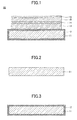
- Fig. 1 is a cross-sectional view illustrating an example of the CIS-based compound thin-film photovoltaic cell of the embodiment.
- a compound thin-film photovoltaic cell 10 includes a metal substrate 11 including an alumina layer 12 at its surface, an insulating layer 13, a first electrode layer 14, a compound light absorption layer 15 and a second electrode layer 16, in which the insulating layer 13, the first electrode layer 14, the compound light absorption layer 15 and the second electrode layer 16 are stacked on the alumina layer 12 of the metal substrate 11 in this order.
- each component that composes the compound thin-film photovoltaic cell 10 is explained.
- a surface at a light receiving side may be referred to as an "upper surface”, a surface opposite to this may be referred to as a “lower surface”, and a surface connecting the upper surface and the lower surface may be referred to as an "end surface”.
- the entirety of the upper surface, the lower surface and the end surfaces may be referred to as an "entire surface”.
- the upper surface of the metal substrate 11 may be particularly referred to as an "element forming surface”
- the lower surface of the metal substrate 11 may be particularly referred to as a "back surface”.
- the metal substrate 11 is a portion that becomes a base body on which the insulating layer 13, the first electrode layer 14, the compound light absorption layer 15 and the second electrode layer 16 are formed.
- the metal substrate 11 is a substrate whose main constituent is iron and containing aluminium (Al) and chromium (Cr).
- the entire surface of the metal substrate 11 is covered by the alumina layer 12 that is formed by thermal oxidation.
- the thickness of the metal substrate 11 may be about 0.2 mm to 0.6 mm, for example.
- the content of aluminium (Al) in the metal substrate 11 is greater than or equal to 0.5 weight % and less than or equal to 6.0 weight %.
- the content of aluminium (Al) in the metal substrate 11 is less than 0.5 weight %, it is not preferable because the alumina layer 12 is not sufficiently formed. Further, when the content of aluminium (Al) of the metal substrate 11 exceeds 6.0 weight %, it is not preferable because the coefficient of thermal expansion of the metal substrate 11 becomes large.
- a stainless substrate containing aluminium (Al) may be used as an example of the metal substrate 11. It is particularly preferable to use a ferrite-based stainless substrate containing aluminium (Al) as the metal substrate 11. This is because the delamination of the compound light absorption layer at the heat treatment or after the heat treatment can be prevented as the coefficient of thermal expansion of the ferrite-based stainless substrate is close to that of the CIS-based compound light absorption layer.
- the stainless substrate is a substrate made of stainless steel.
- the stainless steel means chromium (Cr) or alloy steel containing chromium (Cr) and nickel (Ni), in which the content of chromium (Cr) is greater than or equal to 10.5%.
- the metal substrate 11 is not limited to the stainless substrate containing aluminium (Al), and a substrate whose main constituent is iron and containing aluminium (Al) and less than 10.5% of chromium (Cr) may be used, for example.
- the substrate may further include nickel (Ni).
- the substrate whose main constituent is iron and containing aluminium (Al) and chromium (Cr) may include various stainless substrates including a ferrite-based stainless substrate and a substrate containing a kind of metal same as the stainless substrate in which the content of chromium (Cr) is less than 10.5%.
- chromium (Cr) is included at least about 8%.
- the metal substrate 11 may include silicon (Si).
- the alumina layer 12 covers the entire surface of the metal substrate 11.
- the alumina layer 12 is a layer formed such that aluminium (Al) contained in the metal substrate 11 is diffused at the entire surface of the metal substrate 11 under a predetermined condition.
- the thickness of the alumina layer 12 is greater than or equal to 30 nm.
- the thickness of the alumina layer 12 may be about 1 ⁇ m for a case that withstand voltage is to be improved between the metal substrate 11 and the first electrode layer 14 by a two-layered structure in which the alumina layer 12 and the insulating layer 13 are stacked.
- the alumina layer 12 is formed at least on the upper surface (element forming surface) of the metal substrate 11. Because the adhesion of the alumina layer 12 formed on the upper surface of the metal substrate 11 and the insulating layer 13 formed right above the alumina layer 12 can be improved.
- the insulating layer 13 is formed on the alumina layer 12 that is formed on the upper surface of the metal substrate 11.
- a glass As the material of the insulating layer 13, it is preferable to use a glass.
- a glass or a low-melting glass may be used whose component is at least one selected from silica (SiO 2 ), CaO, B 2 O 3 , SrO, BaO, Al 2 O 3 , ZnO, ZrO 2 and MgO.
- the reason why the glass is preferably used as the material of the insulating layer 13 is as follows. If organic resin is used as the material of the insulating layer 13, for example, there is a possibility that the insulating layer 13 is damaged by heat treatment when depositing the compound light absorption layer 15. However, by constituting the insulating layer 13 by the glass layer that has high heat resistance, such a problem can be avoided.
- the insulating layer 13 may be constituted by a plurality of layers combining the above described materials, and in such a case, the insulating layer 13 may include a layer that has an alkali barrier function.
- the alkali barrier function is a function to prevent an excessive amount of alkali metal components such as sodium (Na), potassium (K) or the like from being diffused into the compound light absorption layer 15. It is preferable that the thickness of the layer that has the alkali barrier function is about 5 to 100 nm, for example.
- the thickness of the insulating layer 13 is greater than or equal to 10 ⁇ m and less than or equal to 50 ⁇ m. Further, it is preferable that the coefficient of linear expansion of the insulating layer 13 is about 9.0 ⁇ 10 -6 to 13.0 ⁇ 10 -6 /K.
- the conversion efficiency of the compound thin-film photovoltaic cell 10 is lowered when the thickness of the insulating layer 13 is less than 10 ⁇ m. It is considered that this is because the surface roughness of the upper surface of the metal substrate 11 influences the surface smoothness of each layer formed on the insulating layer 13. Further, it is not preferable to form the thickness of the insulating layer 13 to be greater than 50 ⁇ m because the mechanical strength of the insulating layer 13 is lowered or the insulating layer 13 is easily delaminated or peeled from the metal substrate 11.
- the first electrode layer 14 is formed on the insulating layer 13.
- molybdenum (Mo) may be used, for example.
- Mo molybdenum
- another metal that has high corrosion resistance against hydrogen selenide (H 2 Se) or hydrogen sulfide (H 2 S), for example, such as titanium (Ti), tungsten (W) or the like may be used. It is preferable that the thickness of the first electrode layer 14 is about a few dozen nm to a few ⁇ m, and may be, for example, 0.5 ⁇ m.
- the compound light absorption layer 15 is a layer composed of a p-type semiconductor and is formed on the first electrode layer 14.
- the compound light absorption layer 15 is a portion that photoelectrically converts irradiated sunlight or the like.
- the photo current generated by the photoelectric conversion of the compound light absorption layer 15 can be extracted as current to outside from an electrode ribbon (copper film ribbon), not illustrated in the drawings, that is attached to either or both of the first electrode layer 14 and the second electrode layer 16 by solder or the like. It is preferable that the thickness of the compound light absorption layer 15 is about a few hundred nm to a few dozen ⁇ m, and may be 1.5 ⁇ m, for example.
- the compound light absorption layer 15 is a semiconductor thin-film and may be formed by a CIS-based compound thin-film composed of IB-IIIB-VIB group elements.
- the material of the CIS-based compound thin-film may be at least one kind of compound semiconductor including at least one kind of IB group element selected from a group consisting of Cu and Ag, at least one kind of IIIB group element selected from a group consisting of Al, Ga and In, and at least one kind of VIB group element selected from a group consisting of S and Se.
- copper indium 2 selenide (CuInSe 2 ), copper indium 2 sulfide (CuInS 2 ), copper indium 2 sulfide-selenide (CuIn(SSe) 2 ), copper gallium 2 selenide (CuGaSe 2 ), copper gallium 2 sulfide (CuGaS 2 ), copper indium gallium 2 selenide (Cu(InGa)Se 2 ), copper indium gallium 2 sulfide (Cu(InGa)S 2 ), copper indium gallium 2 sulfide-selenide (Cu(InGa)(SSe) 2 ) or the like may be used.
- a CZTS-based compound composed of copper (Cu), zinc (Zn), tin (Sn) and a chalcogen element may be used, for example.
- 2 copper zinc tin 4 selenide (Cu 2 ZnSnSe 4 ), 2 copper zinc tin 4 sulfide (Cu 2 ZnSnS 4 ), 2 copper zinc tin 4 sulfide-selenide (Cu 2 ZnSn(SSe) 4 ) or the like may be used.
- a buffer layer (not illustrated in the drawings) may be formed on the compound light absorption layer 15.
- the buffer layer is a high resistance layer that has a function to prevent leakage of current from the compound light absorption layer 15.
- a zinc compound Zn(S, O, OH)
- ZnO zinc oxide
- ZnS zinc sulfide
- In 2 O 3 indium oxide
- InS indium compound
- InS, O, OH cadmium sulfide
- CdS cadmium sulfide
- the thickness of the buffer layer may be about a few nm to a few dozen nm, for example.
- an alkali barrier layer may be formed between the insulating layer 13 and the first electrode layer 14.
- the alkali barrier layer is a layer provided for preventing an excessive amount of alkali metal components such as sodium (Na), potassium (K) or the like from being diffused into the compound light absorption layer 15.
- alkali metal components such as sodium (Na), potassium (K) or the like
- SiO 2 silica
- the thickness of the alkali barrier layer may be about 5 to 100 nm, for example.
- the second electrode layer 16 is a transparent layer made of an n-type semiconductor, and is formed on the compound light absorption layer 15.
- the second electrode layer 16 forms a PN junction between the compound light absorption layer 15, which is made of a p-type semiconductor, and further functions as a low resistance conductor.
- a transparent conductive film such as a zinc oxide based thin-film (ZnO), an ITO thin-film, a tin oxide (SnO 2 ) or the like may be used, for example.
- ZnO zinc oxide based thin-film
- Al aluminium
- Ga gallium
- the thickness of the second electrode layer 16 may be about 0.5 ⁇ m to 2.5 ⁇ m, for example.
- the compound thin-film photovoltaic cell 10 may be an integrated structure in which a plurality of cells are connected in series.
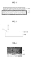
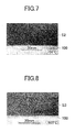
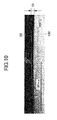
- FIG. 2 to Fig. 4 are views illustrating an example of manufacturing steps of the CIS-based compound thin-film photovoltaic cell of the embodiment.
- the metal substrate 11 is prepared.
- the metal substrate 11 is a substrate whose main constituent is iron and containing aluminium (Al) and chromium (Cr).
- a ferrite-based stainless substrate containing aluminium (Al) is used as the metal substrate 11.
- the content of aluminium (Al) in the metal substrate 11 is greater than or equal to 0.5 weight % and less than or equal to 6.0 weight %.
- the thickness of the metal substrate 11 may be about 0.2 mm to 0.6 mm, for example.
- the metal substrate 11 is baked (heated and oxidized, in other words, thermal oxidation) at temperature (this temperature may be referred to as pretreatment temperature) greater than or equal to 700 °C and less than 850 °C under air or atmosphere including oxygen to form the alumina layer 12 by diffusing aluminium (Al) included in the metal substrate 11 to the entire surface of the metal substrate 11.
- the alumina layer 12 may be at least formed on the upper surface (element forming surface) of the metal substrate 11. This is because the adhesion between the alumina layer 12 formed on the upper surface of the metal substrate 11 and the insulating layer 13 that is formed right above the alumina layer 12 can be improved.
- the point that it is preferable that the pretreatment temperature is greater than or equal to 700 °C and less than 850 °C was experimentally found by the present inventors. According to the studies by the present inventors, when the pretreatment temperature is less than 700 °C, the adhesion between the insulating layer 13 is lowered because the alumina layer 12 is not sufficiently formed on the upper surface of the metal substrate 11. Further, if the pretreatment temperature is greater than or equal to 850 °C, the heat deformation amount of the metal substrate 11 becomes large and it becomes improper for the substrate of the compound thin-film photovoltaic cell, for which flatness is required. Further, there are other problems such as that a specific facility for heating is necessary and energy consumption for the heat treatment is large.
- waviness which is a difference of elevation of concavo-convex when the metal substrate 11 is placed on plane, largely exceeds an allowable value (less than or equal to 1 mm) of the substrate for the compound thin-film photovoltaic cell.
- the pretreatment temperature is greater than or equal to 700 °C and less than 850 °C
- the alumina layer 12 with the thickness sufficient to improve the adhesion with the insulating layer 13 that is directly formed thereon can be formed and the "waviness" of the metal substrate 11 can be suppressed to a value less than or equal to the allowable value (less than or equal to 1 mm) of the substrate for the compound thin-film photovoltaic cell.
- temperature greater than or equal to 700 °C and less than 850 °C is lower than general pretreatment temperature (greater than or equal to 850 °C and less than about 1100 °C) for forming an alumina layer, it is possible to reduce baking energy as well.
- the metal substrate 11 may be configured as a continuous substrate including a plurality of regions, each of which becomes the substrate of the photovoltaic cell when being individualized, and the alumina layer may be continuously formed at least on the element forming surface of the plurality of regions.
- the continuous substrate may be continuously baked by a roll-to-roll process to form the alumina layer 12, and the substrate may be cut to be individualized thereafter.
- the continuous substrate may be cut to be individualized after the alumina layer 12 is formed, or after other layers are formed thereon.
- the insulating layer 13 is formed on the alumina layer 12 that is formed on the upper surface of the metal substrate 11.
- glass paste whose softening point is within 600 °C to 800 °C is coated on the alumina layer 12 that is formed on the upper surface of the metal substrate 11.
- the glass paste may be coated by a slit coater, for example.
- the glass paste may be coated by a spray coater, screen printing, a dip coater, a spin coater or the like.
- the coated glass paste is heated at about 100 °C to 200 °C in air to dry the glass paste and vaporize organic solvent in the glass paste. Further, by heating and baking the dried glass paste at temperature greater than or equal to the softening point, the insulating layer 13 is formed. It is preferable that the thickness of the insulating layer 13 after being baked is greater than or equal to 10 ⁇ m and less than or equal to 50 ⁇ m, and for example, may be about 30 ⁇ m.
- temperatures for the step of drying the glass paste and the step of heating and baking the glass paste are largely different, those steps may be performed in different apparatuses.
- the insulating layer 13 may be formed by a plurality of layers, and in such a case, the insulating layer 13 may include a layer that has the alkali barrier function.
- Both the insulating layer 13 and the alumina layer 12 are layers made of oxide (oxide layers). As oxides have compatibility with each other, the adhesion between the insulating layer 13 and the alumina layer 12 is improved compared with a case when the insulating layer 13 is directly formed on the metal substrate 11 on which the alumina layer 12 is not formed (a case when the insulating layer 13 is directly formed on the metal substrate 11, which is not oxide).
- the element forming surface of the metal substrate 11 is covered by extremely thin chromium oxide.
- the insulating layer 13 is directly formed on chromium oxide, it may be considered that an improvement effect of the adhesion due to oxides can be obtained.
- chromium oxide is extremely thin (about a few nm to 10 nm, for example), the improvement effect of the adhesion cannot be obtained at all.
- the thickness of the alumina layer 12 that covers the element forming surface of the metal substrate 11 is greater than or equal to 30 nm (in some cases, about 1 ⁇ m), which is far thicker than the thickness of chromium oxide (about a few nm to 10 nm, for example), the adhesion with the insulating layer 13 can be improved due to the compatibility of oxides. As such, the improvement effect of the adhesion between oxides occurs more as the thickness becomes thicker.
- the alumina layer 12 is integrally formed by diffusing aluminium (Al) included in the metal substrate 11, not formed by a method such as depositing alumina on the upper surface of the metal substrate 11.
- Al diffusing aluminium
- the insulating layer 13 is an oxide layer
- good adhesion with the alumina layer 12 can be obtained even when the insulating layer 13 is a nitride layer composed of silicon nitride or the like, similar for the case when the insulating layer 13 is the oxide layer.
- the insulating layer 13 composed of silicon nitride may be formed on the alumina layer 12 by reactive sputtering between silicon and nitrogen, a plasma CVD method or the like, for example.
- the compound thin-film photovoltaic cell 10 illustrated in Fig. 1 is completed by stacking the first electrode layer 14, the compound light absorption layer 15 and the second electrode layer 16 on the insulating layer 13 in this order, after the steps illustrated in Fig. 4 .
- the first electrode layer 14 is deposited on the insulating layer 13 by a DC magnetron sputtering method or the like, for example.
- the first electrode layer 14 may be deposited on the insulating layer 13 by an electron beam evaporation method or the like.
- the material, the thickness or the like of the first electrode layer 14 is as described above.
- an alkali barrier layer may be formed by a sputtering method or the like.
- the material, the thickness or the like of the alkali barrier layer is as described above.
- Copper indium gallium 2 sulfide-selenide (Cu(InGa)(SSe) 2 ) is deposited on the first electrode layer 14 as the compound light absorption layer 15.
- Copper indium gallium 2 sulfide-selenide (Cu(InGa)(SSe) 2 ) may be deposited by forming a precursor film including copper (Cu), gallium (Ga), indium (In) and the like by a DC magnetron sputtering method, an evaporation method or the like, for example, and thereafter, introducing selenide by hydrogen selenide (H 2 Se) and sulfide by hydrogen sulfide (H 2 S) (introduction process of selenide/ sulfide) at temperature about 400 to 600 °C, for example.
- H 2 Se hydrogen selenide
- H 2 S hydrogen sulfide
- CuInGa copper indium gallium 2 sulfide-selenide
- CuInSe 2 copper indium 2 selenide
- CuInS 2 copper indium 2 sulfide
- the compound light absorption layer 15 may be deposited by vapor depositing copper (Cu), gallium (Ga), indium (In) and selenium (Se). Further, the compound light absorption layer 15 may be deposited by vapor depositing copper (Cu), gallium (Ga), indium (In) and sulfur (S). Further, the compound light absorption layer 15 may be deposited by vapor depositing copper (Cu), gallium (Ga), indium (In), selenium (Se) and sulfur (S).
- the compound light absorption layer 15 may be deposited by a sputtering method, a hybrid sputtering method, a mechanochemical process method, a screen printing method, a close-spaced sublimation method, a MOCVD method, a spraying method or the like.
- the entire surface of the metal substrate 11 is covered by the alumina layer 12, corrosion of the entire surface of the metal substrate 11 due to hydrogen selenide (H 2 Se), hydrogen sulfide (H 2 S) or the like can be suppressed.
- H 2 Se hydrogen selenide
- H 2 S hydrogen sulfide
- a buffer layer may be deposited on the compound light absorption layer 15.
- the buffer layer may be deposited on the compound light absorption layer 15 by a Chemical Bath Deposition method (CBD method), a Metal Organic Chemical Vapor Deposition method (MOCVD method), an Atomic Layer Deposition method (ALD method) or the like, for example.
- CBD method Chemical Bath Deposition method
- MOCVD method Metal Organic Chemical Vapor Deposition method
- ALD method Atomic Layer Deposition method
- the material, the thickness or the like of the buffer layer is as described above.
- the second electrode layer 16 is deposited on the compound light absorption layer 15 by a MOCVD method or the like, for example.
- the second electrode layer 16 may be formed on the compound light absorption layer 15 using a sputtering method, an evaporation method, an Atomic Layer Deposition method (ALD method) or the like.
- the material, the thickness or the like of the second electrode layer 16 is as described above.
- separating grooves may be formed in the first electrode layer 14, the compound light absorption layer 15 and the second electrode layer 16 and may form an integrated structure in which cells, which are separated and formed into strip shapes by the separating grooves separating grooves, are connected in series.
- the alumina layer 12 is formed at least on the element forming surface of the metal substrate 11 and the insulating layer 13 is formed right about the alumina layer 12.
- an anchor effect is generated between the metal substrate 11 and the alumina layer 12 and the adhesion therebetween can be improved.
- the alumina layer 12 that is an oxide layer and the insulating layer 13 that is an oxide layer or a nitride layer are compatible with each other and the adhesion therebetween can be improved due to this reason.
- the adhesion between the metal substrate 11 and the insulating layer 13 can be improved and the delamination between the metal substrate 11 and the insulating layer 13 can be suppressed.
- the compound thin-film photovoltaic cell 10 with good characteristics can be manufactured.
- pretreatment temperature when forming the alumina layer 12 is greater than or equal to 700 °C and less than 850 °C, which is lower than general pretreatment temperature (about greater than or equal to 850 °C and less than 1100 °C), baking energy can be reduced.
- the alumina layer 12 and the insulating layer 13 exist between the element forming surface of the metal substrate 11 and the lower surface of the first electrode layer 14. This means that as the metal substrate 11 and the first electrode layer 14 are separated by an insulating body of the two-layered structure including the stacked alumina layer 12 and the insulating layer 13, withstand voltage between the metal substrate 11 and the first electrode layer 14 can be improved.
- Example 1 a surface condition of the alumina layer 12 and deformation (warp or waviness) of the metal substrate 11 were confirmed.
- ferrite-based stainless substrates each containing aluminium (Al) JFE18-3USR: a ferrite-based stainless substrate containing 3.4% of aluminium
- a plurality of samples were manufactured by performing pretreatment on each of the metal substrates 11 to form the alumina layer 12 at the entire surface of each of the metal substrates 11.
- three kinds of samples were manufactured including sample 1 for which the pretreatment temperature was 700 °C, sample 2 for which the pretreatment temperature was 750 °C and sample 3 for which the pretreatment temperature was 800 °C.
- the thickness of the alumina layer 12 was about 30 nm to 100 nm.
- the insulating layer 13 or the like was not stacked on the alumina layer 12.
- samples 1 to 3 (indicated as S1 to S3, respectively, in Fig. 5 ) in each of which the alumina layer 12 was formed at the entire surface of the metal substrate 11, were placed on an orientation plate 100 (a flat plate) in order, photographed from a direction of an arrow A (from upper side), and a surface condition of each of the samples was confirmed ( Fig. 6 to Fig. 8 ).
- Fig. 6 illustrates a picture indicting the surface condition of sample 1
- Fig. 7 illustrates a picture indicting the surface condition of sample 2
- Fig. 8 illustrates a picture indicting the surface condition of sample 3.
- the lower side of the respective drawing is the orientation plate 100 and the upper side of the respective drawing is each of samples 1 to 3 (illustrated as S1 to S3 in Fig. 6 to Fig. 8 , respectively) in which the alumina layer 12 is formed at the entire surface of the metal substrate 11.
- a uniform alumina layer 12 was formed in each of samples.
- the length of the straight line illustrated in the orientation plate 100 corresponds to 30 mm.
- sample 9 was manufactured in which the alumina layer 12 is formed at the entire surface of the metal substrate 11 by performing pretreatment at pretreatment temperature of 900 °C on the prepared metal substrate 11. Then, samples 3 and 9 are placed on the orientation plate 100 (a flat plate) in order, photographed from a direction of an arrow B (from inclined upper side) in Fig. 5 , and deformation (warp, waviness) of the metal substrate 11 of each of the samples was confirmed ( Fig. 9 and Fig. 10 ).
- Fig. 9 illustrates a picture of the metal substrate 11 of sample 3
- Fig. 10 illustrates a picture of the metal substrate 11 of sample 9.
- the lower side of the respective drawing is the orientation plate 100 and the upper side of the respective drawing is each of samples 3 and 9 (illustrated as S3 in Fig. 9 and S9 in Fig. 10 ) in which the alumina layer 12 is formed at the entire surface of the metal substrate 11.
- the length of the straight line illustrated in the orientation plate 100 corresponds to 100 mm.
- Example 2 whether delamination occurred at an interface between the alumina layer 12 and the insulating layer 13 was confirmed.
- the metal substrate 11 similar to that of Example 1 was prepared.
- pretreatment was performed on the prepared metal substrate 11, and a plurality of samples in each of which the alumina layer 12 was formed at the entire surface of the metal substrate 11 were prepared. Specifically, two kinds of samples were prepared including sample 4 in which the pretreatment temperature was 750 °C and sample 5 in which the pretreatment temperature was 800 °C. In each of samples 4 and 5, the thickness of the alumina layer 12 was about 30 nm to 100 nm.
- the insulating layer 13 was stacked on the alumina layer 12 of each of samples 4 and 5 by a glass. Thereafter, the interface of the alumina layer 12 and the insulating layer 13 was observed for each of samples 4 and 5 and no delamination was confirmed for both the cases.
Landscapes
- Photovoltaic Devices (AREA)
- Engineering & Computer Science (AREA)
- Life Sciences & Earth Sciences (AREA)
- Sustainable Energy (AREA)
- Sustainable Development (AREA)
- Manufacturing & Machinery (AREA)
Applications Claiming Priority (2)
| Application Number | Priority Date | Filing Date | Title |
|---|---|---|---|
| JP2012286186A JP2014127711A (ja) | 2012-12-27 | 2012-12-27 | 化合物系薄膜太陽電池及びその製造方法 |
| PCT/JP2013/082883 WO2014103669A1 (fr) | 2012-12-27 | 2013-12-06 | Cellule solaire à couches minces à base de composé, et procédé de fabrication de celle-ci |
Publications (2)
| Publication Number | Publication Date |
|---|---|
| EP2940736A1 true EP2940736A1 (fr) | 2015-11-04 |
| EP2940736A4 EP2940736A4 (fr) | 2015-12-23 |
Family
ID=51020761
Family Applications (1)
| Application Number | Title | Priority Date | Filing Date |
|---|---|---|---|
| EP13866575.7A Withdrawn EP2940736A4 (fr) | 2012-12-27 | 2013-12-06 | Cellule solaire à couches minces à base de composé, et procédé de fabrication de celle-ci |
Country Status (4)
| Country | Link |
|---|---|
| US (1) | US20150340535A1 (fr) |
| EP (1) | EP2940736A4 (fr) |
| JP (1) | JP2014127711A (fr) |
| WO (1) | WO2014103669A1 (fr) |
Families Citing this family (2)
| Publication number | Priority date | Publication date | Assignee | Title |
|---|---|---|---|---|
| JP5997044B2 (ja) * | 2012-12-27 | 2016-09-21 | ソーラーフロンティア株式会社 | 化合物系薄膜太陽電池の製造方法 |
| CN114759106B (zh) * | 2021-01-12 | 2024-03-08 | 宝山钢铁股份有限公司 | 一种适用于内联式薄膜光伏组件的涂镀钢板及其制造方法 |
Family Cites Families (8)
| Publication number | Priority date | Publication date | Assignee | Title |
|---|---|---|---|---|
| JPS63155681A (ja) | 1986-12-18 | 1988-06-28 | Kawasaki Steel Corp | 太陽電池基板用母板の製造方法 |
| JP2004158511A (ja) * | 2002-11-01 | 2004-06-03 | Matsushita Electric Ind Co Ltd | 太陽電池用基板およびその製造方法ならびにそれを用いた太陽電池 |
| JP2004327850A (ja) * | 2003-04-25 | 2004-11-18 | Matsushita Electric Ind Co Ltd | 集積型太陽電池 |
| JP2010212336A (ja) * | 2009-03-09 | 2010-09-24 | Fujifilm Corp | 光電変換素子とその製造方法、及び太陽電池 |
| JP2010263037A (ja) * | 2009-05-01 | 2010-11-18 | Fujifilm Corp | 金属複合基板およびその製造方法 |
| JP2011176288A (ja) * | 2010-02-01 | 2011-09-08 | Fujifilm Corp | 光電変換素子、薄膜太陽電池および光電変換素子の製造方法 |
| JP5634315B2 (ja) * | 2010-04-07 | 2014-12-03 | 富士フイルム株式会社 | 絶縁層付金属基板および光電変換素子 |
| US20120006395A1 (en) * | 2010-07-08 | 2012-01-12 | E. I. Du Pont De Nemours And Company | Coated stainless steel substrate |
-
2012
- 2012-12-27 JP JP2012286186A patent/JP2014127711A/ja active Pending
-
2013
- 2013-12-06 EP EP13866575.7A patent/EP2940736A4/fr not_active Withdrawn
- 2013-12-06 WO PCT/JP2013/082883 patent/WO2014103669A1/fr not_active Ceased
- 2013-12-06 US US14/654,870 patent/US20150340535A1/en not_active Abandoned
Also Published As
| Publication number | Publication date |
|---|---|
| WO2014103669A1 (fr) | 2014-07-03 |
| EP2940736A4 (fr) | 2015-12-23 |
| US20150340535A1 (en) | 2015-11-26 |
| JP2014127711A (ja) | 2014-07-07 |
Similar Documents
| Publication | Publication Date | Title |
|---|---|---|
| US7741560B2 (en) | Chalcopyrite solar cell | |
| JP4629151B2 (ja) | 光電変換素子及び太陽電池、光電変換素子の製造方法 | |
| US9166077B2 (en) | Thin film solar cell | |
| CN103329277B (zh) | 用于光伏电池的导电基材 | |
| US20100319777A1 (en) | Solar cell and method of fabricating the same | |
| KR101172132B1 (ko) | 태양전지 및 이의 제조방법 | |
| CN102057496B (zh) | 对于能收集光元件的改进 | |
| JP2004047860A (ja) | 薄膜太陽電池およびその製造方法 | |
| JP6104576B2 (ja) | 化合物系薄膜太陽電池 | |
| EP2940736A1 (fr) | Cellule solaire à couches minces à base de composé, et procédé de fabrication de celle-ci | |
| EP2983211A1 (fr) | Cellule solaire à pellicule mince | |
| US7923628B2 (en) | Method of controlling the composition of a photovoltaic thin film | |
| JP2011009287A (ja) | Cis系薄膜太陽電池 | |
| US9472698B2 (en) | Method of manufacturing compound thin-film photovoltaic cell | |
| KR101034146B1 (ko) | 태양전지 및 이의 제조방법 | |
| JP6104579B2 (ja) | 薄膜太陽電池の製造方法 | |
| KR20200097118A (ko) | Cigs 박막 태양전지 제조방법 | |
| WO2025057654A1 (fr) | Cellule solaire et procédé de fabrication de cellule solaire | |
| JP2014090009A (ja) | 光電変換装置 |
Legal Events
| Date | Code | Title | Description |
|---|---|---|---|
| PUAI | Public reference made under article 153(3) epc to a published international application that has entered the european phase |
Free format text: ORIGINAL CODE: 0009012 |
|
| 17P | Request for examination filed |
Effective date: 20150624 |
|
| AK | Designated contracting states |
Kind code of ref document: A1 Designated state(s): AL AT BE BG CH CY CZ DE DK EE ES FI FR GB GR HR HU IE IS IT LI LT LU LV MC MK MT NL NO PL PT RO RS SE SI SK SM TR |
|
| AX | Request for extension of the european patent |
Extension state: BA ME |
|
| A4 | Supplementary search report drawn up and despatched |
Effective date: 20151125 |
|
| RIC1 | Information provided on ipc code assigned before grant |
Ipc: H01L 31/0392 20060101ALI20151119BHEP Ipc: H01L 31/0749 20120101ALI20151119BHEP Ipc: H01L 31/06 20120101AFI20151119BHEP Ipc: C03C 1/00 20060101ALI20151119BHEP |
|
| DAX | Request for extension of the european patent (deleted) | ||
| STAA | Information on the status of an ep patent application or granted ep patent |
Free format text: STATUS: EXAMINATION IS IN PROGRESS |
|
| 17Q | First examination report despatched |
Effective date: 20180709 |
|
| STAA | Information on the status of an ep patent application or granted ep patent |
Free format text: STATUS: THE APPLICATION HAS BEEN WITHDRAWN |
|
| 18W | Application withdrawn |
Effective date: 20180821 |