EP2940738B1 - Élément de cellule solaire et procédé de fabrication d'un élément de cellule solaire - Google Patents
Élément de cellule solaire et procédé de fabrication d'un élément de cellule solaire Download PDFInfo
- Publication number
- EP2940738B1 EP2940738B1 EP13867996.4A EP13867996A EP2940738B1 EP 2940738 B1 EP2940738 B1 EP 2940738B1 EP 13867996 A EP13867996 A EP 13867996A EP 2940738 B1 EP2940738 B1 EP 2940738B1
- Authority
- EP
- European Patent Office
- Prior art keywords
- region
- concentration
- semiconductor substrate
- line
- concentration region
- Prior art date
- Legal status (The legal status is an assumption and is not a legal conclusion. Google has not performed a legal analysis and makes no representation as to the accuracy of the status listed.)
- Active
Links
Images


Classifications
-
- H—ELECTRICITY
- H10—SEMICONDUCTOR DEVICES; ELECTRIC SOLID-STATE DEVICES NOT OTHERWISE PROVIDED FOR
- H10F—INORGANIC SEMICONDUCTOR DEVICES SENSITIVE TO INFRARED RADIATION, LIGHT, ELECTROMAGNETIC RADIATION OF SHORTER WAVELENGTH OR CORPUSCULAR RADIATION
- H10F10/00—Individual photovoltaic cells, e.g. solar cells
- H10F10/10—Individual photovoltaic cells, e.g. solar cells having potential barriers
- H10F10/13—Photovoltaic cells having absorbing layers comprising graded bandgaps
-
- H—ELECTRICITY
- H10—SEMICONDUCTOR DEVICES; ELECTRIC SOLID-STATE DEVICES NOT OTHERWISE PROVIDED FOR
- H10F—INORGANIC SEMICONDUCTOR DEVICES SENSITIVE TO INFRARED RADIATION, LIGHT, ELECTROMAGNETIC RADIATION OF SHORTER WAVELENGTH OR CORPUSCULAR RADIATION
- H10F10/00—Individual photovoltaic cells, e.g. solar cells
- H10F10/10—Individual photovoltaic cells, e.g. solar cells having potential barriers
- H10F10/14—Photovoltaic cells having only PN homojunction potential barriers
-
- H—ELECTRICITY
- H10—SEMICONDUCTOR DEVICES; ELECTRIC SOLID-STATE DEVICES NOT OTHERWISE PROVIDED FOR
- H10F—INORGANIC SEMICONDUCTOR DEVICES SENSITIVE TO INFRARED RADIATION, LIGHT, ELECTROMAGNETIC RADIATION OF SHORTER WAVELENGTH OR CORPUSCULAR RADIATION
- H10F71/00—Manufacture or treatment of devices covered by this subclass
- H10F71/121—The active layers comprising only Group IV materials
-
- H—ELECTRICITY
- H10—SEMICONDUCTOR DEVICES; ELECTRIC SOLID-STATE DEVICES NOT OTHERWISE PROVIDED FOR
- H10F—INORGANIC SEMICONDUCTOR DEVICES SENSITIVE TO INFRARED RADIATION, LIGHT, ELECTROMAGNETIC RADIATION OF SHORTER WAVELENGTH OR CORPUSCULAR RADIATION
- H10F71/00—Manufacture or treatment of devices covered by this subclass
- H10F71/128—Annealing
-
- H—ELECTRICITY
- H10—SEMICONDUCTOR DEVICES; ELECTRIC SOLID-STATE DEVICES NOT OTHERWISE PROVIDED FOR
- H10F—INORGANIC SEMICONDUCTOR DEVICES SENSITIVE TO INFRARED RADIATION, LIGHT, ELECTROMAGNETIC RADIATION OF SHORTER WAVELENGTH OR CORPUSCULAR RADIATION
- H10F77/00—Constructional details of devices covered by this subclass
- H10F77/20—Electrodes
- H10F77/206—Electrodes for devices having potential barriers
- H10F77/211—Electrodes for devices having potential barriers for photovoltaic cells
-
- Y—GENERAL TAGGING OF NEW TECHNOLOGICAL DEVELOPMENTS; GENERAL TAGGING OF CROSS-SECTIONAL TECHNOLOGIES SPANNING OVER SEVERAL SECTIONS OF THE IPC; TECHNICAL SUBJECTS COVERED BY FORMER USPC CROSS-REFERENCE ART COLLECTIONS [XRACs] AND DIGESTS
- Y02—TECHNOLOGIES OR APPLICATIONS FOR MITIGATION OR ADAPTATION AGAINST CLIMATE CHANGE
- Y02E—REDUCTION OF GREENHOUSE GAS [GHG] EMISSIONS, RELATED TO ENERGY GENERATION, TRANSMISSION OR DISTRIBUTION
- Y02E10/00—Energy generation through renewable energy sources
- Y02E10/50—Photovoltaic [PV] energy
- Y02E10/547—Monocrystalline silicon PV cells
-
- Y—GENERAL TAGGING OF NEW TECHNOLOGICAL DEVELOPMENTS; GENERAL TAGGING OF CROSS-SECTIONAL TECHNOLOGIES SPANNING OVER SEVERAL SECTIONS OF THE IPC; TECHNICAL SUBJECTS COVERED BY FORMER USPC CROSS-REFERENCE ART COLLECTIONS [XRACs] AND DIGESTS
- Y02—TECHNOLOGIES OR APPLICATIONS FOR MITIGATION OR ADAPTATION AGAINST CLIMATE CHANGE
- Y02P—CLIMATE CHANGE MITIGATION TECHNOLOGIES IN THE PRODUCTION OR PROCESSING OF GOODS
- Y02P70/00—Climate change mitigation technologies in the production process for final industrial or consumer products
- Y02P70/50—Manufacturing or production processes characterised by the final manufactured product
Definitions
- the present invention relates to a solar cell element and a method for manufacturing the solar cell element.
- a solar cell element has been known in which a region (reverse conductivity type region) where a reverse conductivity type impurity element is introduced is provided in a surface layer portion of a front surface in a one conductivity type semiconductor substrate, in which an anti-reflection film and an electrode in line shape are placed on the region, and in which an electrode is placed on a rear surface of the semiconductor substrate.
- a solar cell element is suggested, the solar cell element having a structure (selective emitter structure) in which a content concentration of the reverse conductivity type impurity element is increased in the region where the electrode in line shape is placed in the reverse conductivity type region.
- the selective emitter structure is formed as follows. First, a p-type semiconductor substrate is disposed in a heating furnace as the one conductivity type semiconductor substrate. Next, in a state where the semiconductor substrate is heated, gas which contains an n-type impurity element as a reverse conductivity type is supplied to the inside of the heating furnace, and thereby the n-type impurity element is introduced into the surface layer portion of the p-type semiconductor substrate by diffusion. At this time, a first emitter region is formed in the surface layer portion of the p-type semiconductor substrate, and a layer (for example, phosphosilicate glass layer) which is a diffusion source of the n-type impurity element is formed on the first emitter region.
- a layer for example, phosphosilicate glass layer
- the diffusion source When a preset position of the diffusion source is selectively irradiated with laser light, the diffusion source is locally heated, and the n-type impurity element is further introduced into the semiconductor substrate by diffusion. Accordingly, in the region where the electrode in line shape is placed, a second emitter region where a content concentration of the n-type impurity element as the reverse conductivity type is increased is formed.
- one main surface of the p-type semiconductor substrate as the one conductivity type is coated with a paste-formed raw material solution (for example, P 2 O 5 ) which contains the n-type impurity element as the reverse conductivity type. Subsequently, a heat treatment is performed, thereby forming a reverse conductivity region is formed in the surface layer portion of the p-type semiconductor substrate.
- a paste-formed raw material solution for example, P 2 O 5
- a concentration of a reverse conductivity type impurity element varies in the first emitter region and a thickness of the first emitter region varies.
- a sheet resistance in the first emitter region varies.
- the concentration of the reverse conductivity type impurity element varies in the first emitter region, the thickness of the first emitter region varies, and a thickness of a diffusion source varies, due to a decrease in the gas concentration and the substrate temperature.
- a concentration and a thickness of a reverse conductivity type impurity element in a second emitter region vary. Accordingly, a sheet resistance in the second emitter region increases, and a pn junction depth may be less than an optimum value. In other words, for example, a contact resistance in a boundary part between the semiconductor substrate and an electrode in line shape increases, and the pn junction depth becomes less than the optimum value. As a result, an FF and an open-circuit voltage in a solar cell element decrease, and conversion efficiency in the solar cell element decreases.
- a solar cell element which can improve the conversion efficiency by improving the boundary part between the semiconductor substrate and the electrode and a method for manufacturing the solar cell element are desired.
- a solar cell element includes: a semiconductor substrate which includes a first conductivity type first semiconductor region positioned on a first main surface, and a second conductivity type second semiconductor region which is different from the first conductivity type in a surface layer portion of a second main surface positioned on an opposite side to the first main surface; and an electrode in line shape which is disposed on the second main surface of the semiconductor substrate.
- the second semiconductor region includes a first concentration region which exists at a position separated from the electrode by a predetermined distance in plan view, and a second concentration region which includes a high concentration region where a dopant concentration is higher than that in the first concentration region and exists along a longitudinal direction of the electrode.
- the solar cell element includes a part in which a minimum place which has a minimum value of a dopant concentration difference that is obtained by subtracting a dopant concentration value of the first concentration region at a place which is close to a one place from a dopant concentration value of the second concentration region at the one place and a maximum place which has a maximum value of the dopant concentration difference alternately and repeatedly exist, along the longitudinal direction of the electrode, and in which a minimum place interval between one end portions of the adjacent minimum places in the longitudinal direction of the electrode varies.
- a method for manufacturing a solar cell element includes: a preparation process of preparing a first conductivity type semiconductor substrate; a first forming process of forming a second conductivity type first concentration region where a second conductivity type dopant concentration is in a first concentration range, by diffusing an element which becomes the second conductivity type dopant that is different from the first conductivity type, in a surface layer portion of one main surface of the first semiconductor substrate; a second forming process of forming a second conductivity type second concentration region which includes a high concentration region having the second conductivity type dopant concentration in a second concentration range that is higher than the first concentration range, by diffusing the element which becomes the second conductivity type dopant, in the surface layer portion of the semiconductor substrate from an element supply source, by irradiating the element supply source with laser light at a periodic timing, in a state where the element supply source containing the element which becomes the second conductivity type dopant is placed on the first concentration region; and a third forming process of forming an electrode on the second
- this manufacturing method changes at least one condition among three conditions of an interval between center positions of the irradiation target regions, an area of the irradiation target region, and a radiation energy of the laser light for the irradiation target region.
- a dopant concentration in a second concentration region which is formed by allowing a part having a relatively low dopant concentration in a first concentration region to be a base portion can appropriately increase, a distribution of a sheet resistance in the second concentration region can be narrow and can be settled in an appropriate value range. As a result, by improving a boundary part between a semiconductor substrate and an electrode, it is possible to improve conversion efficiency.
- a sheet resistance in a second concentration region which is formed by allowing a part having a relatively high sheet resistance in a first concentration region to be a base portion can appropriately decrease, a distribution of a sheet resistance in the second concentration region can be narrow and can be settled in an appropriate value range.
- a boundary part between a semiconductor substrate and an electrode it is possible to improve conversion efficiency.
- the solar cell element 10 includes a first main surface 10a, a second main surface 10b, and a side surface 10c.
- the second main surface 10b is a surface (light receiving surface) which receives incident light.
- the first main surface 10a is a surface (non-light-receiving surface) which is positioned on an opposite side to the second main surface 10b in the solar cell element 10.
- the side surface 10c is a surface which connects the first main surface 10a and the second main surface 10b to each other.
- the first main surface 10a is drawn as a lower surface on a -Z side of the solar cell element 10
- the second main surface 10b is drawn as an upper surface on a +Z side of the solar cell element 10.
- the solar cell element 10 includes a semiconductor substrate 1 in a plate shape, an anti-reflection film 2, a first electrode 4, and a second electrode 5.
- the semiconductor substrate 1 has a configuration in which a first conductivity type first semiconductor region 1p and a second conductivity type second semiconductor region In which is different from the first conductivity type are stacked.
- the first semiconductor region 1p is positioned on the first main surface 10a side (-Z side in the drawing) in the semiconductor substrate 1.
- the second semiconductor region In is positioned in a surface layer portion on the second main surface 10b side (+Z side in the drawing) which is opposite to the first main surface 10a side in the semiconductor substrate 1.
- the semiconductor substrate 1 has a plate shape which has a rectangular surface.
- the semiconductor substrate 1 is a monocrystal or polycrystal silicon substrate (crystal silicon substrate).
- the first conductivity type and the second conductivity type may be conductivity types which are reverse to each other.
- the first conductivity type is a p-type
- the second conductivity type is an n-type.
- the first conductivity type is the n-type
- the second conductivity type is the p-type. Accordingly, the first semiconductor region 1p and the second semiconductor region In form a pn junction region.
- the first conductivity type is the p-type
- the second conductivity type is the n-type.
- the first semiconductor region 1p is a p-type semiconductor region.
- the second semiconductor region In is an n-type semiconductor region.
- One side of the plate surface of the semiconductor substrate 1 may be 156 mm, for example.
- a thickness of the first semiconductor region 1p may be equal to or less than 250 ⁇ m, for example, and further, may be equal to or less than 150 ⁇ m.
- the shape of the semiconductor substrate 1 is not particularly limited, but, for example, if the shape is rectangular in plan view, it is easy to manufacture the semiconductor substrate 1.
- the second semiconductor region In includes a first concentration region 1Ln and a second concentration region 1Hn.
- the first concentration region 1Ln is a semiconductor region where a concentration (dopant concentration) of an n-type dopant as the second conductivity type is in a first concentration range.
- the n-type dopant concentration in the second concentration region 1Hn is higher than the n-type dopant concentration in the first concentration region 1Ln.
- the second semiconductor region In is formed in the surface layer portion on a second main surface 1b side in the crystal silicon substrate by introducing an element which becomes the n-type dopant into a region on the second main surface 1b side in the p-type crystal silicon substrate, by diffusion.
- a part other than the second semiconductor region In in the crystal silicon substrate becomes the first semiconductor region 1p.
- the n-type dopant for example, a phosphorus (P) is employed.
- the first semiconductor region 1p includes a third concentration region 1Lp and a fourth concentration region 1Hp.
- the fourth concentration region 1Hp is positioned in the surface layer portion on a first main surface 1a side in the semiconductor substrate 1.
- the fourth concentration region 1Hp includes a gap which allows an output extraction electrode 4b and the third concentration region 1Lp to be in contact with each other on the first main surface 1a.
- the p-type dopant concentration in the fourth concentration region 1Hp is higher than the p-type dopant concentration in the third concentration region 1Lp.
- the p-type dopant for example, boron (B), gallium (Ga), or aluminum (Al) is employed.
- the fourth concentration region 1Hp has a role of reducing recombination of carriers in the region on the first main surface 1a side in the semiconductor substrate 1. Accordingly, since the fourth concentration region 1Hp exists, decrease of conversion efficiency is suppressed in the solar cell element 10.
- the fourth concentration region 1Hp an internal electric field is generated on the first main surface 1a side in the semiconductor substrate 1.
- the fourth concentration region 1Hp is formed by introducing the dopant, such as B or A1, into the region on the first main surface 1a side in the semiconductor substrate 1, by diffusion. In this case, a part other than the fourth concentration region 1Hp in the first semiconductor region 1p becomes the third concentration region 1Lp.
- a projection and recess portion 1bL is placed across the substantially entire second main surface 1b in the semiconductor substrate 1.
- a height of a projection portion in the projection and recess portion 1bL are approximately equal to or greater than 0.1 ⁇ m and equal to or less than 10 ⁇ m, for example.
- a width of the projection portion is approximately equal to or greater than 0.1 ⁇ m and equal to or less than 20 ⁇ m, for example.
- a surface shape of a recess portion of the projection and recess portion 1bL may be, for example, substantially spherical.
- the above-described height of the projection portion is considered to be a distance from a reference surface to a top surface of the projection portion in a normal line direction of the reference surface.
- the reference surface is a surface which passes through a bottom surface of the recess portion and is parallel to the first main surface 1a.
- the above-described width of the projection portion means a distance between the top surfaces of the adjacent projection portions in a direction which is parallel to the above-described reference surface. Since the projection and recess portion 1bL exists, reflectance is reduced in the second main surface 1b on the light receiving surface side of the semiconductor substrate 1.
- alignment reference portions 1m are provided to be separated from each other at two or more locations.
- the alignment reference portions 1m at two or more locations are used as a reference when adjusting a position where the second electrode 5 is formed.
- the alignment reference portions 1m are placed at two locations on the second main surface 1b, but the embodiment is not limited thereto.
- the alignment reference portions 1m may be placed at three or more locations on the second main surface 1b.
- the anti-reflection film 2 is a film for improving light absorption efficiency in the solar cell element 10.
- the anti-reflection film 2 is placed on the first concentration region 1Ln on the second main surface 1b side in the semiconductor substrate 1.
- a material of the anti-reflection film 2 for example, a silicon nitride, a titanium oxide, a silicon oxide, a magnesium oxide, an indium tin oxide, a tin oxide, a zinc oxide or the like is employed.
- a silicon nitride film is employed as the anti-reflection film 2 since the anti-reflection film 2 functions as a passivation film, a passivation effect is realized.
- the upper surface on the +Z side of the anti-reflection film 2 includes a projection and recess portion according to the shape of the projection and recess portion 1bL.
- a thickness of the anti-reflection film 2 may be appropriately set in accordance with materials of the semiconductor substrate 1 and anti-reflection film 2. Accordingly, in the solar cell element 10, a condition that light is unlikely to be reflected with respect to various types of light radiation is realized.
- a refractive index of the anti-reflection film 2 is approximately equal to or greater than 1.8 and equal to or less than 2.3, for example, and it is sufficient that a thickness of the anti-reflection film 2 is approximately equal to or greater than 50 nm and equal to or less than 120 nm, for example.
- the first electrode 4 is placed on the first main surface 1a of the semiconductor substrate 1. As illustrated in Figs. 2 and 3 , the first electrode 4 includes a collection electrode 4a and the output extraction electrode 4b.
- the collection electrode 4a is placed on the fourth concentration region 1Hp. Specifically, for example, it is sufficient that the collection electrode 4a is on the substantially entire surface except a region in which the output extraction electrode 4b is formed, in the first main surface 1a of the semiconductor substrate 1. It is sufficient that a thickness of the collection electrode 4a is approximately equal to or greater than 15 ⁇ m and equal to or less than 50 ⁇ m.
- the collection electrode 4a is formed by applying a conductive paste (Al paste) which contains Al as a main component to the first main surface 1a of the semiconductor substrate 1 with a desirable pattern by screen printing or the like and, thereafter, by firing the conductive paste.
- the output extraction electrode 4b is on the third concentration region 1Lp, in the gap of the fourth concentration region 1Hp.
- the output extraction electrode 4b is placed from the third concentration region 1Lp across the collection electrodes 4a which are respectively placed on the fourth concentration regions 1Hp on both sides of the gap.
- the output extraction electrode 4b is electrically connected to the collection electrode 4a. It is sufficient that a thickness of the output extraction electrode 4b is approximately equal to or greater than 10 ⁇ m and equal to or less than 30 ⁇ m, for example. It is sufficient that a width of the output extraction electrode 4b in a short direction is approximately equal to or greater than 1.3 mm and equal to or less than 7 mm, for example.
- the output extraction electrode 4b is formed by applying a conductive paste (Ag paste) which contains silver (Ag) as a main component to the first main surface 1a of the semiconductor substrate 1 with a desirable pattern by screen printing or the like, and thereafter by firing the conductive paste.
- a conductive paste Ag paste which contains silver (Ag) as a main component
- the second electrode 5 is placed on the second main surface 1b of the semiconductor substrate 1. Specifically, the second electrode 5 is placed on the second concentration region 1Hn on the second main surface 1b side in the semiconductor substrate 1.
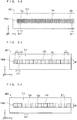
- the second electrode 5 includes the first line-shaped portion 5a as a busbar electrode and a plurality of second line-shaped portions 5b as a finger electrode.
- the first line-shaped portion 5a extends in a Y direction which is a first extending direction.
- Each of the second line-shaped portions 5b extends in an X direction which is a second extending direction (longitudinal direction of the second line-shaped portions 5b) which is different from the first extending direction.
- the first line-shaped portion 5a intersects the plurality of second line-shaped portions 5b.
- the second concentration region 1Hn extends along the boundary between the second semiconductor region In and the second electrode 5.
- the second concentration region 1Hn extends along the second electrode 5.
- the second electrode 5 may include a third line-shaped portion which extends in the Y direction and is connected to the plurality of second line-shaped portions 5b.
- a line width of the first line-shaped portion 5a may be greater than a line width of the plurality of second line-shaped portions 5b. Specifically, it is sufficient that the line width of the second line-shaped portion 5b in the Y direction which is the short direction (line width direction) is approximately equal to or greater than 50 ⁇ m and equal to or less than 200 ⁇ m, for example.
- the line width of the first line-shaped portion 5a in the X direction which is the short direction (line width direction) is approximately equal to or greater than 1.3 mm and equal to or less than 2.5 mm, for example.
- an interval between the adjacent second line-shaped portions 5b among the plurality of second line-shaped portions 5b is approximately equal to or greater than 1.5 mm and equal to or less than 3 mm.
- a thickness of the second electrode 5 is approximately equal to or greater than 10 ⁇ m and equal to or less than 40 ⁇ m, for example.
- the second electrode 5 may include one or more first line-shaped portions 5a, for example.
- the second electrode 5 includes three first line-shaped portions 5a.
- an interval between the adjacent first line-shaped portions 5a among the three first line-shaped portions 5a is approximately 50 mm, for example.
- the second electrode 5 is formed of a similar material and by a similar manufacturing method to that of the above-described output extraction electrode 4b.
- the second electrode 5 is formed by coating the Ag paste to the second main surface 1b of the semiconductor substrate 1 at a predetermined pattern by screen printing or the like, and thereafter by firing the paste.
- the alignment reference portions 1m which are provided at two or more locations in the surface layer portion on the second main surface 1b side of the semiconductor substrate 1 is considered as a reference, and a region (formed region) in which the second electrode 5 is formed is adjusted. Accordingly, the second electrode 5 can be formed on the second concentration region 1Hn of the semiconductor substrate 1 with high accuracy.
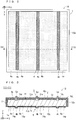
- a solar cell module 100 includes one or more solar cell elements 10.
- the solar cell module 100 includes the plurality of solar cell elements 10 which are electrically connected to each other.
- the solar cell module 100 is formed by connecting the plurality of solar cell elements 10 to each other, for example, in series and in parallel. For example, when the plurality of solar cell modules 100 are combined, a practical electric output can be extracted.
- the solar cell module 100 includes a stacked body in which a transparent member 104, a front side filler 102, a plurality of solar cell elements 10, a wiring member 101, a rear side filler 103, and a rear surface protector 105 are stacked.
- the transparent member 104 is a member for protecting the light receiving surface in the solar cell module 100.
- the transparent member 104 is a transparent flat plate-shaped member.
- As a material of the transparent member 104 for example, glass or the like is employed.
- the front side filler 102 and the rear side filler 103 may be, for example, transparent fillers.
- the rear surface protector 105 is a member for protecting the solar cell module 100 from the rear surface.
- a material of the rear surface protector 105 for example, polyethylene terephthalate (PET), polyvinyl fluoride resin (PVE) or the like is employed.
- PET polyethylene terephthalate
- PVE polyvinyl fluoride resin
- the rear surface protector 105 may have a mono-layered structure or a stacked structure.
- the wiring member 101 is a member (connection member) which electrically connects the plurality of solar cell elements 10 to each other. Between the solar cell elements 10 adjacent in a ⁇ Y direction in the plurality of solar cell elements 10 which are included in the solar cell modules 100, the first electrode 4 in one solar cell element 10 and the second electrode 5 in the other solar cell element 10 are connected to each other by the wiring member 101. Accordingly, the plurality of solar cell elements 10 are electrically connected to each other in series.
- a thickness of the wiring member 101 may be approximately equal to or greater than 0.1 mm and equal to or less than 0.2 mm, for example. It is sufficient that a width of the wiring member 101 is approximately 2 mm.
- the wiring member 101 for example, a member of which the entire surface of copper foil is covered by soldering is employed.
- each of one end of the electrode of a first solar cell element 10 and one end of the electrode of a last solar cell element 10 is electrically connected to a terminal box 107 as the output extraction portion, by an output extraction wiring 106.
- the solar cell module 100 may include a frame 108 which holds the above-described stacked body at the periphery.
- a material of the frame 108 for example, Al or the like which has both corrosion resistance and intensity is employed.
- the EVA When the EVA is employed as a material of at least one of the front side filler 102 and the rear side filler 103, since the EVA includes a vinyl acetate, an acetate tends to be generated due to sequential hydrolysis because the EVA transmits moisture or water when the temperature is high. In contrast, when an acid acceptor including a magnesium hydroxide or a calcium hydroxide is added to the EVA, generation of the acetate from the EVA can be reduced. Accordingly, corrosion resistance of the solar cell module 100 can be improved. In other words, it is possible to ensure reliability of the solar cell module 100 for a long period of time.
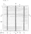
- the second semiconductor region In is provided across the entire region of the surface layer portion on the second main surface 1b side in the semiconductor substrate 1.
- the first concentration region 1Ln is placed, and the second concentration region 1Hn extends.
- the second concentration region 1Hn includes a first line-shaped region 1Hna and a plurality of second line-shaped regions 1Hnb.
- the first line-shaped region 1Hna extends in the Y direction which is the first extending direction.
- Each of the second line-shaped regions 1Hnb extends in the X direction which is the second extending direction.
- the first line-shaped region 1Hna intersects the plurality of second line-shaped regions 1Hnb.
- a third line-shaped region which extends in the Y direction and is connected to the plurality of second line-shaped regions 1Hnb maybe included.
- a width of the first line-shaped region 1Hna is greater than a width of the plurality of second line-shaped regions 1Hnb.
- a line width of the second line-shaped region 1Hnb in the Y direction which is the short direction (line width direction) is approximately equal to or greater than 100 ⁇ m and equal to or less than 500 ⁇ m, for example.
- a width of the first line-shaped region 1Hna in the X direction which is the short direction (line width direction) is approximately equal to or greater than 2.5 mm and equal to or less than 5 mm, for example.
- an interval between the adjacent second line-shaped regions 1Hnb among the plurality of second line-shaped regions 1Hnb is approximately equal to or greater than 1.5 mm and equal to or less than 3 mm.
- a thickness of the second semiconductor region In is approximately equal to or greater than 0.5 ⁇ m and equal to or less than 2 ⁇ m.
- the second semiconductor region In includes one or more first line-shaped regions 1Hna.
- the second semiconductor region In includes three first line-shaped regions 1Hna. It is sufficient that an interval between the adjacent first line-shaped regions 1Hna among the three first line-shaped regions 1Hna is approximately 50 mm, for example.
- the second electrode 5 is placed on the second concentration region 1Hn. Specifically, the first line-shaped portion 5a is placed on each of the first line-shaped regions 1Hna of the second concentration region 1Hn. In addition, the second line-shaped portions 5b are placed on the respective second line-shaped regions 1Hnb of the second concentration region 1Hn.
- the n-type dopant concentration as the second conductivity type in the first concentration region 1Ln is in the first concentration range.
- the n-type dopant concentration in the entire second concentration region 1Hn is higher than the n-type dopant concentration in the entire first concentration region 1Ln.
- the second concentration region 1Hn includes a region (high concentration region) in which the n-type dopant concentration as the second conductivity type is in the second concentration range.
- the second concentration region 1Hn includes a plurality of high concentration regions which are arranged in the extending direction of the second concentration region 1Hn.
- the first line-shaped region 1Hna includes the plurality of high concentration regions which are arranged in the Y direction which is the first extending direction.
- the second line-shaped region 1Hnb includes the plurality of high concentration regions which are arranged in the X direction which is the second extending direction.
- each high concentration region is formed by irradiating a supply source with the laser light in a state where the supply source of the n-type dopant is placed on the first concentration region 1Ln.
- a thickness and the extending direction of the first line-shaped region 1Hna and the second line-shaped region 1Hnb are different from each other, but the configuration is similar to each other.
- a configuration of the second line-shaped region 1Hnb will be described as an example.
- the second line-shaped region 1Hnb includes a plurality of high concentration regions 1Hr which are provided in the X direction which is the longitudinal direction thereof.
- a frequency of occurrence of the plurality of high concentration regions 1Hr in the X direction which is the second extending direction is appropriately set. Accordingly, the local n-type dopant concentration in the second line-shaped region 1Hnb can be appropriately set.
- the first concentration region 1Ln exists at a position which is apart from the second line-shaped portions 5b by a predetermined distance in plan view.
- a length (overlapped length) Ls1 in the X direction of a region (overlapped region) 1Sc in which two or more high concentration regions 1Hr are overlapped with each other, and a distance (separation distance) Ds1 in the X direction between two high concentration regions 1Hr, are appropriately set. Accordingly, the local n-type dopant concentration in the second line-shaped region 1Hnb can be set.
- the non-arrangement region 1Sa corresponds to the gap between two adjacent high concentration regions 1Hr.
- a shape and a size of the high concentration region 1Hr are determined by a shape, a size, a positional tolerance, a width tolerance of the second electrode 5, and irradiation positional tolerance and a width tolerance of the laser light.
- a line width W2 of the second line-shaped portions 5b in the Y direction which is the line width direction is approximately 100 ⁇ m
- a sum of the irradiation positional tolerance and the width tolerance of the laser light is ⁇ 80 ⁇ m.
- a line width W1 of the second line-shaped region 1Hnb in the Y direction which is the line width direction and the width W1 of the high concentration regions 1Hr in the Y direction is approximately 260 ⁇ m.
- a length L1 of the high concentration regions 1Hr in the X direction is set to be approximately 200 ⁇ m, the overlapped region 1Sc and the separation distance Ds1 are easily set, and the second line-shaped portions 5b can be located on the second line-shaped regions 1Hnb with high accuracy.
- a distance Lo1 from an end portion of the semiconductor substrate 1 to an end portion of the second line-shaped portions 5b is set to be approximately 1.5 mm, for example.
- the first concentration region 1Ln When forming the first concentration region 1Ln, at least one of a concentration of elements which become dopant supplied to the second main surface 1b of the semiconductor substrate 1 and a temperature of the semiconductor substrate 1 may vary. Accordingly, dopant concentration in the first concentration region 1Ln may vary. As a result, sheet resistance ps in the first concentration region 1Ln may vary.
- the first concentration region 1Ln when forming the first concentration region 1Ln, it is assumed that raw material gas having a lower temperature than the temperature of the semiconductor substrate 1 is supplied from the one end portion side of the semiconductor substrate 1.
- the raw material gas is gas containing an element which becomes the n-type dopant.
- the temperature on the one end portion side of the semiconductor substrate 1 can be lower than the temperature of a center portion of the semiconductor substrate 1.
- the element which becomes the dopant is unlikely to be introduced by diffusion.
- the n-type dopant concentration in the first concentration region 1Ln which is positioned on the one end portion side of the semiconductor substrate 1 is lower than the n-type dopant concentration in the first concentration region 1Ln which is positioned in the center portion of the semiconductor substrate 1.
- the sheet resistance ps in the first concentration region 1Ln which is positioned on the one end portion side of the semiconductor substrate 1 is higher than the sheet resistance ps in the first concentration region 1Ln which is positioned in the center portion of the semiconductor substrate 1.
- the raw material gas flows from the one end portion side of the semiconductor substrate 1 toward the other end portion side, in the heating furnace.
- a concentration gradient of the raw material gas can be generated from an upside of the one end portion to an upside of the other end portion of the semiconductor substrate 1.
- the n-type dopant concentration in the first concentration region 1Ln shows a tendency of decreasing from the one end portion to the other end portion of the semiconductor substrate 1.
- the sheet resistance ps in the first concentration region 1Ln shows a tendency of increasing from the one end portion to the other end portion of the semiconductor substrate 1.
- the first concentration region 1Ln When forming the first concentration region 1Ln, it is considered that there is a case in which the raw material gas having a lower temperature than the temperature of the semiconductor substrate 1 is supplied, but a temperature distribution depending on a supply direction of the raw material gas is not generated in the semiconductor substrate 1. In this case, according to a cooling effect by the flow of the raw material gas, the temperature of the end portion of the entire periphery of the semiconductor substrate 1 can be lower than the temperature of the center portion of the semiconductor substrate 1. Accordingly, in the end portion of the entire periphery of the semiconductor substrate 1 rather than the center portion of the semiconductor substrate 1, the element which becomes the dopant is unlikely to be introduced by diffusion.
- the n-type dopant concentration in the first concentration region 1Ln is lower in the end portion of the entire periphery of the semiconductor substrate 1 than that in the center portion of the semiconductor substrate 1.
- the sheet resistance ps in the first concentration region 1Ln in the end portion of the entire periphery of the semiconductor substrate 1 is higher than that in the center portion of the semiconductor substrate 1.
- the sheet resistance ps in the first concentration region 1Ln and the second concentration region 1Hn is measured by a four-probe method, in a darkroom which has 25.5°C of room temperature, and 60%RH of relative humidity, for example.
- the four-probe method is a four-probe method based on JIS H 0602-1995 (resistivity measuring method by the four-probe method of silicon monocrystal and silicon wafer).
- the sheet resistance ps for example, a sheet resistance which is corrected to a value under a condition of 25°C of room temperature from a value obtained at 25.5°C is employed.
- Measurement of the sheet resistance ps in the first concentration region 1Ln and the sheet resistance ps in the second concentration region 1Hn is performed after forming the second semiconductor region In by introducing the n-type dopant into the surface layer portion on the second main surface 1b side in the semiconductor substrate 1 by diffusion.
- each sheet resistance ps can be measured by allowing the probe to be in contact from above a thin film of the supply source (element supply source) of the dopant formed on the second main surface 1b.
- the element supply source for example, a phosphosilicate glass layer (PSG layer) or the like is employed.
- the semiconductor substrate 1 is removed from the heating furnace for forming the first concentration region 1Ln, the semiconductor substrate 1 is left for approximately 20 minutes in the darkroom, and the temperature of the semiconductor substrate 1 becomes substantially equal to the room temperature. Subsequently, for example, after the semiconductor substrate 1 is disposed in a measurement instrument, static electricity is removed from the surface of the semiconductor substrate 1 by grounding.
- the distance between the probes is set to be approximately 1 mm, for example.
- a diameter of a tip end of the probe is set to be approximately 100 ⁇ m, for example.
- tungsten carbide As a material of the surface of the probe, for example, tungsten carbide is employed.
- a weight for pressing the probe to the semiconductor substrate 1 is set to be 1 N, for example.
- a current applied between the probes is set to be 1 mA, for example.
- a measurement value is read in 1 second after the current is started to be applied.
- an average of 10 measurement values at the same measurement position is calculated as the sheet resistance ps.
- a line width in the second concentration region 1Hn is narrow. Accordingly, when measuring the sheet resistance ps in the second concentration region 1Hn, the distance between the probes is set to be approximately 0.1 mm, for example. The diameter of the tip end of the probe is set to be 10 ⁇ m, for example. As the material of the surface of the probe, tungsten carbide is employed. The weight for pressing the probe to the semiconductor substrate 1 is set to be 0.1 N, for example. The current applied between the probes is set to be 0.1 mA, for example. For example, the measurement value is read in 1 second after the current is started to be applied. For example, an average of 10 measurement values at the same measurement position is calculated as the sheet resistance ps.
- Formula (1) is a general formula which expresses the volume resistivity p.
- Formula (2) holds true when the volume resistivity p of a layer (diffusion layer) which is formed by introducing the n-type dopant into the surface layer portion of the semiconductor substrate 1 by diffusion is uniform and a depth of this diffusion layer is t. In the embodiment, the depth t may be 2 ⁇ m.
- the sheet resistance ps can be calculated.
- the thickness and the size of the semiconductor substrate 1 are not sufficient; the width, the length, and the depth in the first concentration region 1Ln and the second concentration region 1Hn as the diffusion layer are not sufficient; and the measurement position is positioned in the vicinity of the end portion of the semiconductor substrate 1.
- the measurement value of the sheet resistance ps which is calculated by Formula (1) and Formula (2), an error from a true value is generated.
- the sheet resistance ps of the second semiconductor region In is lower than the sheet resistance ps of the first semiconductor region 1p.
- the measurement value of the sheet resistance ps in the first concentration region 1Ln can be measured as a value which is slightly higher than the true value.
- the sheet resistance ps in the second concentration region 1Hn is lower than the sheet resistance ps in the first concentration region 1Ln. Accordingly, because the width and the length of the second concentration region 1Hn are limited, a measurement value of the sheet resistance ps in the second concentration region 1Hn can be measured as a value which is slightly higher than the true value.
- the error is relatively small, a correction for reducing the error from the true value caused by the size and the shape of each region may not be performed.
- a measuring method of the sheet resistance ps in the first concentration region 1Ln and the second concentration region 1Hn for example, a measuring method in which a secondary ion mass spectrometry method (SIMS) is employed.
- SIMS secondary ion mass spectrometry method
- the thin film (PSG layer or the like) of the element supply source formed on the second main surface 1b is removed by cleaning using a hydrofluoric acid (HF) or the like
- HF hydrofluoric acid
- a donor concentration Nd and an acceptor concentration Na in the first concentration region 1Ln and the second concentration region 1Hn are measured by the SIMS.
- each of the volume resistivity p in the first concentration region 1Ln and the second concentration region 1Hn is calculated.
- the volume resistivity p is substituted in Formula (2), the sheet resistance ps in the first concentration region 1Ln and the sheet resistance ps in the second concentration region 1Hn are respectively calculated.
- the sheet resistance ps According to the measuring method of the sheet resistance ps, a part of the measurement target region is destroyed. However, the sheet resistance ps can be calculated from the analysis result of the donor concentration and the acceptor concentration in the extremely small measurement target region. Accordingly, regarding the measurement value of the sheet resistance ps obtained by the measuring method, the error from the true value caused by the size, the shape and the like of the first concentration region 1Ln and the second concentration region 1Hn can be small.
- the n-type dopant concentration in the first concentration region 1Ln and the second concentration region 1Hn can be measured by, for example, time-of-flight secondary ion mass spectrometry (TOF-SIMS) in which each surface of the first concentration region 1Ln and the second concentration region 1Hn is considered as the measurement target region.
- TOF-SIMS time-of-flight secondary ion mass spectrometry
- concentration distribution of P which is the n-type dopant is visibly output, the position of the high concentration region 1Hr and a two-dimensional distribution of the n-type dopant concentration can be confirmed.
- the frequency of occurrence of the plurality of high concentration regions 1Hr in the second concentration region 1Hn in the extending direction is appropriately adjusted. Accordingly, the n-type dopant concentration and the sheet resistance ps in the second concentration region 1Hn are adjusted. As a result, the distribution of the sheet resistance ps in the second concentration region 1Hn can be narrow and can be settled in an appropriate value range.
- the n-type dopant concentration and the sheet resistance are different.
- an outer edge of the close region 1NA is illustrated by a dotted line.
- the close region 1NA is a region which is close to the second line-shaped region 1Hnb in a direction (intersection direction) which intersects the second extending direction of the second line-shaped region 1Hnb in the first concentration region 1Ln.
- the close region 1NA is a region which is included in a range of a preset distance from the second line-shaped region 1Hnb.
- the preset distance may be equal to or less than the interval between adjacent second line-shaped regions 1Hnb, for example. It is sufficient that the interval between the adjacent second line-shaped regions 1Hnb is approximately equal to or greater than 1 mm and equal to or less than 2 mm, for example. Accordingly, the above-described preset distance may be approximately equal to or greater than 100 ⁇ m and equal to or less than 1000 ⁇ m, for example.
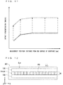
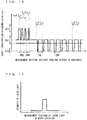
- a distribution of the sheet resistance ps in the X direction in the close region 1NA is illustrated by a bold line.
- a distribution of the sheet resistance ps in the X direction in the second line-shaped region 1Hnb is illustrated by a bold line.
- a distance from an end surface on the -X side of the semiconductor substrate 1 to the measurement position is illustrated, and on a vertical axis, the sheet resistance ps is illustrated.
- the sheet resistance ps in the close region 1NA shows a tendency of increasing as approaching the one end portion side (-X side) of the semiconductor substrate 1 and decreasing as approaching the center portion side of the semiconductor substrate 1, in the X direction.
- the sheet resistance ps in the close region 1NA is included in a value range Rr1.
- the n-type dopant concentration in the close region 1NA shows a tendency of decreasing as approaching the one end portion side (-X side) of the semiconductor substrate 1 and increasing as approaching the center portion side of the semiconductor substrate 1, in the X direction.
- the second line-shaped region 1Hnb is replaced with a second line-shaped region 1HnbA in which the frequency of occurrence of the plurality of high concentration regions 1Hr is set to be constant in the X direction (reference example).
- the n-type dopant concentration in the second line-shaped region 1HnbA increases with substantially the same tendency as that of the concentration distribution of the close region 1NA.
- a distribution of the sheet resistance ps in the X direction in the second line-shaped region 1HnbA according to the reference example is illustrated by a bold dotted line.
- the sheet resistance ps in the second line-shaped region 1HnbA is included in a value range Rr2A.
- the frequency of occurrence of the plurality of high concentration regions 1Hr in the X direction is adjusted. Accordingly, the n-type dopant concentration and the sheet resistance ps in the second line-shaped region 1Hnb are adjusted, and as illustrated by the bold line in Fig. 10 , the sheet resistance ps in the second line-shaped region 1Hnb can be settled in the appropriate value range Rr2 which is narrower than the value range Rr2.
- the dopant concentration difference is a difference which can be obtained by subtracting the n-type dopant concentration in the close region 1NA from the n-type dopant concentration in the second line-shaped region 1Hnb.
- a length in the X direction which is the second extending direction in the measurement target region may be approximately equal to or greater than 0.01 mm and equal to or less than 0.1 mm, for example.
- a distance from the end surface on the -X side of the semiconductor substrate 1 to the measurement position is illustrated on a horizontal axis, and the dopant concentration difference is illustrated on a vertical axis.
- an example of the distribution of the dopant concentration difference regarding the second line-shaped region 1HnbA according to the reference example illustrated in Fig. 12 is illustrated by a bold broken line.
- the dopant concentration difference repeatedly increases or decreases in the X direction which is the second extending direction of the second line-shaped region 1Hnb.
- the dopant concentration difference repeatedly increases or decreases between a value range Dd0 of roughly zero as a first value range and a value range Dd1 as a second value range in the X direction.
- the value range Dd1 is a value range within a range of ⁇ 30% of a reference value having the preset reference value as a center.
- the value range Dd1 is a range which is equal to or greater than 0.7 ⁇ 10 20 atoms/cm 3 and equal to or less than 1.3 ⁇ 10 20 atoms/cm 3 .
- the dopant concentration difference is repeatedly increasing or decreasing between the value range Dd1 which is the first value range and a value range Dd2 which is a second value range in the X direction.
- the value range Dd2 is a value range within a range of ⁇ 30% of the reference values having the preset reference value as the center.
- the value range Dd2 is a range which is equal to or greater than 1.4 ⁇ 10 20 atoms/cm 3 and equal to or less than 2.6 ⁇ 10 20 atoms/cm 3 .
- a specific example of a range regarding the above-described value ranges Dd1 and Dd2 is merely an example, and the value ranges Dd1 and Dd2 are not limited to the above-described ranges.
- the value range Dd1 and the value range Dd2 may be different according to the position.
- each of the value range Dd1 and the value range Dd2 may not be a constant value range in the entire second concentration region 1Hn.
- the region of the preset size may be a region which has 10 millimeters square, for example. More specifically, for example, in the preset region of the second semiconductor region In, a relationship between the value range Dd1 and the value range Dd2 in which a value which is obtained by dividing the value range Dd2 by the value range Dd1 is equal to or greater than 1.5 and equal to or less than 3, can be considered.
- the dopant concentration difference is maintained to be substantially constant in the X direction which is the extending direction of the second line-shaped region 1HnbA.
- an occupancy rate of a section in which the dopant concentration difference is included in the second value range among sections of a unit length L 0 increases.
- the occupancy rate of the section in which the dopant concentration difference is included in the value range Dd1 serving as the second value range among the sections of the unit length L 0 increases, as moving to the -X side.
- the occupancy rate of a section in which the dopant concentration difference is included in the value range Dd2 serving as the second value range among the sections of the unit length L 0 increases. Accordingly, the dopant concentration in the second line-shaped region 1Hnb which is formed by using a part having a relatively low dopant concentration in the first concentration region 1Ln as a base portion can appropriately increase. As a result, the distribution of the sheet resistance ps in the second line-shaped region 1Hnb can be narrow and can be settled in an appropriate value range.
- the unit length L 0 is longer than a length L1 in the X direction of the high concentration regions 1Hr, and for example, the unit length L 0 can be set to be equal to or greater than 1.1 times and equal to or less than several times of the length L1. For example, when the length L1 is approximately 200 ⁇ m, the unit length L 0 is set to be approximately 280 ⁇ m.
- Fig. 13 sections from L 0 1 to L 0 4 having the unit length L 0 are illustrated. The sections from L 0 1 to L 0 4 are provided in this order toward the end portion of the -X side from the center portion of the semiconductor substrate 1.
- the occupancy rate of the section in which the dopant concentration difference is included in the value range Dd1 serving as the second value range in the section L 0 2 is greater than the occupancy rate of the section in which the dopant concentration difference is included in the value range Dd1 serving as the second value range in the section L 0 1.
- the occupancy rate of the section in which the dopant concentration difference is included in the value range Dd1 serving as the second value range among the sections of the unit length L 0 increases.
- the occupancy rate of the section in which the dopant concentration difference is included in the value range Dd1 serving as the second value range among the sections of the unit length L 0 can easily increase.
- the plurality of high concentration regions 1Hr include a single arrangement region 1Sb as the first high concentration region and an overlapped region 1Sc as the second high concentration region.
- the dopant concentration difference regarding the single arrangement region 1Sb is included in the value range Dd1 serving as the first value range.
- the dopant concentration difference in the overlapped region 1Sc is included in the value range Dd2 serving as the second value range which is larger than the value range Dd1.
- the single arrangement region 1Sb having the dopant concentration difference of the value range Dd1 and the overlapped region 1Sc having the dopant concentration difference of the value range Dd2 repeatedly exist.
- the occupancy rate of the section in which the dopant concentration difference is included in the value range Dd2 serving as the second value range in the section L 0 4 is greater than the occupancy rate of the section in which the dopant concentration difference is included in the value range Dd2 serving as the second value range in the section L 0 3.
- the occupancy rate of the section in which the dopant concentration difference is included in the value range Dd2 serving as the second value range among the sections of the unit length L 0 increases.
- the occupancy rate of the section in which the dopant concentration difference is included in the value range Dd2 serving as the second value range among the sections of the unit length L 0 can easily increase.
- the occupancy rate of the section in which the dopant concentration difference is included in the second value range among the sections of the unit length L 0 is greater on the one end portion side (-X side) than that on the center portion side in the X direction which is the second extending direction of the second line-shaped region 1Hnb.
- a state where the occupancy rate increases as moving to the -X side is illustrated.
- the n-type dopant concentration in the second line-shaped region 1Hnb can further increase.
- the distribution of the dopant concentration in the second line-shaped region 1Hnb can be narrow and can be settled in a high value range. Therefore, the distribution of the sheet resistance ps in the second line-shaped region 1Hnb can be narrow and can be settled in an appropriate value range.
- Fig. 15 when laser light having a non-top-hat type intensity distribution illustrated in Fig. 16 is used, an example of a detailed distribution of the dopant concentration difference regarding the second line-shaped region 1Hnb is illustrated by a bold line.
- the detailed distribution of the dopant concentration difference can be obtained when the measurement target region of the dopant concentration is set to be narrow.
- Fig. 15 similarly to Fig. 13 , the distance from the end surface on the -X side to the measurement position of the semiconductor substrate 1 is illustrated on a horizontal axis, and the dopant concentration difference is illustrated on a vertical axis.
- a change in the dopant concentration difference is focused which is obtained by subtracting the dopant concentration value at a place which is close to a one place in the first concentration region 1Ln from the dopant concentration value at the one place in the second line-shaped region 1Hnb.
- the one place and the place which is close to the one place may be close to each other in the Y direction.
- the place which is close to the one place may be included in the close region 1NA, for example.
- the minimum place which has the minimum value of the dopant concentration difference and the maximum place which has the maximum value of the dopant concentration difference alternately and repeatedly exist.
- a part in which an interval (minimum place interval) IN1 between one end portions of the adjacent minimum places varies exists.
- one end portion of the minimum place is an end portion on the -X side of the minimum place.
- one end portion of the minimum place in the second line-shaped region 1Hnb is a part in which the dopant concentration difference decreases and reaches the minimum place as moving forward from the end surface side of the semiconductor substrate 1 in the -X direction.
- the minimum place interval IN1 appropriately varies, and thereby the second conductivity type dopant concentration in the second line-shaped region 1Hnb is appropriately adjusted. Accordingly, the second conductivity type dopant concentration in the second line-shaped region 1Hnb which is formed by using a part having a relatively low second conductivity type dopant concentration in the first concentration region 1Ln as a base portion can appropriately increase. As a result, the distribution of the sheet resistance ps in the second line-shaped region 1Hnb can be narrow and can be settled in an appropriate value range. Therefore, by improving the boundary part between the semiconductor substrate 1 and the second electrode 5, the conversion efficiency of the solar cell element 10 can be improved.
- the minimum place interval IN1 widens along the second extending direction (X direction).
- the minimum place interval IN1 becomes gradually narrow along a direction (-X direction) which is reverse to the second extending direction (X direction).
- the minimum place interval IN1 becomes gradually narrow. In the vicinity of the center portions from the right portions in Figs.
- a state is illustrated where the plurality of high concentration regions 1Hr are arranged in the second extending direction (X direction), and the minimum place interval IN1 becomes gradually narrow as the separation distance Ds1 between the adjacent high concentration regions 1Hr becomes short along the -X direction.
- a state is illustrated where the minimum place interval IN1 becomes gradually narrow as the overlapped length Ls1 of the high concentration regions 1Hr along the -X direction becomes long.
- the dopant concentration can appropriately increase in the second line-shaped region 1Hnb which is formed by using the part having a relatively low dopant concentration in the first concentration region 1Ln as a base portion.
- the distribution of the sheet resistance ps in the second line-shaped region 1Hnb can be narrow and can be settled in an appropriate value range.
- the minimum place interval IN1 in the one end portion (a part on the -X side) of the second line-shaped region 1Hnb is narrower than the minimum place interval IN1 in the center portion of the second line-shaped region 1Hnb.
- Figs. 13 and 15 in the second extending direction (X direction), a state is illustrated where the minimum place interval IN1 in the one end portion (a part on the -X side) of the second line-shaped region 1Hnb is narrower than the minimum place interval IN1 in the center portion of the second line-shaped region 1Hnb.
- the n-type dopant concentration in the second line-shaped region 1Hnb can appropriately increase.
- the distribution of the dopant concentration in the second line-shaped region 1Hnb can be narrow and can be settled in a high value range. Therefore, the distribution of the sheet resistance ps in the second line-shaped region 1Hnb can be narrow and can be settled in an appropriate value range.
- the difference (sheet resistance difference) of the sheet resistance ps between the second line-shaped region 1Hnb and the close region 1NA which is close to the second line-shaped region 1Hnb in the first concentration region 1Ln changes.
- the sheet resistance difference is a difference which can be obtained by subtracting the sheet resistance in the second line-shaped region 1Hnb from the sheet resistance in the close region 1NA.
- Fig. 17 an example of the detailed distribution of the sheet resistance difference regarding the second line-shaped region 1Hnb is described by a bold line.
- the detailed distribution of the sheet resistance difference can be obtained by setting the measurement target region of the sheet resistance ps to be narrow.
- a method of setting the distance between the probes in the four-probe method to be narrow or a method of setting the measurement target region by the SIMS to be narrow may be employed.
- the length of the second line-shaped region 1Hnb in the X direction which is the second extending direction in the measurement target region is set to be approximately equal to or greater than 0.01 mm and equal to or less than 0.1 mm, for example.
- Fig. 17 an example of the detailed distribution of the sheet resistance difference regarding the second line-shaped region 1Hnb is described by a bold line.
- the detailed distribution of the sheet resistance difference can be obtained by setting the measurement target region of the sheet resistance ps to be narrow.
- the distance from the end surface on the -X side to the measurement position of the semiconductor substrate 1 is illustrated on a horizontal axis, and the sheet resistance difference is illustrated on a vertical axis.
- an example of the distribution of the sheet resistance difference regarding the second line-shaped region 1HnbA according to the reference example illustrated in Fig. 12 is illustrated by the bold dotted line.
- the sheet resistance difference repeats increasing or decreasing in the second extending direction(X direction) of the second line-shaped region 1Hnb.
- the sheet resistance difference repeats increasing or decreasing between a roughly zero value range Dr0 serving as the first value range and a value range Dr1 serving as the second value range in the X direction.
- the value range Dr1 is a value range in a range of ⁇ 20% of the reference value having the preset reference value as a center.
- the value range Dr1 is a range in which the value is equal to or greater than 40 ⁇ / ⁇ and equal to or less than 60 ⁇ / ⁇ .
- the sheet resistance difference repeats increasing or decreasing between the value range Dr1 serving as the first value range and a value range Dr2 serving as the second value range in the X direction.
- the value range Dr2 is a value range within a range of ⁇ 20% of the reference value having the preset reference value as a center.
- the value range Dr2 is a range in which the value is equal to or greater than 64 ⁇ / ⁇ and equal to or less than 96 ⁇ / ⁇ .
- a specific example of the formula range in the above-described value ranges Dr1 and Dr2 are merely an example, and the value ranges Dr1 and Dr2 are not limited to the above-described formula range.
- the value range Dr1 and the value range Dr2 may be different according to the position. In other words, for example, each of the value range Dr1 and the value range Dr2 may not be a constant value range in the entire second concentration region 1Hn.
- the region of the preset size is a region which has 10 millimeters square, for example. More specifically, for example, in the preset region of the second semiconductor region In, an aspect having a relationship between the value range Dr1 and the value range Dr2 in which a value which is obtained by dividing the value range Dr2 by the value range Dr1 is equal to or greater than 1.2 and equal to or less than 2.8, can be considered.
- the sheet resistance difference is maintained to be substantially constant in the X direction which is the extending direction of the second line-shaped region 1HnbA.
- an occupancy rate of a section in which the sheet resistance difference is included in the second value range among the sections of a unit length L 0 increases.
- the occupancy rate of a section in which the sheet resistance difference is included in the value range Dr1 serving as the second value range among the sections of the unit length L 0 increases.
- the occupancy rate of a section in which the sheet resistance difference is included in the value range Dr2 serving as the second value range among the sections of the unit length L 0 increases. Accordingly, the sheet resistance ps can appropriately decrease in the second line-shaped region 1Hnb which is formed by using a part having a relatively high sheet resistance in the first concentration region 1Ln as a base portion. As a result, the distribution of the sheet resistance ps in the second line-shaped region 1Hnb can be narrow and can be settled in an appropriate value range.
- Fig. 17 similarly to Fig. 13 , the sections L 0 1 to L 0 4 having the unit length L 0 are illustrated.
- the sections L 0 1 to L 0 4 are provided in this order toward the end portion of the -X side from the center portion of the semiconductor substrate 1.
- the occupancy rate of the section in which the sheet resistance difference is included in the value range Dr1 serving as the second value range in the section L 0 2 is greater than the occupancy rate of the section in which the sheet resistance difference is included in the value range Dr1 serving as the second value range in the section L 0 1.
- the occupancy rate of the section in which the sheet resistance difference is included in the value range Dr1 serving as the second value range among the sections of the unit length L 0 increases.
- the occupancy rate of the section in which the sheet resistance difference is included in the value range Dr1 serving as the second value range among the sections of the unit length L 0 can easily increase.
- the plurality of high concentration regions 1Hr include the single arrangement region 1Sb as the first high concentration region and the overlapped region 1Sc as the second high concentration region.
- the sheet resistance difference in the single arrangement region 1Sb is included in the value range Dr1 serving as the first value range.
- the sheet resistance difference in the overlapped region 1Sc is included in the value range Dr2 serving as the second value range which is larger than the value range Dr1.
- the single arrangement region 1Sb having the sheet resistance difference of the value range Dr1 and the overlapped region 1Sc having the sheet resistance difference of the value range Dr2 repeatedly exist.
- the occupancy rate of the section in which the sheet resistance difference is included in the value range Dr2 serving as the second value range in the section L 0 4 is greater than the occupancy rate of the section in which the sheet resistance difference is included in the value range Dr2 serving as the second value range in the section L 0 3.
- the occupancy rate of the section in which the sheet resistance difference is included in the value range Dr2 serving as the second value range among the sections of the unit length L 0 increases.
- the occupancy rate of the section in which the sheet resistance difference is included in the value range Dr2 serving as the second value range among the sections of the unit length L 0 can easily increase.
- the occupancy rate of the section in which the sheet resistance difference is included in the second value range among the sections of the unit length L 0 is greater on the one end portion side (-X side) than that on the center portion side in the X direction which is the second extending direction of the second line-shaped region 1Hnb.
- a state where the occupancy rate increases as moving to the -X side is illustrated.
- the sheet resistance ps in the second line-shaped region 1Hnb can further decrease.
- the distribution of the sheet resistance ps in the second line-shaped region 1Hnb can be narrow and can be settled in an appropriate value range.
- FIG. 18 an example of the detailed distribution of the sheet resistance difference regarding the second line-shaped region 1Hnb when laser light having a non-top-hat type intensity distribution illustrated in Fig. 16 is used, is illustrated by a bold line.
- the detailed distribution of the sheet resistance difference can be obtained by setting the measurement target region of the sheet resistance ps to be narrow.
- Fig. 18 similarly to Fig. 17 , the distance from the end surface on the -X side to the measurement position of the semiconductor substrate 1 is illustrated on a horizontal axis, and the sheet resistance difference is illustrated on a vertical axis.
- a change in the sheet resistance difference which is obtained by subtracting the sheet resistance ps value at a one place in the second line-shaped region 1Hnb from the sheet resistance ps value at a place which is close to the one place in the first concentration region 1Ln, is focused.
- the one place and the place which is close to the one place may be close to each other in the Y direction. It is sufficient that the place which is close to the one place is included in the close region 1NA, for example.
- the minimum place which has the minimum value of the sheet resistance difference and the maximum place which has the maximum value of the sheet resistance difference alternately and repeatedly exist.
- one end portion of the minimum place is an end portion on the -X side of the minimum place.
- one end portion of the minimum place in the second line-shaped region 1Hnb is a part in which the sheet resistance difference decreases as moving forward from the end surface side of the semiconductor substrate 1 in the -X direction and reaches the minimum place.
- the sheet resistance ps in the close region 1NA which is close to the second line-shaped region 1Hnb can be appropriately adjusted. Accordingly, the second conductivity type sheet resistance ps in the second line-shaped region 1Hnb which is formed by using a part having a relatively high second conductivity type sheet resistance ps in the first concentration region 1Ln as a base portion can appropriately decrease. As a result, the distribution of the sheet resistance ps in the second line-shaped region 1Hnb can be narrow and can be settled in an appropriate value range. Therefore, by improving the boundary part between the semiconductor substrate 1 and the second electrode 5, the conversion efficiency of the solar cell element 10 can be improved.
- the minimum place interval IN2 widens along the second extending direction (X direction).
- the minimum place interval IN2 becomes gradually narrow along a direction (-X direction) which is reverse to the second extending direction (X direction) according to the decrease of the dopant concentration in the close region 1NA.
- the minimum place interval IN2 becomes gradually narrow. In the vicinity of the center portions from the right portions in Figs.
- a state is illustrated where the plurality of high concentration regions 1Hr are arranged in the second extending direction (X direction), and the minimum place interval IN2 becomes gradually narrow as the separation distance Ds1 between the adjacent high concentration regions 1Hr becomes short along the -X direction.
- a state is illustrated where the minimum place interval IN2 becomes gradually narrow as the overlapped length Ls1 of the high concentration region 1Hr becomes long along the -X direction.
- the sheet resistance ps can appropriately decrease in the second line-shaped region 1Hnb which is formed by using the part having a relatively high sheet resistance ps in the first concentration region 1Ln as a base portion.
- the distribution of the sheet resistance ps in the second line-shaped region 1Hnb can be narrow and can be settled in an appropriate value range.
- the minimum place interval IN2 in the one end portion (a part on the -X side) of the second line-shaped region 1Hnb is narrower than the minimum place interval IN2 in the center portion of the second line-shaped region 1Hnb.
- a state is illustrated where the minimum place interval IN2 in the one end portion (a part on the -X side) of the second line-shaped region 1Hnb is narrower than the minimum place interval IN2 in the center portion of the second line-shaped region 1Hnb in the second extending direction (X direction).
- the sheet resistance ps in the second line-shaped regions 1Hnb can appropriately decrease.
- the distribution of the sheet resistance ps in the second line-shaped region 1Hnb can be narrow and can be settled in an appropriate value range.
- the second concentration region is formed by the laser radiation, not only the dopant concentration and the sheet resistance value, but also a fine shape of the surface of the irradiation location is different from those of the other regions. Accordingly, for example, it is possible to distinguish both regions by the colors of the surface of elements which are different from each other when observing by an optical microscope.
- optical current mapping measurement which uses methods, such as an electron beam induced current (EBIC) method or a laser beam induced current (LBIC) method.
- a process (preparation process) of preparing the semiconductor substrate 1 (refer to Fig. 20 ) is performed.
- the p-type semiconductor substrate 1 as the first conductivity type is prepared.
- the semiconductor substrate 1 is a monocrystal silicon substrate, for example, the semiconductor substrate 1 is formed by using a floating zone (FZ) method or the like.
- the semiconductor substrate 1 is a polycrystal silicon substrate, for example, the semiconductor substrate 1 is formed by using a casting method or the like. In this case, for example, first, an ingot of the polycrystal silicon as a semiconductor material is made by the casting method.
- the semiconductor substrate 1 is formed.
- the semiconductor substrate 1 has a rectangular plate surface having 156 mm on one side.
- the semiconductor substrate 1 is a p-type conductivity type by B doping. It is sufficient that specific resistance of the semiconductor substrate 1 is equal to or greater than 1 ⁇ cm and equal to or less than 2 ⁇ cm.
- a process (preprocessing process) of removing a damaged layer from the surface of the semiconductor substrate 1 is performed.
- the damaged layer is a layer which has a mechanical damage and contamination which are caused on a sliced surface of the semiconductor substrate 1 when the semiconductor substrate 1 is thinly sliced in the step S1.
- the damaged layer is removed by performing an extremely small amount of etching by an alkaline or acid solution.
- an alkaline solution for example, an aqueous solution, such as NaOH or KOH, may be employed.
- an aqueous solution such as the HF or a fluonitric acid, may be employed.
- a process (texture processing process) of forming the projection and recess portion 1bL (refer to Fig. 21 ) on the second main surface 1b is performed.
- etching processing is performed by an acid aqueous solution at least on the second main surface 1b in the semiconductor substrate 1, the projection and recess portion 1bL is formed.
- the etching processing for example, wet etching which uses the alkaline solution, such as NaOH or the acid solution, such as the fluonitric acid, or dry etching which uses the RIE or the like, can be employed.
- a process (first forming process) of forming the n-type first concentration region 1Ln (refer to Fig. 22 ) as the second conductivity type in the surface layer portion on the second main surface 1b side which is the one main surface in the semiconductor substrate 1 is performed.
- the first concentration region 1Ln in which the n-type dopant concentration is in the first concentration range is formed by introducing the element which becomes the n-type dopant into the surface layer portion on the second main surface 1b side in the semiconductor substrate 1 by diffusion. It is sufficient that the dopant concentration of the first concentration region may be approximately from 1 ⁇ 10 18 atm/cm 3 to 1 ⁇ 10 20 atm/cm 3 , for example.
- a layer-shaped element supply source GL1 (refer to Fig. 22 ) including the element which becomes the n-type dopant is formed on the first concentration region 1Ln.
- the element supply source GL1 serves as a supply source of the element which becomes the n-type dopant.
- the semiconductor substrate 1 is disposed in a heating furnace 20.
- the heating furnace 20 in the atmosphere of the raw material gas including the element (for example, P) which becomes the n-type dopant, a heat treatment is performed on the semiconductor substrate 1.
- the first concentration region 1Ln is formed by introducing the element, which becomes the n-type dopant, included in the raw material gas into the surface layer portion on the second main surface 1b side of the semiconductor substrate 1 by diffusion. It is sufficient that a thickness of the first concentration region 1Ln is approximately equal to or greater than 0.1 ⁇ m and equal to or less than 1 ⁇ m, for example.
- the heating furnace 20 is provided with a pipe (quartz pipe) 20T made of quartz and a heater 20H which is placed in the periphery of a quartz pipe 20T.
- a gas supply path 20Cs which supplies raw material gas Ga1 to the inside of the quartz pipe 20T, and a gas discharge path 20Ep which discharges gas Ga2 from the inside of the quartz pipe 20T, are provided.
- the raw material gas Ga1 is a gas which contains the element which becomes the n-type dopant of the second conductivity type.
- a cassette made of quartz in which 10 or more and 1000 or less semiconductor substrates 1 are disposed is attached to the inside of the quartz pipe 20T. After a lid of the quartz pipe 20T is closed, the heat treatment is performed with respect to each semiconductor substrate 1. It is sufficient that a temperature raising rate in the heat treatment is equal to or greater than 1°C/minute and 100°C/minute, for example. However, if the temperature raising rate is equal to or greater than 20°C/minute and equal to or less than 50°C/minute, it is possible to shorten the time required for the heat treatment and stabilize the temperature raising. In addition, at this time, it is sufficient that the semiconductor substrate 1 is heated within a range from 300°C to 900°C.
- the time required for the heat treatment can be shortened.
- the temperature of the semiconductor substrate 1 can be uniform.
- the first predetermined time may be equal to or greater than 1 minute and equal to or less than 20 minutes, for example.
- the semiconductor substrate 1 is maintained for a second predetermined time within the temperature range after raising the temperature, O 2 gas and N 2 gas are used as carrier gas, and POCl 3 gas is introduced into the quartz pipe 20T as the raw material gas Ga1 at equal to or greater than 1 sccm and 10000 sccm of flux.
- the second predetermined time may be equal to or greater than 1 minute and equal to or less than 200 minutes, for example.
- the PSG layer as the element supply source GL1 is formed on the surface of the semiconductor substrate 1, and P is introduced into the surface layer portion of the semiconductor substrate 1 by diffusion.
- gas is stopped to be supplied to the inside of the quartz pipe 20T, and the semiconductor substrate 1 is maintained for 1 or more minutes and 200 or less minutes within a predetermined maintaining temperature range. It is sufficient that the predetermined maintaining temperature range is from 800°C to 950°C.
- P is further introduced into the surface layer portion of the semiconductor substrate 1 by diffusion.
- the semiconductor substrate 1 is cooled down to a room temperature at a temperature dropping rate which is equal to or greater than 1°C/minute and equal to or less than 50°C/minute.
- the cassette is extracted from the inside of the quartz pipe 20T, and the semiconductor substrate 1 is further extracted from the cassette.
- the first concentration region 1Ln can be formed in the surface layer portion on the second main surface 1b side of the semiconductor substrate 1.
- the raw material gas Ga1 is supplied to the inside of the heating furnace 20 in a state where the temperature is lower than the temperature of the semiconductor substrate 1 and thereby the first concentration region 1Ln is formed.
- the raw material gas Ga1 is supplied from the one end portion 1Ep side (-X side) of the semiconductor substrate 1. Accordingly, the n-type dopant concentration in the first concentration region 1Ln becomes lower on the one end portion 1Ep side than on a center portion 1Cp side of the semiconductor substrate 1.
- the sheet resistance ps in the first concentration region 1Ln becomes higher on the one end portion 1Ep side (-X side) than on the center portion 1Cp side.
- the semiconductor substrate 1 is heated up to the temperature range of approximately 800°C, for example, by radiant heat from the heater 20H. Meanwhile, the POCl 3 gas is heated only up to a sufficient temperature (for example, approximately 40°C) to be evaporated. Accordingly, compared to the temperature of the semiconductor substrate 1, the temperature of the POCl 3 gas is extremely low. Therefore, by the POCl 3 gas which is supplied to the inside of the quartz pipe 20T, the semiconductor substrate 1 is cooled, and forming the PSG layer on the surface of the semiconductor substrate 1 and diffusion of P to the surface layer portion of the semiconductor substrate 1 are interrupted.
- the PSG layer formed on the second main surface 1b of the semiconductor substrate 1 becomes thin and the sheet resistance ps becomes high in the first concentration region 1Ln.
- a phenomenon that the sheet resistance ps becomes high in the first concentration region 1Ln can be caused in a region approximately from 1 mm to 50 mm from the one end portion 1Ep of the semiconductor substrate 1.
- the sheet resistance ps shows a tendency of increasing in the first concentration region 1Ln.
- the sheet resistance ps in the first concentration region 1Ln is equal to or greater than 60 ⁇ / ⁇ and equal to or less than 120 ⁇ / ⁇ .
- the forming method of the first concentration region 1Ln is not limited to the forming method (gas diffusion method) by diffusion of the element which becomes the dopant from the raw material gas Ga1.
- a method (coating and diffusion method or liquid diffusion method) of forming the second semiconductor region In in the surface layer portion on the second main surface 1b side of the semiconductor substrate 1 by diffusion of the dopant as the semiconductor substrate 1 is heated after the element supply source GL1 is formed on the second main surface 1b may be employed.
- the element supply source GL1 can be formed as the second main surface 1b is coated with the paste-formed P 2 O 5 .
- the element supply source GL1 may be formed as the second main surface 1b is coated with a solution which contains the phosphoric acid and P 2 O 5 by a nozzle spray.
- a thickness of the element supply source GL1 may be approximately 30 nm, for example.
- a process (second forming process) of forming the n-type second concentration region 1Hn (refer to Fig. 24 ) as the second conductivity type is performed, in the surface layer portion on the second main surface 1b side which is the one main surface in the semiconductor substrate 1.
- the element supply source GL1 is irradiated with the laser light at a periodic timing.
- the element supply source GL1 and the surface layer portion on the second main surface 1b side of the semiconductor substrate 1 are heated, and the element which becomes the second conductivity type (n-type) dopant diffuses, in the surface layer portion on the second main surface 1b side of the semiconductor substrate 1 from the element supply source GL1.
- the second conductivity type second concentration region 1Hn which includes the high concentration region 1Hr is formed.
- the high concentration regions 1Hr has a second conductivity type (n-type) dopant concentration of the second concentration range which is higher than the first concentration range of the second conductivity type (n-type) dopant concentration in the first concentration region 1Ln. It is sufficient that the dopant concentration of the second concentration range is approximately from 1 ⁇ 10 19 atm/cm 3 to 1 ⁇ 10 21 atm/cm 3 , for example.
- the periodic timing is a plurality of types of timing each of which has a constant preset time interval.
- the element which becomes the n-type dopant may be P, for example.
- the second concentration region 1Hn can be formed in the partial region of the surface layer portion on the second main surface 1b side in the semiconductor substrate 1.
- the sheet resistance ps in the second concentration region 1Hn may be equal to or less than 40 ⁇ / ⁇ , for example.
- the position of the region (irradiation target region) which is irradiated with the laser light on the element supply source GL1 moves in one direction.
- the irradiation target region on the element supply source GL1 is an extremely small region (spot) which is irradiated with the laser light generated by one time of laser lighting.
- the second concentration region 1Hn includes the plurality of high concentration regions 1Hr which are arranged in the extending direction of the second concentration region 1Hn. In other words, here, one direction in which the position of the irradiation target region moves corresponds to the extending direction of the second concentration region 1Hn.
- the one direction is the Y direction which is the first extending direction of the first line-shaped region 1Hna when forming the first line-shaped region 1Hna, and is the X direction which is the second extending direction of the second line-shaped region 1Hnb when forming the second line-shaped region 1Hnb.
- the dopant concentration difference regarding the second line-shaped region 1Hnb increases or decreases between the first value range and the second value range, and the occupancy rate of the section in which the dopant concentration difference is included in the relatively large second value range among the sections of the unit length L 0 can be adjusted.
- the minimum place which has the minimum value of the dopant concentration difference regarding the second line-shaped region 1Hnb and the maximum place which has the maximum value of the dopant concentration difference are alternately and repeatedly exist, and the minimum place interval IN1 can be adjusted.
- the sheet resistance difference regarding the second line-shaped regions 1Hnb increases or decreases between the first value range and the second value range, and the occupancy rate of the section in which the sheet resistance difference is included in the relatively large second value range among the sections of the unit length L 0 can be adjusted.
- the minimum place which has the minimum value of the sheet resistance difference in the second line-shaped region 1Hnb and the maximum place which has the maximum value of the sheet resistance difference are alternately and repeatedly exist, and the minimum place interval IN2 can be adjusted.
- the moving speed of the irradiation target region changes.
- the moving speed of the irradiation target region changes.
- the moving speed of the irradiation target region changes according to the decrease in the sheet resistance ps in the surface layer portion on the second main surface 1b side in the semiconductor substrate 1, the moving speed of the irradiation target region in the X direction increases.
- the distribution of the sheet resistance ps in the second line-shaped region 1Hnb can be narrow and can be settled in an appropriate value range.
- the distributions of the sheet resistance ps and the dopant concentration in the surface layer portion of the semiconductor substrate 1, for example, can be obtained by measuring the semiconductor substrate 1 itself which is the irradiation target of the laser light or a semiconductor substrate which has a similar configuration to that of the semiconductor substrate 1, as a target.
- a process (measuring process) of measuring at least any one of the distributions of the sheet resistance ps and the dopant concentration in the surface layer portion with a target of the semiconductor substrate 1 itself, may be performed between the first forming process (step S4) and the second forming process (step S5). Accordingly, according to the state of the first concentration region 1Ln, the laser light radiation is possible. As a result, the distribution of the sheet resistance ps in the second line-shaped region 1Hnb can be narrow and can be settled in an appropriate value range.
- the n-type dopant concentration in the first concentration region 1Ln is lower on the one end portion 1Ep side than on the center portion 1Cp of the semiconductor substrate 1 in the X direction.
- the sheet resistance ps in the first concentration region 1Ln is higher in the one end portion 1Ep than in the center portion 1Cp of the semiconductor substrate 1 in the X direction.
- the moving speed of the irradiation target region in the X direction is set to be faster speed when the center portion 1Cp of the semiconductor substrate 1 is irradiated with the laser light than the speed when a part on the one end portion 1Ep side which is the outer peripheral portion of the semiconductor substrate 1 in the X direction is irradiated with the laser light. Accordingly, it is possible to perform the laser light radiation according to a real state of the distributions of the n-type dopant concentration and the sheet resistance ps in the first concentration region 1Ln which is used as a base portion when the second concentration region 1Hn is formed.
- the laser radiation device 30 includes a first alignment conveyance portion 310, a first parallel conveyance portion 320, an alignment portion 330, a base portion 340, and a rotation conveyance portion 350, a laser radiation portion 360, a second parallel conveyance portion 370, and a second alignment conveyance portion 380.
- the first alignment conveyance portion 310 conveys the semiconductor substrate 1 to the first parallel conveyance portion 320 while being aligned in one row.
- the first parallel conveyance portion 320 conveys the semiconductor substrate 1 onto the rotation conveyance portion 350.
- the alignment portion 330 reads out a position and a posture of the semiconductor substrate 1 by photographing and image processing, and performs alignment according to the position and the posture of the semiconductor substrate 1.
- the rotation conveyance portion 350 conveys the semiconductor substrate 1 mounted on the rotation conveyance portion 350 to right below the laser radiation portion 360 by being rotated with respect to the base portion 340.
- the laser radiation portion 360 irradiates each of the two semiconductor substrates 1 with a predetermined laser light, by two laser radiation mechanisms Lr1.
- the semiconductor substrate 1 which is irradiated with the laser light is conveyed to below the second parallel conveyance portion 370, by the rotation conveyance portion 350.
- the second parallel conveyance portion 370 conveys the semiconductor substrate 1 to the second alignment conveyance portion 380.
- the second alignment conveyance portion 380 conveys the semiconductor substrate 1 to the outside of the laser radiation device 30 while aligning the semiconductor substrates 1 in one row.
- a temperature and a humidity inside the laser radiation portion 360 are managed and controlled by a control portion which is not illustrated.
- a control of the entire laser radiation device 30 is performed by a host computer which is not illustrated.
- the laser radiation mechanism Lr1 includes a laser oscillator Lr11, a beam expander Lr12, a Z-axis controller Lr13, a two-axes deflector Lr14, and a F ⁇ lens Lr15.
- a path through which the laser light passes is illustrated by a one-dot chain line.
- a pulse-shaped output of the laser oscillator Lr11 oscillates at a constant repeating frequency. Accordingly, the laser light is generated from the laser oscillator Lr11 at a periodic timing.
- the beam expander Lr12 adjusts the diameter of the laser light which is generated from the laser oscillator Lr11.
- the Z-axis controller Lr13 adjusts a focusing point of the laser light.
- the two-axes deflector Lr14 deflects the laser light in two directions which are substantially orthogonal. Accordingly, the irradiation target region which is irradiated with the laser light can be arbitrarily set on the second main surface 1b of the semiconductor substrate 1.
- the F ⁇ lens Lr15 controls an incident angle of the laser light with respect to the semiconductor substrate 1. According to this, a surface on which the focusing point of the laser light forms an image is adjusted to be a surface which is parallel to the second main surface 1b of the semiconductor substrate 1.
- the laser oscillator Lr1 includes an excitation light source which is an excitation source of the laser, a main body portion of the laser, a power source which applies a current and a voltage to the laser, a cooler which cools the main body portion and the power source with water and the like.
- the excitation light source for example, a discharge lamp, a semiconductor laser or the like can be employed.
- the main body portion of the laser for example, a semiconductor laser, a solid laser, a gas laser or the like can be employed.
- the solid laser for example, a YAG laser, a YVO laser or the like can be employed.
- the gas laser for example, a carbon dioxide gas laser, an excimer laser or the like can be employed.
- an operation of the laser oscillator Lr11 is controlled by a control device PC1.
- the control device PC1 may be a personal computer, for example.
- the two-axes deflector Lr14 may be a galvano scanner.
- the galvano scanner includes, for example, a first mirror M1x, a first servomoter Px1, a second mirror M1y, and a second servomoter Py1.
- the first mirror M1x and the second mirror M1y reflect the laser light in order.
- the first servomoter Px1 controls the position where the semiconductor substrate 1 is irradiated with the laser light in the X direction.
- the second servomoter Py1 controls the position where the semiconductor substrate 1 is irradiated with the laser light in the Y direction.
- Operations of the first servomoter Px1 and the second servomoter Py1 are controlled by a two-axes servocontroller SC2.
- an operation of the Z-axis controller Lr13 is controlled by a one-axis servocontroller SC1.
- the two-axes servocontroller SC2 and the one-axis servocontroller SC1 are controlled by the control device PC1.
- a cross-sectional shape of luminous flux of the laser light which causes the irradiation target region on the semiconductor substrate 1 to be irradiated for example, a circle shape, an elliptical shape, or a rectangular shape can be employed.
- the cross-sectional shape of the luminous flux of the laser light is a rectangular shape, the cross-sectional shape of the luminous flux and the shape of the second concentration region 1Hn can have good consistency, and the second concentration region 1Hn can be formed with good accuracy.
- an intensity distribution of the laser light for example, a top-hat type distribution or a non- top-hat type distribution, such as a Gaussian distribution, can be employed.
- the dopant concentration in the second concentration region 1Hn can be adjusted to be more uniform.
- a illuminance distribution of the laser light which causes the element supply source GL1 to be irradiated is as illustrated in Fig. 27 , for example.
- the intensity distribution of the laser light can be adjusted to be the top-hat type distribution by a homogenizer which is not illustrated.
- a wavelength of the laser light may be equal to or greater than 100 nm and equal to or less than 4000 nm, for example.
- An intensity of the laser light may be equal to or greater than 0.1 W and equal to or less than 100 W.
- An oscillation frequency of the laser oscillator Lr11 may be equal to or greater than 0.1 kHz and equal to or less than 1000 kHz, for example.
- a pulse width which is output in a pulse shape by the laser oscillator Lr11 may be equal to or greater than 1 nanosecond (ns) and equal to or less than 1000 ns, for example.
- a diameter of the laser light may be approximately equal to or greater than 0.1 ⁇ m and equal to or less than 1000 ⁇ m. According to the intensity of the laser light, the same irradiation target region may be irradiated with the pulse-shaped laser light 1 or more times and 100 or less times.
- the element which becomes the second conductivity type dopant when the element which becomes the second conductivity type dopant is introduced into the surface layer portion on the second main surface 1b side of the semiconductor substrate 1 by diffusion, it is sufficient that a depth of diffusion of the element which becomes the second conductivity type dopant is equal to or less than 2 ⁇ m. Accordingly, it is possible to realize high generating efficiency in the solar cell element 10. Accordingly, it is sufficient that heating the semiconductor substrate 1 by irradiation with the laser light is limited to the vicinity of the second main surface 1b of the semiconductor substrate 1. Specifically, for example, it is sufficient that the wavelength of the laser light is equal to or less than 1100 nm which is a relatively small infiltration depth with respect to silicon. If the pulse width is equal to or less than 300 ns in the laser output, with respect to the surface layer portion on the second main surface 1b side of the semiconductor substrate 1, high energy can be given by irradiation with the laser light in a short period of time.
- the pattern of the second concentration region 1Hn has a similar pattern to that of the second electrode 5.
- the line width of the second concentration region 1Hn is set to be larger than the line width of the pattern of the second electrode 5.
- the line width of the second line-shaped region 1Hnb is set to be approximately 260 ⁇ m.
- the width of the second line-shaped region 1Hnb in the line width direction is 260 ⁇ m
- the length of the second line-shaped region 1Hnb in the second extending direction is 200 ⁇ m.
- the irradiation target region related to the laser light has 130 ⁇ m in width of the second line-shaped regions 1Hnb in the line width direction and 200 ⁇ m in length of the second line-shaped region 1Hnb in the second extending direction, it is sufficient that the irradiation with the laser light is performed two times in parallel.
- the width of the second line-shaped region 1Hnb in the line width direction in the irradiation target region related to the laser light is 260 ⁇ m
- the time required for forming the second concentration region 1Hn by the irradiation with the laser light can be shortened.
- the size of the irradiation target region of the laser light expands, the time required for forming the second concentration region 1Hn can be shortened.
- a large output laser is necessary.
- the line width of the second concentration region 1Hn in the line width direction is extremely large, the line width of the second concentration region 1Hn becomes extremely large. In this case, recombination of the carrier is likely to be generated in the semiconductor substrate 1. Accordingly, if the line width of the second concentration region 1Hn is set as narrow as possible within a range in which the second electrode 5 does not go out from the second concentration region 1Hn, the recombination of the carrier is unlikely to be generated in the semiconductor substrate 1, and the generating efficiency in the solar cell element 10 can be improved.
- the moving speed (scanning speed) of the irradiation target region related to the laser light is approximately equal to or greater than 100 mm/s and 10000 mm/s, for example.
- the length of the irradiation target region in the moving direction (scanning direction) of the irradiation target region related to the laser light is 200 ⁇ m, and the oscillation frequency of the laser is 20 kHz.
- the scanning speed at which the irradiation target region related to the laser light does not generate either an overlap or a gap is 4000 mm/s.
- the setting of the scanner speed of the laser light can be realized by a program PG1 stored in the control device PC1, for example.
- the program PG1 may be stored in the control device PC1 from a storage medium DS1 which is installed on the control device PC1.
- the alignment reference portions 1m at two or more locations are formed.
- the surface of the surface layer portion of the two or more locations which are separated from each other on the second main surface 1b side of the semiconductor substrate 1 becomes rough. Accordingly, the alignment reference portions 1m at two or more locations is formed. In addition, in the embodiment, the alignment reference portions 1m at two locations are formed.
- the local heat is given by the irradiation with the laser light. It is sufficient that the number of times of the irradiation to one location with the laser light, is larger than the number of times when the second concentration region 1Hn is formed. Specifically, for example, it is sufficient that the laser light which is substantially the same as the laser light generated by one time of laser lightening when forming the second concentration region 1Hn causes the same one location to be irradiated 100 to 10000 times continuously within the time range from 0.01 seconds to 1 second at the same location.
- the frequency generated by the laser light is equal to or greater than 0.1 kHz and equal to or less than 1000 kHz, for example. It is sufficient that the pulse width is also equal to or greater than 1 ns and equal to or less than 1000 ns.
- a process (removing process) of removing the element supply source GL1 which is placed on the second main surface 1b of the semiconductor substrate 1 is performed.
- the semiconductor substrate 1 (refer to Fig. 28 ) in which the second semiconductor region In is exposed to the second main surface 1b is formed.
- the alignment reference portions 1m at two locations are placed on the surface layer portion on the second main surface 1b side of the semiconductor substrate 1, the alignment reference portions 1m at two locations are placed.
- an outer edge of the formed region where the second electrode 5 in the second main surface 1b is formed is illustrated by a dotted line.
- the first concentration region 1Ln when the first concentration region 1Ln is formed even in the surface layer portion on the first main surface 1 a side of the semiconductor substrate 1 in the first forming process of the step S4, for example, by the etching process which uses the aqueous solution of the fluonitric acid, the first concentration region 1Ln on the first main surface la side may be removed.
- a process (AR film-forming process) of forming the anti-reflection film 2 (refer to Fig. 30 ) on the second main surface 1b of the semiconductor substrate 1 is performed.
- a forming method of the anti-reflection film 2 for example, a plasma enhanced chemical vapor deposition (PECVD) method, an evaporation method, a sputtering method or the like may be employed.
- PECVD plasma enhanced chemical vapor deposition
- SiN silicon nitride
- the anti-reflection film 2 containing SiN is formed.
- the temperature in the chamber when SiN is deposited may be approximately 500°C, for example.
- Fig. 31 an outer appearance of the second main surface 1b of the semiconductor substrate 1 in which the anti-reflection film 2 is placed is illustrated.
- the outer edge of the formed region where the second electrode 5 is formed in the second main surface 1b is illustrated by a dotted line.
- a process (third forming process) of forming the first electrode 4, the second electrode 5 and the fourth concentration region 1Hp is performed.
- the collection electrode 4a of the first electrode 4 is formed by using the A1 paste which contains A1 powder and organic vehicle.
- the substantially entire surface of the first main surface 1a of the semiconductor substrate 1 is coated with the A1 paste, the substantially entire surface being one except a part where the output extraction electrode 4b is formed.
- a method of coating with the A1 paste for example, a screen printing method or the like is employed.
- a drying process which causes components of the solvent in the A1 paste to transpire may be performed. Accordingly, in each process after the drying process, the A1 paste is unlikely to be adhered to each portion other than a part to be coated. Accordingly, operability in each process after the drying process can be improved.
- the output extraction electrode 4b of the first electrode 4 is formed by using the Ag paste which contains metal powder mainly including Ag powder or the like, organic vehicle, and glass frit.
- the first main surface 1a of the semiconductor substrate 1 is coated with the Ag paste to have a shape determined in advance.
- a position which is in contact with a part of the A1 paste for forming the collection electrode 4a is coated with the Ag paste.
- the output extraction electrode 4b is formed to be overlapped with a part of the collection electrode 4a.
- a method of coating with the Ag paste for example, the screen printing method or the like is employed.
- the drying process which causes the components of the solvent in the Ag paste to transpire may be performed.
- the heat treatment is performed while maintaining the semiconductor substrate 1 for approximately several ten seconds or several ten minutes at the highest temperature which is equal to or greater than 600°C and equal to or less than 850°C. Accordingly, as the A1 paste and the Ag paste are fired, the first electrode 4 is formed. In addition, at this time, the A1 of the A1 paste diffuses into the semiconductor substrate 1. Accordingly, the fourth concentration region 1Hp is formed in the surface layer portion on the first main surface 1a side of the semiconductor substrate 1.
- the second electrode 5 is formed by using the Ag paste which contains the metal powder mainly containing Ag or the like as a main component, the organic vehicle, and the glass frit. Specifically, the anti-reflection film 2 of the semiconductor substrate 1 is coated with the Ag paste. At this time, when adjusting a region which is coated with the Ag paste, the alignment reference portions 1m at two or more locations are used as a reference. For example, in a state where the semiconductor substrate 1 is mounted on a coating device of the Ag paste, the second main surface 1b is photographed by a photographing device.
- the second electrode 5 is formed on the second concentration region 1Hn.
- the highest temperature in firing is equal to or greater than 600°C and equal to or less than 800°C, for example.
- the time when the firing is performed is approximately several ten seconds or several ten minutes.
- the screen printing method or the like is employed as a method of coating with the Ag paste.
- the second electrode 5 includes the first line-shaped portion 5a and the second line-shaped portion 5b, but by employing the screen printing method, the first line-shaped portion 5a and the second line-shaped portion 5b can be formed during the same period in one process.
- the forming method of the first electrode 4 and the second electrode 5 by printing and firing is described, but the first electrode 4 and the second electrode 5 may be formed by another forming methods, such as the evaporation method, the sputtering method, a plating method and the like.
- the fourth concentration region 1Hp is formed as B, Ga, A1, or the like are introduced into the surface layer portion on the first main surface 1a side of the semiconductor substrate 1 by diffusion.
- the minimum place which has the minimum value of the dopant concentration difference that is obtained by subtracting the dopant concentration value at a place which is close to a one place in the first concentration region 1Ln from the dopant concentration value at the one place in the second concentration region 1Hn and the maximum place which has the maximum value of the dopant concentration difference are alternately and repeatedly exist.
- the minimum place interval IN1 between one end portions of the adjacent minimum places varies exists.
- the second conductivity type dopant concentration in the second concentration region 1Hn can be appropriately adjusted.
- the dopant concentration difference between the second concentration region 1Hn and the close region 1NA which is close to the second concentration region 1Hn in the first concentration region 1Ln repeats increasing and decreasing.
- the dopant concentration difference increases or decreases between the first value range and the second value range which is higher the first value range.
- the occupancy rate of the section in which the dopant concentration difference is included in the relatively high second value range among the sections of the unit length L 0 increases. Accordingly, the second conductivity type dopant concentration in the second concentration region 1Hn which is formed by using a part having a relatively low second conductivity type dopant concentration in the first concentration region 1Ln as a base portion can appropriately increase. As a result, the distribution of the sheet resistance ps in the second concentration region 1Hn can be narrow and can be settled in an appropriate value range. Therefore, by improving the boundary part between the semiconductor substrate 1 and the second electrodes 5, it is possible to improve conversion efficiency of the solar cell element 10.
- the minimum place which has the minimum value of the dopant concentration difference that is obtained by subtracting the sheet resistance ps value at a one place in the second concentration region 1Hn from the sheet resistance ps value at a place which is close to the one place in the first concentration region 1Ln and the maximum place which has the maximum value of the dopant concentration difference are alternately and repeatedly exist.
- the minimum place interval IN2 between one end portions of the adjacent minimum places varies exists.
- the sheet resistance ps in the second concentration region 1Hn can be appropriately adjusted.
- the sheet resistance difference between the second concentration region 1Hn and the close region 1NA which is close to the second concentration region 1Hn in the first concentration region 1Ln repeats increasing and decreasing.
- the sheet resistance difference increases or decreases between the first value range and the second value range which is higher the first value range.
- the occupancy rate of the section in which the sheet resistance difference is included in the relatively high second value range among the sections of the unit length L 0 increases. Accordingly, the sheet resistance ps in the second concentration region 1Hn which is formed by using a part having a relatively high sheet resistance ps in the first concentration region 1Ln as a base portion can appropriately decrease. As a result, the distribution of the sheet resistance ps in the second concentration region 1Hn can be narrow and can be settled in an appropriate value range. Therefore, by improving the boundary part between the semiconductor substrate 1 and the second electrodes 5, it is possible to improve conversion efficiency of the solar cell element 10.
- the element supply source GL1 in a state where the element supply source GL1 is placed on the first concentration region 1Ln, the element supply source GL1 is irradiated with the laser light at a periodic timing. Accordingly, as the element which becomes the second conductivity type dopant diffuses in the surface layer portion on the second main surface 1b side of the semiconductor substrate 1 from the element supply source GL1, the second concentration region 1Hn is formed. At this time, the moving speed at which the position of the irradiation target region which is irradiated with the laser light on the element supply source GL1 moves in one direction changes.
- the minimum place which has the minimum value of the dopant concentration difference regarding the second concentration region 1Hn and the maximum place which has the maximum value of the dopant concentration difference are alternately and repeatedly exist, and the minimum place intervals IN1 between one end portions of the adjacent minimum places can be adjusted to vary.
- the minimum place which has the minimum value of the sheet resistance difference regarding the second concentration region 1Hn and the maximum place which has the maximum value of the sheet resistance difference are alternately and repeatedly exist, and the minimum place intervals IN2 between one end portions of the adjacent minimum places can be adjusted to vary.
- the dopant concentration difference regarding the second concentration region 1Hn increases or decreases between the first value range and the second value range, and the occupancy rate of the section in which the dopant concentration difference is included in the relatively large second value range among the sections of the unit length L 0 can be adjusted.
- the sheet resistance difference regarding the second concentration region 1Hn increases or decreases between the first value range and the second value range, and the occupancy rate of the section in which the sheet resistance difference is included in the relatively large second value range among the sections of the unit length L 0 can be adjusted.
- the sheet resistance ps in the second concentration region 1Hn which is formed by using a part having a relatively high sheet resistance ps in the first concentration region 1Ln as a base portion can appropriately decrease.
- the distribution of the sheet resistance ps in the second concentration region 1Hn can be narrow and can be settled in an appropriate value range.
- the thickness of the second concentration region 1Hn increases, an amount of defects which exist in the pn junction portion can be reduced.
- the recombination of the carrier is unlikely to be generated in the semiconductor substrate 1, and a fill factor (FF) and conversion efficiency can be improved. Therefore, by improving the boundary part between the semiconductor substrate 1 and the second electrode 5, it is possible to improve conversion efficiency of the solar cell element 10.
- the p-type polycrystal silicon substrate in which the projection and recess portion was formed across the entire main surface thereof by the RIE and of which one side of the rectangular plate surface thereof was 156 mm was prepared as the semiconductor substrate 1.
- the semiconductor substrate 1 was disposed in the heating furnace 20.
- the n-type first concentration region 1Ln was formed.
- the quartz-made cassette in which the semiconductor substrate 1 was disposed was attached to the inside of the quartz pipe 20T, and a lid of the quartz pipe 20T was closed. After the temperature increases at 50°C/minute of temperature raising rate and the semiconductor substrate 1 was maintained for 10 minutes at 850°C, the semiconductor substrate 1 was maintained for 30 minutes at 850°C, O 2 gas and N 2 gas were used as the carrier gas, and the POCl 3 gas was introduced into the quartz pipe 20T at 1000 sccm of flux. At this time, the PSG layer was formed as the element supply source GL1 on the surface of the semiconductor substrate 1, and P was introduced into the surface layer portion of the semiconductor substrate 1 by diffusion.
- the sheet resistance ps in the first concentration region 1Ln which was formed on the semiconductor substrate 1 as described above was measured.
- the sheet resistance ps in the first concentration region 1Ln was measured by the four-probe method based on JIS H 0602-1995, in a darkroom which has 25.5°C of room temperature and 60%RH of relative temperature, for example.
- the semiconductor substrate 1 was extracted from the heating furnace 20, for example, as the semiconductor substrate 1 was left in the dark room for 20 minutes, the temperature of the semiconductor substrate 1 became substantially equal to the room temperature. Then, the semiconductor substrate 1 was disposed in the measurement instrument, static electricity was removed from the surface of the semiconductor substrate 1 by grounding.
- a probe in which a material of the surface was, for example, tungsten carbide, and the diameter of the tip end was 100 ⁇ m was used, the distance between the probes was set to be 1mm, and the probe was pressed to the semiconductor substrate 1 by 1 N of weight.
- a current applied between the probes was set to be 1 mA, for example, and a measurement value was read in 1 second after the current was started to be applied.
- the value which was obtained at 25.5°C was corrected to a value which was under a condition of 25°C of room temperature, and was employed as the measurement value of the sheet resistance ps.
- the depth t of the first concentration region 1Ln was 2 ⁇ m.
- the measurement value of the sheet resistance ps was calculated. An average of 10 measurement values at the same measurement position was calculated as the sheet resistance ps in the first concentration region 1Ln.
- the sheet resistance ps in the first concentration region 1Ln was equal to or greater than 60 ⁇ / ⁇ and equal to or less than 120 ⁇ / ⁇ .
- the sheet resistance ps in the first concentration region 1Ln showed a tendency of increasing.
- the phenomenon in which the sheet resistance ps in the first concentration region 1Ln increases was confirmed in a region where the distance from the one end portion 1Ep of the semiconductor substrate 1 was approximately equal to or less than 6 mm.
- the second concentration region 1Hn was formed as the PSG layer was irradiated with the laser light.
- the laser had approximately 20 W of output, approximately 100 ns of output pulse width, and approximately 20 kHz of oscillation frequency.
- the cross-sectional shape of the luminous flux of the laser light was substantially rectangular, and the intensity distribution of the laser light was the top-hat type.
- the width of the second line-shaped region 1Hnb in the X direction which was the line width direction was approximately 260 ⁇ m
- the length of the second line-shaped region 1Hnb in the Y direction which was the second extending direction was approximately 200 ⁇ m.
- the scanning direction of the laser light was set as a direction which faced the other end portion opposite to the one end portion 1Ep side which was placed on the gas supply path 20Cs side in the heating furnace 20 of the semiconductor substrate 1, across the center portion 1Cp.
- the laser light radiation in one direction started at a position (scanning start position) of approximately 1.5 mm from the one end portion 1Ep of the semiconductor substrate 1, and ended at a position (scanning end position) of approximately 1.5 mm from the other end portion of the semiconductor substrate 1.
- the scanning speed of the laser light was set to be approximately 2000 mm/s when starting the laser light radiation, increased up to approximately 5000 mm/s as a terminal speed with approximately 1000000 mm/s 2 of acceleration, and after that, the terminal speed was maintained. Accordingly, when starting the laser light radiation, between the irradiation target regions related to the laser light, an overlap having approximately 97 ⁇ m was generated, and when the scanning speed reached the terminal speed, a gap having approximately 50 ⁇ m was generated between the irradiation target regions of the laser light. In addition, the distance from the scanning start position to the position (terminal speed reaching position) at which the scanning speed reached the terminal speed was approximately 4.5 mm.
- the distance from the one end portion 1Ep of the semiconductor substrate 1 to the terminal speed reaching position was approximately 6 mm.
- the frequency of occurrence of the high concentration region 1Hr in the second line-shaped region 1Hnb was realized.
- many second line-shaped regions 1Hnb were formed.
- Such laser light radiation conditions were realized by the program PG1 in the control device PC1.
- the first line-shaped region 1Hna was formed as the laser light radiation was performed at a constant scanning speed. Accordingly, the second semiconductor region In was formed. In other words, the second semiconductor region In according to the specific example of the embodiment was formed.
- the alignment reference portions 1m at two locations which were separated from each other were formed.
- the laser light which was generated by one time of laser lightening when forming the second concentration region 1Hn and the substantially same laser light was irradiated 10000 times for approximately 0.05 seconds to the same location, the alignment reference portion 1m was formed.
- the second semiconductor region In was made.
- the scanning speed in one direction of the laser light was set to be approximately 4000 mm/s constantly from the time when the laser light radiation started to the time when the laser light radiation ended.
- each of the sheet resistances ps in the second line-shaped regions 1Hnb and 1HnbA which are formed in the above-described manner according to the specific example of the embodiment and the reference example was respectively measured.
- the sheet resistances ps in the second line-shaped regions 1Hnb and 1HnbA, in a manner similar to the sheet resistance ps in the first concentration region 1Ln, were measured by the four-probe method based on JIS H 0602-1995 in the darkroom in which the room temperature was 25.5°C and the relative humidity was 60%RH.
- the diameter of the tip end of the probe was changed to be 10 ⁇ m
- the distance between the probes was changed to be 0.1 mm
- the pressing load of the probe to the semiconductor substrate 1 was changed to be 0.1 N
- the current applied between the probes was changed to be 0.1 mA, respectively.
- the sheet resistance ps of the second line-shaped region 1HnbA according to the reference example was 30 ⁇ / ⁇ on the center portion 1Cp side of the semiconductor substrate 1, and was 80 ⁇ / ⁇ on the one end portion 1Ep side.
- the sheet resistance ps in the second line-shaped region 1HnbA was not sufficiently reduced.
- the thickness of the second line-shaped region 1HnbA and the n-type dopant concentration in the second line-shaped region 1HnbA showed a tendency of decreasing.
- the sheet resistance ps of the second line-shaped region 1Hnb according to the specific example of the embodiment was 30 ⁇ / ⁇ on the center portion 1Cp side of the semiconductor substrate 1, and was 40 ⁇ / ⁇ on the one end portion 1Ep side.
- the nonuniformity of the sheet resistance ps was improved and the sheet resistance ps was appropriately reduced.
- the frequency of occurrence of the irradiation target region of the laser light when forming the second line-shaped region 1Hnb was adjusted according to the distribution of the sheet resistance ps in the first concentration region 1Ln, it was assumed that the sheet resistance ps in the second line-shaped region 1Hnb was uniform and was sufficiently reduced. In addition, here, it was assumed that the concentration of the n-type dopant in the second line-shaped region 1Hnb and the thickness of the second line-shaped region 1Hnb were substantially uniform and were sufficiently increased.
- the PSG layer was removed from the semiconductor substrate 1 by cleaning by the HF. Subsequently, as the etching was performed by the fluonitric acid with respect to the entire first main surface la of the semiconductor substrate 1, PN separation was performed.
- the SiN film which is the anti-reflection film 2 was formed on the second semiconductor region In.
- the first electrode 4, the second electrode 5, and the fourth concentration region 1Hp were formed, the solar cell element 10 is formed.
- the first electrode 4 which includes the collection electrode 4a and the output extraction electrode 4b was formed.
- the fourth concentration region 1Hp was formed in the surface layer portion on the first main surface 1a side of the semiconductor substrate 1.
- the second electrode 5 was formed.
- the alignment reference portions 1m at two or more locations which were on the second main surface 1b were used as a reference, and the formed region where the second electrode 5 was formed was adjusted.
- the solar cell element 10 according to the specific example of the embodiment was made.
- the solar cell element according to the specific example after forming the second line-shaped region 1HnbA, as the PSG layer was removed, the PN separation was performed, and the anti-reflection film 2, the first electrode 4, the second electrode 5, and the fourth concentration region 1Hp were formed, the solar cell element according to the reference example was made.
- the conversion efficiency and the fill factor (FF) were measured.
- the conversion efficiency and the FF of the solar cell element 10 according to the specific example and the solar cell element according to the reference example were measured by using a fixed light solar simulator under conditions that the irradiation intensity of the light with respect to each light receiving surface was 100 mW/cm 2 , and AM (air mass) was 1.5.
- the conversion efficiency was 16.8% and the FF was 0.779.
- the conversion efficiency was 17.0% and the FF was 0.781.
- the characteristics of the solar cell element 10 according to the specific example of the embodiment was better.
- the sheet resistance ps of the second line-shaped region 1HnbA in the vicinity of the one end portion 1Ep of the semiconductor substrate 1 increased, the connection resistance between the second electrode 5 and the semiconductor substrate 1 increased, and it was assumed that the FF and the conversion efficiency decreased.
- the thickness of the second line-shaped region 1HnbA became thin, and many defects which were included in the vicinity of the surface of the semiconductor substrate 1 existed in the pn junction portion. According to this, the recombination of the carrier was likely to be generated, and as a result, it was assumed that the FF and the conversion efficiency decreased.
- the sheet resistance ps of the second line-shaped region 1Hnb even in the vicinity of the one end portion 1Ep of the semiconductor substrate 1 is reduced. Accordingly, the connection resistance between the second electrode 5 and the semiconductor substrate 1 was reduced even in the vicinity of the one end portion 1Ep of the semiconductor substrate 1, and it was assumed that the FF and the conversion efficiency increased.
- P is employed as the second conductivity type n-type dopant, but the invention is not limited thereto.
- a V-B group element (15 group element), such as arsenic (As)
- group element such as arsenic (As)
- P or As is employed as the first conductivity type dopant
- a III-B group element 13 group element
- the element which becomes the second conductivity type dopant by the gas diffusion method or the coating diffusion method is introduced into the surface layer portion of the semiconductor substrate 1 by diffusion.
- the semiconductor substrate 1 is heated in the atmosphere of the raw material gas which contains boron tribromide (BBr 3 ), B diffuses to the semiconductor substrate 1, and the first concentration region 1Ln which contains B in the surface layer portion on the second main surface 1b side of the semiconductor substrate 1 is formed.
- BBr 3 boron tribromide
- the BSG layer is irradiated with the laser light
- B is further introduced into the surface layer portion on the second main surface 1b side of the semiconductor substrate 1 by diffusion. Accordingly, as the second concentration region 1Hn is formed, the second semiconductor region In is formed.
- the frequency of occurrence of the irradiation target region of the laser light on the element supply source GL1 has changed, the frequency of occurrence of the plurality of high concentration regions 1Hr in the second line-shaped region 1Hnb is adjusted, but the invention is not limited thereto.
- the element supply source in a state where the element supply source is placed to have a low or high density which contains the element that becomes the second conductivity type dopant in a region where the second line-shaped region 1Hnb is formed in the first concentration region 1Ln, as the semiconductor substrate 1 is heated, the second line-shaped region 1Hnb may be formed. Even in this state, as illustrated in Fig. 32 , the frequency of occurrence of the plurality of high concentration regions 1Hr in the second line-shaped region 1Hnb can be adjusted.
- the p-type polycrystal silicon substrate in which the projection and recess portion is formed across the entire main surface thereof by the RIE and of which one side of the rectangular plate surface thereof is 156 mm is prepared as the semiconductor substrate 1.
- the first concentration region 1Ln is formed.
- the PSG layer which is formed on the first concentration region 1Ln is removed by cleaning by the HF.
- the element supply source is formed.
- P is introduced into the surface layer portion on the second main surface 1b side of the semiconductor substrate 1 from the element supply source by diffusion. Accordingly, the second concentration region 1Hn is formed.
- the diameter of the element supply source which is formed by one liquid droplet on the semiconductor substrate 1 by the ink jet method may be approximately 100 ⁇ m, for example.
- the Y direction which is the line width direction of the second line-shaped region 1Hnb
- three liquid droplets are uniformly overlapped with each other, and the total width of the element supply source in the Y direction is 260 ⁇ m.
- the overlapped length of the liquid droplets in the line width direction of the second line-shaped region 1Hnb is 20 ⁇ m.
- One group of liquid droplets which is made of three liquid droplets is formed to have a low or high density in the X direction which is the second extending direction of the second line-shaped region 1Hnb.
- the overlapped length Ls1 made by one group of liquid droplets overlapped in the X direction is set to be large.
- the element supply source is formed so that the gap is generated between the liquid droplets in one group, and further, the separation distance Ds1 between the liquid droplets in one group which are separated from each other in the X direction is large.
- the overlapped length Ls1 in the vicinity of the one end portion 1Ep of the semiconductor substrate 1 is set to be approximately 60 ⁇ m, for example, and the separation distance Ds1 in the vicinity of the center portion 1Cp of the semiconductor substrate 1 may be set to be approximately 30 ⁇ m, for example.
- the frequency of occurrence of the plurality of high concentration regions 1Hr in the second line-shaped region 1Hnb can be adjusted.
- the sheet resistance ps of the first concentration region 1Ln is relatively high
- the sheet resistance ps can be reduced in the second line-shaped region 1Hnb.
- the second conductivity type dopant concentration in the second line-shaped region 1Hnb can increase.
- the temperature of the semiconductor substrate 1 increases up to a first temperature
- the first concentration region 1Ln is formed as P is introduced into the surface layer portion on the second main surface 1b side of the semiconductor substrate 1, and the PSG layer is formed on the first concentration region 1Ln.
- the semiconductor substrate 1 is maintained at a second temperature which is higher than the first temperature, and as P is further introduced into the surface layer portion on the second main surface 1b side of the semiconductor substrate 1, the high concentration region 1Hr is formed.
- the mask such as a resist
- a part other than the partial region in the high concentration region 1Hr is removed by etching by a drug solution, such as the HF. Accordingly, the second concentration region 1Hn in which the frequency of occurrence of the plurality of high concentration regions 1Hr is adjusted can be formed.
- the frequency of occurrence of the plurality of high concentration regions 1Hr is adjusted, but the invention is not limited thereto.
- the frequency of occurrence of the plurality of high concentration regions 1Hr may be adjusted.
- the high concentration region 1Hr is formed to be integrated by the plurality of high concentration regions 1Hr, only one high concentration region 1Hr exists in the extending direction of the second concentration region 1Hn.
- the frequency of occurrence of the plurality of high concentration regions 1Hr may be adjusted.
- the minimum place which has the minimum value of the dopant concentration difference regarding the second concentration region 1Hn and the maximum place which has the maximum value of the dopant concentration difference alternately and repeatedly exist and the minimum place interval IN1 between the one end portions of the adjacent minimum places can be adjusted to vary.
- the minimum place which has the minimum value of the sheet resistance difference in the second concentration region 1Hn and the maximum place which has the maximum value of the sheet resistance difference alternately and repeatedly exist and the minimum place interval IN2 between the one end portions of the adjacent minimum places can be adjusted to vary.
- the dopant concentration difference regarding the second concentration region 1Hn increases or decreases between the first value range and the second value range, and the occupancy rate of the section in which the dopant concentration difference is included in the relatively large second value range among the sections of the unit length L 0 can be adjusted.
- the sheet resistance difference in the second concentration region 1Hn increases or decreases between the first value range and the second value range, and the occupancy rate of the section in which the sheet resistance difference is included in the relatively large second value range among the sections of the unit length L 0 can be adjusted.
- the sheet resistance ps in the second concentration region 1Hn which is formed by using a part having a relatively high sheet resistance ps in the first concentration region 1Ln as a base portion can appropriately decrease. As a result, the distribution of the sheet resistance ps in the second concentration region 1Hn can be narrow and can be settled in an appropriate value range.
- the frequency of occurrence of the plurality of high concentration regions 1Hr included in the second line-shaped region 1Hnb is adjusted, but the invention is not limited thereto.
- the frequency of occurrence of the plurality of high concentration regions 1Hr included in the first line-shaped region 1Hna may be adjusted. Accordingly, the distribution of the sheet resistance ps in the second concentration region 1Hn can be narrow and can be settled in an appropriate value range.
- the semiconductor substrate 1 is conveyed by the rotation conveyance portion 350, and the laser light is deflected by the two-axes deflector Lr14 which includes the galvano scanner or the like, but the invention is not limited thereto.
- the irradiation target region which is irradiated with the laser light on the second main surface 1b of the semiconductor substrate 1 may be moved.
- a large inertial force is generated by the weight of the table.
- the moving speed of the laser light is changed and the interval between the extremely small irradiation regions which are called spots as described above is changed while moving in one direction the position of the irradiation target region which is irradiated with the laser light on the element supply source, is described, but the invention is not limited thereto.
- the change in the moving speed of the laser light for example, by changing the oscillation frequency of the laser, it is possible to change the interval between each spot.
- the spot interval it is possible to change an area of the spot by changing a width, a length, or a diameter of the spot.
- the dopant concentration (sheet resistance) of the second concentration region which is formed by using a part in which the dopant concentration (sheet resistance) of the first concentration region is different as a base portion.
- the method for adjusting the dopant concentration (sheet resistance) of the second concentration region by particularly changing the moving speed of the laser light compared to another methods, it is not required that an optical system, such as a lens, be replaced, and it is appropriate that there is no loss in processing time by stopping the laser output for a certain period of time.
- the frequency of occurrence of the high concentration region 1Hr in the solar cell element 10 can be confirmed by an analysis by the TOF-SIMS which uses the second main surface 1b of the semiconductor substrate 1 as the target.
- the boundary of the high concentration region 1Hr can be visually confirmed by observation by the optical microscope which uses the second main surface 1b of the semiconductor substrate 1 as the target. Accordingly, the frequency of occurrence of the high concentration region 1Hr can be confirmed.
Landscapes
- Photovoltaic Devices (AREA)
- Engineering & Computer Science (AREA)
- Life Sciences & Earth Sciences (AREA)
- Sustainable Development (AREA)
- Sustainable Energy (AREA)
- Manufacturing & Machinery (AREA)
- Chemical & Material Sciences (AREA)
- Crystallography & Structural Chemistry (AREA)
Claims (13)
- Un élément de cellule solaire, comportant :un substrat semi-conducteur qui comprend une première région semi-conductrice d'un premier type de conductivité positionnée sur une première surface principale, et une deuxième région semi-conductrice d'un deuxième type de conductivité qui diffère du premier type de conductivité dans une partie de couche de surface d'une deuxième surface principale positionnée sur un côté opposé à la première surface principale ; etune électrode en forme de ligne qui est disposée sur la deuxième surface principale du substrat semi-conducteur,caractérisé en ce que la deuxième région semi-conductrice comprend une première région de concentration qui existe à une position séparée de l'électrode par une distance prédéterminée en vue de dessus, et une deuxième région de concentration qui comprend une région de haute concentration où une concentration de dopant est plus élevée que celle dans la première région de concentration et existe le long d'une direction longitudinale de l'électrode, etdans lequel l'élément de cellule solaire comprend une partie dans laquelle une place minimale qui a une valeur minimale d'une différence de concentration de dopant qui est obtenue en soustrayant une valeur de concentration de dopant de la première région de concentration à une place qui est proche d'une place d'une valeur de concentration de dopant de la deuxième région de concentration à ladite une place et une place maximale qui a une valeur maximale de la différence de concentration de dopant existent en alternance et à plusieurs reprises le long de la direction longitudinale de l'électrode, et dans laquelle un intervalle de place minimale entre des parties terminales des places minimales adjacentes dans la direction longitudinale de l'électrode varie.
- L'élément de cellule solaire selon la revendication 1,
dans lequel, le long de la direction longitudinale de l'électrode, l'intervalle de place minimale de la différence de concentration de dopant devient progressivement large. - L'élément de cellule solaire selon la revendication 2,
dans lequel, le long de la direction longitudinale de l'électrode, une pluralité de régions de haute concentration de la deuxième région de concentration sont disposées. - L'élément de cellule solaire selon la revendication 2,
dans lequel seulement une région de haute concentration de la deuxième région de concentration existe. - L'élément de cellule solaire selon l'une quelconque des revendications 2 à 4,
dans lequel l'intervalle de place minimale de la différence de concentration de dopant dans une partie terminale de l'électrode dans la direction longitudinale est plus étroit que l'intervalle de place minimale dans une partie centrale de l'électrode dans la direction longitudinale. - Un procédé de fabrication d'un élément de cellule solaire, comportant :un procédé de préparation pour préparer un substrat semi-conducteur du premier type de conductivité ;un premier procédé de formation pour former une première région de concentration du deuxième type de conductivité où une concentration de dopant du deuxième type de conductivité est dans une première gamme de concentration, en diffusant un élément qui devient le dopant du deuxième type de conductivité qui est différent du premier type de conductivité, dans une partie de couche de surface d'une surface principale du substrat semi-conducteur du premier type de conductivité ;un deuxième procédé de formation pour former une deuxième région de concentration du deuxième type de conductivité qui comprend une région de haute concentration ayant la concentration de dopant du deuxième type de conductivité dans une deuxième gamme de concentration qui est plus élevée que la première gamme de concentration, en diffusant l'élément qui devient le dopant du deuxième type de conductivité, dans la partie de couche de surface du substrat semi-conducteur d'une source d'approvisionnement d'élément, en irradiant la source d'approvisionnement d'élément par lumière laser à une cadence périodique, dans un état où la source d'approvisionnement d'élément comprenant l'élément qui devient le dopant du deuxième type de conductivité est placée sur la première région de concentration ; etun troisième procédé de formation pour former une électrode sur la deuxième région de concentration,caractérisé en ce que, au deuxième procédé de formation, pendant un déplacement dans une direction d'une position d'une région cible d'irradiation qui est irradiée en lumière laser sur la source d'approvisionnement d'élément, au moins une condition parmi trois conditions d'un intervalle entre des positions centrales de la région cible d'irradiation, une zone de la région cible d'irradiation, et une énergie de rayonnement de la lumière laser pour la région cible d'irradiation est changée.
- Le procédé de fabrication d'un élément de cellule solaire selon la revendication 6,
dans lequel, au deuxième procédé de formation, une vitesse de déplacement de la lumière laser est changée pendant le déplacement dans une direction de la position de la région cible d'irradiation qui est irradiée en lumière laser sur la source d'approvisionnement d'élément. - Le procédé de fabrication d'un élément de cellule solaire selon la revendication 6 ou 7,
dans lequel, au premier procédé de formation, la première région de concentration est formée en alimentant, pendant le chauffage du substrat semi-conducteur dans un four de chauffage, le four de chauffage en gaz de matière première qui comprend l'élément qui devient le dopant du deuxième type de conductivité dans un état où la température du gaz est moins élevée que la température du substrat semi-conducteur. - Le procédé de fabrication d'un élément de cellule solaire selon l'une quelconque des revendications 6 à 8,
dans lequel, au premier procédé de formation, la source d'approvisionnement d'élément est formée sur la première région de concentration. - Le procédé de fabrication d'un élément de cellule solaire selon l'une quelconque des revendications 6 à 9, comportant en outre :un procédé de mesure pour obtenir une distribution d'une résistance de couche dans la partie de couche de surface entre le premier procédé de formation et le deuxième procédé de formation,dans lequel, au deuxième procédé de formation, une vitesse de déplacement à laquelle la position d'une région cible d'irradiation est déplacée est augmentée conformément à une diminution de la résistance de couche dans la partie de couche de surface obtenue au procédé de mesure.
- Le procédé de fabrication d'un élément de cellule solaire selon l'une quelconque des revendications 6 à 10,
dans lequel, au deuxième procédé de formation, une vitesse de déplacement à laquelle la position d'une région cible d'irradiation est déplacée lorsqu'une partie centrale du substrat semi-conducteur est irradiée en la lumière laser dans une direction est déterminée pour être supérieure à la vitesse de déplacement à laquelle la position d'une région cible d'irradiation est déplacée lorsqu'une partie sur un côté de partie périphérique du substrat semi-conducteur est irradiée en la lumière laser dans une direction. - Le procédé de fabrication d'un élément de cellule solaire selon l'une quelconque des revendications 6 à 11,
dans lequel, au deuxième procédé de formation, la deuxième région de concentration est formée par la région cible d'irradiation étant irradiée en la lumière laser dont une section transversale du flux lumineux est rectangulaire. - Le procédé de fabrication d'un élément de cellule solaire selon l'une quelconque des revendications 6 à 12,
dans lequel, au deuxième procédé de formation, la deuxième région de concentration est formée par la région cible d'irradiation étant irradiée en la lumière laser ayant une répartition d'intensité du type de rectangle.
Applications Claiming Priority (2)
| Application Number | Priority Date | Filing Date | Title |
|---|---|---|---|
| JP2012287851 | 2012-12-28 | ||
| PCT/JP2013/084585 WO2014104058A1 (fr) | 2012-12-28 | 2013-12-25 | Élément de cellule solaire et procédé de fabrication d'un élément de cellule solaire |
Publications (3)
| Publication Number | Publication Date |
|---|---|
| EP2940738A1 EP2940738A1 (fr) | 2015-11-04 |
| EP2940738A4 EP2940738A4 (fr) | 2016-07-06 |
| EP2940738B1 true EP2940738B1 (fr) | 2017-07-26 |
Family
ID=51021136
Family Applications (1)
| Application Number | Title | Priority Date | Filing Date |
|---|---|---|---|
| EP13867996.4A Active EP2940738B1 (fr) | 2012-12-28 | 2013-12-25 | Élément de cellule solaire et procédé de fabrication d'un élément de cellule solaire |
Country Status (5)
| Country | Link |
|---|---|
| US (1) | US9431563B2 (fr) |
| EP (1) | EP2940738B1 (fr) |
| JP (1) | JP5945008B2 (fr) |
| CN (1) | CN104412393B (fr) |
| WO (1) | WO2014104058A1 (fr) |
Families Citing this family (15)
| Publication number | Priority date | Publication date | Assignee | Title |
|---|---|---|---|---|
| KR102053138B1 (ko) * | 2013-09-27 | 2019-12-06 | 엘지전자 주식회사 | 태양 전지 |
| JP6422426B2 (ja) * | 2014-12-09 | 2018-11-14 | 三菱電機株式会社 | 太陽電池 |
| US9633883B2 (en) | 2015-03-20 | 2017-04-25 | Rohinni, LLC | Apparatus for transfer of semiconductor devices |
| CN107980181A (zh) * | 2015-08-28 | 2018-05-01 | 三菱电机株式会社 | 太阳能电池单元以及太阳能电池单元的制造方法 |
| CN109463014A (zh) * | 2016-06-28 | 2019-03-12 | 京瓷株式会社 | 太阳能电池模块 |
| WO2018008071A1 (fr) * | 2016-07-04 | 2018-01-11 | 三菱電機株式会社 | Substrat et procédé d'évaluation de cellule solaire |
| US10141215B2 (en) | 2016-11-03 | 2018-11-27 | Rohinni, LLC | Compliant needle for direct transfer of semiconductor devices |
| US10504767B2 (en) | 2016-11-23 | 2019-12-10 | Rohinni, LLC | Direct transfer apparatus for a pattern array of semiconductor device die |
| US10471545B2 (en) | 2016-11-23 | 2019-11-12 | Rohinni, LLC | Top-side laser for direct transfer of semiconductor devices |
| US10062588B2 (en) | 2017-01-18 | 2018-08-28 | Rohinni, LLC | Flexible support substrate for transfer of semiconductor devices |
| US10410905B1 (en) | 2018-05-12 | 2019-09-10 | Rohinni, LLC | Method and apparatus for direct transfer of multiple semiconductor devices |
| US11094571B2 (en) | 2018-09-28 | 2021-08-17 | Rohinni, LLC | Apparatus to increase transferspeed of semiconductor devices with micro-adjustment |
| US12094988B1 (en) * | 2021-06-23 | 2024-09-17 | Redlen Technologies, Inc. | P-type CZT radiation detector for high flux applications |
| CN218341807U (zh) * | 2022-06-27 | 2023-01-20 | 内蒙古中环晶体材料有限公司 | 一种自动测量磨削后单晶边长的装置 |
| CN115249751B (zh) * | 2022-07-27 | 2023-08-29 | 浙江晶科能源有限公司 | 改善选择性发射极与金属印刷对位的方法 |
Family Cites Families (10)
| Publication number | Priority date | Publication date | Assignee | Title |
|---|---|---|---|---|
| US8637340B2 (en) * | 2004-11-30 | 2014-01-28 | Solexel, Inc. | Patterning of silicon oxide layers using pulsed laser ablation |
| CN101101936A (zh) * | 2007-07-10 | 2008-01-09 | 中电电气(南京)光伏有限公司 | 选择性发射结晶体硅太阳电池的制备方法 |
| KR100974221B1 (ko) | 2008-04-17 | 2010-08-06 | 엘지전자 주식회사 | 레이저 어닐링을 이용한 태양전지의 선택적 에미터형성방법 및 이를 이용한 태양전지의 제조방법 |
| JP2010114345A (ja) * | 2008-11-10 | 2010-05-20 | Sharp Corp | 太陽電池の製造方法 |
| WO2011024264A1 (fr) * | 2009-08-26 | 2011-03-03 | 三菱電機株式会社 | Pile solaire et procédé de fabrication de la pile solaire |
| CN101740661B (zh) * | 2009-12-24 | 2011-09-07 | 浙江向日葵光能科技股份有限公司 | 一种晶体硅太阳能电池选择性发射区的制备方法 |
| JP5408022B2 (ja) * | 2010-04-21 | 2014-02-05 | 信越化学工業株式会社 | 太陽電池セル及びその製造方法 |
| KR101699309B1 (ko) * | 2011-01-14 | 2017-01-24 | 엘지전자 주식회사 | 태양 전지의 제조 방법 |
| JP2012151383A (ja) * | 2011-01-21 | 2012-08-09 | Sharp Corp | 太陽電池の製造方法 |
| TW201246559A (en) * | 2011-05-12 | 2012-11-16 | Topcell Solar Internat Co Ltd | Manufacturing method of electrode of solar cell and manufacturing apparatus thereof |
-
2013
- 2013-12-25 JP JP2014554474A patent/JP5945008B2/ja not_active Expired - Fee Related
- 2013-12-25 CN CN201380031740.5A patent/CN104412393B/zh active Active
- 2013-12-25 WO PCT/JP2013/084585 patent/WO2014104058A1/fr not_active Ceased
- 2013-12-25 EP EP13867996.4A patent/EP2940738B1/fr active Active
- 2013-12-25 US US14/412,406 patent/US9431563B2/en active Active
Also Published As
| Publication number | Publication date |
|---|---|
| EP2940738A4 (fr) | 2016-07-06 |
| EP2940738A1 (fr) | 2015-11-04 |
| US9431563B2 (en) | 2016-08-30 |
| WO2014104058A1 (fr) | 2014-07-03 |
| CN104412393A (zh) | 2015-03-11 |
| US20150364633A1 (en) | 2015-12-17 |
| JPWO2014104058A1 (ja) | 2017-01-12 |
| CN104412393B (zh) | 2016-11-09 |
| JP5945008B2 (ja) | 2016-07-05 |
Similar Documents
| Publication | Publication Date | Title |
|---|---|---|
| EP2940738B1 (fr) | Élément de cellule solaire et procédé de fabrication d'un élément de cellule solaire | |
| US8569650B2 (en) | Laser material removal methods and apparatus | |
| US10868210B2 (en) | Solar cell and method of manufacturing the same | |
| KR100974221B1 (ko) | 레이저 어닐링을 이용한 태양전지의 선택적 에미터형성방법 및 이를 이용한 태양전지의 제조방법 | |
| US8778720B2 (en) | Laser firing apparatus for high efficiency solar cell and fabrication method thereof | |
| CN101622722B (zh) | 连续涂覆设备、生产晶态薄膜和太阳电池的方法 | |
| EP2654089A2 (fr) | Structures de cellules solaires, modules photovoltaïques et procédés correspondants | |
| KR101457427B1 (ko) | 태양전지 및 그 제조방법 | |
| US20150017747A1 (en) | Method for forming a solar cell with a selective emitter | |
| KR20120031004A (ko) | 효과적이고 효율적인 구성을 갖는 후면 전극형 태양 전지 및 그에 상응하는 패터닝 방법 | |
| US20090119914A1 (en) | Process for Forming Electrical Contacts on a Semiconductor Wafer Using a Phase Changing Ink | |
| US20140256068A1 (en) | Adjustable laser patterning process to form through-holes in a passivation layer for solar cell fabrication | |
| KR101444709B1 (ko) | 기판형 태양전지 및 그 제조방법 | |
| CN103907208A (zh) | 太阳能电池的制造方法以及太阳能电池 | |
| CN203150568U (zh) | 太阳能电池元件 | |
| CN103339746B (zh) | 用于制造太阳能电池上的导电接触部的方法及太阳能电池 | |
| US20130240028A1 (en) | Method of manufacturing solar cell element and solar cell element | |
| KR101249030B1 (ko) | 태양전지 및 그 제조방법 | |
| HK1168938A (en) | Back contact solar cells with effective and efficient designs and corresponding patterning processes |
Legal Events
| Date | Code | Title | Description |
|---|---|---|---|
| PUAI | Public reference made under article 153(3) epc to a published international application that has entered the european phase |
Free format text: ORIGINAL CODE: 0009012 |
|
| 17P | Request for examination filed |
Effective date: 20150113 |
|
| AK | Designated contracting states |
Kind code of ref document: A1 Designated state(s): AL AT BE BG CH CY CZ DE DK EE ES FI FR GB GR HR HU IE IS IT LI LT LU LV MC MK MT NL NO PL PT RO RS SE SI SK SM TR |
|
| AX | Request for extension of the european patent |
Extension state: BA ME |
|
| DAX | Request for extension of the european patent (deleted) | ||
| A4 | Supplementary search report drawn up and despatched |
Effective date: 20160607 |
|
| RIC1 | Information provided on ipc code assigned before grant |
Ipc: H01L 31/068 20120101AFI20160601BHEP Ipc: H01L 31/0224 20060101ALI20160601BHEP Ipc: H01L 31/18 20060101ALI20160601BHEP |
|
| GRAP | Despatch of communication of intention to grant a patent |
Free format text: ORIGINAL CODE: EPIDOSNIGR1 |
|
| INTG | Intention to grant announced |
Effective date: 20170216 |
|
| GRAS | Grant fee paid |
Free format text: ORIGINAL CODE: EPIDOSNIGR3 |
|
| GRAA | (expected) grant |
Free format text: ORIGINAL CODE: 0009210 |
|
| AK | Designated contracting states |
Kind code of ref document: B1 Designated state(s): AL AT BE BG CH CY CZ DE DK EE ES FI FR GB GR HR HU IE IS IT LI LT LU LV MC MK MT NL NO PL PT RO RS SE SI SK SM TR |
|
| REG | Reference to a national code |
Ref country code: GB Ref legal event code: FG4D |
|
| REG | Reference to a national code |
Ref country code: CH Ref legal event code: EP |
|
| REG | Reference to a national code |
Ref country code: AT Ref legal event code: REF Ref document number: 913049 Country of ref document: AT Kind code of ref document: T Effective date: 20170815 |
|
| REG | Reference to a national code |
Ref country code: IE Ref legal event code: FG4D |
|
| REG | Reference to a national code |
Ref country code: DE Ref legal event code: R096 Ref document number: 602013024224 Country of ref document: DE |
|
| REG | Reference to a national code |
Ref country code: NL Ref legal event code: MP Effective date: 20170726 |
|
| REG | Reference to a national code |
Ref country code: LT Ref legal event code: MG4D |
|
| REG | Reference to a national code |
Ref country code: AT Ref legal event code: MK05 Ref document number: 913049 Country of ref document: AT Kind code of ref document: T Effective date: 20170726 |
|
| PG25 | Lapsed in a contracting state [announced via postgrant information from national office to epo] |
Ref country code: LT Free format text: LAPSE BECAUSE OF FAILURE TO SUBMIT A TRANSLATION OF THE DESCRIPTION OR TO PAY THE FEE WITHIN THE PRESCRIBED TIME-LIMIT Effective date: 20170726 Ref country code: NL Free format text: LAPSE BECAUSE OF FAILURE TO SUBMIT A TRANSLATION OF THE DESCRIPTION OR TO PAY THE FEE WITHIN THE PRESCRIBED TIME-LIMIT Effective date: 20170726 Ref country code: FI Free format text: LAPSE BECAUSE OF FAILURE TO SUBMIT A TRANSLATION OF THE DESCRIPTION OR TO PAY THE FEE WITHIN THE PRESCRIBED TIME-LIMIT Effective date: 20170726 Ref country code: AT Free format text: LAPSE BECAUSE OF FAILURE TO SUBMIT A TRANSLATION OF THE DESCRIPTION OR TO PAY THE FEE WITHIN THE PRESCRIBED TIME-LIMIT Effective date: 20170726 Ref country code: NO Free format text: LAPSE BECAUSE OF FAILURE TO SUBMIT A TRANSLATION OF THE DESCRIPTION OR TO PAY THE FEE WITHIN THE PRESCRIBED TIME-LIMIT Effective date: 20171026 Ref country code: HR Free format text: LAPSE BECAUSE OF FAILURE TO SUBMIT A TRANSLATION OF THE DESCRIPTION OR TO PAY THE FEE WITHIN THE PRESCRIBED TIME-LIMIT Effective date: 20170726 Ref country code: SE Free format text: LAPSE BECAUSE OF FAILURE TO SUBMIT A TRANSLATION OF THE DESCRIPTION OR TO PAY THE FEE WITHIN THE PRESCRIBED TIME-LIMIT Effective date: 20170726 |
|
| PG25 | Lapsed in a contracting state [announced via postgrant information from national office to epo] |
Ref country code: LV Free format text: LAPSE BECAUSE OF FAILURE TO SUBMIT A TRANSLATION OF THE DESCRIPTION OR TO PAY THE FEE WITHIN THE PRESCRIBED TIME-LIMIT Effective date: 20170726 Ref country code: RS Free format text: LAPSE BECAUSE OF FAILURE TO SUBMIT A TRANSLATION OF THE DESCRIPTION OR TO PAY THE FEE WITHIN THE PRESCRIBED TIME-LIMIT Effective date: 20170726 Ref country code: GR Free format text: LAPSE BECAUSE OF FAILURE TO SUBMIT A TRANSLATION OF THE DESCRIPTION OR TO PAY THE FEE WITHIN THE PRESCRIBED TIME-LIMIT Effective date: 20171027 Ref country code: BG Free format text: LAPSE BECAUSE OF FAILURE TO SUBMIT A TRANSLATION OF THE DESCRIPTION OR TO PAY THE FEE WITHIN THE PRESCRIBED TIME-LIMIT Effective date: 20171026 Ref country code: PL Free format text: LAPSE BECAUSE OF FAILURE TO SUBMIT A TRANSLATION OF THE DESCRIPTION OR TO PAY THE FEE WITHIN THE PRESCRIBED TIME-LIMIT Effective date: 20170726 Ref country code: IS Free format text: LAPSE BECAUSE OF FAILURE TO SUBMIT A TRANSLATION OF THE DESCRIPTION OR TO PAY THE FEE WITHIN THE PRESCRIBED TIME-LIMIT Effective date: 20171126 Ref country code: ES Free format text: LAPSE BECAUSE OF FAILURE TO SUBMIT A TRANSLATION OF THE DESCRIPTION OR TO PAY THE FEE WITHIN THE PRESCRIBED TIME-LIMIT Effective date: 20170726 |
|
| PG25 | Lapsed in a contracting state [announced via postgrant information from national office to epo] |
Ref country code: CZ Free format text: LAPSE BECAUSE OF FAILURE TO SUBMIT A TRANSLATION OF THE DESCRIPTION OR TO PAY THE FEE WITHIN THE PRESCRIBED TIME-LIMIT Effective date: 20170726 Ref country code: RO Free format text: LAPSE BECAUSE OF FAILURE TO SUBMIT A TRANSLATION OF THE DESCRIPTION OR TO PAY THE FEE WITHIN THE PRESCRIBED TIME-LIMIT Effective date: 20170726 Ref country code: DK Free format text: LAPSE BECAUSE OF FAILURE TO SUBMIT A TRANSLATION OF THE DESCRIPTION OR TO PAY THE FEE WITHIN THE PRESCRIBED TIME-LIMIT Effective date: 20170726 |
|
| REG | Reference to a national code |
Ref country code: DE Ref legal event code: R097 Ref document number: 602013024224 Country of ref document: DE |
|
| PG25 | Lapsed in a contracting state [announced via postgrant information from national office to epo] |
Ref country code: SM Free format text: LAPSE BECAUSE OF FAILURE TO SUBMIT A TRANSLATION OF THE DESCRIPTION OR TO PAY THE FEE WITHIN THE PRESCRIBED TIME-LIMIT Effective date: 20170726 Ref country code: SK Free format text: LAPSE BECAUSE OF FAILURE TO SUBMIT A TRANSLATION OF THE DESCRIPTION OR TO PAY THE FEE WITHIN THE PRESCRIBED TIME-LIMIT Effective date: 20170726 Ref country code: IT Free format text: LAPSE BECAUSE OF FAILURE TO SUBMIT A TRANSLATION OF THE DESCRIPTION OR TO PAY THE FEE WITHIN THE PRESCRIBED TIME-LIMIT Effective date: 20170726 Ref country code: EE Free format text: LAPSE BECAUSE OF FAILURE TO SUBMIT A TRANSLATION OF THE DESCRIPTION OR TO PAY THE FEE WITHIN THE PRESCRIBED TIME-LIMIT Effective date: 20170726 |
|
| PLBE | No opposition filed within time limit |
Free format text: ORIGINAL CODE: 0009261 |
|
| STAA | Information on the status of an ep patent application or granted ep patent |
Free format text: STATUS: NO OPPOSITION FILED WITHIN TIME LIMIT |
|
| 26N | No opposition filed |
Effective date: 20180430 |
|
| REG | Reference to a national code |
Ref country code: CH Ref legal event code: PL |
|
| GBPC | Gb: european patent ceased through non-payment of renewal fee |
Effective date: 20171225 |
|
| PG25 | Lapsed in a contracting state [announced via postgrant information from national office to epo] |
Ref country code: SI Free format text: LAPSE BECAUSE OF FAILURE TO SUBMIT A TRANSLATION OF THE DESCRIPTION OR TO PAY THE FEE WITHIN THE PRESCRIBED TIME-LIMIT Effective date: 20170726 |
|
| REG | Reference to a national code |
Ref country code: IE Ref legal event code: MM4A |
|
| PG25 | Lapsed in a contracting state [announced via postgrant information from national office to epo] |
Ref country code: MT Free format text: LAPSE BECAUSE OF NON-PAYMENT OF DUE FEES Effective date: 20171225 Ref country code: LU Free format text: LAPSE BECAUSE OF NON-PAYMENT OF DUE FEES Effective date: 20171225 |
|
| REG | Reference to a national code |
Ref country code: FR Ref legal event code: ST Effective date: 20180831 |
|
| REG | Reference to a national code |
Ref country code: BE Ref legal event code: MM Effective date: 20171231 |
|
| PG25 | Lapsed in a contracting state [announced via postgrant information from national office to epo] |
Ref country code: IE Free format text: LAPSE BECAUSE OF NON-PAYMENT OF DUE FEES Effective date: 20171225 Ref country code: FR Free format text: LAPSE BECAUSE OF NON-PAYMENT OF DUE FEES Effective date: 20180102 |
|
| PG25 | Lapsed in a contracting state [announced via postgrant information from national office to epo] |
Ref country code: CH Free format text: LAPSE BECAUSE OF NON-PAYMENT OF DUE FEES Effective date: 20171231 Ref country code: LI Free format text: LAPSE BECAUSE OF NON-PAYMENT OF DUE FEES Effective date: 20171231 Ref country code: GB Free format text: LAPSE BECAUSE OF NON-PAYMENT OF DUE FEES Effective date: 20171225 Ref country code: BE Free format text: LAPSE BECAUSE OF NON-PAYMENT OF DUE FEES Effective date: 20171231 |
|
| PG25 | Lapsed in a contracting state [announced via postgrant information from national office to epo] |
Ref country code: HU Free format text: LAPSE BECAUSE OF FAILURE TO SUBMIT A TRANSLATION OF THE DESCRIPTION OR TO PAY THE FEE WITHIN THE PRESCRIBED TIME-LIMIT; INVALID AB INITIO Effective date: 20131225 Ref country code: MC Free format text: LAPSE BECAUSE OF FAILURE TO SUBMIT A TRANSLATION OF THE DESCRIPTION OR TO PAY THE FEE WITHIN THE PRESCRIBED TIME-LIMIT Effective date: 20170726 |
|
| PG25 | Lapsed in a contracting state [announced via postgrant information from national office to epo] |
Ref country code: CY Free format text: LAPSE BECAUSE OF FAILURE TO SUBMIT A TRANSLATION OF THE DESCRIPTION OR TO PAY THE FEE WITHIN THE PRESCRIBED TIME-LIMIT Effective date: 20170726 |
|
| PG25 | Lapsed in a contracting state [announced via postgrant information from national office to epo] |
Ref country code: MK Free format text: LAPSE BECAUSE OF FAILURE TO SUBMIT A TRANSLATION OF THE DESCRIPTION OR TO PAY THE FEE WITHIN THE PRESCRIBED TIME-LIMIT Effective date: 20170726 |
|
| PG25 | Lapsed in a contracting state [announced via postgrant information from national office to epo] |
Ref country code: TR Free format text: LAPSE BECAUSE OF FAILURE TO SUBMIT A TRANSLATION OF THE DESCRIPTION OR TO PAY THE FEE WITHIN THE PRESCRIBED TIME-LIMIT Effective date: 20170726 |
|
| PG25 | Lapsed in a contracting state [announced via postgrant information from national office to epo] |
Ref country code: PT Free format text: LAPSE BECAUSE OF FAILURE TO SUBMIT A TRANSLATION OF THE DESCRIPTION OR TO PAY THE FEE WITHIN THE PRESCRIBED TIME-LIMIT Effective date: 20170726 |
|
| PG25 | Lapsed in a contracting state [announced via postgrant information from national office to epo] |
Ref country code: AL Free format text: LAPSE BECAUSE OF FAILURE TO SUBMIT A TRANSLATION OF THE DESCRIPTION OR TO PAY THE FEE WITHIN THE PRESCRIBED TIME-LIMIT Effective date: 20170726 |
|
| P01 | Opt-out of the competence of the unified patent court (upc) registered |
Effective date: 20230505 |
|
| REG | Reference to a national code |
Ref country code: DE Ref legal event code: R079 Ref document number: 602013024224 Country of ref document: DE Free format text: PREVIOUS MAIN CLASS: H01L0031068000 Ipc: H10F0010140000 |
|
| PGFP | Annual fee paid to national office [announced via postgrant information from national office to epo] |
Ref country code: DE Payment date: 20241029 Year of fee payment: 12 |