EP2942333A1 - Kratzresistente Beschichtungen, Substrate mit kratzfesten Beschichtungen und Verfahren zu deren Herstellung - Google Patents
Kratzresistente Beschichtungen, Substrate mit kratzfesten Beschichtungen und Verfahren zu deren Herstellung Download PDFInfo
- Publication number
- EP2942333A1 EP2942333A1 EP15160968.2A EP15160968A EP2942333A1 EP 2942333 A1 EP2942333 A1 EP 2942333A1 EP 15160968 A EP15160968 A EP 15160968A EP 2942333 A1 EP2942333 A1 EP 2942333A1
- Authority
- EP
- European Patent Office
- Prior art keywords
- substrate
- hard material
- coating
- layer
- material layer
- Prior art date
- Legal status (The legal status is an assumption and is not a legal conclusion. Google has not performed a legal analysis and makes no representation as to the accuracy of the status listed.)
- Granted
Links
Images


Classifications
-
- C—CHEMISTRY; METALLURGY
- C23—COATING METALLIC MATERIAL; COATING MATERIAL WITH METALLIC MATERIAL; CHEMICAL SURFACE TREATMENT; DIFFUSION TREATMENT OF METALLIC MATERIAL; COATING BY VACUUM EVAPORATION, BY SPUTTERING, BY ION IMPLANTATION OR BY CHEMICAL VAPOUR DEPOSITION, IN GENERAL; INHIBITING CORROSION OF METALLIC MATERIAL OR INCRUSTATION IN GENERAL
- C23C—COATING METALLIC MATERIAL; COATING MATERIAL WITH METALLIC MATERIAL; SURFACE TREATMENT OF METALLIC MATERIAL BY DIFFUSION INTO THE SURFACE, BY CHEMICAL CONVERSION OR SUBSTITUTION; COATING BY VACUUM EVAPORATION, BY SPUTTERING, BY ION IMPLANTATION OR BY CHEMICAL VAPOUR DEPOSITION, IN GENERAL
- C23C14/00—Coating by vacuum evaporation, by sputtering or by ion implantation of the coating forming material
- C23C14/06—Coating by vacuum evaporation, by sputtering or by ion implantation of the coating forming material characterised by the coating material
- C23C14/0617—AIII BV compounds, where A is Al, Ga, In or Tl and B is N, P, As, Sb or Bi
-
- C—CHEMISTRY; METALLURGY
- C03—GLASS; MINERAL OR SLAG WOOL
- C03C—CHEMICAL COMPOSITION OF GLASSES, GLAZES OR VITREOUS ENAMELS; SURFACE TREATMENT OF GLASS; SURFACE TREATMENT OF FIBRES OR FILAMENTS MADE FROM GLASS, MINERALS OR SLAGS; JOINING GLASS TO GLASS OR OTHER MATERIALS
- C03C17/00—Surface treatment of glass, not in the form of fibres or filaments, by coating
- C03C17/006—Surface treatment of glass, not in the form of fibres or filaments, by coating with materials of composite character
- C03C17/007—Surface treatment of glass, not in the form of fibres or filaments, by coating with materials of composite character containing a dispersed phase, e.g. particles, fibres or flakes, in a continuous phase
-
- C—CHEMISTRY; METALLURGY
- C03—GLASS; MINERAL OR SLAG WOOL
- C03C—CHEMICAL COMPOSITION OF GLASSES, GLAZES OR VITREOUS ENAMELS; SURFACE TREATMENT OF GLASS; SURFACE TREATMENT OF FIBRES OR FILAMENTS MADE FROM GLASS, MINERALS OR SLAGS; JOINING GLASS TO GLASS OR OTHER MATERIALS
- C03C17/00—Surface treatment of glass, not in the form of fibres or filaments, by coating
- C03C17/006—Surface treatment of glass, not in the form of fibres or filaments, by coating with materials of composite character
- C03C17/008—Surface treatment of glass, not in the form of fibres or filaments, by coating with materials of composite character comprising a mixture of materials covered by two or more of the groups C03C17/02, C03C17/06, C03C17/22 and C03C17/28
-
- C—CHEMISTRY; METALLURGY
- C03—GLASS; MINERAL OR SLAG WOOL
- C03C—CHEMICAL COMPOSITION OF GLASSES, GLAZES OR VITREOUS ENAMELS; SURFACE TREATMENT OF GLASS; SURFACE TREATMENT OF FIBRES OR FILAMENTS MADE FROM GLASS, MINERALS OR SLAGS; JOINING GLASS TO GLASS OR OTHER MATERIALS
- C03C17/00—Surface treatment of glass, not in the form of fibres or filaments, by coating
- C03C17/22—Surface treatment of glass, not in the form of fibres or filaments, by coating with other inorganic material
- C03C17/225—Nitrides
-
- C—CHEMISTRY; METALLURGY
- C03—GLASS; MINERAL OR SLAG WOOL
- C03C—CHEMICAL COMPOSITION OF GLASSES, GLAZES OR VITREOUS ENAMELS; SURFACE TREATMENT OF GLASS; SURFACE TREATMENT OF FIBRES OR FILAMENTS MADE FROM GLASS, MINERALS OR SLAGS; JOINING GLASS TO GLASS OR OTHER MATERIALS
- C03C17/00—Surface treatment of glass, not in the form of fibres or filaments, by coating
- C03C17/34—Surface treatment of glass, not in the form of fibres or filaments, by coating with at least two coatings having different compositions
- C03C17/3411—Surface treatment of glass, not in the form of fibres or filaments, by coating with at least two coatings having different compositions with at least two coatings of inorganic materials
- C03C17/3429—Surface treatment of glass, not in the form of fibres or filaments, by coating with at least two coatings having different compositions with at least two coatings of inorganic materials at least one of the coatings being a non-oxide coating
- C03C17/3435—Surface treatment of glass, not in the form of fibres or filaments, by coating with at least two coatings having different compositions with at least two coatings of inorganic materials at least one of the coatings being a non-oxide coating comprising a nitride, oxynitride, boronitride or carbonitride
-
- C—CHEMISTRY; METALLURGY
- C03—GLASS; MINERAL OR SLAG WOOL
- C03C—CHEMICAL COMPOSITION OF GLASSES, GLAZES OR VITREOUS ENAMELS; SURFACE TREATMENT OF GLASS; SURFACE TREATMENT OF FIBRES OR FILAMENTS MADE FROM GLASS, MINERALS OR SLAGS; JOINING GLASS TO GLASS OR OTHER MATERIALS
- C03C17/00—Surface treatment of glass, not in the form of fibres or filaments, by coating
- C03C17/34—Surface treatment of glass, not in the form of fibres or filaments, by coating with at least two coatings having different compositions
- C03C17/36—Surface treatment of glass, not in the form of fibres or filaments, by coating with at least two coatings having different compositions at least one coating being a metal
- C03C17/3602—Surface treatment of glass, not in the form of fibres or filaments, by coating with at least two coatings having different compositions at least one coating being a metal the metal being present as a layer
- C03C17/3626—Surface treatment of glass, not in the form of fibres or filaments, by coating with at least two coatings having different compositions at least one coating being a metal the metal being present as a layer one layer at least containing a nitride, oxynitride, boronitride or carbonitride
-
- C—CHEMISTRY; METALLURGY
- C23—COATING METALLIC MATERIAL; COATING MATERIAL WITH METALLIC MATERIAL; CHEMICAL SURFACE TREATMENT; DIFFUSION TREATMENT OF METALLIC MATERIAL; COATING BY VACUUM EVAPORATION, BY SPUTTERING, BY ION IMPLANTATION OR BY CHEMICAL VAPOUR DEPOSITION, IN GENERAL; INHIBITING CORROSION OF METALLIC MATERIAL OR INCRUSTATION IN GENERAL
- C23C—COATING METALLIC MATERIAL; COATING MATERIAL WITH METALLIC MATERIAL; SURFACE TREATMENT OF METALLIC MATERIAL BY DIFFUSION INTO THE SURFACE, BY CHEMICAL CONVERSION OR SUBSTITUTION; COATING BY VACUUM EVAPORATION, BY SPUTTERING, BY ION IMPLANTATION OR BY CHEMICAL VAPOUR DEPOSITION, IN GENERAL
- C23C14/00—Coating by vacuum evaporation, by sputtering or by ion implantation of the coating forming material
- C23C14/06—Coating by vacuum evaporation, by sputtering or by ion implantation of the coating forming material characterised by the coating material
- C23C14/0641—Nitrides
- C23C14/0647—Boron nitride
-
- C—CHEMISTRY; METALLURGY
- C23—COATING METALLIC MATERIAL; COATING MATERIAL WITH METALLIC MATERIAL; CHEMICAL SURFACE TREATMENT; DIFFUSION TREATMENT OF METALLIC MATERIAL; COATING BY VACUUM EVAPORATION, BY SPUTTERING, BY ION IMPLANTATION OR BY CHEMICAL VAPOUR DEPOSITION, IN GENERAL; INHIBITING CORROSION OF METALLIC MATERIAL OR INCRUSTATION IN GENERAL
- C23C—COATING METALLIC MATERIAL; COATING MATERIAL WITH METALLIC MATERIAL; SURFACE TREATMENT OF METALLIC MATERIAL BY DIFFUSION INTO THE SURFACE, BY CHEMICAL CONVERSION OR SUBSTITUTION; COATING BY VACUUM EVAPORATION, BY SPUTTERING, BY ION IMPLANTATION OR BY CHEMICAL VAPOUR DEPOSITION, IN GENERAL
- C23C14/00—Coating by vacuum evaporation, by sputtering or by ion implantation of the coating forming material
- C23C14/06—Coating by vacuum evaporation, by sputtering or by ion implantation of the coating forming material characterised by the coating material
- C23C14/067—Borides
-
- C—CHEMISTRY; METALLURGY
- C23—COATING METALLIC MATERIAL; COATING MATERIAL WITH METALLIC MATERIAL; CHEMICAL SURFACE TREATMENT; DIFFUSION TREATMENT OF METALLIC MATERIAL; COATING BY VACUUM EVAPORATION, BY SPUTTERING, BY ION IMPLANTATION OR BY CHEMICAL VAPOUR DEPOSITION, IN GENERAL; INHIBITING CORROSION OF METALLIC MATERIAL OR INCRUSTATION IN GENERAL
- C23C—COATING METALLIC MATERIAL; COATING MATERIAL WITH METALLIC MATERIAL; SURFACE TREATMENT OF METALLIC MATERIAL BY DIFFUSION INTO THE SURFACE, BY CHEMICAL CONVERSION OR SUBSTITUTION; COATING BY VACUUM EVAPORATION, BY SPUTTERING, BY ION IMPLANTATION OR BY CHEMICAL VAPOUR DEPOSITION, IN GENERAL
- C23C14/00—Coating by vacuum evaporation, by sputtering or by ion implantation of the coating forming material
- C23C14/22—Coating by vacuum evaporation, by sputtering or by ion implantation of the coating forming material characterised by the process of coating
- C23C14/34—Sputtering
-
- C—CHEMISTRY; METALLURGY
- C03—GLASS; MINERAL OR SLAG WOOL
- C03C—CHEMICAL COMPOSITION OF GLASSES, GLAZES OR VITREOUS ENAMELS; SURFACE TREATMENT OF GLASS; SURFACE TREATMENT OF FIBRES OR FILAMENTS MADE FROM GLASS, MINERALS OR SLAGS; JOINING GLASS TO GLASS OR OTHER MATERIALS
- C03C2217/00—Coatings on glass
- C03C2217/20—Materials for coating a single layer on glass
- C03C2217/28—Other inorganic materials
- C03C2217/281—Nitrides
-
- C—CHEMISTRY; METALLURGY
- C03—GLASS; MINERAL OR SLAG WOOL
- C03C—CHEMICAL COMPOSITION OF GLASSES, GLAZES OR VITREOUS ENAMELS; SURFACE TREATMENT OF GLASS; SURFACE TREATMENT OF FIBRES OR FILAMENTS MADE FROM GLASS, MINERALS OR SLAGS; JOINING GLASS TO GLASS OR OTHER MATERIALS
- C03C2217/00—Coatings on glass
- C03C2217/20—Materials for coating a single layer on glass
- C03C2217/28—Other inorganic materials
- C03C2217/283—Borides, phosphides
-
- C—CHEMISTRY; METALLURGY
- C03—GLASS; MINERAL OR SLAG WOOL
- C03C—CHEMICAL COMPOSITION OF GLASSES, GLAZES OR VITREOUS ENAMELS; SURFACE TREATMENT OF GLASS; SURFACE TREATMENT OF FIBRES OR FILAMENTS MADE FROM GLASS, MINERALS OR SLAGS; JOINING GLASS TO GLASS OR OTHER MATERIALS
- C03C2217/00—Coatings on glass
- C03C2217/40—Coatings comprising at least one inhomogeneous layer
- C03C2217/43—Coatings comprising at least one inhomogeneous layer consisting of a dispersed phase in a continuous phase
- C03C2217/44—Coatings comprising at least one inhomogeneous layer consisting of a dispersed phase in a continuous phase characterized by the composition of the continuous phase
- C03C2217/45—Inorganic continuous phases
-
- C—CHEMISTRY; METALLURGY
- C03—GLASS; MINERAL OR SLAG WOOL
- C03C—CHEMICAL COMPOSITION OF GLASSES, GLAZES OR VITREOUS ENAMELS; SURFACE TREATMENT OF GLASS; SURFACE TREATMENT OF FIBRES OR FILAMENTS MADE FROM GLASS, MINERALS OR SLAGS; JOINING GLASS TO GLASS OR OTHER MATERIALS
- C03C2217/00—Coatings on glass
- C03C2217/40—Coatings comprising at least one inhomogeneous layer
- C03C2217/43—Coatings comprising at least one inhomogeneous layer consisting of a dispersed phase in a continuous phase
- C03C2217/46—Coatings comprising at least one inhomogeneous layer consisting of a dispersed phase in a continuous phase characterized by the dispersed phase
- C03C2217/465—Coatings comprising at least one inhomogeneous layer consisting of a dispersed phase in a continuous phase characterized by the dispersed phase having a specific shape
-
- C—CHEMISTRY; METALLURGY
- C03—GLASS; MINERAL OR SLAG WOOL
- C03C—CHEMICAL COMPOSITION OF GLASSES, GLAZES OR VITREOUS ENAMELS; SURFACE TREATMENT OF GLASS; SURFACE TREATMENT OF FIBRES OR FILAMENTS MADE FROM GLASS, MINERALS OR SLAGS; JOINING GLASS TO GLASS OR OTHER MATERIALS
- C03C2217/00—Coatings on glass
- C03C2217/40—Coatings comprising at least one inhomogeneous layer
- C03C2217/43—Coatings comprising at least one inhomogeneous layer consisting of a dispersed phase in a continuous phase
- C03C2217/46—Coatings comprising at least one inhomogeneous layer consisting of a dispersed phase in a continuous phase characterized by the dispersed phase
- C03C2217/47—Coatings comprising at least one inhomogeneous layer consisting of a dispersed phase in a continuous phase characterized by the dispersed phase consisting of a specific material
- C03C2217/475—Inorganic materials
-
- C—CHEMISTRY; METALLURGY
- C03—GLASS; MINERAL OR SLAG WOOL
- C03C—CHEMICAL COMPOSITION OF GLASSES, GLAZES OR VITREOUS ENAMELS; SURFACE TREATMENT OF GLASS; SURFACE TREATMENT OF FIBRES OR FILAMENTS MADE FROM GLASS, MINERALS OR SLAGS; JOINING GLASS TO GLASS OR OTHER MATERIALS
- C03C2217/00—Coatings on glass
- C03C2217/40—Coatings comprising at least one inhomogeneous layer
- C03C2217/43—Coatings comprising at least one inhomogeneous layer consisting of a dispersed phase in a continuous phase
- C03C2217/46—Coatings comprising at least one inhomogeneous layer consisting of a dispersed phase in a continuous phase characterized by the dispersed phase
- C03C2217/48—Coatings comprising at least one inhomogeneous layer consisting of a dispersed phase in a continuous phase characterized by the dispersed phase having a specific function
-
- C—CHEMISTRY; METALLURGY
- C03—GLASS; MINERAL OR SLAG WOOL
- C03C—CHEMICAL COMPOSITION OF GLASSES, GLAZES OR VITREOUS ENAMELS; SURFACE TREATMENT OF GLASS; SURFACE TREATMENT OF FIBRES OR FILAMENTS MADE FROM GLASS, MINERALS OR SLAGS; JOINING GLASS TO GLASS OR OTHER MATERIALS
- C03C2217/00—Coatings on glass
- C03C2217/70—Properties of coatings
- C03C2217/78—Coatings specially designed to be durable, e.g. scratch-resistant
-
- C—CHEMISTRY; METALLURGY
- C03—GLASS; MINERAL OR SLAG WOOL
- C03C—CHEMICAL COMPOSITION OF GLASSES, GLAZES OR VITREOUS ENAMELS; SURFACE TREATMENT OF GLASS; SURFACE TREATMENT OF FIBRES OR FILAMENTS MADE FROM GLASS, MINERALS OR SLAGS; JOINING GLASS TO GLASS OR OTHER MATERIALS
- C03C2218/00—Methods for coating glass
- C03C2218/10—Deposition methods
- C03C2218/15—Deposition methods from the vapour phase
- C03C2218/154—Deposition methods from the vapour phase by sputtering
- C03C2218/155—Deposition methods from the vapour phase by sputtering by reactive sputtering
-
- C—CHEMISTRY; METALLURGY
- C03—GLASS; MINERAL OR SLAG WOOL
- C03C—CHEMICAL COMPOSITION OF GLASSES, GLAZES OR VITREOUS ENAMELS; SURFACE TREATMENT OF GLASS; SURFACE TREATMENT OF FIBRES OR FILAMENTS MADE FROM GLASS, MINERALS OR SLAGS; JOINING GLASS TO GLASS OR OTHER MATERIALS
- C03C2218/00—Methods for coating glass
- C03C2218/10—Deposition methods
- C03C2218/15—Deposition methods from the vapour phase
- C03C2218/154—Deposition methods from the vapour phase by sputtering
- C03C2218/156—Deposition methods from the vapour phase by sputtering by magnetron sputtering
-
- Y—GENERAL TAGGING OF NEW TECHNOLOGICAL DEVELOPMENTS; GENERAL TAGGING OF CROSS-SECTIONAL TECHNOLOGIES SPANNING OVER SEVERAL SECTIONS OF THE IPC; TECHNICAL SUBJECTS COVERED BY FORMER USPC CROSS-REFERENCE ART COLLECTIONS [XRACs] AND DIGESTS
- Y10—TECHNICAL SUBJECTS COVERED BY FORMER USPC
- Y10T—TECHNICAL SUBJECTS COVERED BY FORMER US CLASSIFICATION
- Y10T428/00—Stock material or miscellaneous articles
- Y10T428/24—Structurally defined web or sheet [e.g., overall dimension, etc.]
- Y10T428/24802—Discontinuous or differential coating, impregnation or bond [e.g., artwork, printing, retouched photograph, etc.]
- Y10T428/24851—Intermediate layer is discontinuous or differential
Definitions
- the invention relates generally to scratch-resistant coatings, to substrates having scratch-resistant coatings, and to methods for their production.
- the invention relates to scratch-resistant coatings and correspondingly coated substrates with a hard material layer based on aluminum nitride and their preparation, in particular by sputtering.
- a coating to increase the scratch resistance should not only have a high hardness, but are also Elasticity (modulus of elasticity), surface roughness, layer stresses due to different coefficients of thermal expansion of substrate and coating and the surface condition of the substrate are decisive factors for the quality of a scratch-resistant coating or the correspondingly coated substrate.
- the coating according to the invention comprises a transparent, high refractive index hard coating based on aluminum nitride (AlN), i. the hard material layer contains AlN as an essential ingredient.
- AlN aluminum nitride
- the proportion of AlN in the hard material layer is greater than 50% by weight.
- the hard material layer also acts as a wear protection layer.
- the inventors have surprisingly found that a particularly scratch-resistant and resistant to wear and polishing loads coating can be obtained when the AlN of the hard material layer is crystalline or at least substantially crystalline and has a hexagonal crystal structure.
- the AlN layer has a degree of crystallization of at least 50%.
- amorphous coatings have a lower surface roughness due to the absence of crystallites than corresponding crystalline coatings.
- a small layer roughness is associated with a lower susceptibility to the occurrence of defects, for example caused by the friction of a foreign body on the surface of the coating.
- the coating of the invention not only has a high scratch resistance, but also an increased resistance to environmental influences and polishing and Wear loads on.
- the hard material layer has a high chemical resistance, for example to detergents and detergents on.
- the coating according to the invention is transparent to light having wavelengths in the visible and infrared spectral range, so that the coating is optically inconspicuous and can be used, for example, in optical components as well as in the coating of cooktops.
- the coating in particular has a transparency for visible light of at least 50%, preferably of at least 80%, based on the standard illuminant C and for infrared light, a transparency of at least 50%, preferably of at least 80%.
- the hard material layer is a high-index layer.
- the hard material layer has a refractive index in the range of 1.8 to 2.3, preferably in the range of 1.95 to 2.1 at a wavelength of 550 nm.
- the high transparency of the coating can be achieved in particular by the small size of the individual crystallites.
- the small size prevents scattering effects.
- the average crystal size is at most 20 nm, preferably at most 15 nm and particularly preferably 5 to 15 nm.
- Another advantage of the small crystal size is the higher mechanical resistance of the layer containing the crystallites. Thus, larger crystallites often have a shift in their crystal structure on, which adversely affects the mechanical resistance.
- the AlN crystallites in the hard material layer have a hexagonal crystal structure with a predominantly preferential direction in the (001) direction, i. parallel to the substrate surface.
- a preferential crystal structure one of the symmetry directions of the crystal structure is preferentially occupied by the crystallites.
- an AlN crystal structure with a preferred direction in the (001) direction is understood to mean, in particular, a crystal structure which exhibits maximum reflection in the XRD spectrum in the XRD spectrum in the case of an X-ray diffractometric measurement in the range between 34 ° and 37 °. The reflection in this region can be assigned to an AlN crystal structure with a (001) preferred direction.
- hard material layers according to the invention with a preferred direction in the (001) direction have both a higher modulus of elasticity and a higher hardness than hard material layers with the same or comparable composition without (001) preferred direction.
- the high modulus of elasticity of the coating with a predominant (001) preferred direction can be explained by the fact that the elastic modulus of a crystalline substance depends on its preferred direction.
- the modulus of elasticity in the hard material layer according to the invention parallel to the substrate surface is greatest.
- the hard material layers contribute an E modulus a test force of 10 mN parallel to the substrate surface in the range of 90 to 250 GPa, preferably in the range of 110 to 200 GPa.
- the scratch resistance of a coating depends not only on the hardness but also on how well the coating adheres to the substrate. If the coating and the substrate also show different coefficients of thermal expansion, this can lead to the formation of stresses in the coating and to a flaking off of the coating. For coatings with a comparatively high modulus of elasticity, the occurring stresses can be better absorbed, so that the coating adheres better to the substrate.
- the resistance of the coating to abrasion also depends on the ratio of hardness and modulus of elasticity of the respective layer.
- the layers therefore preferably have a ratio of hardness to modulus of elasticity of at least 0.08, preferably 0.1, more preferably greater than 0.1. This can be achieved by the (001) preferred direction. Compared to their composition comparable layers with different preferred direction show comparatively low values in the range of 0.06 to 0.08.
- the above-described properties can be achieved when the (001) preferential direction of the crystal structure is most pronounced as compared with the (100) and (101) directions.
- the proportion of (100) -oriented crystal structures is greater than the proportion of (101) -oriented crystal structures.
- Another advantage of the AlN coating is its comparatively high thermal conductivity. This is particularly advantageous if the coating according to the invention is applied as a scratch protection on cooking surfaces.
- the proportion of oxygen in the AlN layer is at most 10 at%, preferably at most 5 at% and particularly preferably at most 2 at%.
- the above-described properties of the hard material layer can be achieved in particular if the coating has been applied by a sputtering method.
- the hardness and the performance of the scratch-resistant effect of a layer according to the invention can also be improved by a treatment following its production.
- a treatment following its production In addition to a simple thermal treatment in an oven, flash-lamp heating or laser treatment can also be used. Implantation by ions or electrons is also conceivable. In this way, a (001) preferred direction of the crystal structure can be obtained or its proportion x (001) and / or y (001) can be further increased in the crystal structure.
- the coating preferably has a static friction ⁇ with respect to metal bodies ⁇ 0.5, particularly preferably ⁇ 0.25.
- the AlN layer or hard material layer may be a pure aluminum nitride layer or the hard material layer may contain, in addition to aluminum nitride, further constituents, for example one or more further nitrides, carbides and / or carbonitrides.
- the nitrides, carbides or carbonitrides are preferably the corresponding compounds of the elements silicon, boron, zirconium, titanium, nickel, chromium or carbon.
- properties of the hard material layer such as hardness, modulus of elasticity or resistance to abrasion, for example, the polishing resistance, can be further modified.
- an aluminum content of the hard material layer is> 50% by weight, preferably> 60% by weight and particularly preferably> 70% by weight, in each case based on the additional elements Silicon, boron, zirconium, titanium, nickel, chromium and / or carbon, particularly advantageous.
- Corresponding mixed layers are also referred to as doped AlN layers in the context of the invention.
- the compounds contained in addition to the AlN are referred to as dopant in the context of the invention, wherein the content of dopant can be up to 50 wt .-%.
- doped layers are also understood as meaning layers which contain up to 50% by weight of dopant.
- AlN crystallites are embedded in a matrix of the dopant.
- the degree of crystallization of the layer can thus be adjusted via the proportion of dopant in the mixed layer.
- the crystallite size is limited by the matrix.
- the average size of the AlN crystallites is in the range of 5 to 15 nm. This crystallite size ensures high transparency and mechanical resistance of the hard material layer.
- the hard material layer contains boron nitride in addition to aluminum nitride, i. the layer is doped with boron nitride.
- the contained boron nitride reduces the coefficient of friction of the layer, which in particular leads to a higher resistance of the layer compared to polishing processes. This is advantageous both in terms of the resistance of a correspondingly coated substrate when used by the end user and also with regard to possible method steps in the further processing of the coated substrate.
- the hard material layer is doped with silicon nitride, ie it is an AlN: SiN material system by which individual properties such as adhesion, hardness, roughness, coefficient of friction and / or thermal stability are influenced can.
- the hard material layer has at least one further dopant.
- the thermal expansion coefficient of the hard material layer can be influenced by the type and amount of dopant used or be adapted to the substrate.
- the coating has at least one further layer in addition to the hard material layer.
- the coating has, in addition to the hard material layer, a cover layer which is arranged above the hard material layer.
- the term above refers to the structure of the coating from the substrate, i. the hard material layer is thus arranged between the substrate and the cover layer.
- the cover layer is formed by nitrides, oxides, carbides, carbonitrides and / or oxynitrides selected from the group of the elements aluminum, silicon, boron, zirconium, titanium, nickel or carbon.
- the cover layer may be formed as a mixed layer of a plurality of the above-mentioned compounds or as a layer of a compound.
- the cover layer is applied by sputtering. Alternatively, CVD or sol gel technologies can be used.
- the cover layer may be, for example, an SiO 2 -containing layer.
- the color layer of the reflection color and / or the reflection properties of the coating can be changed.
- the hard material layer has a carbon-containing cover layer.
- the carbon content of the cover layer leads to a reduction in the coefficient of friction, which is particularly advantageous in the case of coated substrates used as a cooking surface, since this makes it easier to move the pots on the hob. Furthermore, the polishing properties and the resistance of the coating to polishing media can be improved.
- the cover layer may contain, for example, carbides and / or graphite.
- the coating may have an adhesion promoter layer.
- This is arranged between the substrate and the hard material layer and improves the adhesion of the hard material layer on the substrate. This is particularly advantageous if the thermal expansion coefficients of substrate and hard material layer differ significantly. Particularly advantageous in this case have such adhesion promoter layers have been found, which are formed from nitrides, oxides, carbides, carbonitrides and / or oxynitrides of the elements aluminum, silicon, boron, zirconium, titanium, nickel, chromium and / or carbon.
- the adhesion promoter layer can reduce the stresses occurring here, at least it leads to a strong chemical bond to the substrate. A corresponding close adaptation of the thermal expansion coefficients of Substrate and hard coating is therefore not necessary. This allows a wide selection of suitable substrate materials.
- the deposition can be done for example via PVD, CVD or sol-gel method.
- glasses preferably sapphire glasses, borosilicate glasses, aluminosilicate glasses, soda-lime glasses, synthetic quartz glasses (so-called fused silica glasses), lithium aluminosilicate glasses or optical glasses can be used as substrates.
- crystals for optical applications such as e.g. Potassium fluoride crystals or glass ceramics can be used as a substrate.
- the substrate is a glass ceramic, in particular a glass ceramic with a thermal expansion coefficient ⁇ 20-300 smaller than 2 ⁇ 10 -6 K -1 .
- Corresponding glass ceramics can be used, for example, as cooking surfaces.
- the coatings according to the invention are permanently stable to temperatures of at least 300 ° C., preferably of at least 400 ° C., the coating can also be applied to the hot zones of the hob.
- the coating or correspondingly coated glass substrates can be used in other hot areas, for example as a furnace window.
- a decor is often printed on the glass ceramic surface.
- An embodiment therefore provides that the substrate is at least partially provided with a decorative layer and the decorative layer is arranged between the substrate and the coating. Due to the high transparency of the coating according to the invention, the decoration is clearly perceptible by the coating. In addition, the decorative layer is protected by the hard material layer from mechanical stresses, so that lower demands can be placed on the decorative layer with regard to their mechanical strength.
- the substrate coated with the hard material layer according to the invention can be used in particular as an optical component, cooking surface, viewing windows in the vehicle sector, watch glasses, glass or glass ceramic components in household appliances, furnace windows or as a display, for example for tablet PCs or mobile phones, in particular as a touch display.
- the coating of the substrate in step b) takes place from low final pressures. So is the final pressure in the coating system, ie the pressure, from one Coating process can be started, at most 2 * 10 -5 mbar, preferably even at pressures in the range of 1 * 10 -6 to 5 * 10 -6 mbar. Due to the low final pressures, the amount of foreign gas is minimized, ie the coating process is carried out in a very pure atmosphere. This ensures a high purity of the applied layers. Thus, by process-related low residual gas content, the formation of oxynitrides by the incorporation of oxygen is avoided. This is particularly important in view of the crystal growth of the AlN crystallites, since this is disturbed by oxynitrides.
- a final pressure in the range of at least 5 ⁇ 10 -5 mbar is coated, correspondingly the oxygen content in the deposited coating is higher here.
- a nitrogen-containing process gas is introduced.
- the proportion of nitrogen in the total flow is at least 30% by volume, preferably at least 40% by volume and particularly preferably at least 50% by volume.
- the proportion of nitrogen in the total flux during the sputtering process can influence the chemical resistance of the deposited layer, for example with respect to detergents or cleaners. Thus, the resistance of the layer to chemicals increases with increasing nitrogen content.
- the coating in step b) takes place with high sputtering powers.
- the sputtering powers in the process according to the invention in this case amount to at least 8-1000 W / cm 2 , preferably at least 10-100 W / cm 2 .
- magnetron sputtering or High Power Impulse Magnetron Sputtering HiPIMS
- a negative voltage or an alternating voltage can be maintained between the target and the substrate.
- the coating may alternatively or additionally be carried out with the aid of ion bombardment, preferably with ion bombardment from an ion beam source and / or by applying a voltage to the substrate.
- the particles produced by sputtering are deposited at a deposition temperature greater than 100 ° C., preferably greater than 200 ° C., and particularly preferably greater than 300 ° C.
- a deposition temperature greater than 100 ° C., preferably greater than 200 ° C., and particularly preferably greater than 300 ° C.
- the growth of the AlN crystallites, in particular the crystallite size and the preferred direction of the crystal structure can thus be influenced in a particularly advantageous manner.
- the hard material layers produced according to this embodiment also show good mechanical properties such as a high scratch resistance.
- the sputtering process may be a continuous deposition on the substrate.
- the sputtering process may also be performed such that the deposited layers have interfaces or consist of interfaces, which arise due to the processing when moving out of the coating area.
- a glass ceramic, a sapphire glass, a borosilicate glass, an aluminosilicate glass, a soda lime glass, a synthetic quartz glass, a lithium aluminosilicate glass, an optical glass and / or a crystal for optical purposes can be provided as the substrate, for example.
- the target in addition to aluminum, contains at least one of the elements silicon, boron, zirconium, titanium or carbon. These additional elements in addition to aluminum are referred to as Dopant in the context of the invention.
- the proportion of aluminum in the target is preferably greater than 50% by weight, particularly preferably greater than 60% by weight and very particularly preferably greater than 70% by weight.
- a substrate is provided in step a) which has a decor and / or an adhesion promoter layer.
- a coating of at least partially decorated areas is possible and remains resistant even at high application temperatures.
- Even flat facets can be coated without optical changes and show good mechanical resistance.
- a cover layer is applied to the hard material layer.
- the adhesion promoter layer and / or the cover layer contains nitrides, oxides, carbides, carbonitrides and / or oxynitrides of one or more elements selected from the group comprising aluminum, silicon, boron, zirconium, titanium, nickel and carbon.
- Adhesion promoter layer and / or cover layer are preferably applied by a sputtering process.
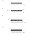
- Fig. 1 schematically a coated according to the invention substrate is shown.
- the substrate 1 is coated with a hard material layer 1.
- the hard material layer 1 comprises crystalline AlN, wherein the AlN crystallites have a (001) preferred direction. Due to the layer properties of the hard material layer 1, in particular the high hardness and a large modulus of elasticity already a layer thickness of the hard material layer 1 of only 200 nm, preferably even only 100 nm is sufficient to protect the substrate 2 from mechanical stress and scratches. Thicker layers up to 2000nm are also conceivable.
- Fig. 2 schematically shows a further embodiment in which between the substrate 2 and the hard material layer 1, a further layer 3 is arranged.
- the additional layer 3 may be, for example, a decorative layer or a bonding agent layer. Such layers 3, which consist of several partial layers, for example a decorative and a bonding agent layer, are possible.
- the substrate can be completely or even partially provided with the layer 3.
- the hard material layer is arranged above the additional layer 3, ie the additional layer 3 is thus arranged between substrate 2 and hard material layer 1.
- the layer 3 is preferably a doped AlN layer or a mixed layer. Depending on the composition of the adhesion promoter layer, for example, it may have a thermal expansion coefficient which lies between the thermal expansion coefficients of substrate 2 and hard material layer 1. Thus stresses between substrate 2 and hard material layer 1 can be reduced by the adhesion promoter layer 3.
- the adhesion promoter layer 3 preferably has a thickness in the range from 1 to 900 nm, particularly preferably in the range from 1 to 500 nm, particularly preferably in the range from 1 to 50 nm.
- the coated substrate between the glass substrate 2 and the hard material layer 1 as the adhesion promoter layer 3 has an Al 2 O 3 coating with a layer thickness of 50 nm.
- Fig. 3 is a further embodiment of the invention shown schematically.
- the cover layer 4 contains SiO 2 in this embodiment and has a layer thickness of 1 to 100 nm.
- Fig. 4 shows a further embodiment in which the coated substrate in addition to the hard material layer 1 both an additional layer 3 and a cover layer 4 has.
- Fig. 5 shows the spectrum of an EDX analysis (energy dispersive X-ray spectroscopy or energy-dispersive X-ray analysis) of an embodiment of a hard material layer according to the invention.
- the hard material layer is a silicon-doped or doped AlN layer.
- Fig. 6a a transmission electron microscopic (TEM) image of a hard material layer according to the invention is shown.
- the TEM image shown is a photograph of an AlN layer doped with SiN, ie, an AlN: SiN layer wherein the content of AlN is 75 wt% and the content of SiN is 25 wt%.
- the AlN of the hard material layer is present in crystalline form in a SiN matrix.
- an AlN: SiN layer in which AlN and SiN are in equal parts is amorphous.
- a TEM image of a corresponding layer is taken in Fig. 6b shown.
- the high content of SiN prevents the formation of AlN crystallites.
- Fig. 7 shows the XRD spectrum (X-ray diffraction, X-ray diffraction) of an embodiment of a coated substrate according to the invention.
- an SiO 2 substrate was coated with an AlN / SiN hard material layer and an XRD spectrum of the coated substrate was recorded.
- the spectrum 5 shows three reflections which can be assigned to the three orientations (100), (001) and (101) of the hexagonal crystal structure of the AlN. It becomes clear that the hard material layer predominantly has a (001) preferred direction.
- the corresponding reflex at 36 ° is much more pronounced than the reflections of the (100) orientation (33.5 °) and the (101) orientation (38 °).
- the fraction x (001) in this embodiment is 0.67 and the fraction y (001) is 0.77.
- Measurement curve 6 is the XRD spectrum of the uncoated substrate.
- the hard material layer was deposited with a sputtering power in the range> 15 W / cm 2 at a low target - substrate distance in the range of 10 to 12 cm.
- the process temperature was 250 ° C.
- Fig. 8 shows XRD spectrum of hard coatings, which, although a composition comparable to that in Fig. 7 shown embodiment, but have other preferred directions of the crystal structure.
- the spectrum 7 is to be assigned to a comparative example with a (100) preferred direction and the spectrum 8 to a comparative example with a (101) preferred direction.
- the hard material layer with the (100) preferred direction (curve 8) was deposited as with a high target substrate distance (> 15 cm) and a low sputtering power of 13 W / cm 2 .
- the process temperature was about 100 ° C.
- the hard material layer with the (101) preferred direction (curve 7) was deposited with an even lower sputtering power of 9.5 W / cm 2 .
- Target-substrate distance and process temperature correspond to the deposition conditions of the hard material layer with (100) preferred direction.
- Fig. 9a to 10b the influence of the preferred direction of the crystal structure on the mechanical resistance of the respective hard material layers can be recognized.
- Fig. 9a to 9c These are photographic exceptions of different coated substrates after a stress test with sand. In each case, sand was added to the coated substrates and this was oscillated 100 times in a container using body of appeal.
- Fig. 9a shows the image after the stress test of a sample with a coating with (101) preferred direction
- Fig. 9b a corresponding recording of a sample with (100) preferred direction
- Fig. 9c the inclusion of a sample with a (001) preferred direction according to the invention.
- Fig. 9a shows the image after the stress test of a sample with a coating with (101) preferred direction
- Fig. 9b a corresponding recording of a sample with (100) preferred direction
- Fig. 9c the inclusion of a sample with a (001) preferred direction according to the invention.
- Fig. 9a shows the image after
- the 10a and 10b show coated substrates after a mechanical load test with SiC. This stress test simulates in particular the resistance to very hard materials and the cleanability against all cleaners and auxiliaries. The test procedure is comparable to the sand test.
- the coating of in Fig. 10a shown sample has no orientation of the crystallites in (001) direction, while the coating of the in Fig. 10b shown sample has a predominant (001) orientation.
- the sample with predominant (001) orientation has substantially fewer scratches than the sample without predominant (001) orientation of the crystallites.
Landscapes
- Chemical & Material Sciences (AREA)
- Chemical Kinetics & Catalysis (AREA)
- Organic Chemistry (AREA)
- Materials Engineering (AREA)
- Engineering & Computer Science (AREA)
- Life Sciences & Earth Sciences (AREA)
- General Chemical & Material Sciences (AREA)
- Geochemistry & Mineralogy (AREA)
- Mechanical Engineering (AREA)
- Metallurgy (AREA)
- Composite Materials (AREA)
- Dispersion Chemistry (AREA)
- Physical Vapour Deposition (AREA)
- Surface Treatment Of Glass (AREA)
- Laminated Bodies (AREA)
Abstract
Description
- Die Erfindung betrifft im Allgemeinen kratzresistente Beschichtungen, Substrate mit kratzfesten Beschichtungen sowie Verfahren zu deren Herstellung. Im Speziellen betrifft die Erfindung kratzresistente Beschichtungen und entsprechend beschichtete Substrate mit einer Hartstoffschicht basierend auf Aluminiumnitrid sowie deren Herstellung, insbesondere durch Sputtern.
- Aus dem Stand der Technik sind verschiedene Beschichtungen zur Erhöhung der Kratzfestigkeit bekannt. So beschreibt die Patentanmeldung
DE 102 011 081 234 A1 eine Hartstoffbeschichtung auf Glaskeramiksubstraten, welche zwei unterschiedliche Materialphasen aufweist. Nachteilig ist jedoch, dass der thermische Ausdehnungskoeffizient der Beschichtung und des Substrates um maximal 20% voneinander abweichen dürfen. Da zudem Glaskeramiken einen sehr niedrigen thermischen Ausdehnungskoeffizienten aufweisen, grenzt dies die Anzahl der geeigneten Beschichtungen stark ein. So weisen beispielsweise Hartstoffschichten basierend auf Nitriden oder Oxiden wie Aluminiumnitrid oder Bornitrid zu große thermische Ausdehnungskoeffizienten auf, so dass diese nicht zur Beschichtung von Glaskeramiksubstraten eingesetzt werden können. - Eine Beschichtung zur Erhöhung der Kratzfestigkeit sollte nicht nur eine hohe Härte aufweisen, vielmehr sind auch Elastizität (E-Modul), Oberflächenrauhigkeit, Schichtspannungen durch unterschiedliche thermische Ausdehnungskoeffizienten von Substrat und Beschichtung sowie die Oberflächenbeschaffenheit des Substrates entscheidende Faktoren für die Güte eine kratzfesten Beschichtung bzw. des entsprechend beschichteten Substrates.
- Darüber hinaus ist es wünschenswert, dass entsprechend beschichtete Oberflächen wie beispielsweise Glas- oder Glaskeramikoberflächen neben einer hohen Kratzfestigkeit auch eine hohe Resistenz gegenüber Verschleiß- und Politurbelastungen, wie sie sowohl während der Produktion als auch der späteren Verwendung auftreten, aufweisen.
- Es ist Aufgabe der Erfindung, eine Beschichtung sowie ein entsprechend beschichtetes Substrat bereit zu stellen, welches neben einer hohen Kratzfestigkeit auch eine erhöhte Beständigkeit gegenüber Verschleiß- und Polierbelastungen sowie gegenüber Umweltbelastungen aufweist. Eine weitere Aufgabe der Erfindung besteht in der Bereitstellung eines entsprechenden Herstellungsverfahrens.
- Die Aufgabe der Erfindung wird in überraschender Art und Weise bereits durch den Gegenstand der unabhängigen Ansprüche gelöst. Vorteilhafte Ausgestaltungen und Weiterbildungen der Erfindung sind Gegenstand der Unteransprüche.
- Die erfindungsgemäße Beschichtung umfasst eine transparente, hochbrechende Hartstoffschicht auf Basis von Aluminiumnitrid (AlN), d.h. die Hartstoffschicht enthält AlN als einen wesentlichen Bestandteil. Erfindungsgemäß ist der Anteil an AlN in der Hartstoffschicht größer als 50 Gew.-%.
- Die Hartstoffschicht wirkt auch als Verschleißschutzschicht. Die Erfinder haben dabei überraschender Weise festgestellt, dass eine besonders kratzfeste und gegen Verschleiß- und Polierbelastungen resistente Beschichtung erhalten werden kann, wenn das AlN der Hartstoffschicht kristallin oder zumindest weitgehend kristallin ist und eine hexagonale Kristallstruktur aufweist. Insbesondere weist die AlN-Schicht einen Kristallisationsgrad von zumindest 50% auf.
- Dies ist insofern überraschend, da üblicherweise davon ausgegangen wird, dass amorphe Beschichtungen durch das Fehlen von Kristalliten eine geringere Oberflächenrauhigkeit aufweisen als entsprechende kristalline Beschichtungen. Eine geringe Schichtrauheit wird dabei mit einer geringeren Anfälligkeit für das Auftreten von Defekten, beispielsweise verursacht durch die Reibung eines Fremdkörpers auf der Oberfläche der Beschichtung, in Verbindung gebracht. Dennoch weist die erfindungsgemäße Beschichtung nicht nur eine hohe Kratzresistenz, sondern auch eine erhöhte Resistenz gegenüber Umwelteinflüssen sowie Polier- und Verschleißbelastungen auf. So weist die Hartstoffschicht eine hohe chemische Resistenz, beispielsweise gegenüber Reinigungsmitteln und Spülmitteln, auf. Zudem ist die erfindungsgemäße Beschichtung trotz ihrer kristallinen Struktur für Licht mit Wellenlängen im sichtbaren und infraroten Spektralbereich transparent, so dass die Beschichtung optisch unauffällig ist und beispielsweise in optischen Bauteilen wie auch als Beschichtung von Kochfeldern eingesetzt werden kann. So weist die Beschichtung insbesondere eine Transparenz für sichtbares Licht von zumindest 50%, bevorzugt von zumindest 80% bezogen auf die Normlichtart C und für infrarotes Licht eine Transparenz von zumindest 50%, bevorzugt von zumindest 80% auf.
- Bei der Hartstoffschicht handelt es sich um eine hochbrechende Schicht. So weist die Hartstoffschicht in einer Ausführungsform einen Brechwert im Bereich von 1,8 bis 2,3, bevorzugt im Bereich von 1,95 bis 2,1 bei einer Wellenlänge von 550 nm auf.
- Die hohe Transparenz der Beschichtung kann insbesondere durch die geringe Größe der einzelnen Kristallite erzielt werden. So werden durch die geringe Größe beispielsweise Streueffekte vermieden. In einer Ausführungsform der Erfindung beträgt die mittlere Kristallgröße höchstens 20 nm, bevorzugt höchstens 15 nm und besonders bevorzugt 5 bis 15 nm. Ein weiterer Vorteil der geringen Kristallgröße besteht in der höheren mechanischen Beständigkeit der die Kristallite enthaltenden Schicht. So weisen größere Kristallite häufig einen Versatz in ihrer Kristallstruktur auf, was sich nachteilig auf die mechanische Beständigkeit auswirkt.
- Die AlN-Kristallite in der Hartstoffschicht weisen eine hexagonale Kristallstruktur mit einer vorwiegenden Vorzugsrichtung in (001)-Richtung, d.h. parallel zur Substratoberfläche auf. Bei einer Kristallstruktur mit Vorzugsrichtung wird eine der Symmetrierichtungen der Kristallstruktur von den Kristalliten bevorzugt eingenommen. Im Sinne der Erfindung wird unter einer AlN-Kristallstruktur mit einer Vorzugsrichtung in (001)-Richtung insbesondere eine Kristallstruktur verstanden, die bei einer röntgendiffraktometrischen Messung im entsprechenden XRD-Spektrum im Bereich zwischen 34° und 37° eine maximale Reflexion zeigt. Die Reflexion in diesem Bereich kann dabei einer AlN-Kristallstruktur mit einer (001)-Vorzugsrichtung zugeordnet werden.
- Es konnte überraschenderweise festgestellt werden, dass erfindungsgemäße Hartstoffschichten mit einer Vorzugsrichtung in (001)-Richtung sowohl ein höheres E-Modul als auch eine größere Härte aufweisen als Hartstoffschichten mit einer gleichen oder vergleichbaren Zusammensetzung ohne (001)-Vorzugsrichtung.
- Das hohe E-Modul der Beschichtung mit einer überwiegenden(001)-Vorzugsrichtung kann damit erklärt werden, dass das Elastizitätsmodul eines kristallinen Stoffes von dessen Vorzugsrichtung abhängt. Somit ist das E-Modul in der erfindungsgemäßen Hartstoffschicht parallel zur Substratoberfläche am größten. In einer Ausführungsform der Erfindung weisen die Hartstoffschichten ein E-Modul bei einer Prüfkraft von 10 mN parallel zur Substratoberfläche im Bereich von 90 bis 250 GPa, bevorzugt im Bereich von 110 bis 200 GPa auf.
- Die Kratzfestigkeit einer Beschichtung hängt neben der Härte auch davon ab, wie gut die Beschichtung auf dem Substrat haftet. Zeigen Beschichtung und Substrat zudem unterschiedliche thermische Ausdehnungskoeffizienten, so kann dies zum Aufbau von Spannungen in der Beschichtung und zu einem Abplatzen der Beschichtung führen. Bei Beschichtungen mit einem vergleichsweise hohen E-Modul können dabei die auftretenden Spannungen besser abgefangen werden, so dass die Beschichtung besser auf dem Substrat haftet.
- Die Resistenz der Beschichtung gegenüber Abrieb ist weiterhin auch vom Verhältnis aus Härte und E-Modul der jeweiligen Schicht abhängig. Bevorzugt weisen die Schichten daher ein Verhältnis von Härte zu E-Modul von zumindest 0,08, bevorzugt 0,1, besonders bevorzugt größer als 0,1 auf. Dies kann durch die (001)-Vorzugsrichtung erreicht werden. Hinsichtlich ihrer Zusammensetzung vergleichbare Schichten mit abweichender Vorzugsrichtung zeigen hierbei vergleichsweise geringe Werte im Bereich von 0,06 bis 0,08.
- Die oben beschriebenen Eigenschaften können insbesondere erreicht werden, wenn die (001)-Vorzugsrichtung der Kristallstruktur, verglichen mit den (100)- und (101)-Richtungen, am stärksten ausgeprägt ist. Darüber hinaus ist in einer Weiterbildung der Erfindung zudem der Anteil an (100)-orientierten Kristallstrukturen größer als der Anteil an (101) orientierten Kristallstrukturen.
- Zur Bestimmung des Anteils der Kristallstruktur, die eine (001)-Vorzugsrichtung aufweist, kann wie folgt vorgegangen werden:
- Aufnahme eines XRD-Spektrums der entsprechenden Schicht unter streifenden Einfall, d.h. Dünnschichtröntgenbeugung (GIXRD)
- Bestimmung der maximalen Intensität des entsprechenden (001)-Reflexes I(001) im Bereich zwischen 34° und 37°
- Bestimmung der maximalen Intensität des (100)-Reflexes I(100) im Bereich zwischen 32° und 34°
- Bestimmung der maximalen Intensität des (101)-Reflexes I(101) im Bereich zwischen 37° und 39°
- Der Anteil der Kristallstruktur mit (001)-Vorzugsrichtung x(001) und y(001) errechnet sich wie folgt:


- Als besonders vorteilhaft hat sich ein Anteil x(001) und/oder y(001) größer 0,5, bevorzugt größer 0,6 und besonders bevorzugt größer 0,75 herausgestellt.
- Ein weiterer Vorteil der AlN-Schicht besteht in ihrer vergleichsweise hohen Wärmeleitfähigkeit. Dies ist insbesondere vorteilhaft, wenn die erfindungsgemäße Beschichtung als Kratzschutz auf Kochflächen aufgebracht wird.
- In einer Ausführungsform der Erfindung beträgt der Anteil an Sauerstoff in der AlN-Schicht maximal 10 at%, bevorzugt maximal 5 at% und besonders bevorzugt maximal 2 at%.
- Durch den niedrigen Sauerstoffgehalt in der Beschichtung wird die Bildung von Oxynitriden verhindert, welche sich nachteilig auf das Kristallwachstum, insbesondere auf die Ausbildung einer Vorzugsrichtung der Kristallstruktur, auswirken.
- Die oben beschriebenen Eigenschaften der Hartstoffschicht können insbesondere dann erzielt werden, wenn die Beschichtung durch ein Sputterverfahren aufgebracht wurde.
- Die Härte und die Performance der Kratzschutzwirkung einer erfindungsgemäßen Schicht kann auch durch eine Behandlung im Anschluss an deren Herstellung verbessert werden. Neben einer einfachen thermischen Behandlung in einem Ofen können weiterhin Blitzlampen-Heizen oder eine Behandlung mittels Laser angewendet werden. Auch eine Implantation durch Ionen oder Elektronen ist denkbar. Hierdurch kann eine (001)-Vorzugsrichtung der Kristallstruktur erhalten oder deren Anteil x(001) und/oder y(001) in der Kristallstruktur weiter erhöht werden.
- Für den Einsatz der Beschichtungen im Bereich Kochfeld ist es wichtig, dass sich die Töpfe leicht über das Kochfeld schieben lassen. Solche Töpfe bestehen insbesondere aus Edelstahl. Bevorzugt weist daher die Beschichtung eine Haftreibung µ gegenüber Metallkörpern < 0,5, besonders bevorzugt < 0,25 auf.
- Bei der AlN-Schicht bzw. Hartstoffschicht kann es sich um eine reine Aluminiumnitridschicht handeln oder die Hartstoffschicht kann neben Aluminiumnitrid weitere Bestandteile, beispielsweise ein oder mehrere weitere Nitride, Carbide und/oder Carbonitride enthalten. Bevorzugt handelt es sich bei den Nitriden, Carbiden oder Carbonitriden um die entsprechenden Verbindungen der Elemente Silizium, Bor, Zirkon, Titan, Nickel, Chrom oder Kohlenstoff. Hierdurch können Eigenschaften der Hartstoffschicht wie beispielsweise Härte, E-Modul oder die Widerstandsfähigkeit gegen Abrieb, beispielsweise die Polierresistenz, weiter modifiziert werden.
- Um zu gewährleisten, dass sich auch bei diesen Ausführungsformen eine kristalline Aluminiumnitridphase ausbildet, ist ein Aluminiumgehalt der Hartstoffschicht > 50 Gew.-%, bevorzugt > 60 Gew.-% und besonders bevorzugt > 70 Gew.-%, jeweils bezogen auf die zusätzlichen Elemente Silizium, Bor, Zirkon, Titan, Nickel, Chrom und/oder Kohlenstoff, besonders vorteilhaft.
- Entsprechende Mischschichten werden im Sinne der Erfindung auch als dotierte AlN-Schichten bezeichnet. Die zusätzlich zum AlN enthaltenen Verbindungen werden im Sinne der Erfindung als Dopant bezeichnet, wobei der Gehalt an Dopant bis zu 50 Gew.-% betragen kann. Hierbei werden unter dotierten Schichten im Sinne der Erfindung auch Schichten, die einen Gehalt von bis zu 50 Gew.-% an Dopant enthalten, verstanden.
- Bei Mischschichten bzw. dotierten AlN-Schichten sind AlN-Kristallite in einer Matrix des Dopants eingebettet. Der Kristallisationsgrad der Schicht kann somit über den Anteil des Dopants in der Mischschicht eingestellt werden. Zudem wird die Kristallitgröße durch die Matrix begrenzt. Als besonders vorteilhaft hat sich dabei eine Kristallitgröße von maximal 20 nm, bevorzugt von maximal 15 nm herausgestellt. Insbesondere liegt die mittlere Größe der AlN-Kristallite im Bereich von 5 bis 15 nm. Diese Kristallitgröße gewährleistet eine hohe Transparenz und mechanische Beständigkeit der Hartstoffschicht.
- In einer Ausführungsform der Erfindung enthält die Hartstoffschicht neben Aluminiumnitrid Bornitrid, d.h. die Schicht ist mit Bornitrid dotiert. Durch das enthaltene Bornitrid wird der Reibwert der Schicht reduziert, was insbesondere zu einer höheren Resistenz der Schicht gegenüber Polierprozessen führt. Dies ist sowohl in Hinblick auf die Beständigkeit eines entsprechend beschichteten Substrates bei der Verwendung durch den Endverbraucher wie auch in Hinblick auf mögliche Verfahrensschritte bei der Weiterverarbeitung des beschichteten Substrates vorteilhaft.
- In einer anderen Ausführungsform der Erfindung ist die Hartstoffschicht mit Siliziumnitrid dotiert, d.h. es handelt sich um ein AlN:SiN-Materialsystem, durch welches einzelne Eigenschaften wie z.B. die Haftung, die Härte, die Rauigkeit, der Reibwert und/oder die thermische Beständigkeit beeinflusst werden können. In einer Weiterbildung dieser Ausführungsform weist die Hartstoffschicht zumindest einen weiteren Dopanten auf.
- Des Weiteren kann der thermische Ausdehnungskoeffizient der Hartstoffschicht durch Art und Menge des eingesetzten Dopants beeinflusst werden oder auf das Substrat adaptiert werden.
- Eine Weiterbildung der Erfindung sieht vor, dass die Beschichtung zusätzlich zur Hartstoffschicht zumindest eine weitere Schicht aufweist. Gemäß einer Ausführungsform weist die Beschichtung neben der Hartstoffschicht eine Deckschicht auf, welche oberhalb der Hartstoffschicht angeordnet ist. Die Bezeichnung oberhalb bezieht sich auf den Aufbau der Beschichtung ausgehend vom Substrat, d.h. die Hartstoffschicht ist somit zwischen dem Substrat und der Deckschicht angeordnet. Durch das Aufbringen einer Deckschicht auf die Hartstoffschicht können einzelne Eigenschaften wie z.B. das optische Erscheinungsbild oder die Poliereigenschaften gegenüber einem bestimmten Poliermedium modifiziert werden.
- Eine Ausführungsform der Erfindung sieht vor, dass die Deckschicht durch Nitride, Oxide, Carbide, Carbonitride und/oder Oxinitride ausgewählt aus der Gruppe der Elemente Aluminium, Silizium, Bor, Zirkon, Titan, Nickel oder Kohlenstoff gebildet wird. Die Deckschicht kann als eine Mischschicht mehrerer der oben genannten Verbindungen oder als eine Schicht einer Verbindung ausgebildet sein. Bevorzugt wird die Deckschicht durch Sputtern aufgebracht. Alternativ können auch CVD oder Sol Gel Technologien eingesetzt werden.
- Bei der Deckschicht kann es sich beispielsweise um eine SiO2-haltige Schicht handeln. Abhängig von der Schichtdicke der Deckschicht kann somit beispielsweise der Farbort der Reflexionsfarbe und/oder die Reflexionseigenschaften der Beschichtung verändert werden.
- In einer weiteren Ausführungsform weist die Hartstoffschicht eine kohlenstoffhaltige Deckschicht auf. Der Kohlenstoffgehalt der Deckschicht führt dabei zu einer Verringerung des Reibwertes, was insbesondere bei beschichteten Substraten, die als Kochfläche verwendet werden, vorteilhaft ist, da sich so die Topfe leichter auf dem Kochfeld verschieben lassen. Des Weiteren können die Poliereigenschaften und die Resistenz der Beschichtung gegenüber Poliermedien verbessert werden. Die Deckschicht kann beispielsweise Carbide und/oder Graphit enthalten.
- Alternativ oder zusätzlich kann die Beschichtung eine Haftvermittlerschicht aufweisen. Diese ist zwischen dem Substrat und der Hartstoffschicht angeordnet und verbessert die Anhaftung der Hartstoffschicht auf dem Substrat. Dies ist insbesondere dann vorteilhaft, wenn die thermischen Ausdehnungskoeffizienten von Substrat und Hartstoffschicht sich deutlich unterscheiden. Als besonders vorteilhaft haben sich hierbei solche Haftvermittlerschichten herausgestellt, die aus Nitriden, Oxiden, Carbiden, Carbonitriden und/oder Oxynitriden der Elemente Aluminium, Silizium, Bor, Zirkon, Titan, Nickel, Chrom und/oder Kohlenstoff gebildet werden.
- Die Haftvermittlerschicht kann hierbei auftretende Spannungen reduzieren, zumindest führt sie zu einer starken chemischen Anbindung an das Substrat. Eine entsprechende enge Anpassung der thermischen Ausdehnungskoeffizienten von Substrat und Hartstoffschicht ist daher nicht notwendig. Dies ermöglicht eine breite Auswahl an geeigneten Substratmaterialien. Die Abscheidung kann beispielsweise über PVD, CVD oder Sol-Gel-Verfahren erfolgen.
- Als Substrate können somit insbesondere Gläser, bevorzugt Saphirgläser, Borosilikatgläser, Aluminosilikatgläser, Kalk-Natrongläser, synthetische Quarzgläser (sog. fused silica Gläser), Lithiumaluminosilikatgläser oder optische Gläser verwendet werden. Auch Kristalle für optische Anwendungen wie z.B. Kaliumfluoridkristalle oder Glaskeramiken können als Substrat verwendet werden.
- In einer bevorzugten Ausführungsform handelt es sich bei dem Substrat um eine Glaskeramik, insbesondere um eine Glaskeramik mit einem thermischen Ausdehnungskoeffizienten α20-300 kleiner als 2*10-6 K-1. Entsprechende Glaskeramiken können beispielsweise als Kochflächen verwendet werden. Da die erfindungsgemäßen Beschichtungen zudem gegenüber Temperaturen von zumindest 300°C, bevorzugt von zumindest 400°C dauerhaft stabil sind, kann die Beschichtung auch auf den Heißzonen des Kochfeldes aufgebracht werden.
- Auf Grund der hohen Temperaturstabilität kann die Beschichtung bzw. entsprechend beschichtete Glassubstrate in anderen Heißbereichen, beispielsweise als Ofensichtscheibe, verwendet werden.
- Insbesondere bei Kochfeldern wird häufig ein Dekor auf die Glaskeramikoberfläche aufgedruckt. Eine Ausführungsform sieht daher vor, dass das Substrat zumindest teilweise mit einer Dekorschicht versehen wird und die Dekorschicht zwischen dem Substrat und der Beschichtung angeordnet ist. Auf Grund der hohen Transparenz der erfindungsgemäßen Beschichtung ist das Dekor durch die Beschichtung gut wahrnehmbar. Zudem wird die Dekorschicht durch die Hartstoffschicht vor mechanischen Belastungen geschützt, so dass an die Dekorschicht geringere Anforderungen in Hinblick auf deren mechanische Belastbarkeit gestellt werden können.
- Das mit der erfindungsgemäßen Hartstoffschicht beschichtete Substrat kann insbesondere als optisches Bauteil, Kochfläche, Sichtscheiben im Fahrzeugbereich, Uhrengläsern, Glas- oder Glaskeramikbauteile in Haushaltsgeräten, Ofensichtscheiben oder als Display beispielsweise für Tablet-PCs oder Mobiltelefone, insbesondere als Touchdisplay verwendet werden.
- Die Hartstoffschichten bzw. das erfindungsgemäß beschichtete Substrat kann dabei insbesondere mit einem Verfahren hergestellt werden, dass zumindest die folgenden Schritte umfasst:
- a) Bereitstellen eines Substrates in einer Sputtervorrichtung mit einem aluminiumhaltigen Target
- b) Abgabe von gesputterten Partikeln mit einer Leistung im Bereich von 8 bis 1000 W/cm2, bevorzugt 10 - 100 W/cm2 pro Targetfläche.
- Die Beschichtung des Substrates in Schritt b) erfolgt dabei ab niedrigen Enddrücken. So liegt der Enddruck in der Beschichtungsanlage, d.h. der Druck, ab dem ein Beschichtungsvorgang gestartet werden kann, bei höchstens 2*10-5 mbar, bevorzugt sogar bei Drücken im Bereich von 1*10-6 bis 5*10-6 mbar. Durch die geringen Enddrücke wird die Fremdgasmenge minimiert, d.h. der Beschichtungsprozess wird in einer sehr reinen Atmosphäre durchgeführt. Dies gewährleistet eine hohe Reinheit der aufgebrachten Schichten. So wird durch prozessbedingten geringen Restgasgehalt die Bildung von Oxynitriden durch den Einbau von Sauerstoff vermieden. Dies ist insbesondere in Hinblick auf das Kristallwachstum der AlN-Kristallite von Bedeutung, da dieses durch Oxynitride gestört wird. Bevorzugt kann somit eine Beschichtung mit einem Sauerstoffgehalt von maximal 10 at-%, besonders bevorzugt von maximal 5 at-% oder sogar maximal 2 at-% erhalten werden. Dagegen wird bei konventionellen Sputterverfahren mit einem Endruck im Bereich von zumindest 5*10-5 mbar beschichtet, entsprechend ist hier der Sauerstoffanteil in der abgeschiedenen Beschichtung höher.
- Beim Sputterprozess wird nach Erreichen des erfindungsgemäßen Enddrucks ein stickstoffhaltiges Prozessgas eingeleitet. Der Anteil des Stickstoffs am Gesamtfluss beträgt zumindest 30 Vol.-%, bevorzugt zumindest 40 Vol.-% und besonders bevorzugt zumindest 50 Vol.-% . Über den Anteil des Stickstoffs am Gesamtfluss während des Sputterprozesses kann die chemische Resistenz der abgeschiedenen Schicht, beispielsweise gegenüber Spülmitteln oder Reinigungsmitteln beeinflusst werden. So steigt die Resistenz der Schicht gegenüber Chemikalien mit steigendem Stickstoffanteil.
- Die Beschichtung in Schritt b) erfolgt mit hohen Sputterleistungen. Die Sputterleistungen im erfindungsgemäßen Verfahren betragen hierbei zumindest 8 - 1000 W/cm2, bevorzugt zumindest 10 - 100 W/cm2. In einer Ausführungsform der Erfindung wird ein Magnetronsputtern oder ein High Power Impulse Magnetron Sputtering-Verfahren (HiPIMS) angewendet. Alternativ oder zusätzlich kann zwischen dem Target und dem Substrat eine negative Spannung oder eine Wechselspannung aufrechterhalten werden. Die Beschichtung kann alternativ oder zusätzlich mit Unterstützung von Ionenbeschuss, bevorzugt mit Ionenbeschuss aus einer Ionenstrahlquelle und/oder durch Anlegen einer Spannung am Substrat erfolgen.
- Gemäß einer Ausführungsform der Erfindung werden die durch das Sputtern erzeugten Partikel bei einer Depositionstemperatur größer als 100°C, bevorzugt größer 200°C und besonders bevorzugt größer 300°C abgeschieden. In Kombination mit den niedrigen Prozessdrücken sowie der hohen Sputterleistungen kann somit das Wachstum der AlN-Kristallite, insbesondere die Kristallitgröße und die Vorzugsrichtung der Kristallstruktur, in besonders vorteilhafter Weise beeinflusst werden. Es ist jedoch auch eine Abscheidung bei niedrigeren Temperaturen, beispielsweise bei Raumtemperatur, möglich. Die gemäß dieser Ausführungsform hergestellten Hartstoffschichten zeigen ebenfalls gute mechanische Eigenschaften wie eine hohe Kratzresistenz.
- Bei dem Sputterprozess kann es sich um eine kontinuierliche Deposition auf dem Substrat handeln. Alternativ kann der Sputtervorgang auch derart durchgeführt werden, dass die abgeschiedenen Schichten Interfaces aufweisen bzw. aus Interfaces bestehen, welche auf Grund der Prozessierung beim Herausfahren aus dem Beschichtungsbereich entstehen.
- In Schritt a) kann als Substrat beispielsweise eine Glaskeramik, ein Saphirglas, ein Borosilikatglas, ein Aluminosilikatglas, ein Kalk-Natronglas, ein synthetisches Quarzglas, ein Lithiumaluminosilikatglas, ein optisches Glas und/oder ein Kristall für optische Zwecke bereit gestellt werden.
- In einer Ausführungsform der Erfindung enthält das Target neben Aluminium zumindest eines der Elemente Silizium, Bor, Zirkon, Titan oder Kohlenstoff. Diese zusätzlichen Elemente neben Aluminium werden im Sinne der Erfindung auch als Dopant bezeichnet. Bevorzugt ist der Anteil an Aluminium im Target größer als 50 Gew.-%, besonders bevorzugt größer 60 Gew.-% und ganz besonders bevorzugt größer als 70 Gew.-%.
- In einer Weiterbildung der Erfindung wird in Schritt a) ein Substrat bereitgestellt, welches eine Dekor und/oder eine Haftvermittlerschicht aufweist.
- So ist beispielsweise eine Beschichtung von zumindest teilweise dekorierten Bereichen möglich und bleibt auch bei hohen Anwendungstemperaturen resistent. Auch Flachfacetten sind ohne optische Veränderungen beschichtbar und zeigen eine gute mechanische Beständigkeit.
- Alternativ oder zusätzlich wird in einem dem Schritt b) nachfolgenden Verfahrensschritt eine Deckschicht auf der Hartstoffschicht aufgebracht.
- Gemäß einer Ausführungsform der Erfindung enthält die Haftvermittlerschicht und/oder die Deckschicht Nitride, Oxide, Carbide, Carbonitride und/oder Oxynitride eines oder mehrerer Elemente ausgewählt aus der Gruppe umfassend Aluminium, Silizium, Bor, Zirkon, Titan, Nickel und Kohlenstoff.
- Bevorzugt werden Haftvermittlerschicht und/oder Deckschicht durch einen Sputterprozess aufgebracht.
- Nachfolgend wird die Erfindung an Hand von Figuren und Ausführungsbeispielen näher erläutert. Es zeigen dabei:
-
Fig. 1 eine schematische Darstellung eines erfindungsgemäß beschichteten Substrates, -
Fig. 2 eine schematische Darstellung einer Ausführungsform der Erfindung mit zusätzlicher Haftvermittlerschicht, -
Fig. 3 eine schematische Darstellung einer Ausführungsform der Erfindung mit zusätzlicher Deckschicht, -
Fig. 4 eine schematische Darstellung einer Ausführungsform der Erfindung mit zusätzlicher Haftvermittlerschicht und zusätzlicher Deckschicht, -
Fig. 5 ein EDX-Spektrum einer dotierten AlN-Hartstoffschicht, -
Fig. 6a und 6b TEM-Aufnahmen zweier mit AlN-SiN-Mischschichten mit unterschiedlichem AlN-Gehalten, -
Fig. 7 das XRD-Spektrum eines Ausführungsbeispiels, -
Fig. 8 die XRD-Spektren zweier AlN-Hartstoffschichten mit unterschiedlichen Vorzugsrichtungen, -
Fig. 9a bis 9c fotografische Aufnahmen verschiedener beschichteter Substrate mit unterschiedlichen Vorzugsrichtungen nach einem mechanischen Belastungstest mit Sand und -
Fig. 10a und 10b fotografische Aufnahmen verschiedener beschichteter Substrate mit unterschiedlichen Vorzugsrichtungen der Kristallstruktur nach einem mechanischen Belastungstest mit Siliziumcarbid. - In
Fig. 1 wird schematisch ein erfindungsgemäß beschichtetes Substrat dargestellt. Hierbei ist das Substrat 1 mit einer Hartstoffschicht 1 beschichtet. Die Hartstoffschicht 1 umfasst kristallines AlN, wobei die AlN-Kristallite eine (001)-Vorzugsrichtung aufweisen. Auf Grund der Schichteigenschaften der Hartstoffschicht 1, insbesondere der großen Härte sowie eines großen E-Moduls ist bereits eine Schichtdicke der Hartstoffschicht 1 von nur 200 nm, bevorzugt sogar von nur 100 nm ausreichend, um das Substrat 2 vor mechanischen Belastungen und Kratzern zu schützen. Dickere Schichten bis 2000nm sind aber ebenfalls denkbar. -
Fig. 2 zeigt schematisch ein weiteres Ausführungsbeispiel, bei dem zwischen dem Substrat 2 und der Hartstoffschicht 1 eine weitere Schicht 3 angeordnet ist. Bei der zusätzlichen Schicht 3 kann es sich beispielsweise um eine Dekorschicht oder eine Haftvermittlerschicht handeln. Auch solche Schichten 3, die aus mehreren Teilschichten, beispielsweise einer Dekor- und einer Haftvermittlerschicht, bestehen, sind möglich. Das Substrat kann dabei vollständig oder auch nur teilweise mit der Schicht 3 versehen werden. Die Hartstoffschicht ist dabei über der zusätzlichen Schicht 3 angeordnet, d.h. die zusätzliche Schicht 3 ist somit zwischen Substrat 2 und Hartstoffschicht 1 angeordnet. - Bei Ausführungsformen mit einer Haftvermittlerschicht als zusätzliche Schicht 3 handelt es sich bei der Schicht 3 bevorzugt um eine dotierte AlN-Schicht bzw. eine Mischschicht. Abhängig von der Zusammensetzung der Haftvermittlerschicht kann diese beispielsweise einen thermischen Ausdehnungskoeffizienten aufweisen, welcher zwischen den thermischen Ausdehnungskoeffizienten von Substrat 2 und Hartstoffschicht 1 liegt. Somit können Spannungen zwischen Substrat 2 und Hartstoffschicht 1 durch die Haftvermittlerschicht 3 verringert werden. Bevorzugt weist die Haftvermittlerschicht 3 eine Dicke im Bereich von 1 bis 900 nm, besonders bevorzugt im Bereich von 1 bis 500nm, besonders bevorzugt im Bereich von 1 bis 50nm auf. Gemäß einem Ausführungsbeispiel weist das beschichtete Substrat zwischen Glassubstrat 2 und der Hartstoffschicht 1 als Haftvermittlerschicht 3 eine Al2O3-Beschichtung mit einer Schichtdicke von 50nm auf.
- In
Fig. 3 ist eine weitere Ausführungsform der Erfindung schematisch dargestellt. Hierbei wird eine Deckschicht 4 auf die Hartstoffschicht 1 aufgebracht. Die Deckschicht 4 enthält in diesem Ausführungsbeispiel SiO2 und weist eine Schichtdicke von 1 bis 100 nm auf. -
Fig. 4 zeigt ein weiteres Ausführungsbeispiel, bei dem das beschichtete Substrat neben der Hartstoffschicht 1 sowohl eine zusätzliche Schicht 3 als auch eine Deckschicht 4 aufweist. -
Fig. 5 zeigt das Spektrum einer EDX-Analyse (energy dispersive X-ray spectroscopy bzw. energiedispersive Röntgenanalyse) eines Ausführungsbeispiels einer erfindungsgemäßen Hartstoffschicht. Es handelt sich in diesem Ausführungsbeispiel bei der Hartstoffschicht um eine mit Silizium legierte bzw. dotierte AlN-Schicht. - In
Fig. 6a ist eine transmissionselektronenmikroskopische (TEM) Aufnahme einer erfindungsgemäßen Hartstoffschicht abgebildet. Bei dem inFig. 6a gezeigten TEM-Bild handelt es sich um eine Aufnahme einer AlN-Schicht, die mit SiN dotiert wurde, d.h. eine AlN:SiN Schicht wobei der Gehalt an AlN 75 Gew.-% und der Gehalt an SiN 25 Gew.-% beträgt. An Hand derFig. 6a ist dabei ersichtlich, dass das AlN der Hartstoffschicht kristallin in einer SiN-Matrix vorliegt. Im Gegensatz dazu ist eine AlN:SiN Schicht, bei der AlN und SiN zu gleichen Teilen vorliegen, amorph. Eine TEM-Aufnahme einer entsprechenden Schicht wird inFig. 6b gezeigt. Der hohe Gehalt an SiN verhindert hierbei die Bildung von AlN-Kristalliten. -
Fig. 7 zeigt das XRD-Spektrum (X-ray diffraction, Röntgenbeugung) eines Ausführungsbeispiels eines erfindungsgemäß beschichteten Substrates. Bei diesem Ausführungsbeispiel wurde ein SiO2-Substrat mit einer AlN/SiN-Hartstoffschicht beschichtet und ein XRD-Spektrum des beschichteten Substrates aufgenommen. Das Spektrum 5 zeigt dabei drei Reflexe, die den drei Orientierungen (100), (001) und (101) der hexagonalen Kristallstruktur des AlN zugeordnet werden können. Hierbei wird deutlich, dass die Hartstoffschicht vorwiegend eine (001)-Vorzugsrichtung aufweist. Der entsprechende Reflex bei 36° ist dabei wesentlich stärker ausgeprägt als die Reflexe der (100)-Orientierung (33,5°) und der (101)-Orientierung (38°). - Der Anteil der Kristallstruktur mit (001)-Vorzugsrichtung kann dabei aus dem Spektrum 7 wie folgt bestimmt werden:
I(001) [counts] I(100) [counts] I(010) [counts] 21000 10000 6000 

- Der Anteil x(001) beträgt bei diesem Ausführungsbeispiel 0,67 und der Anteil y(001) 0,77.
- Bei der Messkurve 6 handelt es sich um das XRD-Spektrum des unbeschichteten Substrates.
- Die Hartstoffschicht wurde dabei mit einer Sputterleistung im Bereich >15 W/cm2 bei einem geringen Target - Substratabstand im Bereich von 10 bis 12 cm abgeschieden. Die Prozesstemperatur betrug 250°C.
-
Fig. 8 zeigt XRD-Spektrum von Hartstoffschichten, die zwar eine vergleichbare Zusammensetzung wie das inFig. 7 gezeigte Ausführungsbeispiel, jedoch andere Vorzugsrichtungen der Kristallstruktur aufweisen. So ist das Spektrum 7 einem Vergleichsbeispiel mit einer (100)-Vorzugsrichtung und das Spektrum 8 einem Vergleichsbeispiel mit einer (101)-Vorzugsrichtung zuzuordnen. - Die Hartstoffschicht mit der (100)-Vorzugsrichtung (Kurve 8) wurde dabei wie mit einem hohen Target-Substratabstand (> 15 cm) und einer geringen Sputterleistung von 13 W/cm2 abgeschieden. Die Prozesstemperatur lag bei ca. 100°C. Die Hartstoffschicht mit der (101)-Vorzugsrichtung (Kurve 7) wurde mit einer noch geringeren Sputterleistung von 9,5 W/cm2 abgeschieden. Target-Substrat-Abstand sowie Prozesstemperatur entsprechen dabei den Abscheidebedingungen der Hartstoffschicht mit (100)-Vorzugsrichtung.
- Anhand der
Fig. 9a bis 10b ist dabei der Einfluss der Vorzugsrichtung der Kristallstruktur auf die mechanische Beständigkeit der jeweiligen Hartstoffschichten zu erkennen. In denFig. 9a bis 9c handelt es sich um fotografische Ausnahmen verschiedener beschichteter Substrate nach einem Belastungstest mit Sand. Hierbei wurde jeweils Sand auf die beschichteten Substrate gegeben und dieser unter Verwendung von Beschwerdekörpern 100-fach in einem Behältnis oszilliert.Fig. 9a zeigt dabei die Aufnahme nach dem Belastungstest einer Probe mit einer Beschichtung mit (101)-Vorzugsrichtung,Fig. 9b eine entsprechende Aufnahme einer Probe mit (100)-Vorzugsrichtung undFig. 9c die Aufnahme einer Probe mit einer erfindungsgemäßen (001)-Vorzugsrichtung. Wie aus denFig. 9a bis 9c deutlich wird, weisen die Proben mit (101)- und (100)-Vorzugsrichtung nach dem Belastungstest eine wesentlich höhere Anzahl an Kratzern auf als die Probe mit einer (001)-Vorzugsrichtung. Bei der inFig. 9c gezeigten Probe handelt es sich dabei um das Ausführungsbeispiel, dessen XRD-Spektrum inFig. 7 abgebildet wird. - Die
Fig. 10a und 10b zeigen beschichtete Substrate nach einem mechanischen Belastungstest mit SiC. Dieser Belastungstest simuliert insbesondere die Resistenz gegenüber sehr harten Materialien und die Reinigbarkeit gegenüber jeglichen Reinigern und Hilfsmitteln. Der Testablauf ist vergleichbar zum Sandtest. Die Beschichtung der inFig. 10a gezeigten Probe weist dabei keine Ausrichtung der Kristallite in (001)-Richtung auf, während die Beschichtung der inFig. 10b gezeigten Probe eine vorwiegende (001)-Ausrichtung aufweist. Bei dem Vergleich derFig. 10a und 10b wird deutlich, dass die Probe mit vorwiegender (001)-Ausrichtung wesentlich weniger Kratzer aufweist als die Probe ohne vorwiegende (001)-Ausrichtung der Kristallite.
Claims (16)
- Substrat mit einer Beschichtung zur Erhöhung der Kratzfestigkeit, wobei die Beschichtung zumindest eine hochbrechende, transparente Hartstoffschicht umfasst, wobei die Hartstoffschicht kristallines Aluminiumnitrid enthält und wobei das Aluminiumnitrid eine hexagonale Kristallstruktur mit einer vorwiegenden (001)-Vorzugsrichtung der hexagonalen Symmetrie aufweist.
- Substrat gemäß Anspruch 1, wobei der Anteil der Kristallstruktur mit (001)-Vorzugsrichtung x(001)

und/oder
bestimmt mit Hilfe einer XRD-Messung der Beschichtung größer 0,5, bevorzugt größer 0,6 und besonders bevorzugt größer 0,75 ist. - Substrat einem der vorstehenden Ansprüche, wobei das E-Modul der Beschichtung bei einer Prüfkraft von 10 mN 80 bis 250 GPa, bevorzugt 110 bis 200 GPa und/oder Verhältnis von Härte zu E-Modul zumindest 0,08, bevorzugt zumindest 0,1, und besonders bevorzugt > 0,1 ist.
- Substrat gemäß einem der vorstehenden Ansprüche, wobei die mittlere Kristallgröße höchstens 25 nm, bevorzugt höchstens 15 nm und besonders bevorzugt 5 bis 15 nm beträgt.
- Substrat gemäß einem der vorstehenden Ansprüche, wobei das Aluminiumnitrid der Hartstoffschicht mit einem oder mehreren Nitriden, Carbiden und/oder Carbonitriden ausgewählt aus der Gruppe der Elemente Silizium, Bor, Zirkon, Titan, Nickel, Chrom oder Kohlenstoff dotiert ist und wobei der Aluminiumgehalt in der Hartstoffschicht bezogen auf das Dotiermaterial bevorzugt größer als 50 Gew.-%, besonders bevorzugt größer als 60 Gew.-% und ganz besonders bevorzugt größer als 70 Gew.-% ist.
- Substrat gemäß einem der vorherigen Ansprüche, wobei der Anteil an Sauerstoff in der Hartstoffschicht maximal 10 at%, bevorzugt weniger als 5 at% und besonders bevorzugt weniger als 2 at% beträgt.
- Substrat gemäß einem der vorherigen Ansprüche, wobei die Beschichtung eine zusätzliche Deckschicht, bevorzugt eine Deckschicht aus Nitriden, Oxiden, Carbiden, Carbonitriden und/oder Oxinitriden ausgewählt aus der Gruppe der Elemente Aluminium, Silizium, Bor, Zirkon, Titan oder Kohlenstoff,aufweist, welche oberhalb der Hartstoffschicht angeordnet ist und/oder
zwischen dem Substrat und der Hartstoffschicht eine Haftvermittlerschicht, bevorzugt eine Haftvermittlerschicht gebildet aus Nitriden, Oxiden, Carbiden, Carbonitriden und/oder Oxinitriden ausgewählt aus der Gruppe der Elemente Aluminium, Silizium, Bor, Zirkon, Titan, Nickel, Chrom oder Kohlenstoff angeordnet ist und/oder das Substrat zumindest teilweise dekorierte Bereiche aufweist, wobei die dekorierten Bereiche zwischen dem Substrat und der Beschichtung angeordnet sind. - Substrat gemäß einem der vorherigen Ansprüche, wobei das Substrat ein Glas, bevorzugt ein Saphirglas, ein Borosilikatglas, ein Aluminosilikatglas, ein Kalk-Natronglas, ein synthetisches Quarzglas, ein Lithiumaluminosilikatglas, ein optisches Glas, ein Kristall für optische Zwecke oder eine Glaskeramik, bevorzugt eine Glaskeramik mit einem thermischen Ausdehnungskoeffizienten α20-300 kleiner als 2*10-6 K-1 ist.
- Substrat gemäß einem der vorherigen Ansprüche, wobei die Beschichtung gegenüber Temperaturen von zumindest 300°C, bevorzugt von zumindest 400°C dauerhaft stabil ist und/oder die Beschichtung für Licht mit Wellenlängen im sichtbaren und/oder infraroten Bereich eine Transparenz T von zumindest 50%, bevorzugt von zumindest 80% aufweist.
- Verfahren zur Herstellung einer kratzfesten Beschichtung mit einer kristallinen aluminiumnitridhaltigen Hartstoffschicht auf einem Substrat, mit folgenden Schrittena) Bereitstellen eines Substrates in einer Sputtervorrichtung mit einem aluminiumhaltigen Targetb) Abgabe von gesputterten Partikeln mit einer Leistungsdichte im Bereich von 8 bis 1000 W/cm2 , bevorzugt 10 - 100 W/cm2 pro Targetfläche, ab Endrücken von maximal 2*10-5 mbar.
- Verfahren gemäß Anspruch 10, wobei als Sputterverfahren das Magnetronsputtern oder HiPIMS (High Power Impulse Magnetron Sputtering)- Verfahren angewendet wird,
eine negative Spannung oder eine Wechselspannung zwischen Target und Substrat aufrechterhalten wird,
die Beschichtung mit Unterstützung von Ionenbeschuss, bevorzugt mit Ionenbeschuss aus einer Ionenstrahlquelle und/oder durch Anlegen einer Spannung am Substrat erfolgt und/oder die Hartstoffschicht auf einem Substrat mit aufgerauter oder geätzter Oberfläche abgeschieden wird. - Verfahren gemäß einem der Ansprüche 10 oder 11, wobei als Target ein Aluminiumtarget mit einer Dotierung durch zumindest eines der Elemente Silizium, Bor, Zirkon, Titan, Nickel, Chrom oder Kohlenstoff verwendet wird, wobei das Target bevorzugt einen Aluminiumgehalt größer als 50 Gew.-%, besonders bevorzugt größer 60 Gew.-% und ganz besonders bevorzugt größer 70 Gew.-% aufweist.
- Verfahren gemäß einem der Ansprüche 10 bis 12, wobei das in Schritt a) bereitgestellte Substrat eine Dekorschicht und/oder eine Haftvermittlerschicht, bevorzugt eine Haftvermittlerschicht aus Nitriden, Oxiden, Carbiden, Carbonitriden und/oder Oxinitriden ausgewählt aus der Gruppe der Elemente Aluminium, Silizium, Bor, Zirkon, Titan, Nickel, Chrom oder Kohlenstoff, aufweist.
- Verfahren gemäß einem der Ansprüche 10 bis 23, wobei in einem dem Schritt b) nachfolgendem Schritt eine Deckschicht, bevorzugt eine Deckschicht aus Nitriden, Oxiden, Carbiden, Carbonitriden und/oder Oxinitriden ausgewählt aus der Gruppe der Elemente Aluminium, Silizium, Bor, Zirkon, Titan, Nickel oder Kohlenstoff, auf der Hartstoffschicht aufgebracht wird.
- Verfahren gemäß einem der vorherigen Ansprüche 10 bis 14, wobei die Partikel in Schritt b) bei Enddrücken im Bereich kleiner 2*10-5 mbar, bevorzugt im Bereich von 1*10-6 bis 5*10-6 mbar abgeschieden werden und/oder der Stickstoffanteil am Gesamtfluss zumindest 30 Vol.-%, bevorzugt zumindest 40 Vol.-% und besonders bevorzugt zumindest 50 Vol.-% beträgt.
- Verwendung eines beschichteten Substrates gemäß einem der Ansprüche 1 bis 9 als optisches Bauteil, Kochfläche, Displays oder Sichtscheiben im Fahrzeugbereich, Uhrengläsern, Ofensichtscheibe, Glas- oder Glaskeramikbauteile in Haushaltsgeräten oder als Display beispielsweise für Tablet-PCs oder Mobiltelefone, insbesondere als Touchdisplay.
Applications Claiming Priority (1)
| Application Number | Priority Date | Filing Date | Title |
|---|---|---|---|
| DE102014104799.0A DE102014104799B4 (de) | 2014-04-03 | 2014-04-03 | Substrat mit einer Beschichtung zur Erhöhung der Kratzfestigkeit, Verfahren zu dessen Herstellung und dessen Verwendung |
Publications (2)
| Publication Number | Publication Date |
|---|---|
| EP2942333A1 true EP2942333A1 (de) | 2015-11-11 |
| EP2942333B1 EP2942333B1 (de) | 2017-06-28 |
Family
ID=52780872
Family Applications (1)
| Application Number | Title | Priority Date | Filing Date |
|---|---|---|---|
| EP15160968.2A Active EP2942333B1 (de) | 2014-04-03 | 2015-03-26 | Kratzresistente beschichtungen, substrate mit kratzfesten beschichtungen und verfahren zu deren herstellung |
Country Status (6)
| Country | Link |
|---|---|
| US (1) | US9574262B2 (de) |
| EP (1) | EP2942333B1 (de) |
| JP (1) | JP6639101B2 (de) |
| KR (1) | KR102313266B1 (de) |
| CN (1) | CN104973797B (de) |
| DE (1) | DE102014104799B4 (de) |
Cited By (2)
| Publication number | Priority date | Publication date | Assignee | Title |
|---|---|---|---|---|
| DE202018104880U1 (de) | 2018-08-24 | 2018-09-13 | Schott Ag | Kochgeräte mit erhöhtem Bedienkomfort, intuitiver Steuerung und verbesserter Nutzersicherheit |
| DE102018120740A1 (de) | 2018-08-24 | 2019-02-14 | Schott Ag | Kochgeräte mit erhöhtem Bedienkomfort, intuitiver Steuerung und verbesserter Nutzersicherheit |
Families Citing this family (28)
| Publication number | Priority date | Publication date | Assignee | Title |
|---|---|---|---|---|
| US9366784B2 (en) | 2013-05-07 | 2016-06-14 | Corning Incorporated | Low-color scratch-resistant articles with a multilayer optical film |
| US9684097B2 (en) | 2013-05-07 | 2017-06-20 | Corning Incorporated | Scratch-resistant articles with retained optical properties |
| US9110230B2 (en) | 2013-05-07 | 2015-08-18 | Corning Incorporated | Scratch-resistant articles with retained optical properties |
| US9335444B2 (en) | 2014-05-12 | 2016-05-10 | Corning Incorporated | Durable and scratch-resistant anti-reflective articles |
| US11267973B2 (en) | 2014-05-12 | 2022-03-08 | Corning Incorporated | Durable anti-reflective articles |
| WO2016015771A1 (en) | 2014-07-31 | 2016-02-04 | Bic-Violex Sa | Razor blade coating |
| US9790593B2 (en) | 2014-08-01 | 2017-10-17 | Corning Incorporated | Scratch-resistant materials and articles including the same |
| WO2016061155A1 (en) | 2014-10-14 | 2016-04-21 | Corning Incorporated | Piezoelectric film structures and sensors and display assemblies using same |
| TWI589277B (zh) * | 2015-03-06 | 2017-07-01 | 明志科技大學 | 高抗機械疲勞的根管銼針 |
| JP2018536177A (ja) | 2015-09-14 | 2018-12-06 | コーニング インコーポレイテッド | 高光線透過性かつ耐擦傷性反射防止物品 |
| DE102015116644B4 (de) * | 2015-10-01 | 2022-05-25 | Schott Ag | Substrate mit kratzfesten Beschichtungen mit verbesserter Reinigungsfähigkeit, Verfahren zu deren Herstellung sowie deren Verwendung |
| PT3243946T (pt) * | 2016-05-12 | 2019-02-04 | Groz Beckert Kg | Ferramenta têxtil, utilização da ferramenta têxtil, e procedimento para fabricação da mesma |
| US10760157B2 (en) * | 2016-08-09 | 2020-09-01 | Akhan Semiconductor, Inc. | Thin film diamond coating system and method |
| JP7292695B2 (ja) * | 2016-08-17 | 2023-06-19 | 地方独立行政法人東京都立産業技術研究センター | 機能性薄膜、その製造方法、積層構造体及びその製造方法 |
| DE102016216442B4 (de) | 2016-08-31 | 2018-11-29 | Schott Ag | Beschichtetes Substrat mit einem reibwertoptimierten Dekor auf Glasbasis, Verfahren zur Herstellung eines solchen und Verwendung des Dekors |
| WO2018062517A1 (ja) * | 2016-09-30 | 2018-04-05 | 大日本印刷株式会社 | 導電性フィルム、タッチパネル、および画像表示装置 |
| WO2018073841A1 (en) * | 2016-10-20 | 2018-04-26 | Saint-Gobain Glass France | Decorative glass article with metallic shades |
| CN114085037B (zh) | 2018-08-17 | 2023-11-10 | 康宁股份有限公司 | 具有薄的耐久性减反射结构的无机氧化物制品 |
| FR3093951B1 (fr) * | 2019-03-22 | 2021-12-31 | Eurokera | ARTICLE vitrocéramique |
| DE102021110208A1 (de) * | 2020-04-28 | 2021-10-28 | Schott Ag | Abdeckplatte, Verfahren zu deren Herstellung sowie deren Verwendung |
| JP7108966B2 (ja) * | 2020-06-24 | 2022-07-29 | 株式会社タンガロイ | 被覆切削工具 |
| US12386101B2 (en) | 2020-07-09 | 2025-08-12 | Corning Incorporated | Textured region of a substrate to reduce specular reflectance incorporating surface features with an elliptical perimeter or segments thereof, and method of making the same |
| KR102921655B1 (ko) * | 2020-10-16 | 2026-02-03 | 엘지전자 주식회사 | 유도 가열 방식의 쿡탑 |
| CN114436540A (zh) | 2020-11-06 | 2022-05-06 | 惠而浦欧洲中东及非洲股份公司 | 用于玻璃陶瓷炉灶面的耐刮擦涂层 |
| DE102020133285A1 (de) * | 2020-12-14 | 2022-06-15 | Schott Ag | Farbneutrale Verschleißschutzschicht, Substrat mit derartiger farbneutraler Verschleißschutzschicht und Verfahren zu deren Herstellung |
| DE102020133286A1 (de) * | 2020-12-14 | 2022-06-15 | Schott Ag | Semitransparente oder transparente Verschleißschutzschicht, Substrat mit derartiger Verschleißschutzschicht und Verfahren zu deren Herstellung |
| US12306378B2 (en) | 2021-04-01 | 2025-05-20 | Corning Incorporated | Transparent glass-ceramic articles with retained strength and display devices with the same |
| KR20250139107A (ko) * | 2024-03-14 | 2025-09-23 | 엘지전자 주식회사 | 내스크래치성 코팅 물품 및 이의 제조방법 |
Citations (1)
| Publication number | Priority date | Publication date | Assignee | Title |
|---|---|---|---|---|
| DE102011081234A1 (de) | 2011-08-19 | 2013-02-21 | Schott Ag | Glaskeramik, die wenigstens teilweise mit einer Hartstoffschicht versehen ist |
Family Cites Families (4)
| Publication number | Priority date | Publication date | Assignee | Title |
|---|---|---|---|---|
| JP4240445B2 (ja) * | 2002-05-31 | 2009-03-18 | 独立行政法人産業技術総合研究所 | 超高配向窒化アルミニウム薄膜を用いた圧電素子とその製造方法 |
| FR2889202B1 (fr) * | 2005-08-01 | 2007-09-14 | Saint Gobain | Procede de depot d'une couche anti-rayure |
| BR112013033726A2 (pt) * | 2011-06-30 | 2017-01-31 | Agc Glass Europe | camadas de nanocompostos transparentes temperáveis e não temperáveis |
| US9771656B2 (en) * | 2012-08-28 | 2017-09-26 | Ut-Battelle, Llc | Superhydrophobic films and methods for making superhydrophobic films |
-
2014
- 2014-04-03 DE DE102014104799.0A patent/DE102014104799B4/de active Active
-
2015
- 2015-03-26 EP EP15160968.2A patent/EP2942333B1/de active Active
- 2015-04-03 CN CN201510158358.1A patent/CN104973797B/zh active Active
- 2015-04-03 JP JP2015076551A patent/JP6639101B2/ja active Active
- 2015-04-03 KR KR1020150047409A patent/KR102313266B1/ko active Active
- 2015-04-03 US US14/678,513 patent/US9574262B2/en active Active
Patent Citations (1)
| Publication number | Priority date | Publication date | Assignee | Title |
|---|---|---|---|---|
| DE102011081234A1 (de) | 2011-08-19 | 2013-02-21 | Schott Ag | Glaskeramik, die wenigstens teilweise mit einer Hartstoffschicht versehen ist |
Non-Patent Citations (2)
| Title |
|---|
| LEWIN ERIK ET AL: "Comparison of Al-Si-N nanocomposite coatings deposited by HIPIMS and DC magnetron sp", SURFACE AND COATINGS TECHNOLOGY, vol. 232, 24 June 2013 (2013-06-24), pages 680 - 689, XP028707141, ISSN: 0257-8972, DOI: 10.1016/J.SURFCOAT.2013.06.076 * |
| PELISSON ET AL: "Microstructure and mechanical properties of Al-Si-N transparent hard coatings deposited by magnetron sputtering", SURFACE AND COATINGS TECHNOLOGY, ELSEVIER, AMSTERDAM, NL, vol. 202, no. 4-7, 6 June 2007 (2007-06-06), pages 884 - 889, XP022342031, ISSN: 0257-8972, DOI: 10.1016/J.SURFCOAT.2007.05.094 * |
Cited By (2)
| Publication number | Priority date | Publication date | Assignee | Title |
|---|---|---|---|---|
| DE202018104880U1 (de) | 2018-08-24 | 2018-09-13 | Schott Ag | Kochgeräte mit erhöhtem Bedienkomfort, intuitiver Steuerung und verbesserter Nutzersicherheit |
| DE102018120740A1 (de) | 2018-08-24 | 2019-02-14 | Schott Ag | Kochgeräte mit erhöhtem Bedienkomfort, intuitiver Steuerung und verbesserter Nutzersicherheit |
Also Published As
| Publication number | Publication date |
|---|---|
| KR102313266B1 (ko) | 2021-10-19 |
| US20150284840A1 (en) | 2015-10-08 |
| DE102014104799B4 (de) | 2021-03-18 |
| KR20150115670A (ko) | 2015-10-14 |
| EP2942333B1 (de) | 2017-06-28 |
| DE102014104799A1 (de) | 2015-10-08 |
| CN104973797A (zh) | 2015-10-14 |
| JP6639101B2 (ja) | 2020-02-05 |
| CN104973797B (zh) | 2020-02-18 |
| JP2015199662A (ja) | 2015-11-12 |
| US9574262B2 (en) | 2017-02-21 |
Similar Documents
| Publication | Publication Date | Title |
|---|---|---|
| EP2942333B1 (de) | Kratzresistente beschichtungen, substrate mit kratzfesten beschichtungen und verfahren zu deren herstellung | |
| DE102014104798B4 (de) | Harte anti-Reflex-Beschichtungen sowie deren Herstellung und Verwendung | |
| DE102015116644B4 (de) | Substrate mit kratzfesten Beschichtungen mit verbesserter Reinigungsfähigkeit, Verfahren zu deren Herstellung sowie deren Verwendung | |
| DE102007033338B4 (de) | Hartstoffbeschichteter Glas- oder Glaskeramik-Artikel und Verfahren zu dessen Herstellung sowie Verwendung des Glas- oder Glaskeramik-Artikels | |
| EP2628818B1 (de) | Gegenstand mit reflexionsmindernder beschichtung, verfahren zu dessen herstellung sowie verwendung des gegenstands | |
| EP2964584B1 (de) | Kratzfester glasgegenstand | |
| DE69920278T2 (de) | Verglasungsscheibe | |
| DE69919904T2 (de) | Verglasungsscheibe | |
| DE69925641T2 (de) | Verglasungsscheibe | |
| DE60121007T2 (de) | Substrat mit einer photokatalytischen beschichtung | |
| EP0564709A1 (de) | Beschichtetes transparentes Substrat, Verwendung hiervon, Verfahren und Anlage zur Herstellung der Schichten, und Hafnium-Oxinitrid (HfOxNy) mit 1,5 x/y 3 und 2,6 n 2,8 | |
| DE112011103399T5 (de) | Silizium-Titanoxid Beschichtung, beschichteter Gegenstand beinhaltend eine Silizium-Titanoxid Beschichtung, und Verfahren zum Herstellen derselben | |
| EP4011847A1 (de) | Farbneutrale verschleissschutzschicht, substrat mit derartiger farbneutraler verschleissschutzschicht und verfahren zu deren herstellung | |
| EP2155922A1 (de) | Verfahren zur herstellung von titanoxidschichten | |
| DE102014002965A1 (de) | Schichtsystem eines transparenten Substrats sowie Verfahren zur Herstellung eines Schichtsystems | |
| CH713317B1 (de) | Substrat beschichtet mit einem Anti-Reflex-Beschichtungssystem mit Hartstoffbeschichtung sowie Verfahren zu dessen Herstellung. | |
| EP4011845A1 (de) | Semitransparente oder transparente verschleissschutzschicht, substrat mit derartiger verschleissschutzschicht und verfahren zu deren herstellung | |
| DE102020122475A1 (de) | Element umfassend ein transparentes Substrat und eine Mehrlagen-Verschleißschutzschicht mit angepasster Reflexion und Verfahren zu dessen Herstellung | |
| DE102011114669B3 (de) | Schichtsystem für Sonnenschutzglas, Sonnenschutzglas und Verfahren zur Herstellung von Sonnenschutzglas | |
| EP1529761B1 (de) | Thermisch hoch belastbares Low-E-Schichtsystem, Verfahren zu dessen Herstellung und Verwendung der mit dem Schichtsystem beschichteten Substrate | |
| EP2032734B1 (de) | Verfahren zur herstellung eines beschichteten gegenstands durch sputtern eines keramischen targets | |
| DE10042194B4 (de) | Wärmereflektierendes Schichtsystem für transparente Substrate und Verfahren zur Herstellung | |
| EP3097066B1 (de) | Keramiksubstrat mit funktionsbeschichtung | |
| DE102018123842A1 (de) | Erzeugnis umfassend Substrat sowie Antireflexbeschichtung, Verfahren zur Herstellung eines solchen Erzeugnisses, seine Verwendung sowie Vorrichtung umfassend ein solches Erzeugnis | |
| DE102023119824A1 (de) | Substrat mit harter Antireflexbeschichtung |
Legal Events
| Date | Code | Title | Description |
|---|---|---|---|
| PUAI | Public reference made under article 153(3) epc to a published international application that has entered the european phase |
Free format text: ORIGINAL CODE: 0009012 |
|
| 17P | Request for examination filed |
Effective date: 20150326 |
|
| AK | Designated contracting states |
Kind code of ref document: A1 Designated state(s): AL AT BE BG CH CY CZ DE DK EE ES FI FR GB GR HR HU IE IS IT LI LT LU LV MC MK MT NL NO PL PT RO RS SE SI SK SM TR |
|
| AX | Request for extension of the european patent |
Extension state: BA ME |
|
| RBV | Designated contracting states (corrected) |
Designated state(s): AL AT BE BG CH CY CZ DE DK EE ES FI FR GB GR HR HU IE IS IT LI LT LU LV MC MK MT NL NO PL PT RO RS SE SI SK SM TR |
|
| GRAP | Despatch of communication of intention to grant a patent |
Free format text: ORIGINAL CODE: EPIDOSNIGR1 |
|
| RIC1 | Information provided on ipc code assigned before grant |
Ipc: C03C 17/22 20060101ALI20170222BHEP Ipc: C03C 17/00 20060101AFI20170222BHEP Ipc: C03C 17/34 20060101ALI20170222BHEP |
|
| INTG | Intention to grant announced |
Effective date: 20170316 |
|
| GRAS | Grant fee paid |
Free format text: ORIGINAL CODE: EPIDOSNIGR3 |
|
| GRAA | (expected) grant |
Free format text: ORIGINAL CODE: 0009210 |
|
| AK | Designated contracting states |
Kind code of ref document: B1 Designated state(s): AL AT BE BG CH CY CZ DE DK EE ES FI FR GB GR HR HU IE IS IT LI LT LU LV MC MK MT NL NO PL PT RO RS SE SI SK SM TR |
|
| REG | Reference to a national code |
Ref country code: GB Ref legal event code: FG4D Free format text: NOT ENGLISH |
|
| REG | Reference to a national code |
Ref country code: CH Ref legal event code: EP |
|
| REG | Reference to a national code |
Ref country code: AT Ref legal event code: REF Ref document number: 904688 Country of ref document: AT Kind code of ref document: T Effective date: 20170715 |
|
| REG | Reference to a national code |
Ref country code: IE Ref legal event code: FG4D Free format text: LANGUAGE OF EP DOCUMENT: GERMAN |
|
| REG | Reference to a national code |
Ref country code: DE Ref legal event code: R096 Ref document number: 502015001308 Country of ref document: DE |
|
| PG25 | Lapsed in a contracting state [announced via postgrant information from national office to epo] |
Ref country code: LT Free format text: LAPSE BECAUSE OF FAILURE TO SUBMIT A TRANSLATION OF THE DESCRIPTION OR TO PAY THE FEE WITHIN THE PRESCRIBED TIME-LIMIT Effective date: 20170628 Ref country code: HR Free format text: LAPSE BECAUSE OF FAILURE TO SUBMIT A TRANSLATION OF THE DESCRIPTION OR TO PAY THE FEE WITHIN THE PRESCRIBED TIME-LIMIT Effective date: 20170628 Ref country code: NO Free format text: LAPSE BECAUSE OF FAILURE TO SUBMIT A TRANSLATION OF THE DESCRIPTION OR TO PAY THE FEE WITHIN THE PRESCRIBED TIME-LIMIT Effective date: 20170928 Ref country code: GR Free format text: LAPSE BECAUSE OF FAILURE TO SUBMIT A TRANSLATION OF THE DESCRIPTION OR TO PAY THE FEE WITHIN THE PRESCRIBED TIME-LIMIT Effective date: 20170929 Ref country code: FI Free format text: LAPSE BECAUSE OF FAILURE TO SUBMIT A TRANSLATION OF THE DESCRIPTION OR TO PAY THE FEE WITHIN THE PRESCRIBED TIME-LIMIT Effective date: 20170628 |
|
| REG | Reference to a national code |
Ref country code: NL Ref legal event code: MP Effective date: 20170628 |
|
| REG | Reference to a national code |
Ref country code: LT Ref legal event code: MG4D |
|
| PG25 | Lapsed in a contracting state [announced via postgrant information from national office to epo] |
Ref country code: BG Free format text: LAPSE BECAUSE OF FAILURE TO SUBMIT A TRANSLATION OF THE DESCRIPTION OR TO PAY THE FEE WITHIN THE PRESCRIBED TIME-LIMIT Effective date: 20170928 Ref country code: NL Free format text: LAPSE BECAUSE OF FAILURE TO SUBMIT A TRANSLATION OF THE DESCRIPTION OR TO PAY THE FEE WITHIN THE PRESCRIBED TIME-LIMIT Effective date: 20170628 Ref country code: RS Free format text: LAPSE BECAUSE OF FAILURE TO SUBMIT A TRANSLATION OF THE DESCRIPTION OR TO PAY THE FEE WITHIN THE PRESCRIBED TIME-LIMIT Effective date: 20170628 Ref country code: LV Free format text: LAPSE BECAUSE OF FAILURE TO SUBMIT A TRANSLATION OF THE DESCRIPTION OR TO PAY THE FEE WITHIN THE PRESCRIBED TIME-LIMIT Effective date: 20170628 Ref country code: SE Free format text: LAPSE BECAUSE OF FAILURE TO SUBMIT A TRANSLATION OF THE DESCRIPTION OR TO PAY THE FEE WITHIN THE PRESCRIBED TIME-LIMIT Effective date: 20170628 |
|
| PG25 | Lapsed in a contracting state [announced via postgrant information from national office to epo] |
Ref country code: SK Free format text: LAPSE BECAUSE OF FAILURE TO SUBMIT A TRANSLATION OF THE DESCRIPTION OR TO PAY THE FEE WITHIN THE PRESCRIBED TIME-LIMIT Effective date: 20170628 Ref country code: RO Free format text: LAPSE BECAUSE OF FAILURE TO SUBMIT A TRANSLATION OF THE DESCRIPTION OR TO PAY THE FEE WITHIN THE PRESCRIBED TIME-LIMIT Effective date: 20170628 Ref country code: CZ Free format text: LAPSE BECAUSE OF FAILURE TO SUBMIT A TRANSLATION OF THE DESCRIPTION OR TO PAY THE FEE WITHIN THE PRESCRIBED TIME-LIMIT Effective date: 20170628 Ref country code: EE Free format text: LAPSE BECAUSE OF FAILURE TO SUBMIT A TRANSLATION OF THE DESCRIPTION OR TO PAY THE FEE WITHIN THE PRESCRIBED TIME-LIMIT Effective date: 20170628 |
|
| PG25 | Lapsed in a contracting state [announced via postgrant information from national office to epo] |
Ref country code: ES Free format text: LAPSE BECAUSE OF FAILURE TO SUBMIT A TRANSLATION OF THE DESCRIPTION OR TO PAY THE FEE WITHIN THE PRESCRIBED TIME-LIMIT Effective date: 20170628 Ref country code: IT Free format text: LAPSE BECAUSE OF FAILURE TO SUBMIT A TRANSLATION OF THE DESCRIPTION OR TO PAY THE FEE WITHIN THE PRESCRIBED TIME-LIMIT Effective date: 20170628 Ref country code: PL Free format text: LAPSE BECAUSE OF FAILURE TO SUBMIT A TRANSLATION OF THE DESCRIPTION OR TO PAY THE FEE WITHIN THE PRESCRIBED TIME-LIMIT Effective date: 20170628 Ref country code: IS Free format text: LAPSE BECAUSE OF FAILURE TO SUBMIT A TRANSLATION OF THE DESCRIPTION OR TO PAY THE FEE WITHIN THE PRESCRIBED TIME-LIMIT Effective date: 20171028 Ref country code: SM Free format text: LAPSE BECAUSE OF FAILURE TO SUBMIT A TRANSLATION OF THE DESCRIPTION OR TO PAY THE FEE WITHIN THE PRESCRIBED TIME-LIMIT Effective date: 20170628 |
|
| REG | Reference to a national code |
Ref country code: FR Ref legal event code: PLFP Year of fee payment: 4 |
|
| REG | Reference to a national code |
Ref country code: DE Ref legal event code: R097 Ref document number: 502015001308 Country of ref document: DE |
|
| PG25 | Lapsed in a contracting state [announced via postgrant information from national office to epo] |
Ref country code: DK Free format text: LAPSE BECAUSE OF FAILURE TO SUBMIT A TRANSLATION OF THE DESCRIPTION OR TO PAY THE FEE WITHIN THE PRESCRIBED TIME-LIMIT Effective date: 20170628 |
|
| PLBE | No opposition filed within time limit |
Free format text: ORIGINAL CODE: 0009261 |
|
| STAA | Information on the status of an ep patent application or granted ep patent |
Free format text: STATUS: NO OPPOSITION FILED WITHIN TIME LIMIT |
|
| 26N | No opposition filed |
Effective date: 20180329 |
|
| PG25 | Lapsed in a contracting state [announced via postgrant information from national office to epo] |
Ref country code: SI Free format text: LAPSE BECAUSE OF FAILURE TO SUBMIT A TRANSLATION OF THE DESCRIPTION OR TO PAY THE FEE WITHIN THE PRESCRIBED TIME-LIMIT Effective date: 20170628 |
|
| PG25 | Lapsed in a contracting state [announced via postgrant information from national office to epo] |
Ref country code: MT Free format text: LAPSE BECAUSE OF FAILURE TO SUBMIT A TRANSLATION OF THE DESCRIPTION OR TO PAY THE FEE WITHIN THE PRESCRIBED TIME-LIMIT Effective date: 20170628 |
|
| REG | Reference to a national code |
Ref country code: CH Ref legal event code: PL |
|
| PG25 | Lapsed in a contracting state [announced via postgrant information from national office to epo] |
Ref country code: MC Free format text: LAPSE BECAUSE OF FAILURE TO SUBMIT A TRANSLATION OF THE DESCRIPTION OR TO PAY THE FEE WITHIN THE PRESCRIBED TIME-LIMIT Effective date: 20170628 |
|
| REG | Reference to a national code |
Ref country code: BE Ref legal event code: MM Effective date: 20180331 |
|
| REG | Reference to a national code |
Ref country code: IE Ref legal event code: MM4A |
|
| PG25 | Lapsed in a contracting state [announced via postgrant information from national office to epo] |
Ref country code: LU Free format text: LAPSE BECAUSE OF NON-PAYMENT OF DUE FEES Effective date: 20180326 |
|
| PG25 | Lapsed in a contracting state [announced via postgrant information from national office to epo] |
Ref country code: IE Free format text: LAPSE BECAUSE OF NON-PAYMENT OF DUE FEES Effective date: 20180326 |
|
| PG25 | Lapsed in a contracting state [announced via postgrant information from national office to epo] |
Ref country code: CH Free format text: LAPSE BECAUSE OF NON-PAYMENT OF DUE FEES Effective date: 20180331 Ref country code: LI Free format text: LAPSE BECAUSE OF NON-PAYMENT OF DUE FEES Effective date: 20180331 Ref country code: BE Free format text: LAPSE BECAUSE OF NON-PAYMENT OF DUE FEES Effective date: 20180331 |
|
| GBPC | Gb: european patent ceased through non-payment of renewal fee |
Effective date: 20190326 |
|
| PG25 | Lapsed in a contracting state [announced via postgrant information from national office to epo] |
Ref country code: GB Free format text: LAPSE BECAUSE OF NON-PAYMENT OF DUE FEES Effective date: 20190326 |
|
| PG25 | Lapsed in a contracting state [announced via postgrant information from national office to epo] |
Ref country code: TR Free format text: LAPSE BECAUSE OF FAILURE TO SUBMIT A TRANSLATION OF THE DESCRIPTION OR TO PAY THE FEE WITHIN THE PRESCRIBED TIME-LIMIT Effective date: 20170628 |
|
| PG25 | Lapsed in a contracting state [announced via postgrant information from national office to epo] |
Ref country code: PT Free format text: LAPSE BECAUSE OF FAILURE TO SUBMIT A TRANSLATION OF THE DESCRIPTION OR TO PAY THE FEE WITHIN THE PRESCRIBED TIME-LIMIT Effective date: 20170628 |
|
| PG25 | Lapsed in a contracting state [announced via postgrant information from national office to epo] |
Ref country code: HU Free format text: LAPSE BECAUSE OF FAILURE TO SUBMIT A TRANSLATION OF THE DESCRIPTION OR TO PAY THE FEE WITHIN THE PRESCRIBED TIME-LIMIT; INVALID AB INITIO Effective date: 20150326 Ref country code: MK Free format text: LAPSE BECAUSE OF NON-PAYMENT OF DUE FEES Effective date: 20170628 Ref country code: CY Free format text: LAPSE BECAUSE OF FAILURE TO SUBMIT A TRANSLATION OF THE DESCRIPTION OR TO PAY THE FEE WITHIN THE PRESCRIBED TIME-LIMIT Effective date: 20170628 |
|
| PG25 | Lapsed in a contracting state [announced via postgrant information from national office to epo] |
Ref country code: AL Free format text: LAPSE BECAUSE OF FAILURE TO SUBMIT A TRANSLATION OF THE DESCRIPTION OR TO PAY THE FEE WITHIN THE PRESCRIBED TIME-LIMIT Effective date: 20170628 |
|
| REG | Reference to a national code |
Ref country code: AT Ref legal event code: MM01 Ref document number: 904688 Country of ref document: AT Kind code of ref document: T Effective date: 20200326 |
|
| PG25 | Lapsed in a contracting state [announced via postgrant information from national office to epo] |
Ref country code: AT Free format text: LAPSE BECAUSE OF NON-PAYMENT OF DUE FEES Effective date: 20200326 |
|
| P01 | Opt-out of the competence of the unified patent court (upc) registered |
Effective date: 20230516 |
|
| PGFP | Annual fee paid to national office [announced via postgrant information from national office to epo] |
Ref country code: DE Payment date: 20260319 Year of fee payment: 12 |
|
| PGFP | Annual fee paid to national office [announced via postgrant information from national office to epo] |
Ref country code: FR Payment date: 20260320 Year of fee payment: 12 |