EP2942826A2 - Dotierte perovskite und deren verwendung als aktive und/oder ladungstransportschichten in optoelektronischen vorrichtungen - Google Patents
Dotierte perovskite und deren verwendung als aktive und/oder ladungstransportschichten in optoelektronischen vorrichtungen Download PDFInfo
- Publication number
- EP2942826A2 EP2942826A2 EP15167145.0A EP15167145A EP2942826A2 EP 2942826 A2 EP2942826 A2 EP 2942826A2 EP 15167145 A EP15167145 A EP 15167145A EP 2942826 A2 EP2942826 A2 EP 2942826A2
- Authority
- EP
- European Patent Office
- Prior art keywords
- layer
- perovskite
- optoelectronic device
- doped
- transport layer
- Prior art date
- Legal status (The legal status is an assumption and is not a legal conclusion. Google has not performed a legal analysis and makes no representation as to the accuracy of the status listed.)
- Granted
Links
Images


Classifications
-
- H—ELECTRICITY
- H10—SEMICONDUCTOR DEVICES; ELECTRIC SOLID-STATE DEVICES NOT OTHERWISE PROVIDED FOR
- H10K—ORGANIC ELECTRIC SOLID-STATE DEVICES
- H10K71/00—Manufacture or treatment specially adapted for the organic devices covered by this subclass
- H10K71/30—Doping active layers, e.g. electron transporting layers
-
- H—ELECTRICITY
- H10—SEMICONDUCTOR DEVICES; ELECTRIC SOLID-STATE DEVICES NOT OTHERWISE PROVIDED FOR
- H10K—ORGANIC ELECTRIC SOLID-STATE DEVICES
- H10K30/00—Organic devices sensitive to infrared radiation, light, electromagnetic radiation of shorter wavelength or corpuscular radiation
- H10K30/40—Organic devices sensitive to infrared radiation, light, electromagnetic radiation of shorter wavelength or corpuscular radiation comprising a p-i-n structure, e.g. having a perovskite absorber between p-type and n-type charge transport layers
-
- H—ELECTRICITY
- H10—SEMICONDUCTOR DEVICES; ELECTRIC SOLID-STATE DEVICES NOT OTHERWISE PROVIDED FOR
- H10K—ORGANIC ELECTRIC SOLID-STATE DEVICES
- H10K30/00—Organic devices sensitive to infrared radiation, light, electromagnetic radiation of shorter wavelength or corpuscular radiation
- H10K30/80—Constructional details
- H10K30/87—Light-trapping means
-
- H—ELECTRICITY
- H10—SEMICONDUCTOR DEVICES; ELECTRIC SOLID-STATE DEVICES NOT OTHERWISE PROVIDED FOR
- H10K—ORGANIC ELECTRIC SOLID-STATE DEVICES
- H10K50/00—Organic light-emitting devices
- H10K50/10—OLEDs or polymer light-emitting diodes [PLED]
- H10K50/14—Carrier transporting layers
- H10K50/15—Hole transporting layers
- H10K50/155—Hole transporting layers comprising dopants
-
- H—ELECTRICITY
- H10—SEMICONDUCTOR DEVICES; ELECTRIC SOLID-STATE DEVICES NOT OTHERWISE PROVIDED FOR
- H10K—ORGANIC ELECTRIC SOLID-STATE DEVICES
- H10K50/00—Organic light-emitting devices
- H10K50/10—OLEDs or polymer light-emitting diodes [PLED]
- H10K50/14—Carrier transporting layers
- H10K50/16—Electron transporting layers
- H10K50/165—Electron transporting layers comprising dopants
-
- H—ELECTRICITY
- H10—SEMICONDUCTOR DEVICES; ELECTRIC SOLID-STATE DEVICES NOT OTHERWISE PROVIDED FOR
- H10K—ORGANIC ELECTRIC SOLID-STATE DEVICES
- H10K85/00—Organic materials used in the body or electrodes of devices covered by this subclass
- H10K85/50—Organic perovskites; Hybrid organic-inorganic perovskites [HOIP], e.g. CH3NH3PbI3
-
- H—ELECTRICITY
- H10—SEMICONDUCTOR DEVICES; ELECTRIC SOLID-STATE DEVICES NOT OTHERWISE PROVIDED FOR
- H10K—ORGANIC ELECTRIC SOLID-STATE DEVICES
- H10K2102/00—Constructional details relating to the organic devices covered by this subclass
- H10K2102/10—Transparent electrodes, e.g. using graphene
- H10K2102/101—Transparent electrodes, e.g. using graphene comprising transparent conductive oxides [TCO]
- H10K2102/103—Transparent electrodes, e.g. using graphene comprising transparent conductive oxides [TCO] comprising indium oxides, e.g. ITO
-
- H—ELECTRICITY
- H10—SEMICONDUCTOR DEVICES; ELECTRIC SOLID-STATE DEVICES NOT OTHERWISE PROVIDED FOR
- H10K—ORGANIC ELECTRIC SOLID-STATE DEVICES
- H10K30/00—Organic devices sensitive to infrared radiation, light, electromagnetic radiation of shorter wavelength or corpuscular radiation
- H10K30/50—Photovoltaic [PV] devices
-
- H—ELECTRICITY
- H10—SEMICONDUCTOR DEVICES; ELECTRIC SOLID-STATE DEVICES NOT OTHERWISE PROVIDED FOR
- H10K—ORGANIC ELECTRIC SOLID-STATE DEVICES
- H10K85/00—Organic materials used in the body or electrodes of devices covered by this subclass
- H10K85/20—Carbon compounds, e.g. carbon nanotubes or fullerenes
- H10K85/211—Fullerenes, e.g. C60
-
- H—ELECTRICITY
- H10—SEMICONDUCTOR DEVICES; ELECTRIC SOLID-STATE DEVICES NOT OTHERWISE PROVIDED FOR
- H10K—ORGANIC ELECTRIC SOLID-STATE DEVICES
- H10K85/00—Organic materials used in the body or electrodes of devices covered by this subclass
- H10K85/20—Carbon compounds, e.g. carbon nanotubes or fullerenes
- H10K85/211—Fullerenes, e.g. C60
- H10K85/215—Fullerenes, e.g. C60 comprising substituents, e.g. PCBM
-
- Y—GENERAL TAGGING OF NEW TECHNOLOGICAL DEVELOPMENTS; GENERAL TAGGING OF CROSS-SECTIONAL TECHNOLOGIES SPANNING OVER SEVERAL SECTIONS OF THE IPC; TECHNICAL SUBJECTS COVERED BY FORMER USPC CROSS-REFERENCE ART COLLECTIONS [XRACs] AND DIGESTS
- Y02—TECHNOLOGIES OR APPLICATIONS FOR MITIGATION OR ADAPTATION AGAINST CLIMATE CHANGE
- Y02E—REDUCTION OF GREENHOUSE GAS [GHG] EMISSIONS, RELATED TO ENERGY GENERATION, TRANSMISSION OR DISTRIBUTION
- Y02E10/00—Energy generation through renewable energy sources
- Y02E10/50—Photovoltaic [PV] energy
- Y02E10/549—Organic PV cells
-
- Y—GENERAL TAGGING OF NEW TECHNOLOGICAL DEVELOPMENTS; GENERAL TAGGING OF CROSS-SECTIONAL TECHNOLOGIES SPANNING OVER SEVERAL SECTIONS OF THE IPC; TECHNICAL SUBJECTS COVERED BY FORMER USPC CROSS-REFERENCE ART COLLECTIONS [XRACs] AND DIGESTS
- Y02—TECHNOLOGIES OR APPLICATIONS FOR MITIGATION OR ADAPTATION AGAINST CLIMATE CHANGE
- Y02P—CLIMATE CHANGE MITIGATION TECHNOLOGIES IN THE PRODUCTION OR PROCESSING OF GOODS
- Y02P70/00—Climate change mitigation technologies in the production process for final industrial or consumer products
- Y02P70/50—Manufacturing or production processes characterised by the final manufactured product
Definitions
- the present invention relates to doped perovskites and/or doped charge-transport layers and their use as active and/or charge transport layers in perovskite-based optoelectronic devices.
- Organic-inorganic perovskites are a particularly promising class of crystalline organic-inorganic hybrids. Their crystalline nature and the rigid, extended inorganic framework provide an opportunity for higher electrical mobility, better thermal stability, and templating of the organic component of the structure.
- the organic component may consist of a bilayer (e.g. monoammonium) or monolayer (e.g. diammonium) of organic cations.
- the most commonly used organic-inorganic perovskite-structured semiconductors in photovoltaics incorporate methylammonium and lead cations along with halide anions to form the general structure CH 3 NH 3 PbX 3 where X can be Br, Cl, I, or a mixture therefrom. They exhibit high charge carrier mobility values and remarkably long charge carrier diffusion lengths (> 1 ⁇ m) making them particularly well suited for photovoltaic applications ( Grätzel, M. (2014) The light and shade of perovskite solar cells. Nat Mater 13, 838-842 ; Hodes, G. (2013). Perovskite-Based Solar Cells. Science 342 (6156): 317-318 ). Additionally, the inexpensive precursors and low-temperature deposition techniques compatible for thin-film production make perovskites intriguing for commercial applications.
- perovskite-based optoelectronic devices e.g. transistors, light-emitting diodes, solar cells
- the present invention is focused on the previously unexplored use of molecular or atomic dopants to achieve Fermi level control within the surrounding layer(s) (preferably charge transport layers) and/or perovskite layer(s) in order improve the performance of hetero-junction perovskite-based optoelectronic devices (e.g., transistors, light-emitting diodes, solar cells) beyond the state-of-the art, but also to fabricate, for the first time, homo-junction perovskite-based devices that could not be otherwise achieved without the use of active Fermi level control.
- the realization of such devices could specifically revolutionize the solar cell industry by enabling the fabrication of high performance solar cells using readily available precursors, potentially opening the door for very inexpensive, marketable devices.
- Fermi level control has several key advantages, such as:
- doping techniques In organic LEDs and solar cells, this technique can be applied both for the perovskites and the other layers in the device architecture.
- doping techniques we propose to use atomic or molecular addenda to the layers, e.g. such as discussed in a recent article ( Walzer, K. et al. (2007) Highly efficient organic devices based on electrically doped transport layers. Chem. Rev. 107, 1233-1271 ), as well as stoichiometric control of the perovskite material itself to achieve Fermi level shift.
- the present invention provides an optoelectronic device that is arranged on a substrate comprising
- doping hereinafter refers to adding small percentage of an inorganic and/or organic monomolecular interference (e.g. ions ore molecules) into the (poly-)crystalline structure of the perovskite leading to a mixed layer with tuned Fermi level and increased conductivity.
- the dopant is preferably an electrical dopant. Electrical dopants are classified in p-dopants and n-dopants.
- n or p denotes a n(egative) doping or p(ositive) doping which results in an increase in the density of free electrons and holes in the thermal equilibrium state of the doped material, respectively.
- the dopant concentration organic-inorganic pervoskite structure is between 0.001 and 30 wt%, more preferably between 0.01 and 15 wt%, most preferably between 0.1 and 10 wt%.
- selecting a doped perovskite as layer material in optoelectronic devices minimizes energy losses while favoring high charge-extraction rates and achieve efficiencies beyond the current status.
- the optoelectronic device is arranged on a substrate, e.g. glass, polymer foil or the like, comprising of a first electrode adjacent to a substrate and a second electrode which is arranged on top of the device acting as a counter electrode.
- a substrate e.g. glass, polymer foil or the like
- at least two layers are present comprising a perovskite and/or other charge transport material(s) that can be doped to control the Fermi level.
- the optoelectronic device of the invention may and thus function without such a charge transporting material layer.
- the doped perovskite can simultaneously act as the active layer as well as a charge-transport layer.
- the layer comprising doped perovskite is the active layer.
- the invention provides an optoelectronic device as described above, wherein the layer comprising the doped perovskite is at least one charge-transport layer.
- the charge-transport layer can be a hole-transport layer (HTL) or an electron-transport layer (ETL). Additionally, by doping the perovskite layer, the Fermi level of this layer can be shifted in that way that the perovskite layer can also serve as HTL or ETL.
- HTL hole-transport layer
- ETL electron-transport layer
- EA electron affinity
- IP ionization
- EA electron affinity
- ETL electron transport layer
- a stack of several layers is arranged between the first and second electrode comprising at least a hole transport layer (HTL) and an electron transport layer (ETL), wherein the perovskite active layer is arranged between HTL and ETL and wherein at least one of the hole transport layer (HTL) or electron transport layer (ETL) is doped.
- HTL hole transport layer
- ETL electron transport layer
- the HTL and/or ETL comprise several layers, wherein the perovskite active layer is arranged between HTL and ETL and wherein at least one of the hole transport layer (HTL) or electron transport layer (ETL) is doped.
- HTL hole transport layer
- ETL electron transport layer
- the hole transport layer comprises at least one small organic molecule with IP in the range of 4.5-6.0 eV such as selected from, but not limited to the group consisting of Spiro-MeO-TAD, MeO-TPO, Spiro-MeO-TPD, Spiro-TTB, Spiro-TAD or BPAPF, etc.
- the electron transport layer comprises at least one small organic molecule with EA in the range of 3.0-4.5 eV (e.g., a fullerene, fullerene derivative, etc).
- the HTL and/or ETL comprises at least one doped perovskite layer.
- the electrode is selected of transparent conducting oxide (TCO, ITO, etc.), metal nanowire, metal layer, transparent thin metal layer, conductive polymer, DMD, carbon nanotube or graphene.
- the perovskite structure is an organic-inorganic perovskite structure comprising a perovskite of the formula (I), (II) or (III) A 2 MX 4 (I) AMX 3 (II) BMX 4 (III),
- M is selected from the group consisting of Pb 2+ or Sn 2+ . Most preferably, M is Pb 2+ .
- A is a primary or secondary alkyl ammonium compound, more preferably A is a primary alkyl ammonium compound.
- any one of the alkyl-groups independently comprises 1 to 8, preferably 1 to 4, more preferably 1 to 2 aliphatic carbon atoms, wherein said alkyl if comprises 3 or more carbons, may be linear, branched or cyclic, and wherein several or all hydrogens in said substituent may be replaced by halogen.
- any one of the alkyl-groups is methyl.
- the perovskite layer may be applied by any one or more selected from vapor deposition, drop casting, spin-coating, dip-coating and spray-coating, for example.
- the optoelectronic device that is arranged on a substrate comprises
- the dopant concentration in the charge transport layer (6) is between 0.01 and 12 wt%, more preferably between 0.1 and 10 wt%.
- the active layer of the optoelectronic device comprises at least one organic-inorganic pervoskite, wherein the pervoskite is doped or undoped.
- the pervoskite is doped with dopants exemplarily selected form the group consisting of F4-TCNQ (Tetrafluoro-tetracyano-quinodimethane) or F6-TCNNQ (1,3,4,5,7,8-hexafluorotetracyanonaphthoquinodimethane) or C 60 F 36 or NDP9 (proprietary dopant from Novaled, GmbH) or molybdenum oxide.
- dopants exemplarily selected form the group consisting of F4-TCNQ (Tetrafluoro-tetracyano-quinodimethane) or F6-TCNNQ (1,3,4,5,7,8-hexafluorotetracyanonaphthoquinodimethane) or C 60 F 36 or NDP9 (proprietary dopant from Novaled, GmbH) or molybdenum oxide.
- the pervoskite is doped with dopants exemplarily selected form the group consisting of AOB (acridine orange base), BEDT-TTF (bis(ethylene-dithio)tetrathiafulvalene), W 2 (hpp) 4 (Tetrakis(1,3,4,6,7,8-hexahydro-2H-pyrimido[1,2-a]pyrimidinato)-ditungsten (II)) or Cr 2 (hpp) 4 (Tetrakis(1,3,4,6,7,8-hexahydro-2H-pyrimido[1,2-a]pyrimidinato)-dichromium (II)).
- AOB acridine orange base
- BEDT-TTF bis(ethylene-dithio)tetrathiafulvalene
- W 2 (hpp) 4 Tetrakis(1,3,4,6,7,8-hexahydro-2H-pyrimido[1,2-a]pyrimidinato)-ditungs
- the HTL and/or ETL comprise several layers, wherein the perovskite active layer is arranged between HTL and ETL and wherein at least one of the HTL or ETL is doped.
- the optoelectronic device contains molecular organic layers where the Fermi level is controlled by adding a dopant ion or molecules.
- the dopant ions or molecules are selected from the group consisting of n-type dopants (e.g. AOB, W 2 (hpp) 4 , Cr 2 (hpp) 4 , V 2 (hpp) 4 , Mo 2 (hpp) 4 ) and p-type dopants (e.g. F4-TCNQ, F6-TCNNQ, NDP9, C 60 F 36 ).
- the matrix material of the molecular organic layer comprises organic polymers and/or small molecules.
- the molecular weight of small molecules is below 1000 g/mol such as fullerenes (e.g. C 60 ) or phthalocyanine.
- a plurality of organic polymer and/or small molecule based optoelectronic devices are well known from prior art (e.g. Walzer et al., Chemical reviews 2007, 107(4), 1233-1271 ; Peumann et al., J. Appl. Phys. 2003, 93(7), 3693-3722 ).
- the matrix material of the molecular organic layers is selected from, but not limited to the group of small molecules consisting of Spiro-MeO-TAD, MeO-TPO, Spiro-MeO-TPD, Spiro-TTB, Spiro-TAD, BPAPF, pentacene, C 60 , F16CuPc (Copper(II)-1,2,3,4,8,9,10,11,15,16,17,18,22,23,24,25-hexadecafluor-29H,31H-phthalocyanin), Ir(piq)3 (Tris(1-phenylisoquinoline)iridium(III)), ZnPC (Zinc phthalocyanine).
- an charge injection layer is provided adjacent to at least one of the first and second electrode.
- the charge injection layer improves an injection of minority carriers from the first and or second electrode into the inversion channel, respectively.
- the charge injection layer is a hole injection layer (HIL) or an electron injection layer (EIL). It may be useful that the charge injection layer is doped with a dopant ion or molecule of opposite type than a dopant of the doped organic semiconducting layer.
- the doped semiconducting layer has to be n-doped for p-doped injection layers and p-doped for n-doped injection layers.
- the matrix material of the molecular organic layers and the dopant ions or molecules are chosen with respect to the energy level of both components.
- the activation energy required for doping is less than the 50 meV.
- the optoelectronic device is a photo emissive device, a photoabsorptive device, a switching device, or a sensor device.
- the optoelectronic device according to the invention is a photoactive device such as a solar cell.
- the optoelectronic device comprises a p-n or p-i-n structure.
- the p-n or p-i-n structure may be formed as homo- or heterojunction.
- the present invention provides a method for manufacturing an optoelectronic device according to the present invention, wherein the deposition of the doped transport layers and un-doped/doped perovskite layers is performed by co-evaporation of a the material and/or perovskite and a dopant material. The evaporation is performed under vacuum conditions.
- the optoelectronic device comprising at least one perovskite layer, wherein the perovskite layer is a charge carrier transport layer and/or active layer and is either doped or un-doped.
- the perovskite layer of the present invention is a hole transport layer (HTL) and/or an electron transport layer (ETL).
- HTL hole transport layer
- ETL electron transport layer
- By doping the perovskite layer Fermi level control is achieved.
- the control of the Fermi level has several key advantages like reduction of contact resistance an improvement of the on-off ratio by control of charge carrier concentration in the channel in transistors. In light emitting diodes a reduction of the voltage due to lower transport layer and interference resistance and a wider choice of possible electrodes are achieved.
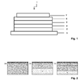
- Fig. 1 depicts a simplified schematic illustration of an optoelectronic device according to the present invention.
- the optoelectronic device 1 is a solar cell and comprises a first electrode 2 (ITO), which is arranged on a substrate 3 (glass).
- a hole transport layer (HTL) 4 is deposited on the first electrode 2 .
- the hole transport layer (HTL) 4 comprises CH 3 NH 3 PblX 3 doped with F4-TCNQ.
- an active layer 5 is deposited on the hole transport layer (HTL) 4 deposited.
- the active layer 5 comprises an undoped pervoskite, e.g. CH 3 NH 3 PblX 3 .
- an electron transport layer 6 is deposited.
- the electron transport layer (ETL) 6 comprises C60.
- the second electrode comprises at least a metal, wherein the metal is selected from Al, Ag, Au, Ti, Pt, Cr, Zn, Sn, Sr, In, Sc, Hf or a mixture thereof.
- the optoelectronic device 1 is made in accordance to the aforementioned embodiment except that the hole transport layer (HTL) 4 comprises CH 3 NH 3 Pbl(I,Cl) 3 doped with F6-TCNNQ.
- HTL hole transport layer
- the optoelectronic device 1 comprises a first electrode 2 (ITO), which is arranged on a substrate 3 (glass).
- a hole transport layer (HTL) 4 is deposited on the first electrode 2 .
- the hole transport layer (HTL) 4 comprises Spiro-MeO-TAD.
- an active layer 5 is deposited on the hole transport layer (HTL) 4 .
- the active layer 5 comprises an undoped pervoskite, e.g. CH 3 NH 3 PbX 3 .
- an electron transport layer 6 is deposited.
- the electron transport layer (ETL) 6 comprises CH 3 NH 3 PbX 3 doped with W 2 (hpp) 4 .
- a second electrode deposited, wherein the second electrode comprises at least a metal, e.g. Ag.
- the optoelectronic device 1 is made in accordance to the aforementioned embodiment except that the electron transport layer (ETL) 6 comprises CH 3 NH 3 PbX 3 doped with Cr 2 (hpp) 4 .
- ETL electron transport layer
- the optoelectronic device 1 comprises a first electrode 2 (ITO), which is arranged on a substrate 3 (glass).
- a hole transport layer (HTL) 4 is deposited on the first electrode 2 .
- the hole transport layer (HTL) 4 comprises p-doped perovskite.
- an active layer 5 is deposited on the hole transport layer (HTL) 4 .
- the active layer 5 comprises an undoped pervoskite, e.g. CH 3 NH 3 PbX 3 .
- an electron transport layer 6 is deposited.
- the electron transport layer (ETL) 6 comprises n-doped CH 3 NH 3 PbX 3 .
- a second electrode deposited wherein the second electrode comprises at least a metal, e.g . Ag.
- the manufacturing of the optoeletronic device is performed by a thermal evaporation under vacuum conditions.
- Thin film samples are prepared by thermal vapor deposition in ultra-high vacuum (UHV) with a base pressure at or below 10 -7 mbar.
- UHV ultra-high vacuum
- the layers in a multi layer device are deposited sequentially and their thicknesses are determined during evaporation using quartz crystal monitors calibrated for the respective material prior to evaporation.
- a typical layer structure of substrate, electrode, charge injection layer and charge carrier transport layer or a layout as an optoelectronic device (1) according to the invention as depicted in Fig. 1 comprises independently on the intended purpose Optoelectronic device (1), First electrode or anode (2), Substrate (3), Hole transport layer (4), Active layer (5), Electron transport layer (6), Second electrode or cathode (7), optionally one or more charge injection layer (8) or buffer layer to compensate for unevenness of the electrode, optionally one or more charge blocking layer (9), encapsulation (10), but can be customized for each application.
- all layers are deposited by thermal evaporation in an ultra-high vacuum chamber and/or applied by coating from solution.
- the production of a multilayer organic structure by coating from solution requires that the solvent is incompatible with the respective preceding layer to solve this not to swell again, or even destroy.
Landscapes
- Engineering & Computer Science (AREA)
- Physics & Mathematics (AREA)
- Chemical & Material Sciences (AREA)
- Materials Engineering (AREA)
- Electromagnetism (AREA)
- Optics & Photonics (AREA)
- Manufacturing & Machinery (AREA)
- Photovoltaic Devices (AREA)
Priority Applications (2)
| Application Number | Priority Date | Filing Date | Title |
|---|---|---|---|
| EP15167145.0A EP2942826B1 (de) | 2014-05-09 | 2015-05-11 | Dotierte perovskite und deren verwendung als aktive und/oder ladungstransportschichten in optoelektronischen vorrichtungen |
| EP17154988.4A EP3185323A1 (de) | 2014-05-09 | 2015-05-11 | Dotierte perovskite und deren verwendung als aktive und/oder ladungstransportschichten in optoelektronischen vorrichtungen |
Applications Claiming Priority (2)
| Application Number | Priority Date | Filing Date | Title |
|---|---|---|---|
| EP14001735 | 2014-05-09 | ||
| EP15167145.0A EP2942826B1 (de) | 2014-05-09 | 2015-05-11 | Dotierte perovskite und deren verwendung als aktive und/oder ladungstransportschichten in optoelektronischen vorrichtungen |
Related Child Applications (2)
| Application Number | Title | Priority Date | Filing Date |
|---|---|---|---|
| EP17154988.4A Division EP3185323A1 (de) | 2014-05-09 | 2015-05-11 | Dotierte perovskite und deren verwendung als aktive und/oder ladungstransportschichten in optoelektronischen vorrichtungen |
| EP17154988.4A Division-Into EP3185323A1 (de) | 2014-05-09 | 2015-05-11 | Dotierte perovskite und deren verwendung als aktive und/oder ladungstransportschichten in optoelektronischen vorrichtungen |
Publications (3)
| Publication Number | Publication Date |
|---|---|
| EP2942826A2 true EP2942826A2 (de) | 2015-11-11 |
| EP2942826A3 EP2942826A3 (de) | 2016-02-24 |
| EP2942826B1 EP2942826B1 (de) | 2023-03-01 |
Family
ID=50771028
Family Applications (2)
| Application Number | Title | Priority Date | Filing Date |
|---|---|---|---|
| EP15167145.0A Active EP2942826B1 (de) | 2014-05-09 | 2015-05-11 | Dotierte perovskite und deren verwendung als aktive und/oder ladungstransportschichten in optoelektronischen vorrichtungen |
| EP17154988.4A Pending EP3185323A1 (de) | 2014-05-09 | 2015-05-11 | Dotierte perovskite und deren verwendung als aktive und/oder ladungstransportschichten in optoelektronischen vorrichtungen |
Family Applications After (1)
| Application Number | Title | Priority Date | Filing Date |
|---|---|---|---|
| EP17154988.4A Pending EP3185323A1 (de) | 2014-05-09 | 2015-05-11 | Dotierte perovskite und deren verwendung als aktive und/oder ladungstransportschichten in optoelektronischen vorrichtungen |
Country Status (1)
| Country | Link |
|---|---|
| EP (2) | EP2942826B1 (de) |
Cited By (25)
| Publication number | Priority date | Publication date | Assignee | Title |
|---|---|---|---|---|
| CN105405974A (zh) * | 2015-11-17 | 2016-03-16 | 华中科技大学 | 一种p型掺杂的钙钛矿光电功能材料及其应用 |
| DE102015225145A1 (de) | 2015-12-14 | 2017-06-14 | Siemens Healthcare Gmbh | Perowskitpartikel für die Herstellung von Röntgendetektoren mittels Abscheidung aus der Trockenphase |
| JP2017126677A (ja) * | 2016-01-14 | 2017-07-20 | 住友化学株式会社 | 光電変換素子 |
| JP2017126676A (ja) * | 2016-01-14 | 2017-07-20 | 住友化学株式会社 | 光電変換素子 |
| WO2017135705A1 (ko) * | 2016-02-03 | 2017-08-10 | 주식회사 엘지화학 | 유무기 하이브리드 페로브스카이트 태양 전지 |
| EP3242340A1 (de) | 2016-05-04 | 2017-11-08 | Novaled GmbH | Solarzelle |
| CN107425121A (zh) * | 2016-05-24 | 2017-12-01 | 中国科学院苏州纳米技术与纳米仿生研究所 | 钙钛矿薄膜太阳能电池及其制备方法 |
| CN107851720A (zh) * | 2016-07-14 | 2018-03-27 | 株式会社Lg化学 | 有机‑无机混合太阳能电池 |
| JP2018085497A (ja) * | 2016-11-16 | 2018-05-31 | ペクセル・テクノロジーズ株式会社 | 光電変換素子 |
| US20180151812A1 (en) * | 2016-04-15 | 2018-05-31 | Shenzhen China Star Optoelectronics Technology Co. Ltd. | OLED DISPLAY DEVICE and MANUFACTURING METHOD THEREOF |
| US20180269235A1 (en) * | 2017-03-17 | 2018-09-20 | Samsung Electronics Co., Ltd. | Photoelectric conversion device including perovskite compound, method of manufacturing the same, and imaging device including the same |
| CN110112305A (zh) * | 2019-05-24 | 2019-08-09 | 京东方科技集团股份有限公司 | Qled器件及其制作方法、显示面板及显示装置 |
| US20190326065A1 (en) * | 2018-04-24 | 2019-10-24 | Nutech Ventures | Molecular doping enabled scalable blading of efficient hole transport layer-free perovskite solar cells |
| WO2019232408A1 (en) * | 2018-06-01 | 2019-12-05 | The University Of North Carolina At Chapel Hill | Doped polycrystalline perovskite films with extended charge carrier recombination lifetimes and high power conversion efficiencies |
| CN111463349A (zh) * | 2019-06-29 | 2020-07-28 | 杭州纤纳光电科技有限公司 | 一种提高钙钛矿太阳能电池稳定性的方法 |
| US10784449B2 (en) | 2016-04-11 | 2020-09-22 | Samsung Display Co., Ltd. | Perovskite compound, thin layer comprising the perovskite compound, and optoelectronic device comprising the perovskite compound |
| US10797250B2 (en) | 2018-02-26 | 2020-10-06 | Samsung Display Co., Ltd. | Electronic apparatus and lighting apparatus |
| US10978650B2 (en) | 2016-06-02 | 2021-04-13 | Samsung Display Co., Ltd. | Light-emitting device |
| CN114005943A (zh) * | 2021-12-03 | 2022-02-01 | 华能新能源股份有限公司 | 一种双面受光的钙钛矿太阳能光伏组件及其制备方法 |
| CN114171683A (zh) * | 2021-12-03 | 2022-03-11 | 华能新能源股份有限公司 | 一种钙钛矿太阳能电池及其制备方法 |
| JP2022132578A (ja) * | 2018-07-18 | 2022-09-08 | 三菱ケミカル株式会社 | 光電変換素子及び太陽電池モジュール |
| WO2023010746A1 (zh) * | 2021-08-05 | 2023-02-09 | 中国科学院深圳先进技术研究院 | n-i结构钙钛矿基X光探测器及其制备方法 |
| EP4292144A1 (de) * | 2021-02-12 | 2023-12-20 | First Solar, Inc. | Materialien und verfahren für lochtransportschichten in perowskit-fotovoltaikvorrichtungen |
| US11895855B2 (en) | 2019-08-29 | 2024-02-06 | Samsung Electronics Co., Ltd. | Light-emitting device |
| JP2024521193A (ja) * | 2021-09-29 | 2024-05-28 | シャンラオ シンユエン ユエドン テクノロジー デベロップメント シーオー.,エルティーディー | 太陽電池及びその製造方法 |
Family Cites Families (6)
| Publication number | Priority date | Publication date | Assignee | Title |
|---|---|---|---|---|
| WO2007109734A2 (en) * | 2006-03-21 | 2007-09-27 | Ultradots, Inc. | Luminescent materials that emit light in the visible range or the near infrared range |
| KR20140007045A (ko) * | 2012-07-05 | 2014-01-16 | 한국화학연구원 | 나노구조 유-무기 하이브리드 태양전지 |
| EP2693503A1 (de) * | 2012-08-03 | 2014-02-05 | Ecole Polytechnique Fédérale de Lausanne (EPFL) | Organometallische Halid-Perovskit-Heteroverbindungssolarzelle und Herstellung davon |
| EP3058595A4 (de) * | 2013-10-16 | 2017-03-08 | Omnipv, Inc. | Photovoltaikzellen mit halidmaterialien |
| CN104201285A (zh) * | 2014-09-03 | 2014-12-10 | 北京大学 | 空穴传输体系不含有离子添加剂的钙钛矿太阳能电池 |
| US10115918B2 (en) * | 2014-11-05 | 2018-10-30 | Okinawa Institute Of Science And Technology School Corporation | Doping engineered hole transport layer for perovskite-based device |
-
2015
- 2015-05-11 EP EP15167145.0A patent/EP2942826B1/de active Active
- 2015-05-11 EP EP17154988.4A patent/EP3185323A1/de active Pending
Non-Patent Citations (8)
| Title |
|---|
| "New ion continues perovskite solar's flat-out progress Press Release", KRICT, 2015 |
| GRATZEI, M.: "The light and shade of perovskite solar cells", NAT MATER, vol. 13, 2014, pages 838 - 842 |
| HODES, G.: "Perovskite-Based Solar Cells", SCIENCE, vol. 342, no. 6156, 2013, pages 317 - 318 |
| LIU, M. ET AL.: "Efficient planar heterojunction perovskite solar cells by vapor deposition", NATURE, vol. 501, 2013, pages 395 - 398 |
| MALINKIEWICZ, O. ET AL.: "Perovskite solar cells employing organic charge-transport layers", NAT PHOTON, vol. 8, 2014, pages 128 - 132 |
| PEUMANN ET AL., J. APPL. PHYS., vol. 93, no. 7, 2003, pages 3693 - 3722 |
| WALZER ET AL., CHEMICAL REVIEWS, vol. 107, no. 4, 2007, pages 1233 - 1271 |
| WALZER, K. ET AL.: "Highly efficient organic devices based on electrically doped transport layers", CHEM. REV., vol. 107, 2007, pages 1233 - 1271 |
Cited By (38)
| Publication number | Priority date | Publication date | Assignee | Title |
|---|---|---|---|---|
| CN105405974A (zh) * | 2015-11-17 | 2016-03-16 | 华中科技大学 | 一种p型掺杂的钙钛矿光电功能材料及其应用 |
| DE102015225145A1 (de) | 2015-12-14 | 2017-06-14 | Siemens Healthcare Gmbh | Perowskitpartikel für die Herstellung von Röntgendetektoren mittels Abscheidung aus der Trockenphase |
| US10340465B2 (en) | 2015-12-14 | 2019-07-02 | Siemens Healthcare Gmbh | Perovskite particles for producing X-ray detectors by means of deposition from the dry phase |
| JP2017126677A (ja) * | 2016-01-14 | 2017-07-20 | 住友化学株式会社 | 光電変換素子 |
| JP2017126676A (ja) * | 2016-01-14 | 2017-07-20 | 住友化学株式会社 | 光電変換素子 |
| WO2017135705A1 (ko) * | 2016-02-03 | 2017-08-10 | 주식회사 엘지화학 | 유무기 하이브리드 페로브스카이트 태양 전지 |
| US10784449B2 (en) | 2016-04-11 | 2020-09-22 | Samsung Display Co., Ltd. | Perovskite compound, thin layer comprising the perovskite compound, and optoelectronic device comprising the perovskite compound |
| US20180151812A1 (en) * | 2016-04-15 | 2018-05-31 | Shenzhen China Star Optoelectronics Technology Co. Ltd. | OLED DISPLAY DEVICE and MANUFACTURING METHOD THEREOF |
| WO2017191265A1 (en) | 2016-05-04 | 2017-11-09 | Novaled Gmbh | Solar cell |
| EP3242340A1 (de) | 2016-05-04 | 2017-11-08 | Novaled GmbH | Solarzelle |
| CN107425121B (zh) * | 2016-05-24 | 2020-11-27 | 中国科学院苏州纳米技术与纳米仿生研究所 | 钙钛矿薄膜太阳能电池及其制备方法 |
| CN107425121A (zh) * | 2016-05-24 | 2017-12-01 | 中国科学院苏州纳米技术与纳米仿生研究所 | 钙钛矿薄膜太阳能电池及其制备方法 |
| US10978650B2 (en) | 2016-06-02 | 2021-04-13 | Samsung Display Co., Ltd. | Light-emitting device |
| CN107851720A (zh) * | 2016-07-14 | 2018-03-27 | 株式会社Lg化学 | 有机‑无机混合太阳能电池 |
| CN107851720B (zh) * | 2016-07-14 | 2020-08-21 | 株式会社Lg化学 | 有机-无机混合太阳能电池 |
| JP2018085497A (ja) * | 2016-11-16 | 2018-05-31 | ペクセル・テクノロジーズ株式会社 | 光電変換素子 |
| JP2018157204A (ja) * | 2017-03-17 | 2018-10-04 | 三星電子株式会社Samsung Electronics Co.,Ltd. | ペロブスカイト化合物を含む光電変換素子、その製造方法、およびそれを含む撮像装置 |
| US11728353B2 (en) | 2017-03-17 | 2023-08-15 | Samsung Electronics Co., Ltd. | Photoelectric conversion device including perovskite compound, method of manufacturing the same, and imaging device including the same |
| CN108630816B (zh) * | 2017-03-17 | 2022-12-09 | 三星电子株式会社 | 包括钙钛矿化合物的光电转换器件、其制造方法以及包括其的成像装置 |
| CN108630816A (zh) * | 2017-03-17 | 2018-10-09 | 三星电子株式会社 | 包括钙钛矿化合物的光电转换器件、其制造方法以及包括其的成像装置 |
| EP3379592A1 (de) * | 2017-03-17 | 2018-09-26 | Samsung Electronics Co., Ltd. | Umwandlungsvorrichtung mit perowskitverbindung, verfahren zur herstellung davon und bildgebungsvorrichtung damit |
| US20180269235A1 (en) * | 2017-03-17 | 2018-09-20 | Samsung Electronics Co., Ltd. | Photoelectric conversion device including perovskite compound, method of manufacturing the same, and imaging device including the same |
| US10903252B2 (en) | 2017-03-17 | 2021-01-26 | Samsung Electronics Co., Ltd. | Photoelectric conversion device including perovskite compound, method of manufacturing the same, and imaging device including the same |
| US10797250B2 (en) | 2018-02-26 | 2020-10-06 | Samsung Display Co., Ltd. | Electronic apparatus and lighting apparatus |
| US20190326065A1 (en) * | 2018-04-24 | 2019-10-24 | Nutech Ventures | Molecular doping enabled scalable blading of efficient hole transport layer-free perovskite solar cells |
| WO2019232408A1 (en) * | 2018-06-01 | 2019-12-05 | The University Of North Carolina At Chapel Hill | Doped polycrystalline perovskite films with extended charge carrier recombination lifetimes and high power conversion efficiencies |
| JP2022132578A (ja) * | 2018-07-18 | 2022-09-08 | 三菱ケミカル株式会社 | 光電変換素子及び太陽電池モジュール |
| JP7261372B2 (ja) | 2018-07-18 | 2023-04-20 | 三菱ケミカル株式会社 | 光電変換素子及び太陽電池モジュール |
| CN110112305B (zh) * | 2019-05-24 | 2023-04-07 | 京东方科技集团股份有限公司 | Qled器件及其制作方法、显示面板及显示装置 |
| CN110112305A (zh) * | 2019-05-24 | 2019-08-09 | 京东方科技集团股份有限公司 | Qled器件及其制作方法、显示面板及显示装置 |
| CN111463349A (zh) * | 2019-06-29 | 2020-07-28 | 杭州纤纳光电科技有限公司 | 一种提高钙钛矿太阳能电池稳定性的方法 |
| US11895855B2 (en) | 2019-08-29 | 2024-02-06 | Samsung Electronics Co., Ltd. | Light-emitting device |
| EP4292144A1 (de) * | 2021-02-12 | 2023-12-20 | First Solar, Inc. | Materialien und verfahren für lochtransportschichten in perowskit-fotovoltaikvorrichtungen |
| EP4292144B1 (de) * | 2021-02-12 | 2026-01-21 | First Solar, Inc. | Materialien und verfahren für lochtransportschichten in perowskit-fotovoltaikvorrichtungen |
| WO2023010746A1 (zh) * | 2021-08-05 | 2023-02-09 | 中国科学院深圳先进技术研究院 | n-i结构钙钛矿基X光探测器及其制备方法 |
| JP2024521193A (ja) * | 2021-09-29 | 2024-05-28 | シャンラオ シンユエン ユエドン テクノロジー デベロップメント シーオー.,エルティーディー | 太陽電池及びその製造方法 |
| CN114005943A (zh) * | 2021-12-03 | 2022-02-01 | 华能新能源股份有限公司 | 一种双面受光的钙钛矿太阳能光伏组件及其制备方法 |
| CN114171683A (zh) * | 2021-12-03 | 2022-03-11 | 华能新能源股份有限公司 | 一种钙钛矿太阳能电池及其制备方法 |
Also Published As
| Publication number | Publication date |
|---|---|
| EP3185323A1 (de) | 2017-06-28 |
| EP2942826A3 (de) | 2016-02-24 |
| EP2942826B1 (de) | 2023-03-01 |
Similar Documents
| Publication | Publication Date | Title |
|---|---|---|
| EP2942826B1 (de) | Dotierte perovskite und deren verwendung als aktive und/oder ladungstransportschichten in optoelektronischen vorrichtungen | |
| Ran et al. | Bilateral interface engineering toward efficient 2D–3D bulk heterojunction tin halide lead-free perovskite solar cells | |
| KR101717430B1 (ko) | 페로브스카이트 기반 태양전지 | |
| KR102519361B1 (ko) | 페로브스카이트 태양 전지 물질의 제조 방법 | |
| JP6374134B1 (ja) | ペロブスカイト材料層プロセシング | |
| CA2968367C (en) | Bi-and tri-layer interfacial layers in perovskite material devices | |
| US11211559B2 (en) | Materials for controlling the epitaxial growth of photoactive layers in photovoltaic devices | |
| US9431621B2 (en) | Metal oxide charge transport material doped with organic molecules | |
| EP4322235A1 (de) | Perowskit-solarzelle und tandemsolarzelle damit | |
| US20120125419A1 (en) | Photoactive component comprising an inverted layer sequence, and method for the production of said component | |
| EP3242340B1 (de) | Solarzelle | |
| US10636580B2 (en) | Organic-inorganic hybrid solar cell | |
| Avila et al. | Influence of doped charge transport layers on efficient perovskite solar cells | |
| KR102008737B1 (ko) | 페로브스카이트 물질 디바이스에서의 티타네이트 계면 층 | |
| Sharma et al. | Comparative study of hole transporting layers commonly used in high-efficiency perovskite solar cells | |
| US20230167326A1 (en) | Methods for Forming Perovskite Material Layers | |
| Kumar et al. | Fusible low work function top electrode for vacuum-free perovskite light-emitting diode application: Role of OH-terminated sn atoms at the alloy surface | |
| EP2659529B2 (de) | Optoelektronisches bauelement mit dotierten schichten | |
| EP4181223A1 (de) | Mit säurebasiertem nebenprodukt dotiertes organisches lochtransportmaterial und optische vorrichtung damit | |
| Bhaumik et al. | A perspective on perovskite solar cells | |
| KR102825228B1 (ko) | 표면처리층을 포함하는 페로브스카이트 광소자 및 그 제조 방법 |
Legal Events
| Date | Code | Title | Description |
|---|---|---|---|
| PUAI | Public reference made under article 153(3) epc to a published international application that has entered the european phase |
Free format text: ORIGINAL CODE: 0009012 |
|
| AK | Designated contracting states |
Kind code of ref document: A2 Designated state(s): AL AT BE BG CH CY CZ DE DK EE ES FI FR GB GR HR HU IE IS IT LI LT LU LV MC MK MT NL NO PL PT RO RS SE SI SK SM TR |
|
| AX | Request for extension of the european patent |
Extension state: BA ME |
|
| PUAL | Search report despatched |
Free format text: ORIGINAL CODE: 0009013 |
|
| AK | Designated contracting states |
Kind code of ref document: A3 Designated state(s): AL AT BE BG CH CY CZ DE DK EE ES FI FR GB GR HR HU IE IS IT LI LT LU LV MC MK MT NL NO PL PT RO RS SE SI SK SM TR |
|
| AX | Request for extension of the european patent |
Extension state: BA ME |
|
| RIC1 | Information provided on ipc code assigned before grant |
Ipc: H01L 51/44 20060101ALI20160115BHEP Ipc: H01L 51/42 20060101AFI20160115BHEP Ipc: H01L 51/50 20060101ALI20160115BHEP |
|
| 17P | Request for examination filed |
Effective date: 20160824 |
|
| RBV | Designated contracting states (corrected) |
Designated state(s): AL AT BE BG CH CY CZ DE DK EE ES FI FR GB GR HR HU IE IS IT LI LT LU LV MC MK MT NL NO PL PT RO RS SE SI SK SM TR |
|
| RAP1 | Party data changed (applicant data changed or rights of an application transferred) |
Owner name: NOVALED GMBH |
|
| RAP1 | Party data changed (applicant data changed or rights of an application transferred) |
Owner name: NOVALED GMBH |
|
| STAA | Information on the status of an ep patent application or granted ep patent |
Free format text: STATUS: EXAMINATION IS IN PROGRESS |
|
| 17Q | First examination report despatched |
Effective date: 20190823 |
|
| GRAP | Despatch of communication of intention to grant a patent |
Free format text: ORIGINAL CODE: EPIDOSNIGR1 |
|
| STAA | Information on the status of an ep patent application or granted ep patent |
Free format text: STATUS: GRANT OF PATENT IS INTENDED |
|
| INTG | Intention to grant announced |
Effective date: 20221007 |
|
| RIN1 | Information on inventor provided before grant (corrected) |
Inventor name: LEO, KARL Inventor name: KOERNER, CHRISTIAN Inventor name: POLANDER, LAUREN |
|
| GRAS | Grant fee paid |
Free format text: ORIGINAL CODE: EPIDOSNIGR3 |
|
| GRAA | (expected) grant |
Free format text: ORIGINAL CODE: 0009210 |
|
| STAA | Information on the status of an ep patent application or granted ep patent |
Free format text: STATUS: THE PATENT HAS BEEN GRANTED |
|
| AK | Designated contracting states |
Kind code of ref document: B1 Designated state(s): AL AT BE BG CH CY CZ DE DK EE ES FI FR GB GR HR HU IE IS IT LI LT LU LV MC MK MT NL NO PL PT RO RS SE SI SK SM TR |
|
| REG | Reference to a national code |
Ref country code: GB Ref legal event code: FG4D |
|
| REG | Reference to a national code |
Ref country code: CH Ref legal event code: EP Ref country code: AT Ref legal event code: REF Ref document number: 1551608 Country of ref document: AT Kind code of ref document: T Effective date: 20230315 |
|
| REG | Reference to a national code |
Ref country code: DE Ref legal event code: R096 Ref document number: 602015082627 Country of ref document: DE |
|
| REG | Reference to a national code |
Ref country code: IE Ref legal event code: FG4D |
|
| P01 | Opt-out of the competence of the unified patent court (upc) registered |
Effective date: 20230515 |
|
| REG | Reference to a national code |
Ref country code: LT Ref legal event code: MG9D |
|
| REG | Reference to a national code |
Ref country code: NL Ref legal event code: MP Effective date: 20230301 |
|
| PG25 | Lapsed in a contracting state [announced via postgrant information from national office to epo] |
Ref country code: RS Free format text: LAPSE BECAUSE OF FAILURE TO SUBMIT A TRANSLATION OF THE DESCRIPTION OR TO PAY THE FEE WITHIN THE PRESCRIBED TIME-LIMIT Effective date: 20230301 Ref country code: NO Free format text: LAPSE BECAUSE OF FAILURE TO SUBMIT A TRANSLATION OF THE DESCRIPTION OR TO PAY THE FEE WITHIN THE PRESCRIBED TIME-LIMIT Effective date: 20230601 Ref country code: LV Free format text: LAPSE BECAUSE OF FAILURE TO SUBMIT A TRANSLATION OF THE DESCRIPTION OR TO PAY THE FEE WITHIN THE PRESCRIBED TIME-LIMIT Effective date: 20230301 Ref country code: LT Free format text: LAPSE BECAUSE OF FAILURE TO SUBMIT A TRANSLATION OF THE DESCRIPTION OR TO PAY THE FEE WITHIN THE PRESCRIBED TIME-LIMIT Effective date: 20230301 Ref country code: HR Free format text: LAPSE BECAUSE OF FAILURE TO SUBMIT A TRANSLATION OF THE DESCRIPTION OR TO PAY THE FEE WITHIN THE PRESCRIBED TIME-LIMIT Effective date: 20230301 Ref country code: ES Free format text: LAPSE BECAUSE OF FAILURE TO SUBMIT A TRANSLATION OF THE DESCRIPTION OR TO PAY THE FEE WITHIN THE PRESCRIBED TIME-LIMIT Effective date: 20230301 |
|
| REG | Reference to a national code |
Ref country code: AT Ref legal event code: MK05 Ref document number: 1551608 Country of ref document: AT Kind code of ref document: T Effective date: 20230301 |
|
| PG25 | Lapsed in a contracting state [announced via postgrant information from national office to epo] |
Ref country code: SE Free format text: LAPSE BECAUSE OF FAILURE TO SUBMIT A TRANSLATION OF THE DESCRIPTION OR TO PAY THE FEE WITHIN THE PRESCRIBED TIME-LIMIT Effective date: 20230301 Ref country code: PL Free format text: LAPSE BECAUSE OF FAILURE TO SUBMIT A TRANSLATION OF THE DESCRIPTION OR TO PAY THE FEE WITHIN THE PRESCRIBED TIME-LIMIT Effective date: 20230301 Ref country code: NL Free format text: LAPSE BECAUSE OF FAILURE TO SUBMIT A TRANSLATION OF THE DESCRIPTION OR TO PAY THE FEE WITHIN THE PRESCRIBED TIME-LIMIT Effective date: 20230301 Ref country code: GR Free format text: LAPSE BECAUSE OF FAILURE TO SUBMIT A TRANSLATION OF THE DESCRIPTION OR TO PAY THE FEE WITHIN THE PRESCRIBED TIME-LIMIT Effective date: 20230602 Ref country code: FI Free format text: LAPSE BECAUSE OF FAILURE TO SUBMIT A TRANSLATION OF THE DESCRIPTION OR TO PAY THE FEE WITHIN THE PRESCRIBED TIME-LIMIT Effective date: 20230301 |
|
| PG25 | Lapsed in a contracting state [announced via postgrant information from national office to epo] |
Ref country code: SM Free format text: LAPSE BECAUSE OF FAILURE TO SUBMIT A TRANSLATION OF THE DESCRIPTION OR TO PAY THE FEE WITHIN THE PRESCRIBED TIME-LIMIT Effective date: 20230301 Ref country code: RO Free format text: LAPSE BECAUSE OF FAILURE TO SUBMIT A TRANSLATION OF THE DESCRIPTION OR TO PAY THE FEE WITHIN THE PRESCRIBED TIME-LIMIT Effective date: 20230301 Ref country code: PT Free format text: LAPSE BECAUSE OF FAILURE TO SUBMIT A TRANSLATION OF THE DESCRIPTION OR TO PAY THE FEE WITHIN THE PRESCRIBED TIME-LIMIT Effective date: 20230703 Ref country code: EE Free format text: LAPSE BECAUSE OF FAILURE TO SUBMIT A TRANSLATION OF THE DESCRIPTION OR TO PAY THE FEE WITHIN THE PRESCRIBED TIME-LIMIT Effective date: 20230301 Ref country code: CZ Free format text: LAPSE BECAUSE OF FAILURE TO SUBMIT A TRANSLATION OF THE DESCRIPTION OR TO PAY THE FEE WITHIN THE PRESCRIBED TIME-LIMIT Effective date: 20230301 Ref country code: AT Free format text: LAPSE BECAUSE OF FAILURE TO SUBMIT A TRANSLATION OF THE DESCRIPTION OR TO PAY THE FEE WITHIN THE PRESCRIBED TIME-LIMIT Effective date: 20230301 |
|
| PG25 | Lapsed in a contracting state [announced via postgrant information from national office to epo] |
Ref country code: SK Free format text: LAPSE BECAUSE OF FAILURE TO SUBMIT A TRANSLATION OF THE DESCRIPTION OR TO PAY THE FEE WITHIN THE PRESCRIBED TIME-LIMIT Effective date: 20230301 Ref country code: IS Free format text: LAPSE BECAUSE OF FAILURE TO SUBMIT A TRANSLATION OF THE DESCRIPTION OR TO PAY THE FEE WITHIN THE PRESCRIBED TIME-LIMIT Effective date: 20230701 |
|
| REG | Reference to a national code |
Ref country code: DE Ref legal event code: R097 Ref document number: 602015082627 Country of ref document: DE |
|
| REG | Reference to a national code |
Ref country code: CH Ref legal event code: PL |
|
| PLBE | No opposition filed within time limit |
Free format text: ORIGINAL CODE: 0009261 |
|
| STAA | Information on the status of an ep patent application or granted ep patent |
Free format text: STATUS: NO OPPOSITION FILED WITHIN TIME LIMIT |
|
| PG25 | Lapsed in a contracting state [announced via postgrant information from national office to epo] |
Ref country code: MC Free format text: LAPSE BECAUSE OF FAILURE TO SUBMIT A TRANSLATION OF THE DESCRIPTION OR TO PAY THE FEE WITHIN THE PRESCRIBED TIME-LIMIT Effective date: 20230301 |
|
| REG | Reference to a national code |
Ref country code: BE Ref legal event code: MM Effective date: 20230531 |
|
| PG25 | Lapsed in a contracting state [announced via postgrant information from national office to epo] |
Ref country code: SI Free format text: LAPSE BECAUSE OF FAILURE TO SUBMIT A TRANSLATION OF THE DESCRIPTION OR TO PAY THE FEE WITHIN THE PRESCRIBED TIME-LIMIT Effective date: 20230301 Ref country code: MC Free format text: LAPSE BECAUSE OF FAILURE TO SUBMIT A TRANSLATION OF THE DESCRIPTION OR TO PAY THE FEE WITHIN THE PRESCRIBED TIME-LIMIT Effective date: 20230301 Ref country code: LU Free format text: LAPSE BECAUSE OF NON-PAYMENT OF DUE FEES Effective date: 20230511 Ref country code: LI Free format text: LAPSE BECAUSE OF NON-PAYMENT OF DUE FEES Effective date: 20230531 Ref country code: DK Free format text: LAPSE BECAUSE OF FAILURE TO SUBMIT A TRANSLATION OF THE DESCRIPTION OR TO PAY THE FEE WITHIN THE PRESCRIBED TIME-LIMIT Effective date: 20230301 Ref country code: CH Free format text: LAPSE BECAUSE OF NON-PAYMENT OF DUE FEES Effective date: 20230531 |
|
| 26N | No opposition filed |
Effective date: 20231204 |
|
| GBPC | Gb: european patent ceased through non-payment of renewal fee |
Effective date: 20230601 |
|
| REG | Reference to a national code |
Ref country code: IE Ref legal event code: MM4A |
|
| PG25 | Lapsed in a contracting state [announced via postgrant information from national office to epo] |
Ref country code: IE Free format text: LAPSE BECAUSE OF NON-PAYMENT OF DUE FEES Effective date: 20230511 |
|
| PG25 | Lapsed in a contracting state [announced via postgrant information from national office to epo] |
Ref country code: IE Free format text: LAPSE BECAUSE OF NON-PAYMENT OF DUE FEES Effective date: 20230511 Ref country code: GB Free format text: LAPSE BECAUSE OF NON-PAYMENT OF DUE FEES Effective date: 20230601 |
|
| PG25 | Lapsed in a contracting state [announced via postgrant information from national office to epo] |
Ref country code: IT Free format text: LAPSE BECAUSE OF FAILURE TO SUBMIT A TRANSLATION OF THE DESCRIPTION OR TO PAY THE FEE WITHIN THE PRESCRIBED TIME-LIMIT Effective date: 20230301 Ref country code: FR Free format text: LAPSE BECAUSE OF NON-PAYMENT OF DUE FEES Effective date: 20230531 Ref country code: BE Free format text: LAPSE BECAUSE OF NON-PAYMENT OF DUE FEES Effective date: 20230531 |
|
| PG25 | Lapsed in a contracting state [announced via postgrant information from national office to epo] |
Ref country code: BG Free format text: LAPSE BECAUSE OF FAILURE TO SUBMIT A TRANSLATION OF THE DESCRIPTION OR TO PAY THE FEE WITHIN THE PRESCRIBED TIME-LIMIT Effective date: 20230301 |
|
| PG25 | Lapsed in a contracting state [announced via postgrant information from national office to epo] |
Ref country code: BG Free format text: LAPSE BECAUSE OF FAILURE TO SUBMIT A TRANSLATION OF THE DESCRIPTION OR TO PAY THE FEE WITHIN THE PRESCRIBED TIME-LIMIT Effective date: 20230301 |
|
| PGFP | Annual fee paid to national office [announced via postgrant information from national office to epo] |
Ref country code: DE Payment date: 20250319 Year of fee payment: 11 |
|
| PG25 | Lapsed in a contracting state [announced via postgrant information from national office to epo] |
Ref country code: CY Free format text: LAPSE BECAUSE OF FAILURE TO SUBMIT A TRANSLATION OF THE DESCRIPTION OR TO PAY THE FEE WITHIN THE PRESCRIBED TIME-LIMIT; INVALID AB INITIO Effective date: 20150511 |
|
| PG25 | Lapsed in a contracting state [announced via postgrant information from national office to epo] |
Ref country code: HU Free format text: LAPSE BECAUSE OF FAILURE TO SUBMIT A TRANSLATION OF THE DESCRIPTION OR TO PAY THE FEE WITHIN THE PRESCRIBED TIME-LIMIT; INVALID AB INITIO Effective date: 20150511 |
|
| PG25 | Lapsed in a contracting state [announced via postgrant information from national office to epo] |
Ref country code: TR Free format text: LAPSE BECAUSE OF FAILURE TO SUBMIT A TRANSLATION OF THE DESCRIPTION OR TO PAY THE FEE WITHIN THE PRESCRIBED TIME-LIMIT Effective date: 20230301 |