EP2944967B1 - Élément d'adaptation d'impédance pour la tension et/ou les dispositifs de détection de courant - Google Patents
Élément d'adaptation d'impédance pour la tension et/ou les dispositifs de détection de courant Download PDFInfo
- Publication number
- EP2944967B1 EP2944967B1 EP14001713.8A EP14001713A EP2944967B1 EP 2944967 B1 EP2944967 B1 EP 2944967B1 EP 14001713 A EP14001713 A EP 14001713A EP 2944967 B1 EP2944967 B1 EP 2944967B1
- Authority
- EP
- European Patent Office
- Prior art keywords
- impedance matching
- sensing device
- current
- matching element
- voltage sensing
- Prior art date
- Legal status (The legal status is an assumption and is not a legal conclusion. Google has not performed a legal analysis and makes no representation as to the accuracy of the status listed.)
- Not-in-force
Links
Images



Classifications
-
- H—ELECTRICITY
- H03—ELECTRONIC CIRCUITRY
- H03H—IMPEDANCE NETWORKS, e.g. RESONANT CIRCUITS; RESONATORS
- H03H7/00—Multiple-port networks comprising only passive electrical elements as network components
- H03H7/38—Impedance-matching networks
-
- G—PHYSICS
- G01—MEASURING; TESTING
- G01R—MEASURING ELECTRIC VARIABLES; MEASURING MAGNETIC VARIABLES
- G01R19/00—Arrangements for measuring currents or voltages or for indicating presence or sign thereof
- G01R19/0023—Measuring currents or voltages from sources with high internal resistance by means of measuring circuits with high input impedance, e.g. OP-amplifiers
-
- G—PHYSICS
- G01—MEASURING; TESTING
- G01R—MEASURING ELECTRIC VARIABLES; MEASURING MAGNETIC VARIABLES
- G01R19/00—Arrangements for measuring currents or voltages or for indicating presence or sign thereof
Definitions
- the invention is related to suggestion of impedance matching element which can be used for voltage and/or current sensing or indicating devices used in medium voltage systems in order to improve signal integrity of output signal in comparison with conventional sensing devices.
- FR2698696A1 describes that a device uses a capacitive voltage divider, with each phase having a first capacitor connecting the line conductor to a measuring point, and a second capacitor connecting the measuring point to earth.
- the first capacitor is formed by the connection of the detector to the line, using the line insulation as dielectric and the line conductor and a metal pin in the connector as electrodes.
- the second capacitor is formed by an insulating disc placed between the line connector and the coaxial cable that connects the centre of the capacitive voltage divider to the electronic interface circuit.
- a multilayer capacitive divider comprises a first and second main electrode formed on the same level to apply an input voltage, and a common electrode formed on another level to supply an attenuated voltage, said device comprising at least a first auxiliary electrode formed on yet another level, said electrodes being arranged so as to form capacitive units, said auxiliary electrode extending towards a side of said device towards which the second main electrode is arranged so as to connect said auxiliary electrode to the second main electrode by means of a linear conductor.
- the sensing devices are based on several principles where measuring accuracy each of them is more or less dependent on the characteristic of signal transmission path and parameters of input circuits of measuring device such us a relays, measuring units etc.
- the load impedance mismatch, variation of additional stray or parasitic capacitances might influence the measuerement accuracy of MV instrument transformers. It can also results in high sensitivity towards external electric and/or magnetic fields. In such cases, it is necessary to adapt signal output of sensing device for each type of measuring device separately or special filter circuits at the input side of measuring device in order to ensure sufficient signal integrity must be used.
- the main feature combination of the invention which follows this desired functional requirement is, that the electric field sensor and/or the magnetic field sensor is connected to the impedance matching element which allows connection to independent analogue measuring device and is powered from energy harvester, providing stable power supply to the impedance matching element, being integral part of impedance matching electronic board.
- the energy harvester is powered from magnetic field and/or electric field sensor. or alternatively powered from external power source.
- the impedance matching element provide output proportional to the measured quantities, such as electric and/or magnetic field, and is independent on the input impedance of the connected device.
- the impedance matching element is capable of further conditioning of output signals.
- the impedance matching element is capable of providing digital output.
- the impedance matching element is connected with output cable of said device.
- the impedance matching element can be connected not only with new devices produced, but also with existing sensing devices already installed in the applications, thus suitable for retrofit purposes.
- the impedance matching element is having internal monitoring and/or diagnostics of its functions.
- the energy harvester is powered from electric field sensor designed by capacitive voltage divider.
- This invention proposes the use of modern low-power devices, together referred as impedance matching element that helps to improve signal integrity and measuring accuracy of sensing devices, without the necessity to use external power source. Due to its high variability it can be used with existing sensing devices, where current sensing device, in one preferred embodiment, considers the use of Rogowski coil technology, that enables the use of one single device for the wide range of measured currents and that enables to significantly reduce size of current sensing element. As such current sensing device does not contain any ferromagnetic core, it will be very light-weighted, as well as compact, and therefore effective in the construction.
- Voltage sensing device could utilize either capacitive and/or resistive voltage divider technology. This technology also enables significant size and weight reduction, still achieving very good sensing accuracy. As both current and voltage sensing technologies enables creation of very small devices, it is easily possible to combine them into one single device together with independent power source for impedance matching element. This possibility is utilized in proposed construction of small sized combined current/voltage sensing device with integrated additional electrodes for harvesting system wchich is part of impedance matching element.
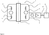
- a prefered advantageous embodiment is, that the current sensor, voltage sensor and electrodes for harvesting system are implemented together in one common, for example toroidal sensor housing in that way, that the current sensor coil is arranged in the middle between the voltage electrodes and electrodes for harvesting, see detailed description below.
- impedance matching element is not limited to existing sensing devices already installed in the applications but can be easily connected with new produced devices, with at least one magnetic field sensor and/or at least one electric field sensor.
- Combined sensing device 1 consists of insulating material 2, that provides sufficient dielectric strength, depending on the voltage level applied on primary conductor 3.
- Current sensing part 4 senses magnetic field that is proportional to the current flowing through the primary conductor 3.
- Voltage sensing part consists of primary capacitance created between primary conductor 3 and capacitive electrode 5 and secondary capacitance created between capacitive electrode 5 and shielding electrode 6. Shielding electrode 6 protect capacitive electrode 5 from external electric fields, thus shielding from external disturbances. In case division ratio of capacitances created between primary conductor 3, capacitive electrode 5 and shielding electrode 6 is not sufficient to create required ratio, external capacitors could be electrically connected in parallel to the output of such voltage divider to tune the divider ratio to required level.
- Part for harvesting consist of primary capacitance created between primary conductor 3 and capacitive electrode 7 and secondary capacitance created between capacitive electrode 8. The required ratio is achieved by using external capacitor similarly as described above.
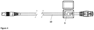
- the harvesting system 9 is a part of the cable connection 10 that connects the sensing device with a measuring device.
- an analog or a digital output can be provided.
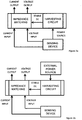
- the harvesting system 9 is placed in cable connection 10 according to Fig. 3 , if non-conventional power source are used (internal supply, see Fig. 2a ).
- the harvesting system can be powered directly from measured device.
- the harvesting system 9 is placed in cable connection 10 according to Fig. 4 (external poer source, see Fig. 2b ).
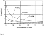
- the proposed sensing device has strong dependence on input impedance variation of measuring devices. Both amplitude and phase of signal are affected. However, the signal phase affecting is critical in the analyzed frequency range from 10Hz to 100 Hz.
- the proposed sensing device can be used together with all types measuring devices without any additional reconfiguration during impedance mismatch. Thus, the stability of signal phase and amplitude are independent on input impedance of measuring devices and undesirable phenomenas as shown in Fig. 6 are minimized.
- the harvesting system is optimized for wide bandwidth low power applications, has an extremely high gain-bandwidth to power ratio and is unity gain stable. Thus, the system frequency response does not affect output signal from sensing device. Due to the cable connection additional parasitic load capacitances at the output of sensing device may occur. Its size dependens on many factors as type of cable, cable length etc. It cause further signal degradation.
- the proposed impedance matching element is designed to directly drive up to 100nF capacitive load in unity gain. Higher gain configurations tend to have better capacitive drive capability than lower gain configurations.
- Fig.7 shows the signal integrity improvement if proposed sensing device is used. Especially at the low frequencies (below 100Hz) the error reduction is significant.
Landscapes
- Physics & Mathematics (AREA)
- General Physics & Mathematics (AREA)
- Measuring Instrument Details And Bridges, And Automatic Balancing Devices (AREA)
Claims (10)
- Dispositif de détection de courant et/ou de tension pour une utilisation par intégration dans des systèmes électriques, avec au moins un capteur de champ magnétique et/ou au moins un capteur de champ électrique, dans lequel
le capteur de champ électrique et/ou le capteur de champ magnétique sont branchés à un élément d'adaptation d'impédance, qui permet un branchement à un dispositif de mesure analogique indépendant et est alimenté à partir d'un dispositif de collecte d'énergie, fournissant une alimentation électrique stable à l'élément d'adaptation d'impédance, qui fait partie intégrante d'une carte électronique d'adaptation d'impédance, et dans lequel le dispositif de collecte d'énergie (9) fait partie d'un branchement par câble (10), qui branche le dispositif de détection au dispositif de mesure. - Dispositif de détection de courant et/ou de tension selon la revendication 1,
dans lequel le dispositif de collecte d'énergie est alimenté à partir du capteur de champ magnétique et/ou de champ électrique. - Dispositif de détection de courant et/ou de tension selon la revendication 1,
dans lequel le dispositif de collecte d'énergie est configuré pour être alimenté à partir d'une source d'alimentation externe. - Dispositif de détection de courant et/ou de tension selon l'une quelconque des revendications susmentionnées,
dans lequel l'élément d'adaptation d'impédance est configuré pour fournir une sortie proportionnelle aux quantités mesurées, telles qu'un champ électrique et/ou magnétique, et est indépendant de l'impédance d'entrée du dispositif branché. - Dispositif de détection de courant et/ou de tension selon l'une quelconque des revendications susmentionnées,
dans lequel l'élément d'adaptation d'impédance peut en outre conditionner des signaux de sortie. - Dispositif de détection de courant et/ou de tension selon l'une quelconque des revendications susmentionnées,
dans lequel l'élément d'adaptation d'impédance peut fournir une sortie numérique. - Dispositif de détection de courant et/ou de tension selon l'une quelconque des revendications susmentionnées,
dans lequel l'élément d'adaptation d'impédance est branché à un câble de sortie dudit dispositif. - Dispositif de détection de courant et/ou de tension selon l'une quelconque des revendications susmentionnées,
dans lequel l'élément d'adaptation d'impédance peut être branché non seulement à de nouveaux dispositifs produits, mais aussi à des dispositifs de détection existants déjà installés dans les applications, convenant ainsi à des fins de mise à niveau. - Dispositif de détection de courant et/ou de tension selon l'une quelconque des revendications susmentionnées,
dans lequel l'élément d'adaptation d'impédance a une surveillance interne et/ou des diagnostics de ses fonctions. - Dispositif de détection de courant et/ou de tension selon la revendication 2,
dans lequel le dispositif de collecte d'énergie est alimenté à partir d'un capteur de champ électrique mis en œuvre sous la forme d'un diviseur de tension capacitif.
Priority Applications (3)
| Application Number | Priority Date | Filing Date | Title |
|---|---|---|---|
| EP14001713.8A EP2944967B1 (fr) | 2014-05-15 | 2014-05-15 | Élément d'adaptation d'impédance pour la tension et/ou les dispositifs de détection de courant |
| CN201510364088.XA CN105092926A (zh) | 2014-05-15 | 2015-05-15 | 用于电压和/或电流感测器件的阻抗匹配元件 |
| US14/713,625 US9859865B2 (en) | 2014-05-15 | 2015-05-15 | Impedance matching element for voltage and/or current sensing devices |
Applications Claiming Priority (1)
| Application Number | Priority Date | Filing Date | Title |
|---|---|---|---|
| EP14001713.8A EP2944967B1 (fr) | 2014-05-15 | 2014-05-15 | Élément d'adaptation d'impédance pour la tension et/ou les dispositifs de détection de courant |
Publications (2)
| Publication Number | Publication Date |
|---|---|
| EP2944967A1 EP2944967A1 (fr) | 2015-11-18 |
| EP2944967B1 true EP2944967B1 (fr) | 2020-08-05 |
Family
ID=50732740
Family Applications (1)
| Application Number | Title | Priority Date | Filing Date |
|---|---|---|---|
| EP14001713.8A Not-in-force EP2944967B1 (fr) | 2014-05-15 | 2014-05-15 | Élément d'adaptation d'impédance pour la tension et/ou les dispositifs de détection de courant |
Country Status (3)
| Country | Link |
|---|---|
| US (1) | US9859865B2 (fr) |
| EP (1) | EP2944967B1 (fr) |
| CN (1) | CN105092926A (fr) |
Families Citing this family (6)
| Publication number | Priority date | Publication date | Assignee | Title |
|---|---|---|---|---|
| JP6895122B2 (ja) * | 2017-09-14 | 2021-06-30 | 三菱電機株式会社 | カレントモニタ及びカレントモニタ用中継装置 |
| EP3578998B1 (fr) | 2018-06-08 | 2024-09-04 | 3M Innovative Properties Company | Ensemble d'impédance |
| CN112236681B (zh) * | 2018-06-08 | 2024-06-18 | 3M创新有限公司 | 阻抗组件 |
| FR3090925B1 (fr) * | 2018-12-19 | 2021-03-19 | Continental Automotive France | Dispositif de détection automatique de couplage entre dispositifs électronique |
| DE112020001835T5 (de) * | 2019-04-10 | 2022-01-13 | Iee International Electronics & Engineering S.A. | Mehrkanal-Kapazitäts-Abtastmessschaltung |
| CN110531161B (zh) * | 2019-07-29 | 2020-10-23 | 北京航空航天大学 | 一种印刷电路板各位置输入阻抗非接触式在线测试装置 |
Family Cites Families (11)
| Publication number | Priority date | Publication date | Assignee | Title |
|---|---|---|---|---|
| FR2698696B1 (fr) * | 1992-11-27 | 1995-01-06 | Simplex Appareils | Ensemble de mesure de tension pour réseau de distribution électrique. |
| GB0605717D0 (en) * | 2006-03-21 | 2006-05-03 | Univ Sussex | Electric potential sensor |
| FR2940457B1 (fr) * | 2008-12-18 | 2011-02-18 | Schneider Electric Ind Sas | Dispositif diviseur capacitif, capteur de tension, module de declencheur et appareil de protection electrique pourvus d'un tel dispositif |
| CN103105515A (zh) * | 2011-11-14 | 2013-05-15 | 北京北方微电子基地设备工艺研究中心有限责任公司 | 一种电流传感器、阻抗匹配器以及等离子体加工设备 |
| JP5864313B2 (ja) * | 2012-03-14 | 2016-02-17 | 株式会社ダイヘン | 校正パラメータ生成システム |
| EP2653846A1 (fr) * | 2012-04-18 | 2013-10-23 | Nxp B.V. | Circuit de capteur et procédé d'étalonnage |
| CN104584144B (zh) * | 2012-08-17 | 2017-10-24 | 马里亚诺·洛佩斯戈麦斯 | 包括电力电缆和能量采集设备的用于照亮电缆等用途的能量采集系统,该系统的制造与维修方法 |
| WO2014042681A2 (fr) * | 2012-09-11 | 2014-03-20 | Access Business Group International Llc | Commande de puissance sans fil |
| EP2722678A1 (fr) * | 2012-10-18 | 2014-04-23 | ABB Technology AG | Dispositif de détection de courant et/ou de tension pour utilisation intégrante |
| CN102981058B (zh) * | 2012-12-05 | 2015-03-11 | 辽宁省电力有限公司抚顺供电公司 | 抗干扰直流电阻测试装置 |
| CN203376391U (zh) * | 2013-07-29 | 2014-01-01 | 北京无线电计量测试研究所 | 一种采用阻抗匹配连接器的脉冲电流测量装置 |
-
2014
- 2014-05-15 EP EP14001713.8A patent/EP2944967B1/fr not_active Not-in-force
-
2015
- 2015-05-15 US US14/713,625 patent/US9859865B2/en not_active Expired - Fee Related
- 2015-05-15 CN CN201510364088.XA patent/CN105092926A/zh active Pending
Non-Patent Citations (1)
| Title |
|---|
| None * |
Also Published As
| Publication number | Publication date |
|---|---|
| US9859865B2 (en) | 2018-01-02 |
| EP2944967A1 (fr) | 2015-11-18 |
| US20150333725A1 (en) | 2015-11-19 |
| CN105092926A (zh) | 2015-11-25 |
Similar Documents
| Publication | Publication Date | Title |
|---|---|---|
| US9859865B2 (en) | Impedance matching element for voltage and/or current sensing devices | |
| US8125291B2 (en) | Electromagnetic interference noise separator | |
| US6614218B1 (en) | Current measuring device | |
| US12092663B2 (en) | Sensor part for installation in medium-voltage cable compartments and a device for measuring a voltage in medium-voltage circuits comprising such sensor part | |
| US6717395B2 (en) | Current transformer based high voltage measurement apparatus | |
| US10320279B2 (en) | Power supplies and methods for reducing common mode noise | |
| US10436821B2 (en) | Apparatus for detecting AC components in a DC circuit and use of the apparatus | |
| US10168361B2 (en) | Current sensor and measuring apparatus | |
| US8278947B2 (en) | Capacitive divider device, voltage sensor, trip device module and electrical protection apparatus provided with such a device | |
| US12130308B2 (en) | Adjustable voltage sensor | |
| US6529013B2 (en) | Three-phase voltage sensor with active crosstalk cancellation | |
| US11469013B2 (en) | Combination of an electricity conducting element, such as bushing, and a connector cable | |
| JP2007514148A5 (fr) | ||
| CN103339860A (zh) | 电容性近接传感器以及用于电容性近接检测的方法 | |
| US20180372779A1 (en) | Measurement input circuit and measurement device | |
| CN112997086A (zh) | 电压传感器和装置 | |
| US10345342B2 (en) | Rogowski current with active capacitance compensation | |
| US10782320B2 (en) | Method and sensor for measuring an alternating current | |
| EP1923709B1 (fr) | Capteur de courant linéaire actif | |
| US20250182926A1 (en) | Connection conductor, arrangement having a connection conductor and use of a connection conductor | |
| US20250035679A1 (en) | Active probe for measuring voltage at high impedances | |
| CN120685948A (zh) | 用于测量导体的电流值并校正所测量的电流值的测量系统 | |
| US10288647B2 (en) | Coaxial design for secondary unit | |
| JP2013217759A (ja) | 電圧検出装置 | |
| PL220192B1 (pl) | Izolowany układ do pomiaru harmonicznych sygnałów elektroenergetycznych wysokiego napięcia |
Legal Events
| Date | Code | Title | Description |
|---|---|---|---|
| PUAI | Public reference made under article 153(3) epc to a published international application that has entered the european phase |
Free format text: ORIGINAL CODE: 0009012 |
|
| AK | Designated contracting states |
Kind code of ref document: A1 Designated state(s): AL AT BE BG CH CY CZ DE DK EE ES FI FR GB GR HR HU IE IS IT LI LT LU LV MC MK MT NL NO PL PT RO RS SE SI SK SM TR |
|
| AX | Request for extension of the european patent |
Extension state: BA ME |
|
| 17P | Request for examination filed |
Effective date: 20160513 |
|
| RBV | Designated contracting states (corrected) |
Designated state(s): AL AT BE BG CH CY CZ DE DK EE ES FI FR GB GR HR HU IE IS IT LI LT LU LV MC MK MT NL NO PL PT RO RS SE SI SK SM TR |
|
| RAP1 | Party data changed (applicant data changed or rights of an application transferred) |
Owner name: ABB SCHWEIZ AG |
|
| GRAP | Despatch of communication of intention to grant a patent |
Free format text: ORIGINAL CODE: EPIDOSNIGR1 |
|
| STAA | Information on the status of an ep patent application or granted ep patent |
Free format text: STATUS: GRANT OF PATENT IS INTENDED |
|
| INTG | Intention to grant announced |
Effective date: 20190708 |
|
| GRAJ | Information related to disapproval of communication of intention to grant by the applicant or resumption of examination proceedings by the epo deleted |
Free format text: ORIGINAL CODE: EPIDOSDIGR1 |
|
| STAA | Information on the status of an ep patent application or granted ep patent |
Free format text: STATUS: REQUEST FOR EXAMINATION WAS MADE |
|
| GRAP | Despatch of communication of intention to grant a patent |
Free format text: ORIGINAL CODE: EPIDOSNIGR1 |
|
| STAA | Information on the status of an ep patent application or granted ep patent |
Free format text: STATUS: GRANT OF PATENT IS INTENDED |
|
| INTC | Intention to grant announced (deleted) | ||
| INTG | Intention to grant announced |
Effective date: 20200311 |
|
| RIN1 | Information on inventor provided before grant (corrected) |
Inventor name: SEVCIK, BRETISLAV Inventor name: VELESIK, PETR Inventor name: JAVORA, RADEK |
|
| GRAS | Grant fee paid |
Free format text: ORIGINAL CODE: EPIDOSNIGR3 |
|
| GRAA | (expected) grant |
Free format text: ORIGINAL CODE: 0009210 |
|
| STAA | Information on the status of an ep patent application or granted ep patent |
Free format text: STATUS: THE PATENT HAS BEEN GRANTED |
|
| AK | Designated contracting states |
Kind code of ref document: B1 Designated state(s): AL AT BE BG CH CY CZ DE DK EE ES FI FR GB GR HR HU IE IS IT LI LT LU LV MC MK MT NL NO PL PT RO RS SE SI SK SM TR |
|
| REG | Reference to a national code |
Ref country code: GB Ref legal event code: FG4D |
|
| REG | Reference to a national code |
Ref country code: CH Ref legal event code: EP |
|
| REG | Reference to a national code |
Ref country code: AT Ref legal event code: REF Ref document number: 1299452 Country of ref document: AT Kind code of ref document: T Effective date: 20200815 |
|
| REG | Reference to a national code |
Ref country code: DE Ref legal event code: R096 Ref document number: 602014068472 Country of ref document: DE |
|
| REG | Reference to a national code |
Ref country code: IE Ref legal event code: FG4D |
|
| REG | Reference to a national code |
Ref country code: LT Ref legal event code: MG4D |
|
| REG | Reference to a national code |
Ref country code: NL Ref legal event code: MP Effective date: 20200805 |
|
| PG25 | Lapsed in a contracting state [announced via postgrant information from national office to epo] |
Ref country code: BG Free format text: LAPSE BECAUSE OF FAILURE TO SUBMIT A TRANSLATION OF THE DESCRIPTION OR TO PAY THE FEE WITHIN THE PRESCRIBED TIME-LIMIT Effective date: 20201105 Ref country code: LT Free format text: LAPSE BECAUSE OF FAILURE TO SUBMIT A TRANSLATION OF THE DESCRIPTION OR TO PAY THE FEE WITHIN THE PRESCRIBED TIME-LIMIT Effective date: 20200805 Ref country code: FI Free format text: LAPSE BECAUSE OF FAILURE TO SUBMIT A TRANSLATION OF THE DESCRIPTION OR TO PAY THE FEE WITHIN THE PRESCRIBED TIME-LIMIT Effective date: 20200805 Ref country code: SE Free format text: LAPSE BECAUSE OF FAILURE TO SUBMIT A TRANSLATION OF THE DESCRIPTION OR TO PAY THE FEE WITHIN THE PRESCRIBED TIME-LIMIT Effective date: 20200805 Ref country code: HR Free format text: LAPSE BECAUSE OF FAILURE TO SUBMIT A TRANSLATION OF THE DESCRIPTION OR TO PAY THE FEE WITHIN THE PRESCRIBED TIME-LIMIT Effective date: 20200805 Ref country code: NO Free format text: LAPSE BECAUSE OF FAILURE TO SUBMIT A TRANSLATION OF THE DESCRIPTION OR TO PAY THE FEE WITHIN THE PRESCRIBED TIME-LIMIT Effective date: 20201105 Ref country code: PT Free format text: LAPSE BECAUSE OF FAILURE TO SUBMIT A TRANSLATION OF THE DESCRIPTION OR TO PAY THE FEE WITHIN THE PRESCRIBED TIME-LIMIT Effective date: 20201207 Ref country code: ES Free format text: LAPSE BECAUSE OF FAILURE TO SUBMIT A TRANSLATION OF THE DESCRIPTION OR TO PAY THE FEE WITHIN THE PRESCRIBED TIME-LIMIT Effective date: 20200805 Ref country code: GR Free format text: LAPSE BECAUSE OF FAILURE TO SUBMIT A TRANSLATION OF THE DESCRIPTION OR TO PAY THE FEE WITHIN THE PRESCRIBED TIME-LIMIT Effective date: 20201106 |
|
| PG25 | Lapsed in a contracting state [announced via postgrant information from national office to epo] |
Ref country code: IS Free format text: LAPSE BECAUSE OF FAILURE TO SUBMIT A TRANSLATION OF THE DESCRIPTION OR TO PAY THE FEE WITHIN THE PRESCRIBED TIME-LIMIT Effective date: 20201205 Ref country code: LV Free format text: LAPSE BECAUSE OF FAILURE TO SUBMIT A TRANSLATION OF THE DESCRIPTION OR TO PAY THE FEE WITHIN THE PRESCRIBED TIME-LIMIT Effective date: 20200805 Ref country code: RS Free format text: LAPSE BECAUSE OF FAILURE TO SUBMIT A TRANSLATION OF THE DESCRIPTION OR TO PAY THE FEE WITHIN THE PRESCRIBED TIME-LIMIT Effective date: 20200805 Ref country code: PL Free format text: LAPSE BECAUSE OF FAILURE TO SUBMIT A TRANSLATION OF THE DESCRIPTION OR TO PAY THE FEE WITHIN THE PRESCRIBED TIME-LIMIT Effective date: 20200805 Ref country code: NL Free format text: LAPSE BECAUSE OF FAILURE TO SUBMIT A TRANSLATION OF THE DESCRIPTION OR TO PAY THE FEE WITHIN THE PRESCRIBED TIME-LIMIT Effective date: 20200805 |
|
| PG25 | Lapsed in a contracting state [announced via postgrant information from national office to epo] |
Ref country code: SM Free format text: LAPSE BECAUSE OF FAILURE TO SUBMIT A TRANSLATION OF THE DESCRIPTION OR TO PAY THE FEE WITHIN THE PRESCRIBED TIME-LIMIT Effective date: 20200805 Ref country code: RO Free format text: LAPSE BECAUSE OF FAILURE TO SUBMIT A TRANSLATION OF THE DESCRIPTION OR TO PAY THE FEE WITHIN THE PRESCRIBED TIME-LIMIT Effective date: 20200805 Ref country code: EE Free format text: LAPSE BECAUSE OF FAILURE TO SUBMIT A TRANSLATION OF THE DESCRIPTION OR TO PAY THE FEE WITHIN THE PRESCRIBED TIME-LIMIT Effective date: 20200805 Ref country code: DK Free format text: LAPSE BECAUSE OF FAILURE TO SUBMIT A TRANSLATION OF THE DESCRIPTION OR TO PAY THE FEE WITHIN THE PRESCRIBED TIME-LIMIT Effective date: 20200805 Ref country code: CZ Free format text: LAPSE BECAUSE OF FAILURE TO SUBMIT A TRANSLATION OF THE DESCRIPTION OR TO PAY THE FEE WITHIN THE PRESCRIBED TIME-LIMIT Effective date: 20200805 |
|
| REG | Reference to a national code |
Ref country code: DE Ref legal event code: R097 Ref document number: 602014068472 Country of ref document: DE |
|
| REG | Reference to a national code |
Ref country code: AT Ref legal event code: UEP Ref document number: 1299452 Country of ref document: AT Kind code of ref document: T Effective date: 20200805 |
|
| PG25 | Lapsed in a contracting state [announced via postgrant information from national office to epo] |
Ref country code: AL Free format text: LAPSE BECAUSE OF FAILURE TO SUBMIT A TRANSLATION OF THE DESCRIPTION OR TO PAY THE FEE WITHIN THE PRESCRIBED TIME-LIMIT Effective date: 20200805 |
|
| PLBE | No opposition filed within time limit |
Free format text: ORIGINAL CODE: 0009261 |
|
| STAA | Information on the status of an ep patent application or granted ep patent |
Free format text: STATUS: NO OPPOSITION FILED WITHIN TIME LIMIT |
|
| PG25 | Lapsed in a contracting state [announced via postgrant information from national office to epo] |
Ref country code: SK Free format text: LAPSE BECAUSE OF FAILURE TO SUBMIT A TRANSLATION OF THE DESCRIPTION OR TO PAY THE FEE WITHIN THE PRESCRIBED TIME-LIMIT Effective date: 20200805 |
|
| 26N | No opposition filed |
Effective date: 20210507 |
|
| PG25 | Lapsed in a contracting state [announced via postgrant information from national office to epo] |
Ref country code: IT Free format text: LAPSE BECAUSE OF FAILURE TO SUBMIT A TRANSLATION OF THE DESCRIPTION OR TO PAY THE FEE WITHIN THE PRESCRIBED TIME-LIMIT Effective date: 20200805 |
|
| PG25 | Lapsed in a contracting state [announced via postgrant information from national office to epo] |
Ref country code: SI Free format text: LAPSE BECAUSE OF FAILURE TO SUBMIT A TRANSLATION OF THE DESCRIPTION OR TO PAY THE FEE WITHIN THE PRESCRIBED TIME-LIMIT Effective date: 20200805 |
|
| REG | Reference to a national code |
Ref country code: CH Ref legal event code: PL |
|
| GBPC | Gb: european patent ceased through non-payment of renewal fee |
Effective date: 20210515 |
|
| PG25 | Lapsed in a contracting state [announced via postgrant information from national office to epo] |
Ref country code: CH Free format text: LAPSE BECAUSE OF NON-PAYMENT OF DUE FEES Effective date: 20210531 Ref country code: LU Free format text: LAPSE BECAUSE OF NON-PAYMENT OF DUE FEES Effective date: 20210515 Ref country code: LI Free format text: LAPSE BECAUSE OF NON-PAYMENT OF DUE FEES Effective date: 20210531 Ref country code: MC Free format text: LAPSE BECAUSE OF FAILURE TO SUBMIT A TRANSLATION OF THE DESCRIPTION OR TO PAY THE FEE WITHIN THE PRESCRIBED TIME-LIMIT Effective date: 20200805 |
|
| REG | Reference to a national code |
Ref country code: BE Ref legal event code: MM Effective date: 20210531 |
|
| PG25 | Lapsed in a contracting state [announced via postgrant information from national office to epo] |
Ref country code: IE Free format text: LAPSE BECAUSE OF NON-PAYMENT OF DUE FEES Effective date: 20210515 Ref country code: GB Free format text: LAPSE BECAUSE OF NON-PAYMENT OF DUE FEES Effective date: 20210515 |
|
| PG25 | Lapsed in a contracting state [announced via postgrant information from national office to epo] |
Ref country code: FR Free format text: LAPSE BECAUSE OF NON-PAYMENT OF DUE FEES Effective date: 20210531 |
|
| PG25 | Lapsed in a contracting state [announced via postgrant information from national office to epo] |
Ref country code: BE Free format text: LAPSE BECAUSE OF NON-PAYMENT OF DUE FEES Effective date: 20210531 |
|
| PG25 | Lapsed in a contracting state [announced via postgrant information from national office to epo] |
Ref country code: HU Free format text: LAPSE BECAUSE OF FAILURE TO SUBMIT A TRANSLATION OF THE DESCRIPTION OR TO PAY THE FEE WITHIN THE PRESCRIBED TIME-LIMIT; INVALID AB INITIO Effective date: 20140515 |
|
| PG25 | Lapsed in a contracting state [announced via postgrant information from national office to epo] |
Ref country code: CY Free format text: LAPSE BECAUSE OF FAILURE TO SUBMIT A TRANSLATION OF THE DESCRIPTION OR TO PAY THE FEE WITHIN THE PRESCRIBED TIME-LIMIT Effective date: 20200805 |
|
| PG25 | Lapsed in a contracting state [announced via postgrant information from national office to epo] |
Ref country code: MK Free format text: LAPSE BECAUSE OF FAILURE TO SUBMIT A TRANSLATION OF THE DESCRIPTION OR TO PAY THE FEE WITHIN THE PRESCRIBED TIME-LIMIT Effective date: 20200805 |
|
| PGFP | Annual fee paid to national office [announced via postgrant information from national office to epo] |
Ref country code: DE Payment date: 20240521 Year of fee payment: 11 |
|
| PGFP | Annual fee paid to national office [announced via postgrant information from national office to epo] |
Ref country code: AT Payment date: 20240522 Year of fee payment: 11 |
|
| PG25 | Lapsed in a contracting state [announced via postgrant information from national office to epo] |
Ref country code: MT Free format text: LAPSE BECAUSE OF FAILURE TO SUBMIT A TRANSLATION OF THE DESCRIPTION OR TO PAY THE FEE WITHIN THE PRESCRIBED TIME-LIMIT Effective date: 20200805 |
|
| REG | Reference to a national code |
Ref country code: DE Ref legal event code: R119 Ref document number: 602014068472 Country of ref document: DE |
|
| PG25 | Lapsed in a contracting state [announced via postgrant information from national office to epo] |
Ref country code: TR Free format text: LAPSE BECAUSE OF FAILURE TO SUBMIT A TRANSLATION OF THE DESCRIPTION OR TO PAY THE FEE WITHIN THE PRESCRIBED TIME-LIMIT Effective date: 20200805 |
|
| PG25 | Lapsed in a contracting state [announced via postgrant information from national office to epo] |
Ref country code: AT Free format text: LAPSE BECAUSE OF NON-PAYMENT OF DUE FEES Effective date: 20250515 |
|
| REG | Reference to a national code |
Ref country code: AT Ref legal event code: MM01 Ref document number: 1299452 Country of ref document: AT Kind code of ref document: T Effective date: 20250515 |
|
| PG25 | Lapsed in a contracting state [announced via postgrant information from national office to epo] |
Ref country code: DE Free format text: LAPSE BECAUSE OF NON-PAYMENT OF DUE FEES Effective date: 20251202 |