EP2944975A1 - Dispositif de mesure d'une taille physique se modifiant, par exemple la pression - Google Patents
Dispositif de mesure d'une taille physique se modifiant, par exemple la pression Download PDFInfo
- Publication number
- EP2944975A1 EP2944975A1 EP15167527.9A EP15167527A EP2944975A1 EP 2944975 A1 EP2944975 A1 EP 2944975A1 EP 15167527 A EP15167527 A EP 15167527A EP 2944975 A1 EP2944975 A1 EP 2944975A1
- Authority
- EP
- European Patent Office
- Prior art keywords
- signal
- analog
- frequency
- digital
- amplifier
- Prior art date
- Legal status (The legal status is an assumption and is not a legal conclusion. Google has not performed a legal analysis and makes no representation as to the accuracy of the status listed.)
- Granted
Links
Images
Classifications
-
- H—ELECTRICITY
- H03—ELECTRONIC CIRCUITRY
- H03M—CODING; DECODING; CODE CONVERSION IN GENERAL
- H03M3/00—Conversion of analogue values to or from differential modulation
- H03M3/30—Delta-sigma modulation
- H03M3/322—Continuously compensating for, or preventing, undesired influence of physical parameters
- H03M3/324—Continuously compensating for, or preventing, undesired influence of physical parameters characterised by means or methods for compensating or preventing more than one type of error at a time, e.g. by synchronisation or using a ratiometric arrangement
- H03M3/326—Continuously compensating for, or preventing, undesired influence of physical parameters characterised by means or methods for compensating or preventing more than one type of error at a time, e.g. by synchronisation or using a ratiometric arrangement by averaging out the errors
- H03M3/338—Continuously compensating for, or preventing, undesired influence of physical parameters characterised by means or methods for compensating or preventing more than one type of error at a time, e.g. by synchronisation or using a ratiometric arrangement by averaging out the errors by permutation in the time domain, e.g. dynamic element matching
- H03M3/34—Continuously compensating for, or preventing, undesired influence of physical parameters characterised by means or methods for compensating or preventing more than one type of error at a time, e.g. by synchronisation or using a ratiometric arrangement by averaging out the errors by permutation in the time domain, e.g. dynamic element matching by chopping
-
- H—ELECTRICITY
- H03—ELECTRONIC CIRCUITRY
- H03M—CODING; DECODING; CODE CONVERSION IN GENERAL
- H03M1/00—Analogue/digital conversion; Digital/analogue conversion
- H03M1/06—Continuously compensating for, or preventing, undesired influence of physical parameters
- H03M1/0617—Continuously compensating for, or preventing, undesired influence of physical parameters characterised by the use of methods or means not specific to a particular type of detrimental influence
- H03M1/0634—Continuously compensating for, or preventing, undesired influence of physical parameters characterised by the use of methods or means not specific to a particular type of detrimental influence by averaging out the errors, e.g. using sliding scale
- H03M1/0656—Continuously compensating for, or preventing, undesired influence of physical parameters characterised by the use of methods or means not specific to a particular type of detrimental influence by averaging out the errors, e.g. using sliding scale in the time domain, e.g. using intended jitter as a dither signal
Definitions
- the invention relates to a device for measuring a changing physical quantity, which is, for example, the pressure.
- Measuring devices for detecting physical quantities are known.
- appropriate sensors are used, which output an analog measuring signal, that is to transform the physical variable to be measured into a measuring signal.
- These measuring signals are sometimes very small and possibly also very noisy.
- the measurement signals may be offset-related.
- the measuring signals are processed in a signal processing unit, wherein a measuring amplifier is arranged at the input of such a signal processing unit, which can be offset as well as noisy.
- the object of the invention is to provide a device for measuring a changing physical size, in which with the least possible effort an improved noise reduction can be achieved.
- the invention is based on the knowledge that with so-called chopper concepts basically an improved noise suppression can be achieved.
- the problem with such chopper concepts is that the complexity of the frequency mixers for up and down mixing of the measurement signal to be processed is circuitry-consuming.
- sinusoidal frequency mixers are used as frequency mixers for upmixing the measurement signal, ie for shifting the frequencies of the measurement signal by a shift frequency f D to higher frequencies.
- chopper concepts are used, for example, to more easily suppress amplifier offsets and low-frequency amplifier noise (so-called 1 / f noise).
- the sine frequency mixer is thus an analog circuit, since the signal to be amplified by the amplifier is an analog signal (measurement signal of the sensor).
- the realization of an analog-sine frequency mixer is quite complex, which is why an analog-rectangular frequency mixer is used according to the invention.
- the downmixing is subsequently realized by a sine-frequency mixer which can be implemented digitally and thus can be realized much simpler than a sine-frequency mixer for analog signals.
- the hardware effort to be operated for noise suppression improvement (namely for downmixing the processed measurement signal) is "shifted" to the digital domain of the inventive device by having the analog-to-digital converter in the "chopped" part of the signal path and so that the digital signal is shuffled down.
- the invention makes use of the fact that a sine-frequency mixer for downmixing, ie for shifting the frequencies about the shift frequency f D to lower frequencies, can be realized quite simply as a digital frequency mixer, whereas as a frequency mixer for up-mixing the frequencies of the analog measurement signal by Shift frequency f D to higher frequencies out as analog-square frequency mixer is executed.
- the rectangular mixer is at Upmixing is far more appropriate than a sine mixer, as the fundamental wave of the rectangle 4 / ⁇ is larger than the sine mixer. You can thereby achieve a signal (energy) gain of about 27%.
- the highly mixed signal also contains mixed products at the odd multiples of the fundamental frequency of the rectangle. However, they are advantageously not downmixed if, as suggested by the invention, a sine mixer is used for downmixing. When mixing back with a rectangular mixer, the high-frequency converter noise is also mixed back.
- an essential aspect of the invention is the combination of using a rectangular mixer to up-mix the analog signal, amplify the high-mix signal, analog-to-digital conversion of the high-mix signal, and down-mix the digital signal using a sine mixer.
- a further downstream of the digital sine frequency mixer arranged at the output of the signal processing unit first filter for suppressing caused by the analog-square frequency mixer and by the digital sine frequency mixer in the frequency shifted down signal points at odd harmonics of the shift frequency f D be provided.
- a further expedient embodiment of the invention can be characterized by a further, the digital sine frequency mixer downstream, arranged at the output of the signal processing unit band-pass filter for band limiting the output signal of the digital sine frequency mixer or the first filter.
- analog-to-digital converter is designed as a monotonously operating or substantially monotone analog-to-digital converter.
- the analog-to-digital converter is designed as a delta-sigma converter that the delta-sigma converter to a decimation filter for filtering noise in the digital signal to form a phase shift of the filtered digital signal an output of the decimation filter is connected downstream and that is connected between the delta-sigma converter and the decimation filter, a digital phase shifter for compensating the phase rotation resulting from the decimation.
- analog-to-digital converter is designed as a SAR (Successive Approximation Register) converter.
- the senor has a measuring bridge circuit.
- This sensor or measuring bridge circuit can be designed as a voltage generator, in particular a differential voltage converter, as a Wheatstone bridge, which primarily comprises a piezoresistive component as e.g. Pressure sensor has.
- the sensor generates a differential voltage from a physical measured variable, as may be the case, for example, with a thermocouple.
- Other sensor concepts are also conceivable.
- the senor outputs a measurement signal bearing a sensor offset and that the sensor offset can be shifted by means of a further analog-rectangular frequency mixer by the shift frequency f D to higher frequencies and the signal path between the sensor and the ADC before, behind or in the amplifier to form a difference with the relevant signal before, behind or in the amplifier can be fed.
- the amplifier has a first amplifier stage for Pre-amplification of the analog measurement signal and a second amplifier stage, wherein the present after the second amplifier stage amplified analog signal can be supplied to the analog-to-digital converter, and in that shifted by the shift frequency f D sensor offset of the second amplifier stage to form a difference with the output signal the first amplifier stage can be fed.
- Powerful auto zero measurement amplifiers such as are used to amplify analog measurement signals from, for example, pressure sensors or sensors for other physical parameters, have noise power densities in ranges that are inadequate for a variety of applications. For a sensor system to be virtually “transparent”, noise values are required which are significantly smaller than the noise power densities of currently available measuring amplifiers. Investigations have shown that chopper concepts can basically cause a better noise suppression. In the inventive concept, the hardware overhead for noise suppression is shifted into the digital domain of an apparatus for measuring a changing physical quantity, such as pressure, by switching the analog-to-digital converter into the chopped signal path.
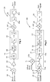
- Fig. 1 shows a first embodiment of such a circuit concept.
- the signal of a measuring bridge or a sensor 10 is using a Analog-rectangular frequency mixer 12 (also called Umtaster) by a shift frequency f D shifted to higher frequencies.
- the measuring signal of the sensor 10 is an alternating signal, which is amplified in a downstream (measuring) amplifier 14.
- the advantage here is that due to the chopper concept in this amplifier 14 no further measures to suppress its offset must be made.
- the amplifier 14 can be kept relatively simple circuitry. Only its bandwidth must be sufficiently large to amplify the frequency-mixed measurement signals without errors.
- the signal mixed up in frequency has mixed products not only at the fundamental frequency (shift frequency f D ) but also at the frequencies of the odd harmonics of the fundamental frequency caused by the analog square wave mixer 12 (even harmonic waves do not exist), however, according to the inventive concept later be suppressed or filtered out with minimal effort.
- the amplifier 14 is followed by an analog-to-digital converter 16, which is formed in this embodiment as a delta-sigma converter 18 with a downstream digital phase shifter 20 and a decimation filter 22.
- the decimation filter 22 filters the noise of the delta-sigma converter 18 and converts the 1-bit signal of the converter into a signal having a width of several bits.
- the phase rotation of the signal resulting from this filtering is brought to a value by the digital phase shifter 20 connected upstream of the decimation filter 22, so that the chopped signal is in phase with a second mixer.
- This second mixer is designed as a digital sine-frequency mixer 24.
- This digital sine frequency mixer 24 shifts the signal by the shift frequency f D to lower frequencies without mixing down the mixed products caused by the analog rectangular mixer during upmixing with the odd harmonics of the rectangular fundamental frequency.
- the design of the mixer as a rectangular mixer would have the disadvantage that noise components would also be down-mixed at odd-numbered multiples of the mixer frequency.
- Another filter 26 with the components 26a and 26b at the output of the signal processing unit 28 of analog-to-digital converter 16, analog-square frequency mixer 12 and digital sine frequency mixer 24 is the band limitation (filter component 26b) and the suppression (filter component 26a) of the down-mixed mixed products the odd harmonics of the fundamental frequency, which are due to the analog-rectangular frequency mixer 12.
- Fig. 2 shows an alternative circuit concept, in which the possibility is given within the signal amplification path an offset, for example, caused by the offset voltage of the measuring bridge or the sensor 10 deducted. Thus, the gain can be increased significantly. This concept can also be applied if the offset is likewise mixed up by the shift frequency f D in accordance with the input signal.
- amplifier 14 is shown as a two-stage amplifier with first and second amplifier stages 14a, 14b.
- the offset signal of the measuring bridge or the sensor 10 which is highly mixed via an analog-rectangular frequency mixer 12a, can be fed into the signal path before, between or behind the two amplifier stages 14a, 14b.
- the signal processing unit according to the circuit concept Fig. 2 the same components as discussed above in connection with the circuit concept Fig. 1 described and in Fig. 1 is shown why in so far in Fig. 2 the same reference numerals have been used as in FIG Fig. 1 ,
Landscapes
- Engineering & Computer Science (AREA)
- Theoretical Computer Science (AREA)
- Measuring Fluid Pressure (AREA)
Priority Applications (1)
| Application Number | Priority Date | Filing Date | Title |
|---|---|---|---|
| EP15167527.9A EP2944975B1 (fr) | 2014-05-14 | 2015-05-13 | Dispositif de mesure d'une taille physique se modifiant, par exemple la pression |
Applications Claiming Priority (2)
| Application Number | Priority Date | Filing Date | Title |
|---|---|---|---|
| EP14168339 | 2014-05-14 | ||
| EP15167527.9A EP2944975B1 (fr) | 2014-05-14 | 2015-05-13 | Dispositif de mesure d'une taille physique se modifiant, par exemple la pression |
Publications (2)
| Publication Number | Publication Date |
|---|---|
| EP2944975A1 true EP2944975A1 (fr) | 2015-11-18 |
| EP2944975B1 EP2944975B1 (fr) | 2018-04-04 |
Family
ID=50729375
Family Applications (1)
| Application Number | Title | Priority Date | Filing Date |
|---|---|---|---|
| EP15167527.9A Active EP2944975B1 (fr) | 2014-05-14 | 2015-05-13 | Dispositif de mesure d'une taille physique se modifiant, par exemple la pression |
Country Status (1)
| Country | Link |
|---|---|
| EP (1) | EP2944975B1 (fr) |
Cited By (1)
| Publication number | Priority date | Publication date | Assignee | Title |
|---|---|---|---|---|
| CN115865079A (zh) * | 2022-11-22 | 2023-03-28 | 复旦大学 | 一种主备时钟链路高精度相位差测量装置及方法 |
Citations (7)
| Publication number | Priority date | Publication date | Assignee | Title |
|---|---|---|---|---|
| DE19757296A1 (de) * | 1997-12-22 | 1999-07-01 | Rohde & Schwarz | Verfahren zum Bestimmen und Kompensieren der Übertragungsfunktion eines Meßgerätes, insbesondere eines Spektrum-Analysators |
| US6891430B1 (en) * | 2000-07-05 | 2005-05-10 | Cirrus Logic, Inc. | Techniques for signal measurement using a conditionally stable amplifier |
| US20070216562A1 (en) | 2006-01-27 | 2007-09-20 | Montage Technology Group, Ltd. | Integrated DSP for a DC offset cancellation loop |
| US20090079607A1 (en) | 2007-09-26 | 2009-03-26 | Medtronic, Inc. | Chopper-stabilized analog-to-digital converter |
| US20100289682A1 (en) * | 2009-05-12 | 2010-11-18 | Qualcomm Incorporated | Sigma-delta converters and methods for analog-to-digital conversion |
| DE102009029051A1 (de) * | 2009-09-01 | 2011-03-03 | Robert Bosch Gmbh | Verfahren und Vorrichtung zum Bereitstellen eines Reflexionssignals |
| US20110063146A1 (en) * | 2009-09-15 | 2011-03-17 | Texas Instruments Incorporated | Multistage chopper stabilized delta-sigma adc with reduced offset |
-
2015
- 2015-05-13 EP EP15167527.9A patent/EP2944975B1/fr active Active
Patent Citations (7)
| Publication number | Priority date | Publication date | Assignee | Title |
|---|---|---|---|---|
| DE19757296A1 (de) * | 1997-12-22 | 1999-07-01 | Rohde & Schwarz | Verfahren zum Bestimmen und Kompensieren der Übertragungsfunktion eines Meßgerätes, insbesondere eines Spektrum-Analysators |
| US6891430B1 (en) * | 2000-07-05 | 2005-05-10 | Cirrus Logic, Inc. | Techniques for signal measurement using a conditionally stable amplifier |
| US20070216562A1 (en) | 2006-01-27 | 2007-09-20 | Montage Technology Group, Ltd. | Integrated DSP for a DC offset cancellation loop |
| US20090079607A1 (en) | 2007-09-26 | 2009-03-26 | Medtronic, Inc. | Chopper-stabilized analog-to-digital converter |
| US20100289682A1 (en) * | 2009-05-12 | 2010-11-18 | Qualcomm Incorporated | Sigma-delta converters and methods for analog-to-digital conversion |
| DE102009029051A1 (de) * | 2009-09-01 | 2011-03-03 | Robert Bosch Gmbh | Verfahren und Vorrichtung zum Bereitstellen eines Reflexionssignals |
| US20110063146A1 (en) * | 2009-09-15 | 2011-03-17 | Texas Instruments Incorporated | Multistage chopper stabilized delta-sigma adc with reduced offset |
Cited By (1)
| Publication number | Priority date | Publication date | Assignee | Title |
|---|---|---|---|---|
| CN115865079A (zh) * | 2022-11-22 | 2023-03-28 | 复旦大学 | 一种主备时钟链路高精度相位差测量装置及方法 |
Also Published As
| Publication number | Publication date |
|---|---|
| EP2944975B1 (fr) | 2018-04-04 |
Similar Documents
| Publication | Publication Date | Title |
|---|---|---|
| EP2406886B1 (fr) | Dispositif pour convertir des signaux analogiques à plage dynamique élevée en signaux numériques | |
| DE102008023535B4 (de) | Elektronische Vorrichtung und Verfahren zur Auswertung einer variablen Kapazität | |
| EP2041874A1 (fr) | Procédé de traitement de signaux de capteur présentant un décalage et dispositif capteur conçu pour la réalisation du procédé | |
| EP1130782A2 (fr) | Procédé et circuit de conversion analogique-numérique de signaux | |
| EP2651036A1 (fr) | Détecteur d'approximation inductif | |
| DE102004010362A1 (de) | Sensor, insbesondere Magnetfeldsensor, mit Störsignal-Kompensation und Verfahren zur Störsignal-Kompensation eines Sensors | |
| DE102004022572B4 (de) | Integratorschaltung | |
| DE102014113213A1 (de) | Magnetfeldsensoren und systeme mit sensorschaltungsabschnitten mit unterschiedlichen vorspannungen und frequenzbereichen | |
| WO2014036984A1 (fr) | Récepteur radar et procédé de réception de signaux de réception dans un récepteur radar | |
| EP2944975B1 (fr) | Dispositif de mesure d'une taille physique se modifiant, par exemple la pression | |
| DE102008023277A1 (de) | Wandlervorrichtung | |
| DE102019109892B3 (de) | Sensorschaltung und Verfahren zum Filtern eines Sensorsignals | |
| DE10216344A1 (de) | Meßverstärkervorrichtung | |
| DE102017129461B3 (de) | Delta-Sigma-Modulator für Trägerfrequenzmesssysteme | |
| EP4419926B1 (fr) | Dispositif et procédé de détection d'un courant électrique avec fréquence d'échantillonnage optimisée | |
| EP2756599B1 (fr) | Procédé pour amplifier un signal d'écho adapte pour observation de l'environnement d'un véhicule et dispositif pour mettre en oeuvre la méthode | |
| DE102004064185B4 (de) | Sensor, insbesondere Magnetfeldsensor, mit Störsignal-Kompensation und Verfahren zur Störsignal-Kompensation eines Sensors | |
| DE102004050088B4 (de) | Verfahren und Vorrichtung zum Übertragen von Signalen | |
| DE102004027667B4 (de) | Nachbarkanal-Unterdrückungs-Vorrichtung, Empfangsgerät und Verfahren zum Betrieb eines Empfangsgeräts | |
| DE69424931T2 (de) | Analog/Digital-Wandler für niederfrequente, differentielle Signale geringer Amplitude | |
| DE102012110737B4 (de) | Analog-Digital-Wandler-Anordnung | |
| EP2667509B1 (fr) | Filtre numérique | |
| DE102021127129A1 (de) | Vorrichtung und Verfahren zur Erfassung eines elektrischen Leitungsstromes mit optimierter Abtastrate | |
| EP2583070B1 (fr) | Convertisseur de mesure à deux canaux de transmission | |
| DE102021127122B4 (de) | Vorrichtung und Verfahren zur Erfassung eines elektrischen Leitungsstromes mit optimierter Abtastrate |
Legal Events
| Date | Code | Title | Description |
|---|---|---|---|
| PUAI | Public reference made under article 153(3) epc to a published international application that has entered the european phase |
Free format text: ORIGINAL CODE: 0009012 |
|
| AK | Designated contracting states |
Kind code of ref document: A1 Designated state(s): AL AT BE BG CH CY CZ DE DK EE ES FI FR GB GR HR HU IE IS IT LI LT LU LV MC MK MT NL NO PL PT RO RS SE SI SK SM TR |
|
| AX | Request for extension of the european patent |
Extension state: BA ME |
|
| RAP1 | Party data changed (applicant data changed or rights of an application transferred) |
Owner name: ELMOS SEMICONDUCTOR AKTIENGESELLSCHAFT |
|
| RAP1 | Party data changed (applicant data changed or rights of an application transferred) |
Owner name: ELMOS SEMICONDUCTOR AKTIENGESELLSCHAFT |
|
| 17P | Request for examination filed |
Effective date: 20160513 |
|
| RBV | Designated contracting states (corrected) |
Designated state(s): AL AT BE BG CH CY CZ DE DK EE ES FI FR GB GR HR HU IE IS IT LI LT LU LV MC MK MT NL NO PL PT RO RS SE SI SK SM TR |
|
| REG | Reference to a national code |
Ref country code: DE Ref legal event code: R079 Ref document number: 502015003689 Country of ref document: DE Free format text: PREVIOUS MAIN CLASS: G01S0007497000 Ipc: H03M0003000000 |
|
| GRAP | Despatch of communication of intention to grant a patent |
Free format text: ORIGINAL CODE: EPIDOSNIGR1 |
|
| STAA | Information on the status of an ep patent application or granted ep patent |
Free format text: STATUS: GRANT OF PATENT IS INTENDED |
|
| RIC1 | Information provided on ipc code assigned before grant |
Ipc: H03M 1/06 20060101ALI20171121BHEP Ipc: H03M 3/00 20060101AFI20171121BHEP |
|
| INTG | Intention to grant announced |
Effective date: 20171206 |
|
| GRAS | Grant fee paid |
Free format text: ORIGINAL CODE: EPIDOSNIGR3 |
|
| GRAA | (expected) grant |
Free format text: ORIGINAL CODE: 0009210 |
|
| STAA | Information on the status of an ep patent application or granted ep patent |
Free format text: STATUS: THE PATENT HAS BEEN GRANTED |
|
| RIN1 | Information on inventor provided before grant (corrected) |
Inventor name: DR. BUDDE, WOLFRAM Inventor name: FRIEMANN, UWE Inventor name: DR. SPIEGEL, EGBERT |
|
| AK | Designated contracting states |
Kind code of ref document: B1 Designated state(s): AL AT BE BG CH CY CZ DE DK EE ES FI FR GB GR HR HU IE IS IT LI LT LU LV MC MK MT NL NO PL PT RO RS SE SI SK SM TR |
|
| REG | Reference to a national code |
Ref country code: GB Ref legal event code: FG4D Free format text: NOT ENGLISH |
|
| REG | Reference to a national code |
Ref country code: CH Ref legal event code: EP |
|
| REG | Reference to a national code |
Ref country code: AT Ref legal event code: REF Ref document number: 986638 Country of ref document: AT Kind code of ref document: T Effective date: 20180415 |
|
| REG | Reference to a national code |
Ref country code: IE Ref legal event code: FG4D Free format text: LANGUAGE OF EP DOCUMENT: GERMAN |
|
| REG | Reference to a national code |
Ref country code: DE Ref legal event code: R096 Ref document number: 502015003689 Country of ref document: DE |
|
| REG | Reference to a national code |
Ref country code: NL Ref legal event code: MP Effective date: 20180404 |
|
| REG | Reference to a national code |
Ref country code: LT Ref legal event code: MG4D |
|
| PG25 | Lapsed in a contracting state [announced via postgrant information from national office to epo] |
Ref country code: NL Free format text: LAPSE BECAUSE OF FAILURE TO SUBMIT A TRANSLATION OF THE DESCRIPTION OR TO PAY THE FEE WITHIN THE PRESCRIBED TIME-LIMIT Effective date: 20180404 |
|
| PG25 | Lapsed in a contracting state [announced via postgrant information from national office to epo] |
Ref country code: PL Free format text: LAPSE BECAUSE OF FAILURE TO SUBMIT A TRANSLATION OF THE DESCRIPTION OR TO PAY THE FEE WITHIN THE PRESCRIBED TIME-LIMIT Effective date: 20180404 Ref country code: LT Free format text: LAPSE BECAUSE OF FAILURE TO SUBMIT A TRANSLATION OF THE DESCRIPTION OR TO PAY THE FEE WITHIN THE PRESCRIBED TIME-LIMIT Effective date: 20180404 Ref country code: ES Free format text: LAPSE BECAUSE OF FAILURE TO SUBMIT A TRANSLATION OF THE DESCRIPTION OR TO PAY THE FEE WITHIN THE PRESCRIBED TIME-LIMIT Effective date: 20180404 Ref country code: BG Free format text: LAPSE BECAUSE OF FAILURE TO SUBMIT A TRANSLATION OF THE DESCRIPTION OR TO PAY THE FEE WITHIN THE PRESCRIBED TIME-LIMIT Effective date: 20180704 Ref country code: AL Free format text: LAPSE BECAUSE OF FAILURE TO SUBMIT A TRANSLATION OF THE DESCRIPTION OR TO PAY THE FEE WITHIN THE PRESCRIBED TIME-LIMIT Effective date: 20180404 Ref country code: FI Free format text: LAPSE BECAUSE OF FAILURE TO SUBMIT A TRANSLATION OF THE DESCRIPTION OR TO PAY THE FEE WITHIN THE PRESCRIBED TIME-LIMIT Effective date: 20180404 Ref country code: NO Free format text: LAPSE BECAUSE OF FAILURE TO SUBMIT A TRANSLATION OF THE DESCRIPTION OR TO PAY THE FEE WITHIN THE PRESCRIBED TIME-LIMIT Effective date: 20180704 Ref country code: SE Free format text: LAPSE BECAUSE OF FAILURE TO SUBMIT A TRANSLATION OF THE DESCRIPTION OR TO PAY THE FEE WITHIN THE PRESCRIBED TIME-LIMIT Effective date: 20180404 |
|
| PG25 | Lapsed in a contracting state [announced via postgrant information from national office to epo] |
Ref country code: GR Free format text: LAPSE BECAUSE OF FAILURE TO SUBMIT A TRANSLATION OF THE DESCRIPTION OR TO PAY THE FEE WITHIN THE PRESCRIBED TIME-LIMIT Effective date: 20180705 Ref country code: LV Free format text: LAPSE BECAUSE OF FAILURE TO SUBMIT A TRANSLATION OF THE DESCRIPTION OR TO PAY THE FEE WITHIN THE PRESCRIBED TIME-LIMIT Effective date: 20180404 Ref country code: RS Free format text: LAPSE BECAUSE OF FAILURE TO SUBMIT A TRANSLATION OF THE DESCRIPTION OR TO PAY THE FEE WITHIN THE PRESCRIBED TIME-LIMIT Effective date: 20180404 Ref country code: HR Free format text: LAPSE BECAUSE OF FAILURE TO SUBMIT A TRANSLATION OF THE DESCRIPTION OR TO PAY THE FEE WITHIN THE PRESCRIBED TIME-LIMIT Effective date: 20180404 |
|
| REG | Reference to a national code |
Ref country code: CH Ref legal event code: PL |
|
| PG25 | Lapsed in a contracting state [announced via postgrant information from national office to epo] |
Ref country code: PT Free format text: LAPSE BECAUSE OF FAILURE TO SUBMIT A TRANSLATION OF THE DESCRIPTION OR TO PAY THE FEE WITHIN THE PRESCRIBED TIME-LIMIT Effective date: 20180806 |
|
| REG | Reference to a national code |
Ref country code: DE Ref legal event code: R097 Ref document number: 502015003689 Country of ref document: DE |
|
| REG | Reference to a national code |
Ref country code: BE Ref legal event code: MM Effective date: 20180531 |
|
| PG25 | Lapsed in a contracting state [announced via postgrant information from national office to epo] |
Ref country code: MC Free format text: LAPSE BECAUSE OF FAILURE TO SUBMIT A TRANSLATION OF THE DESCRIPTION OR TO PAY THE FEE WITHIN THE PRESCRIBED TIME-LIMIT Effective date: 20180404 Ref country code: CZ Free format text: LAPSE BECAUSE OF FAILURE TO SUBMIT A TRANSLATION OF THE DESCRIPTION OR TO PAY THE FEE WITHIN THE PRESCRIBED TIME-LIMIT Effective date: 20180404 Ref country code: SK Free format text: LAPSE BECAUSE OF FAILURE TO SUBMIT A TRANSLATION OF THE DESCRIPTION OR TO PAY THE FEE WITHIN THE PRESCRIBED TIME-LIMIT Effective date: 20180404 Ref country code: RO Free format text: LAPSE BECAUSE OF FAILURE TO SUBMIT A TRANSLATION OF THE DESCRIPTION OR TO PAY THE FEE WITHIN THE PRESCRIBED TIME-LIMIT Effective date: 20180404 Ref country code: DK Free format text: LAPSE BECAUSE OF FAILURE TO SUBMIT A TRANSLATION OF THE DESCRIPTION OR TO PAY THE FEE WITHIN THE PRESCRIBED TIME-LIMIT Effective date: 20180404 Ref country code: EE Free format text: LAPSE BECAUSE OF FAILURE TO SUBMIT A TRANSLATION OF THE DESCRIPTION OR TO PAY THE FEE WITHIN THE PRESCRIBED TIME-LIMIT Effective date: 20180404 |
|
| PLBE | No opposition filed within time limit |
Free format text: ORIGINAL CODE: 0009261 |
|
| STAA | Information on the status of an ep patent application or granted ep patent |
Free format text: STATUS: NO OPPOSITION FILED WITHIN TIME LIMIT |
|
| REG | Reference to a national code |
Ref country code: IE Ref legal event code: MM4A |
|
| PG25 | Lapsed in a contracting state [announced via postgrant information from national office to epo] |
Ref country code: LI Free format text: LAPSE BECAUSE OF NON-PAYMENT OF DUE FEES Effective date: 20180531 Ref country code: CH Free format text: LAPSE BECAUSE OF NON-PAYMENT OF DUE FEES Effective date: 20180531 Ref country code: SM Free format text: LAPSE BECAUSE OF FAILURE TO SUBMIT A TRANSLATION OF THE DESCRIPTION OR TO PAY THE FEE WITHIN THE PRESCRIBED TIME-LIMIT Effective date: 20180404 Ref country code: IT Free format text: LAPSE BECAUSE OF FAILURE TO SUBMIT A TRANSLATION OF THE DESCRIPTION OR TO PAY THE FEE WITHIN THE PRESCRIBED TIME-LIMIT Effective date: 20180404 |
|
| 26N | No opposition filed |
Effective date: 20190107 |
|
| PG25 | Lapsed in a contracting state [announced via postgrant information from national office to epo] |
Ref country code: LU Free format text: LAPSE BECAUSE OF NON-PAYMENT OF DUE FEES Effective date: 20180513 |
|
| PG25 | Lapsed in a contracting state [announced via postgrant information from national office to epo] |
Ref country code: FR Free format text: LAPSE BECAUSE OF NON-PAYMENT OF DUE FEES Effective date: 20180604 Ref country code: IE Free format text: LAPSE BECAUSE OF NON-PAYMENT OF DUE FEES Effective date: 20180513 |
|
| PG25 | Lapsed in a contracting state [announced via postgrant information from national office to epo] |
Ref country code: SI Free format text: LAPSE BECAUSE OF FAILURE TO SUBMIT A TRANSLATION OF THE DESCRIPTION OR TO PAY THE FEE WITHIN THE PRESCRIBED TIME-LIMIT Effective date: 20180404 Ref country code: BE Free format text: LAPSE BECAUSE OF NON-PAYMENT OF DUE FEES Effective date: 20180531 |
|
| GBPC | Gb: european patent ceased through non-payment of renewal fee |
Effective date: 20190513 |
|
| PG25 | Lapsed in a contracting state [announced via postgrant information from national office to epo] |
Ref country code: MT Free format text: LAPSE BECAUSE OF FAILURE TO SUBMIT A TRANSLATION OF THE DESCRIPTION OR TO PAY THE FEE WITHIN THE PRESCRIBED TIME-LIMIT Effective date: 20180404 |
|
| PG25 | Lapsed in a contracting state [announced via postgrant information from national office to epo] |
Ref country code: TR Free format text: LAPSE BECAUSE OF FAILURE TO SUBMIT A TRANSLATION OF THE DESCRIPTION OR TO PAY THE FEE WITHIN THE PRESCRIBED TIME-LIMIT Effective date: 20180404 |
|
| PG25 | Lapsed in a contracting state [announced via postgrant information from national office to epo] |
Ref country code: GB Free format text: LAPSE BECAUSE OF NON-PAYMENT OF DUE FEES Effective date: 20190513 |
|
| PG25 | Lapsed in a contracting state [announced via postgrant information from national office to epo] |
Ref country code: CY Free format text: LAPSE BECAUSE OF FAILURE TO SUBMIT A TRANSLATION OF THE DESCRIPTION OR TO PAY THE FEE WITHIN THE PRESCRIBED TIME-LIMIT Effective date: 20180404 Ref country code: MK Free format text: LAPSE BECAUSE OF NON-PAYMENT OF DUE FEES Effective date: 20180404 Ref country code: HU Free format text: LAPSE BECAUSE OF FAILURE TO SUBMIT A TRANSLATION OF THE DESCRIPTION OR TO PAY THE FEE WITHIN THE PRESCRIBED TIME-LIMIT; INVALID AB INITIO Effective date: 20150513 |
|
| PG25 | Lapsed in a contracting state [announced via postgrant information from national office to epo] |
Ref country code: IS Free format text: LAPSE BECAUSE OF FAILURE TO SUBMIT A TRANSLATION OF THE DESCRIPTION OR TO PAY THE FEE WITHIN THE PRESCRIBED TIME-LIMIT Effective date: 20180804 |
|
| REG | Reference to a national code |
Ref country code: DE Ref legal event code: R082 Ref document number: 502015003689 Country of ref document: DE Representative=s name: DOMPATENT VON KREISLER SELTING WERNER - PARTNE, DE Ref country code: DE Ref legal event code: R081 Ref document number: 502015003689 Country of ref document: DE Owner name: ELMOS SEMICONDUCTOR SE, DE Free format text: FORMER OWNER: ELMOS SEMICONDUCTOR AKTIENGESELLSCHAFT, 44227 DORTMUND, DE |
|
| REG | Reference to a national code |
Ref country code: AT Ref legal event code: MM01 Ref document number: 986638 Country of ref document: AT Kind code of ref document: T Effective date: 20200513 |
|
| PG25 | Lapsed in a contracting state [announced via postgrant information from national office to epo] |
Ref country code: AT Free format text: LAPSE BECAUSE OF NON-PAYMENT OF DUE FEES Effective date: 20200513 |
|
| P01 | Opt-out of the competence of the unified patent court (upc) registered |
Effective date: 20230525 |
|
| PGFP | Annual fee paid to national office [announced via postgrant information from national office to epo] |
Ref country code: DE Payment date: 20250515 Year of fee payment: 11 |
|
| REG | Reference to a national code |
Ref country code: DE Ref legal event code: R081 Ref document number: 502015003689 Country of ref document: DE Owner name: ELMOS SEMICONDUCTOR SE, DE Free format text: FORMER OWNER: ELMOS SEMICONDUCTOR SE, 44227 DORTMUND, DE |