EP2945185A1 - Plaquettes épitaxiales évitant une gravure à refusion de bord et son procédé de fabrication - Google Patents
Plaquettes épitaxiales évitant une gravure à refusion de bord et son procédé de fabrication Download PDFInfo
- Publication number
- EP2945185A1 EP2945185A1 EP13191827.8A EP13191827A EP2945185A1 EP 2945185 A1 EP2945185 A1 EP 2945185A1 EP 13191827 A EP13191827 A EP 13191827A EP 2945185 A1 EP2945185 A1 EP 2945185A1
- Authority
- EP
- European Patent Office
- Prior art keywords
- edge
- principal surface
- mask
- iii
- group
- Prior art date
- Legal status (The legal status is an assumption and is not a legal conclusion. Google has not performed a legal analysis and makes no representation as to the accuracy of the status listed.)
- Withdrawn
Links
Images


Classifications
-
- H—ELECTRICITY
- H10—SEMICONDUCTOR DEVICES; ELECTRIC SOLID-STATE DEVICES NOT OTHERWISE PROVIDED FOR
- H10P—GENERIC PROCESSES OR APPARATUS FOR THE MANUFACTURE OR TREATMENT OF DEVICES COVERED BY CLASS H10
- H10P14/00—Formation of materials, e.g. in the shape of layers or pillars
- H10P14/20—Formation of materials, e.g. in the shape of layers or pillars of semiconductor materials
- H10P14/29—Formation of materials, e.g. in the shape of layers or pillars of semiconductor materials characterised by the substrates
- H10P14/2901—Materials
- H10P14/2902—Materials being Group IVA materials
- H10P14/2905—Silicon, silicon germanium or germanium
-
- H—ELECTRICITY
- H10—SEMICONDUCTOR DEVICES; ELECTRIC SOLID-STATE DEVICES NOT OTHERWISE PROVIDED FOR
- H10P—GENERIC PROCESSES OR APPARATUS FOR THE MANUFACTURE OR TREATMENT OF DEVICES COVERED BY CLASS H10
- H10P14/00—Formation of materials, e.g. in the shape of layers or pillars
- H10P14/20—Formation of materials, e.g. in the shape of layers or pillars of semiconductor materials
- H10P14/32—Formation of materials, e.g. in the shape of layers or pillars of semiconductor materials characterised by intermediate layers between substrates and deposited layers
- H10P14/3202—Materials thereof
- H10P14/3238—Materials thereof being insulating materials
-
- H—ELECTRICITY
- H10—SEMICONDUCTOR DEVICES; ELECTRIC SOLID-STATE DEVICES NOT OTHERWISE PROVIDED FOR
- H10P—GENERIC PROCESSES OR APPARATUS FOR THE MANUFACTURE OR TREATMENT OF DEVICES COVERED BY CLASS H10
- H10P14/00—Formation of materials, e.g. in the shape of layers or pillars
- H10P14/20—Formation of materials, e.g. in the shape of layers or pillars of semiconductor materials
- H10P14/32—Formation of materials, e.g. in the shape of layers or pillars of semiconductor materials characterised by intermediate layers between substrates and deposited layers
- H10P14/3242—Structure
- H10P14/3256—Microstructure
-
- H—ELECTRICITY
- H10—SEMICONDUCTOR DEVICES; ELECTRIC SOLID-STATE DEVICES NOT OTHERWISE PROVIDED FOR
- H10P—GENERIC PROCESSES OR APPARATUS FOR THE MANUFACTURE OR TREATMENT OF DEVICES COVERED BY CLASS H10
- H10P14/00—Formation of materials, e.g. in the shape of layers or pillars
- H10P14/20—Formation of materials, e.g. in the shape of layers or pillars of semiconductor materials
- H10P14/34—Deposited materials, e.g. layers
- H10P14/3402—Deposited materials, e.g. layers characterised by the chemical composition
- H10P14/3414—Deposited materials, e.g. layers characterised by the chemical composition being group IIIA-VIA materials
- H10P14/3416—Nitrides
Definitions
- the present invention relates to an epitaxial wafer and to a fabrication method for such an epitaxial wafer.
- Group-III-nitride semiconductors are widely used in light-emitting devices and power devices.
- the use of silicon as a growth substrate for the group-III-nitride material has become more common only in recent years, because it requires sophisticated layer designs for stress management.
- melt-back etching is an undesired destructive chemical reaction between Gallium and the silicon wafer that takes place when a gallium source contacts the silicon of the wafer at high temperatures, resulting in particle contamination on the wafer.
- melt-back causes significant problems for photolithography and wafer bonding processes.
- US 2013/0087807 proposes an epitaxial growth substrate comprising a silicon wafer and a buffer layer of group-III-nitride material, which is single-crystalline in the center portion of the wafer and polycrystalline in an edge region.
- the principal surface of the silicon wafer is roughened in the edge region.
- an epitaxial wafer comprises
- an epitaxial wafer comprises
- the edge-mask layer is not only present in the edge region, but also in form of a grid in the center region.
- edge-mask layer is therefore used in several embodiments for layers, which extend only in the edge region of the wafer. However, as in the structure of the second aspect of the invention, the term is not to be interpreted as excluding coverage of a center region of the substrate in all embodiments of the invention. Some embodiments with an edge-mask layer that additionally comprises a grid as an additional masking in parts of the center region will be presented in more detail further below.
- the epitaxial wafers according to the first and second aspect has edge-mask layers, which in comparison with prior-art solutions form an additional barrier between Ga and Si and thus are more effective in avoiding melt-back etching.
- the edge-mask layer of the epitaxial wafers of the first and second aspects allows achieving a reduced processing expenditure in the manufacturing of the epitaxial wafer, by for instance allowing the use of deposition processes for the fabrication of the edge-mask layers..
- an epitaxial wafer comprises
- the epitaxial wafers of all three aspects are based on the recognition that the damaging process of melt-back etching starts with cracking of the epilayers deposited on the wafer due to developing stress during the growth process that cannot sufficiently compensated in the wafer edge region. As a consequence, gallium reacts with the silicon wafer, which results melt-back etching.
- the epitaxial wafers according to the first to third aspect of the present invention show at least a reduced edge melt-back etching, and in some embodiments none at all.
- An epitaxial wafer in the present specification is a processed wafer comprising a layer structure on a silicon substrate and suitable for high-quality epitaxial growth of group-III-nitride layers thereon.
- the silicon substrate is the growth substrate for the group-III-nitride buffer layer structure conformally deposited thereon.
- it is an industry-standard silicon wafer, as used in the industry for instance in the fabrication of CMOS-technology based integrated circuits.
- a coverage of the edge region of the silicon substrate with the edge-mask layer or the edge mask, respectively, extends laterally is in some embodiments within less than 5 millimeter from the outer circumferential line of the principal surface.
- the lateral extension is between 0.5 millimeter and 5 millimeter. The mentioned extension refers to a direction perpendicular to the point of measurement and to the plane of the principal surface assumed to be perfectly flat.
- the group-III-nitride buffer layer structure typically has a sublayer structure in order to enable the growth of a crack-free, low-defect-density layer structure, preferably also resulting in a virtually vanishing wafer bow on the epitaxial wafer.
- a buffer layer structure serves for adequately compensating stress in the layer structure, which is caused during the fabrication process by differences in lattice constants and coefficients of thermal expansion of the substrate and of the group-III-nitride materials grown on the substrate.
- Suitable buffer layer structures including also nucleation layers are known in the art. In the present specification in one embodiment a single layer is also considered as the group-III-nitride buffer layer structure.
- Suitable materials used in the buffer layer structure are for example GaN, AlGaN, InGaN, InAlGaN, but also other group-III-nitrides can be used.
- the epitaxial wafer according to embodiments of the first or second aspect of the invention comprises a polycrystalline or amorphous edge-mask layer.
- suitable materials for the layers includes poly-Silicon, Molybdenum, SiC or Al 2 O 3 but the layer is not limited to only these materials. These materials are able to induce a growth of group-III-nitride buffer layers with a higher amount of crystallographic defects than in sections of a group-III-nitride buffer layer structure, which are grown directly on a silicon substrate.
- the edge-mask layer has an internal lateral microstructure of openings, whether periodic or irregular.
- the material of the edge-mask layer is a porous material, for instance fabricated by using self-assembled growth of nanoscale or microscale crystallites within the desired lateral extension of the edge-mask layer.
- the edge-mask layer is patterned internally, i.e., has a openings within its lateral extension that are fabricated by suitable processing. The micro-structuring thus implies lateral substructures on a microscopic scale that are formed within the edge-mask layer, while the patterned regular grid is in comparison structured on a macroscopic scale.
- the regions of amorphous silicon formed from the substrate material also form an edge mask layer that has a patterned regular grid.
- the additional structuring improves the inducement of group-III-nitride buffer layer structure growth with high amounts of crystallographic defects.
- crystallographic defect to indicate defects or irregularities in the crystal structure, such as, dislocations, grain boundaries, vacancy defects and interstitial defects, or line defects or planar defects.
- the present specification clearly distinguishes these crystallographic defects from macroscopic defects, for exam-ple cracks or melt-back etching defects.
- higher amount of crystallographic defects in the present specification applies to embodiments having single-crystals with a higher crystallographic defect density as well as to embodiments having polycrystalline or amorphous materials, wherein amorphous materials are considered as having the highest amount of crystallographic defects, followed, in the direction of lower density of crystallographic defects, by polycrystalline materials and single-crystalline materials. The lowest defect density or concentration is present in a perfect single-crystal.
- the group-III-nitride buffer layer structure comprises a strain-relief section of the group-III-nitride buffer layer, which is grown on the edge-mask layer or on the edge-mask region and which has a higher amount of crystallographic defects than a high-quality section of the group-III-nitride buffer layer structure, which is grown on the center region of the principal surface of the silicon substrate, which is not covered by the edge-mask layer.
- the group-III-nitride buffer layer structure herein shows a higher amount of crystallographic defects in the strain-relief section, which leads to a reduced overall stress in the buffer layer structure and thus avoids cracks in the high-quality section of the group-III-nitride buffer layer structure.
- strain-relief sections may be termed sacrificial sections, because their purpose is to reduce the stress in the layer structure and to protect the high-quality sections from cracking and subsequent melt-back.
- the strain-relief sections are not suitable for device fabrication in many application cases, and therefore will be discarded during later processing steps in a device fabrication process.
- the group-III-nitride buffer layer structure is free of cracks and melt-back etching, and even more preferred free of any macroscopic defects.
- high-quality semiconductor devices such as LEDs or transistors, can be achieved from growth in the high-quality sections.
- the invention relates to a method for forming an epitaxial wafer, wherein the method comprises
- the method shares the advantages of the epitaxial wafers of the first to third aspect of the invention.
- fabricating the polycrystalline or amorphous edge-mask comprises depositing an edge-mask layer directly and only on the edge region of the principal surface.
- fabricating the polycrystalline or amorphous edge mask comprises depositing an edge-mask layer directly on the edge region of the principal surface and a patterned regular grid that covers a section of the center region of the principal surface of the silicon substrate such that parts of the principal surface of the silicon substrate remain uncovered.
- depositing the edge-mask layer comprises depositing a self-assembled porous edge-mask layer material. In an alternative embodiment of the method, depositing the edge-mask layer comprises depositing a regularly patterned material.
- fabricating the polycrystalline or amorphous edge mask comprises forming amorphous silicon from surface sections of the silicon substrate only in the edge region of the principal surface.
- edge mask For the fabrication of the edge mask common lithography technologies are used in one embodiment to shape the edge mask. Positive photolithography masks can be used as well as negative photolithography masks in order to shape the edge-mask layer. For edge-mask layers as well as for an edge mask of amorphous silicon stencil lithography is used in other embodiments of the invention. Stencil lithography is advantageous because the stencil can be removed easily without chemical, mechanical or temperature treatment of the wafer.
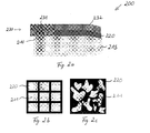
- Fig. 1 shows an embodiment of an epitaxial wafer 100 according to the first aspect of the invention.
- Fig. 1a shows the epitaxial wafer in a top view. In this view, a group-III-nitride buffer layer structure, which is shown in Fig. 1b is not yet deposited.
- Fig. 1a shows a center region 110 of the principle surface of the silicon substrate in the center region of the epitaxial wafer 100 and an edge-mask layer 120 on the edge region of the principle surface of the silicon substrate near an outer circumferential line of the principle surface.
- Fig. 1b shows a sectional view of an edge part of the epitaxial wafer 100 with the silicon substrate 115 on which in the edge region the edge-mask layer 120 is deposited.
- a group-III-nitride buffer layer 130 is deposited on the center region 110 of the principle surface of the silicon substrate as well as on the edge-mask layer 120.
- the group-III-nitride buffer layer structure 130 comprises in the shown embodiment a plurality of single group-III-nitride buffer layers. In other embodiments the group-III-nitride buffer layer structure can also comprise a single layer.
- the group-III-nitride buffer layer structure 130 comprises two section, a high quality section 131, which is grown on the center region 110 of the principle surface of the silicon substrate 115 and a strain-relief section 132, which is grown on the edge-mask layer 120.
- the strain-relief section 132 herein has a higher amount of crystallographic defects than the high quality section 131 of the group-III-nitride buffer layer structure 130.
- the strain-relief section with its higher amount of crystallographic defects inhibits the building of cracks in the high quality section by reducing the strain in the group-III-nitride buffer layer structure.
- the strain-relief section 132 can be considered as a sacrificial region, which is later sacrificed in order to improve the quality of the high quality region 131.
- the strain-relief section 132 can be considered as a sacrificial region, which is later sacrificed in order to improve the quality of the high quality region 131.
- Fig. 2 shows a second embodiment of an epitaxial wafer 200 according to the first aspect of the invention.
- Fig. 2a shows an edge part of the epitaxial wafer 200 in the sectional view.
- the second embodiment of the epitaxial wafer 200 differs from the first embodiment, shown in Fig. 1 , by the structuring of the edge-mask layer 220.
- the edge-mask layer 220 is micro-structured.
- the micro-structuring of the edge-mask layer 220 can be a regular pattern, as shown in Fig. 2b or an irregular pattern, i. e. build up by a self-assembled porous material, as shown in Fig. 2c .
- the Fig. 2b and 2c hereby show top view on a part of an uncovered edge-mask layer in two different embodiments.
- the edge-mask layer 220 shows regular openings, through which parts of the principle surface 211 of the silicon substrate 315 are exposed
- the material of the edge-mask layer 220 in this embodiment is a polycrystalline material.
- the edge-mask layer 220 comprises amorphous material.
- the edge-mask layer 220 is built from a self-assembled porous material, which shows irregular openings, through which parts of the principle surface 211 are exposed.
- the additional micro-structuring if regular or irregular, further improves the epitaxial wafer while inducing a higher amount of crystallographic defects in the strain-relief section 232 of the group-III-nitride buffer layer 230, grown on top of the edge-mask layer 220.
- the strain-relief section 232 is a polycrystalline section.
- the strain-relief section 232 is single crystalline, but has a higher defect density than the high quality section 231 of the group-III-nitride buffer layer.
- the high quality section of the group-III-nitride buffer layer is in all embodiments of the invention single crystalline.
- Fig. 3 shows an embodiment of an epitaxial wafer 300 according to a second aspect of the invention in a top view.
- the epitaxial wafer 300 according to the second aspect of the invention comprises an edge-mask layer not only in the edge region of the principle surface of the silicon substrate, but also as a patterned regular grid 325 that covers section of the center region 310 of the principle surface of the silicon substrate, such that remaining uncovered principle surface 311 of the silicon substrate and the edge-mask layer 220 comprising the grid 325 together form a growth substrate for a group-III-nitride buffer layer structure conformally deposited thereon.
- the patterned regular grid 325 additionally improves the strain-relief in the buffer layer structure grown on top of it.
- the patterned regular grid 325 is in one embodiment formed of a material, which is additionally micro-structured. This means, that the material can be either self-assembled porous or regularly patterned, wherein the patterning has a smaller substructure size than the grid itself.
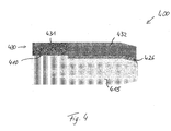
- Fig. 4 shows an embodiment of an epitaxial wafer 400 according to the third aspect of the invention.
- this embodiment of an epitaxial wafer 400 does not comprise a deposited edge-mask layer covering the edge region of the silicon substrate 415, but instead an edge mask 426, which comprises amorphous silicon formed from surface sections of the silicon substrate.
- the amorphous layer also induce polycrystalline growth or the growth of single crystalline strain-relief section 432 of group-III-nitride buffer layer structure on top of it, which has a higher amount of crystallographic defect than a high quality part 431 of the group-III-nitride buffer layer structure, which is grown directly on the center region 410 of principle surface of the silicon substrate.
- Fig. 5 shows a second embodiment of an epitaxial wafer 500 according the third aspect of the invention.
- the embodiment of Fig. 5 which is shown in a sectional view in Fig. 5a and in a top view on the edge mask 527 in Fig. 5b , comprises an edge mask 527 in form of a regular pattern, herein a grid.
- the edge mask is in this embodiment build up in the form of a regular pattern in the principle surface 211 of the silicon substrate 215, wherein a grid is formed by amorphous silicon in the silicon substrate.
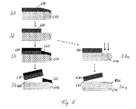
- Fig. 6 shows an embodiment of a method for forming an epitaxial wafer as a sequence of sectional views of an edge region of the wafer.
- a silicon substrate 610 is provided having a principle surface with a center region and an edge region near an outer circumferential line of the principle surface.
- a temporary fabrication mask layer 650 is deposited on the whole principle surface of the silicon substrate 615.
- the temporary fabrication mask layer is patterned.
- materials for the temporary fabrication mask layer i. e. photoresists or SiO 2 are advantageous.
- the patterning can i. e. be made by etching.
- the edge-mask layer 620 is deposited on the whole substrate.
- the edge-mask layer in this step covers the temporary fabrication mask 650 as well as the exposed parts of the principle surface of the substrate, which is in the shown embodiment the edge region of the substrate.
- the temporary fabrication mask 650 as well as the edge-mask layer covering the temporary fabrication mask are removed and the center region 610 of the principle surface of the silicon substrate is exposed.
- the group-III-nitride buffer layer structure is deposited on the epitaxial wafer 600.
- an alternative step S3A is performed instead of step S3.
- step S3A the exposed the silicon substrate is treated with plasma bombardment with plasma in order to form amorphous silicon of the exposed parts of the surface of the silicon substrate. Consequently, in step S4A only the temporary fabrication mask 650 is removed.
- Fig. 7 shows an alternative embodiment of a method for forming an epitaxial wafer 700 according to the first or the second aspect of the invention.
- the process in Fig. 7 uses a positive mask, which means instead of covering sections of the principle surface of the silicon substrate, which will be exposed in the last fabrication step, in the process of Fig. 7 the mask covers the remaining part of the edge-mask layer during the process of exposing the principle surface.
- the edge-mask layer 720 is deposited on the whole principle surface of the silicon substrate.
- step S12 a temporary fabrication mask is deposited on the edge region of the epitaxial wafer.
- step S13 the uncovered part of the edge-mask layer is removed and the center region 710 of the principle surface is exposed.
- step S14 the temporary fabrication mask 750 is removed and subsequent deposition of a group-III-nitride buffer layer is performed in further steps, not shown herein.
Landscapes
- Crystals, And After-Treatments Of Crystals (AREA)
- Recrystallisation Techniques (AREA)
Priority Applications (2)
| Application Number | Priority Date | Filing Date | Title |
|---|---|---|---|
| EP13191827.8A EP2945185A1 (fr) | 2013-11-06 | 2013-11-06 | Plaquettes épitaxiales évitant une gravure à refusion de bord et son procédé de fabrication |
| PCT/EP2014/073875 WO2015067681A1 (fr) | 2013-11-06 | 2014-11-06 | Plaquettes épitaxiales évitant une gravure à recristalliation de bord, et leur procédé de fabrication |
Applications Claiming Priority (1)
| Application Number | Priority Date | Filing Date | Title |
|---|---|---|---|
| EP13191827.8A EP2945185A1 (fr) | 2013-11-06 | 2013-11-06 | Plaquettes épitaxiales évitant une gravure à refusion de bord et son procédé de fabrication |
Publications (1)
| Publication Number | Publication Date |
|---|---|
| EP2945185A1 true EP2945185A1 (fr) | 2015-11-18 |
Family
ID=49553584
Family Applications (1)
| Application Number | Title | Priority Date | Filing Date |
|---|---|---|---|
| EP13191827.8A Withdrawn EP2945185A1 (fr) | 2013-11-06 | 2013-11-06 | Plaquettes épitaxiales évitant une gravure à refusion de bord et son procédé de fabrication |
Country Status (2)
| Country | Link |
|---|---|
| EP (1) | EP2945185A1 (fr) |
| WO (1) | WO2015067681A1 (fr) |
Cited By (1)
| Publication number | Priority date | Publication date | Assignee | Title |
|---|---|---|---|---|
| DE102019116743A1 (de) | 2018-06-22 | 2019-12-24 | X-Fab Semiconductor Foundries Gmbh | Substrate für Gruppe-III-Nitrid-Epitaxie |
Families Citing this family (2)
| Publication number | Priority date | Publication date | Assignee | Title |
|---|---|---|---|---|
| KR102608902B1 (ko) * | 2016-06-14 | 2023-12-04 | 삼성전자주식회사 | 질화물 반도체 기판 제조방법 |
| CN114695503A (zh) * | 2020-12-31 | 2022-07-01 | 联华电子股份有限公司 | 半导体结构 |
Citations (4)
| Publication number | Priority date | Publication date | Assignee | Title |
|---|---|---|---|---|
| US20020197841A1 (en) * | 2001-06-05 | 2002-12-26 | Seiji Nagai | Group III nitride compound semiconductor element and method for producing the same |
| EP1855309A1 (fr) * | 2005-02-28 | 2007-11-14 | Shin-Etsu Handotai Company Limited | Procédé de fabrication de galette collée et galette collée |
| US20130087807A1 (en) | 2010-06-25 | 2013-04-11 | Dowa Electronics Materials Co., Ltd. | Epitaxial growth substrate, semiconductor device, and epitaxial growth method |
| EP2602810A1 (fr) * | 2011-12-05 | 2013-06-12 | Samsung Electronics Co., Ltd. | Substrat de silicium, structure épitaxiale comprenant celui-ci et procédé de fabrication du substrat de silicium |
-
2013
- 2013-11-06 EP EP13191827.8A patent/EP2945185A1/fr not_active Withdrawn
-
2014
- 2014-11-06 WO PCT/EP2014/073875 patent/WO2015067681A1/fr not_active Ceased
Patent Citations (4)
| Publication number | Priority date | Publication date | Assignee | Title |
|---|---|---|---|---|
| US20020197841A1 (en) * | 2001-06-05 | 2002-12-26 | Seiji Nagai | Group III nitride compound semiconductor element and method for producing the same |
| EP1855309A1 (fr) * | 2005-02-28 | 2007-11-14 | Shin-Etsu Handotai Company Limited | Procédé de fabrication de galette collée et galette collée |
| US20130087807A1 (en) | 2010-06-25 | 2013-04-11 | Dowa Electronics Materials Co., Ltd. | Epitaxial growth substrate, semiconductor device, and epitaxial growth method |
| EP2602810A1 (fr) * | 2011-12-05 | 2013-06-12 | Samsung Electronics Co., Ltd. | Substrat de silicium, structure épitaxiale comprenant celui-ci et procédé de fabrication du substrat de silicium |
Cited By (3)
| Publication number | Priority date | Publication date | Assignee | Title |
|---|---|---|---|---|
| DE102019116743A1 (de) | 2018-06-22 | 2019-12-24 | X-Fab Semiconductor Foundries Gmbh | Substrate für Gruppe-III-Nitrid-Epitaxie |
| DE102019116743B4 (de) | 2018-06-22 | 2025-02-27 | X-Fab Semiconductor Foundries Gmbh | Verfahren zur Herstellung eines Wafers für Gruppe-III-Nitrid-Epitaxie |
| US12331426B2 (en) | 2018-06-22 | 2025-06-17 | X-Fab Semiconductor Foundries Gmbh | Substrates for III-nitride epitaxy |
Also Published As
| Publication number | Publication date |
|---|---|
| WO2015067681A1 (fr) | 2015-05-14 |
Similar Documents
| Publication | Publication Date | Title |
|---|---|---|
| US9233844B2 (en) | Graded aluminum—gallium—nitride and superlattice buffer layer for III-V nitride layer on silicon substrate | |
| JP6425835B2 (ja) | ダイヤモンド−半導体複合基板を製造する方法 | |
| JP4741572B2 (ja) | 窒化物半導体基板及びその製造方法 | |
| KR102827297B1 (ko) | 질화갈륨/다이아몬드 웨이퍼 | |
| EP3890000B1 (fr) | Procédé de fabrication de substrat en diamant | |
| CN103137656A (zh) | 硅衬底及其制造方法和外延结构及其制造方法 | |
| KR101878754B1 (ko) | 대면적 갈륨 나이트라이드 기판 제조방법 | |
| JP5371430B2 (ja) | 半導体基板並びにハイドライド気相成長法により自立半導体基板を製造するための方法及びそれに使用されるマスク層 | |
| TWI604094B (zh) | 半導體磊晶晶圓的製造方法及半導體磊晶晶圓 | |
| CN103489896B (zh) | 氮化镓基半导体器件及其制造方法 | |
| KR102680861B1 (ko) | 질화 갈륨 기판의 제조 방법 | |
| EP2945185A1 (fr) | Plaquettes épitaxiales évitant une gravure à refusion de bord et son procédé de fabrication | |
| CN107978659B (zh) | 制造氮化镓衬底的方法 | |
| TWI750847B (zh) | 半導體晶圓及其製造方法 | |
| US20190035628A1 (en) | Method and structure for reducing substrate fragility | |
| KR101635530B1 (ko) | 다수의 공극을 갖는 질화물 반도체 결정 성장 방법 및 이를 이용한 질화물 반도체 기판 제조 방법 | |
| US11450747B2 (en) | Semiconductor structure with an epitaxial layer | |
| KR20190052000A (ko) | 단결정 반도체 섬들을 포함하는 구조물 및 그러한 구조물의 제조 방법 | |
| KR102262063B1 (ko) | 에피택셜 웨이퍼의 제조방법 및 에피택셜 성장용 실리콘계 기판 | |
| JP7647446B2 (ja) | 窒化物半導体基板及びその製造方法 | |
| KR102757670B1 (ko) | 다이아몬드가 성장된 soi 템플레이트 및 단결정 다이아몬드 제조 방법 | |
| US9779935B1 (en) | Semiconductor substrate with stress relief regions |
Legal Events
| Date | Code | Title | Description |
|---|---|---|---|
| PUAI | Public reference made under article 153(3) epc to a published international application that has entered the european phase |
Free format text: ORIGINAL CODE: 0009012 |
|
| AK | Designated contracting states |
Kind code of ref document: A1 Designated state(s): AL AT BE BG CH CY CZ DE DK EE ES FI FR GB GR HR HU IE IS IT LI LT LU LV MC MK MT NL NO PL PT RO RS SE SI SK SM TR |
|
| AX | Request for extension of the european patent |
Extension state: BA ME |
|
| STAA | Information on the status of an ep patent application or granted ep patent |
Free format text: STATUS: THE APPLICATION IS DEEMED TO BE WITHDRAWN |
|
| 18D | Application deemed to be withdrawn |
Effective date: 20160519 |