EP2945187A1 - Kristallschichtstruktur und lichtemittierendes element - Google Patents
Kristallschichtstruktur und lichtemittierendes element Download PDFInfo
- Publication number
- EP2945187A1 EP2945187A1 EP13870949.8A EP13870949A EP2945187A1 EP 2945187 A1 EP2945187 A1 EP 2945187A1 EP 13870949 A EP13870949 A EP 13870949A EP 2945187 A1 EP2945187 A1 EP 2945187A1
- Authority
- EP
- European Patent Office
- Prior art keywords
- substrate
- layer
- nitride semiconductor
- dielectric layer
- layered structure
- Prior art date
- Legal status (The legal status is an assumption and is not a legal conclusion. Google has not performed a legal analysis and makes no representation as to the accuracy of the status listed.)
- Withdrawn
Links
Images




Classifications
-
- H—ELECTRICITY
- H10—SEMICONDUCTOR DEVICES; ELECTRIC SOLID-STATE DEVICES NOT OTHERWISE PROVIDED FOR
- H10H—INORGANIC LIGHT-EMITTING SEMICONDUCTOR DEVICES HAVING POTENTIAL BARRIERS
- H10H20/00—Individual inorganic light-emitting semiconductor devices having potential barriers, e.g. light-emitting diodes [LED]
- H10H20/80—Constructional details
- H10H20/81—Bodies
- H10H20/819—Bodies characterised by their shape, e.g. curved or truncated substrates
- H10H20/82—Roughened surfaces, e.g. at the interface between epitaxial layers
-
- H—ELECTRICITY
- H10—SEMICONDUCTOR DEVICES; ELECTRIC SOLID-STATE DEVICES NOT OTHERWISE PROVIDED FOR
- H10H—INORGANIC LIGHT-EMITTING SEMICONDUCTOR DEVICES HAVING POTENTIAL BARRIERS
- H10H20/00—Individual inorganic light-emitting semiconductor devices having potential barriers, e.g. light-emitting diodes [LED]
- H10H20/80—Constructional details
- H10H20/81—Bodies
- H10H20/817—Bodies characterised by the crystal structures or orientations, e.g. polycrystalline, amorphous or porous
- H10H20/818—Bodies characterised by the crystal structures or orientations, e.g. polycrystalline, amorphous or porous within the light-emitting regions
-
- H—ELECTRICITY
- H10—SEMICONDUCTOR DEVICES; ELECTRIC SOLID-STATE DEVICES NOT OTHERWISE PROVIDED FOR
- H10H—INORGANIC LIGHT-EMITTING SEMICONDUCTOR DEVICES HAVING POTENTIAL BARRIERS
- H10H20/00—Individual inorganic light-emitting semiconductor devices having potential barriers, e.g. light-emitting diodes [LED]
- H10H20/80—Constructional details
- H10H20/81—Bodies
- H10H20/822—Materials of the light-emitting regions
- H10H20/824—Materials of the light-emitting regions comprising only Group III-V materials, e.g. GaP
- H10H20/825—Materials of the light-emitting regions comprising only Group III-V materials, e.g. GaP containing nitrogen, e.g. GaN
-
- H—ELECTRICITY
- H10—SEMICONDUCTOR DEVICES; ELECTRIC SOLID-STATE DEVICES NOT OTHERWISE PROVIDED FOR
- H10P—GENERIC PROCESSES OR APPARATUS FOR THE MANUFACTURE OR TREATMENT OF DEVICES COVERED BY CLASS H10
- H10P14/00—Formation of materials, e.g. in the shape of layers or pillars
- H10P14/20—Formation of materials, e.g. in the shape of layers or pillars of semiconductor materials
- H10P14/27—Formation of materials, e.g. in the shape of layers or pillars of semiconductor materials using selective deposition, e.g. simultaneous growth of monocrystalline and non-monocrystalline semiconductor materials
- H10P14/271—Formation of materials, e.g. in the shape of layers or pillars of semiconductor materials using selective deposition, e.g. simultaneous growth of monocrystalline and non-monocrystalline semiconductor materials characterised by the preparation of substrate for selective deposition
-
- H—ELECTRICITY
- H10—SEMICONDUCTOR DEVICES; ELECTRIC SOLID-STATE DEVICES NOT OTHERWISE PROVIDED FOR
- H10P—GENERIC PROCESSES OR APPARATUS FOR THE MANUFACTURE OR TREATMENT OF DEVICES COVERED BY CLASS H10
- H10P14/00—Formation of materials, e.g. in the shape of layers or pillars
- H10P14/20—Formation of materials, e.g. in the shape of layers or pillars of semiconductor materials
- H10P14/29—Formation of materials, e.g. in the shape of layers or pillars of semiconductor materials characterised by the substrates
- H10P14/2901—Materials
- H10P14/2918—Materials being semiconductor metal oxides
-
- H—ELECTRICITY
- H10—SEMICONDUCTOR DEVICES; ELECTRIC SOLID-STATE DEVICES NOT OTHERWISE PROVIDED FOR
- H10P—GENERIC PROCESSES OR APPARATUS FOR THE MANUFACTURE OR TREATMENT OF DEVICES COVERED BY CLASS H10
- H10P14/00—Formation of materials, e.g. in the shape of layers or pillars
- H10P14/20—Formation of materials, e.g. in the shape of layers or pillars of semiconductor materials
- H10P14/29—Formation of materials, e.g. in the shape of layers or pillars of semiconductor materials characterised by the substrates
- H10P14/2926—Crystal orientations
-
- H—ELECTRICITY
- H10—SEMICONDUCTOR DEVICES; ELECTRIC SOLID-STATE DEVICES NOT OTHERWISE PROVIDED FOR
- H10P—GENERIC PROCESSES OR APPARATUS FOR THE MANUFACTURE OR TREATMENT OF DEVICES COVERED BY CLASS H10
- H10P14/00—Formation of materials, e.g. in the shape of layers or pillars
- H10P14/20—Formation of materials, e.g. in the shape of layers or pillars of semiconductor materials
- H10P14/32—Formation of materials, e.g. in the shape of layers or pillars of semiconductor materials characterised by intermediate layers between substrates and deposited layers
- H10P14/3202—Materials thereof
- H10P14/3238—Materials thereof being insulating materials
-
- H—ELECTRICITY
- H10—SEMICONDUCTOR DEVICES; ELECTRIC SOLID-STATE DEVICES NOT OTHERWISE PROVIDED FOR
- H10P—GENERIC PROCESSES OR APPARATUS FOR THE MANUFACTURE OR TREATMENT OF DEVICES COVERED BY CLASS H10
- H10P14/00—Formation of materials, e.g. in the shape of layers or pillars
- H10P14/20—Formation of materials, e.g. in the shape of layers or pillars of semiconductor materials
- H10P14/32—Formation of materials, e.g. in the shape of layers or pillars of semiconductor materials characterised by intermediate layers between substrates and deposited layers
- H10P14/3242—Structure
-
- H—ELECTRICITY
- H10—SEMICONDUCTOR DEVICES; ELECTRIC SOLID-STATE DEVICES NOT OTHERWISE PROVIDED FOR
- H10P—GENERIC PROCESSES OR APPARATUS FOR THE MANUFACTURE OR TREATMENT OF DEVICES COVERED BY CLASS H10
- H10P14/00—Formation of materials, e.g. in the shape of layers or pillars
- H10P14/20—Formation of materials, e.g. in the shape of layers or pillars of semiconductor materials
- H10P14/34—Deposited materials, e.g. layers
- H10P14/3402—Deposited materials, e.g. layers characterised by the chemical composition
- H10P14/3414—Deposited materials, e.g. layers characterised by the chemical composition being group IIIA-VIA materials
- H10P14/3416—Nitrides
-
- H—ELECTRICITY
- H10—SEMICONDUCTOR DEVICES; ELECTRIC SOLID-STATE DEVICES NOT OTHERWISE PROVIDED FOR
- H10P—GENERIC PROCESSES OR APPARATUS FOR THE MANUFACTURE OR TREATMENT OF DEVICES COVERED BY CLASS H10
- H10P14/00—Formation of materials, e.g. in the shape of layers or pillars
- H10P14/20—Formation of materials, e.g. in the shape of layers or pillars of semiconductor materials
- H10P14/34—Deposited materials, e.g. layers
- H10P14/3466—Crystal orientation
-
- C—CHEMISTRY; METALLURGY
- C30—CRYSTAL GROWTH
- C30B—SINGLE-CRYSTAL GROWTH; UNIDIRECTIONAL SOLIDIFICATION OF EUTECTIC MATERIAL OR UNIDIRECTIONAL DEMIXING OF EUTECTOID MATERIAL; REFINING BY ZONE-MELTING OF MATERIAL; PRODUCTION OF A HOMOGENEOUS POLYCRYSTALLINE MATERIAL WITH DEFINED STRUCTURE; SINGLE CRYSTALS OR HOMOGENEOUS POLYCRYSTALLINE MATERIAL WITH DEFINED STRUCTURE; AFTER-TREATMENT OF SINGLE CRYSTALS OR A HOMOGENEOUS POLYCRYSTALLINE MATERIAL WITH DEFINED STRUCTURE; APPARATUS THEREFOR
- C30B29/00—Single crystals or homogeneous polycrystalline material with defined structure characterised by the material or by their shape
- C30B29/10—Inorganic compounds or compositions
- C30B29/16—Oxides
-
- C—CHEMISTRY; METALLURGY
- C30—CRYSTAL GROWTH
- C30B—SINGLE-CRYSTAL GROWTH; UNIDIRECTIONAL SOLIDIFICATION OF EUTECTIC MATERIAL OR UNIDIRECTIONAL DEMIXING OF EUTECTOID MATERIAL; REFINING BY ZONE-MELTING OF MATERIAL; PRODUCTION OF A HOMOGENEOUS POLYCRYSTALLINE MATERIAL WITH DEFINED STRUCTURE; SINGLE CRYSTALS OR HOMOGENEOUS POLYCRYSTALLINE MATERIAL WITH DEFINED STRUCTURE; AFTER-TREATMENT OF SINGLE CRYSTALS OR A HOMOGENEOUS POLYCRYSTALLINE MATERIAL WITH DEFINED STRUCTURE; APPARATUS THEREFOR
- C30B29/00—Single crystals or homogeneous polycrystalline material with defined structure characterised by the material or by their shape
- C30B29/10—Inorganic compounds or compositions
- C30B29/40—AIIIBV compounds wherein A is B, Al, Ga, In or Tl and B is N, P, As, Sb or Bi
- C30B29/403—AIII-nitrides
-
- H—ELECTRICITY
- H10—SEMICONDUCTOR DEVICES; ELECTRIC SOLID-STATE DEVICES NOT OTHERWISE PROVIDED FOR
- H10H—INORGANIC LIGHT-EMITTING SEMICONDUCTOR DEVICES HAVING POTENTIAL BARRIERS
- H10H20/00—Individual inorganic light-emitting semiconductor devices having potential barriers, e.g. light-emitting diodes [LED]
- H10H20/01—Manufacture or treatment
- H10H20/011—Manufacture or treatment of bodies, e.g. forming semiconductor layers
- H10H20/013—Manufacture or treatment of bodies, e.g. forming semiconductor layers having light-emitting regions comprising only Group III-V materials
- H10H20/0133—Manufacture or treatment of bodies, e.g. forming semiconductor layers having light-emitting regions comprising only Group III-V materials with a substrate not being Group III-V materials
- H10H20/01335—Manufacture or treatment of bodies, e.g. forming semiconductor layers having light-emitting regions comprising only Group III-V materials with a substrate not being Group III-V materials the light-emitting regions comprising nitride materials
Definitions
- the invention relates to a crystal layered structure and a light emitting element.
- a crystal film is grown on a rugged surface of a translucent substrate (see, e.g., PTL 1).
- PTL 1 a GaN-based semiconductor layer is grown on a rugged surface of a sapphire substrate.
- the rugged pattern of the sapphire substrate in PTL 1 has a function of suppressing reflection of light emitted from a light-emitting layer in the GaN-based semiconductor layer, which occurs at an interface between the sapphire substrate and the GaN-based semiconductor layer due to a difference in refractive index between the sapphire substrate and the GaN-based semiconductor layer. Suppression of such reflection allows absorption of the reflected light by the light-emitting layer and attenuation of the reflected light due to multiple reflection to be reduced, thereby improving light extraction efficiency of the light emitting element.
- a crystal layered structure set forth in [1] to [5] below is provided so as to achieve the object.
- a crystal layered structure can be provided that includes a Ga 2 O 3 substrate and a nitride semiconductor layer so as to have a light emitting element with a high light output, as well as a light emitting element including the crystal layered structure.
- a method for forming a crystal layered structure having a Ga 2 O 3 substrate and a nitride semiconductor layer, a method may be devised in which a rugged pattern is formed on a surface of the Ga 2 O 3 substrate and a nitride semiconductor crystal is then grown thereon for the purpose of reducing light reflection which occurs at an interface between the Ga 2 O 3 substrate and the nitride semiconductor layer due to a difference in refractive index between the Ga 2 O 3 substrate and the nitride semiconductor layer.
- the inventors have found that when growing a nitride semiconductor crystal on a rugged surface of the Ga 2 O 3 substrate, the obtained nitride semiconductor layer does not have high crystal quality.
- the Ga 2 O 3 substrate has only limited crystal planes which allow a high-quality nitride semiconductor crystal to be grown.
- various crystal planes including those unsuitable as a base for growing a high-quality nitride semiconductor crystal are formed and a nitride semiconductor layer with high crystal quality is thus not obtained.
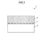
- FIG.1 is a vertical cross-sectional view showing a crystal layered structure in the first embodiment.
- a crystal layered structure 1 includes a Ga 2 O 3 substrate 2, a dielectric layer 3 on the Ga 2 O 3 substrate 2 and a nitride semiconductor layer 4 on the dielectric layer 3.
- the Ga 2 O 3 substrate 2 is formed of a ⁇ -Ga 2 O 3 single crystal.
- the upper surface of the Ga 2 O 3 substrate 2 is a flat surface without rugged pattern and is oriented to (101), (-201) or (100), etc., which can provide a base for growing a high-quality nitride semiconductor crystal.
- a refractive index of the Ga 2 O 3 substrate 2 is about 1.9.
- the dielectric layer 3 is a layer having a refractive index difference of not more than 0.15 relative to the Ga 2 O 3 substrate 2 and is, e.g., a SiN layer consisting mainly of SiN or an HfO 2 layer consisting mainly of HfO 2 . If the refractive index of the Ga 2 O 3 substrate 2 is e.g. 1.9, the refractive index of the dielectric layer 3 is to be not less than 1.75 and not more than 2.05.
- the dielectric layer 3 is formed on the Ga 2 O 3 substrate 2 so as to partially cover the upper surface of the Ga 2 O 3 substrate 2.
- the pattern shape of the dielectric layer 3 is not limited and is, e.g., a dot pattern, a hole pattern or a line-and-space pattern.
- the SiN layer provided as the dielectric layer 3 may contain elements other than Si and N, such as O, but is preferably formed of substantially only SiN to further reduce a difference between the refractive index of the dielectric layer 3 and that of the Ga 2 O 3 substrate 2.
- the refractive index of the dielectric layer 3 is preferably not more than that of the Ga 2 O 3 substrate 2 so that total reflection of light traveling from the dielectric layer 3 toward the Ga 2 O 3 substrate 2 is prevented.
- the refractive index of the dielectric layer 3 can be adjusted by controlling the conditions for forming the dielectric layer 3, such as film-forming temperature, to reduce the difference between the refractive index of the dielectric layer 3 and that of the Ga 2 O 3 substrate 2.
- the SiO 2 layer has a refractive index of about 1.5 to 1.6 and thus has the refractive index difference of not less than 0.3 relative to the Ga 2 O 3 substrate 2.
- the nitride semiconductor layer 4 may have a multilayer structure in which plural layers formed of different nitride semiconductor crystals are laminated.
- the crystal layered structure 1 is used to form, e.g., a light emitting element, cladding layers and a light-emitting layer sandwiched therebetween, etc., may be included in the nitride semiconductor layer 4.
- the Ga 2 O 3 substrate 2 and the nitride semiconductor layer 4 may contain a conductive impurity such as Si.
- the dielectric layer 3 does not entirely cover the upper surface of the Ga 2 O 3 substrate 2.
- the nitride semiconductor layer 4 is in contact with the dielectric layer 3 as well as the upper surface of the Ga 2 O 3 substrate 2 at a portion not covered by the dielectric layer 3.
- a nitride semiconductor crystal constituting the nitride semiconductor layer 4 is grown from the upper surface of the Ga 2 O 3 substrate 2 in a region not covered by the dielectric layer 3, and is not grown from the dielectric layer 3. Since the nitride semiconductor layer 4 is formed by such selective growth of the nitride semiconductor crystal, dislocation density in the nitride semiconductor layer 4 is reduced and crystal quality is thus improved.
- the crystal growth method using such selective growth is called ELO (Epitaxial Lateral Overgrowth), etc.
- the thickness of the dielectric layer 3 for improving transmittance is determined according to a wavelength of light incident on the dielectric layer 3 from the nitride semiconductor layer 4.
- the thickness of the dielectric layer 3 is desirably greater than the wavelength.
- the thickness of the dielectric layer 3 is preferably not less than 0.5 ⁇ m.
- a manufacturing process when using a SiN layer as the dielectric layer 3 will be described below as an example of the process of manufacturing the crystal layered structure in the present embodiment.
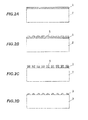
- FIGS.2A to 2D are vertical cross-sectional views showing a process of manufacturing the crystal layered structure in the first embodiment.
- the Ga 2 O 3 substrate 2 treated by CMP is subjected to organic cleaning, SPM (Sulfuric acid/hydrogen peroxide mixture) cleaning and HF solution cleaning.
- the Ga 2 O 3 substrate 2 is transferred to a chamber of a MOCVD (Metal Organic Chemical Vapor Deposition) system.
- MOCVD Metal Organic Chemical Vapor Deposition
- the dielectric layer 3 in the form of film is formed on the Ga 2 O 3 substrate 2.
- SiN is deposited on the Ga 2 O 3 substrate 2 by supplying SiH 4 as a Si raw material, NH 3 gas as an N raw material and N 2 gas as an atmosphere gas into the chamber in a state that the temperature in the chamber is maintained at 300 to 350°C, thereby forming the dielectric layer 3 in the form of film.
- the dielectric layer 3 is a film having a substantially uniform thickness of about 1 ⁇ m.
- the raw materials of the respective elements are not limited to those mentioned above.
- a resist pattern 5 is formed on the dielectric layer 3.
- the pattern shape of the resist pattern 5 is, e.g., a dot pattern with 2 ⁇ m-diameter dots at a pitch of 3 ⁇ m, but may be another pattern such as hole pattern or line-and-space pattern.
- the resist pattern 5 is formed by, e.g., photolithography.
- the dielectric layer 3 is etched with BHF (buffered hydrofluoric acid) using the resist pattern 5 as a mask, thereby transferring the pattern of the resist pattern 5 to the dielectric layer 3.
- BHF buffered hydrofluoric acid
- an AI x Ga y In z N crystal as a nitride semiconductor crystal is selectively grown on the Ga 2 O 3 substrate 2 by supplying NH 3 gas as an N raw material, trimethylgallium (TMG) gas as a Ga raw material, trimethylaluminum (TMA) gas as an A1 raw material and trimethylindium (TMI) gas as an In raw material into the chamber, thereby forming the nitride semiconductor layer 4.
- TMG trimethylgallium
- TMA trimethylaluminum
- TMI trimethylindium
- the nitride semiconductor layer 4 is composed of a buffer layer formed of an AlGaInN crystal and a GaN layer thereon.
- the surface of a structure composed of the Ga 2 O 3 substrate 2 and the dielectric layer 3 is cleaned by organic cleaning and SPM cleaning and the structure is introduced into the MOCVD system.
- NH 3 gas as an N raw material
- trimethylgallium (TMG) as a Ga raw material
- trimethylaluminum (TMA) as an Al raw material
- TMI trimethylindium
- Si Si as an n-type impurity
- the temperature of the substrate surface is increased to around 1000°C to form an initial n-GaN core which is then continuously grown to about 2 ⁇ m. Then, a 2 ⁇ m-thick n-GaN layer is formed at an elevated substrate surface temperature of around 1100°C, thereby obtaining the nitride semiconductor layer 4.
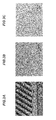
- FIG.3A is a SEM (Scanning Electron Microscope) image showing the crystal layered structure in the first embodiment before formation of a nitride semiconductor layer
- FIGS.3B and 3C are SEM images after formation of the nitride semiconductor layer.
- FIG.3A shows the Ga 2 O 3 substrate 2 and a SiN layer as the dielectric layer 3
- FIGS.3B and 3C show a GaN layer having an upper surface oriented to (002) as the nitride semiconductor layer 4.
- FIG.4A is a SEM image showing the crystal layered structure in Comparative Example before formation of a nitride semiconductor layer
- FIGS.4B and 4C are SEM images after formation of the nitride semiconductor layer.
- FIG.4A shows the Ga 2 O 3 substrate 2 with a rugged upper surface
- FIGS.4B and 4C show a GaN layer having an upper surface oriented to (002) which is a layer corresponding to the nitride semiconductor layer 4 in the present embodiment.
- FIGS.3A and 4A are images of the upper surface of the Ga 2 O 3 substrate 2 taken from obliquely above.
- Truncated cone-shaped objects in FIG.3A are a dot-patterned SiN constituting the dielectric layer 3.
- Truncated cone-shaped objects in FIG.4A are raised portions on the dot-patterned upper surface of the Ga 2 O 3 substrate 2.
- FIGS.3B and 3C show that the upper surface of the nitride semiconductor layer 4 in the present embodiment is flat and the nitride semiconductor layer 4 has high crystal quality.
- dark areas shown in FIGS.4B and 4C are abnormally-grown portions of the crystal and it is understood that the nitride semiconductor layer in Comparative Example has poor crystal quality.
- This result shows that a nitride semiconductor layer with high crystal quality is obtained without abnormal growth by forming the dielectric layer 3 on a flat upper surface of the Ga 2 O 3 substrate 2, not by forming a rugged pattern on the upper surface of the Ga 2 O 3 substrate 2.
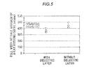
- FIG.5 is a graph showing FWHMs of x-ray rocking curves from the nitride semiconductor layer of the crystal layered structure in the first embodiment and those in Comparative Example.
- the crystal layered structure in Comparative Example shown in FIG.5 does not include the dielectric layer 3 and is composed of only the Ga 2 O 3 substrate 2 and a nitride semiconductor layer.
- the dielectric layer 3 in the first embodiment which is used for measurement pertaining to FIG.5 is a SiN layer. Meanwhile, both the nitride semiconductor layer 4 in the first embodiment and the nitride semiconductor layer in Comparative Example are formed of a GaN crystal and have an upper surface oriented to (002).
- the measured values of the crystal layered structure 1 in the first embodiment are indicated on the left side above “with dielectric layer” and the measured values of the crystal layered structure in Comparative Example are indicated on the right side above "without dielectric layer”.
- FWHM of x-ray rocking curve from a (002) plane and that from a (101) plane perpendicular to the (002) plane are respectively indicated by " ⁇ (open square)” and “ ⁇ (open diamond)".
- FWHM of x-ray rocking curve from the (002) plane is to evaluate orientation of a plane parallel to the upper surface of the nitride semiconductor layer
- FWHM of x-ray rocking curve from the (101) plane is to evaluate orientation of a plane perpendicular to the upper surface of the nitride semiconductor layer.
- both FWHM of x-ray rocking curve from the (002) plane and that from the (101) plane are narrower in the crystal layered structure 1 having the dielectric layer 3 in the first embodiment than in the crystal layered structure not having the dielectric layer 3 in Comparative Example, especially remarkable in the results from the (101) plane.
- This result shows that crystal quality of the nitride semiconductor layer is improved by providing the dielectric layer 3.
- FIG.6 is a graph showing vertical current-voltage characteristics of the crystal layered structures in the first embodiment and Comparative Example when a dielectric layer is a SiN layer.
- the horizontal axis indicates voltage (V) and the vertical axis indicates current density (A/cm 2 ).
- the dielectric layer 3 in the first embodiment which is used for measurement pertaining to FIG.6 is a SiN layer. It has been confirmed that the crystal layered structure 1 has particularly excellent vertical current-voltage characteristics when the dielectric layer 3 is a SiN layer.
- the crystal layered structure in Comparative Example shown in FIG.6 does not include the dielectric layer 3 formed of SiN and is composed of only a Ga 2 O 3 substrate and a nitride semiconductor layer. Meanwhile, both the nitride semiconductor layer 4 in the first embodiment and the nitride semiconductor layer in Comparative Example are formed of a GaN crystal and have an upper surface oriented to (002).
- the measured values of the crystal layered structure 1 in the first embodiment are indicated by “with SiN layer” and the measured values of the crystal layered structure in Comparative Example are indicated by "without SiN layer”.
- FIG.6 shows a state in which electrodes are connected to the Ga 3 O 3 substrate 2 and the nitride semiconductor layer 4 of the crystal layered structure 1. Electrodes 6a and 6b were respectively connected to the Ga 2 O 3 substrate 2 and the nitride semiconductor layer 4. Electrodes were also connected to the crystal layered structure in Comparative Example in the same manner.
- FIG.6 shows that a potential barrier is present at an interface between the Ga 2 O 3 substrate 2 and the nitride semiconductor layer in the crystal layered structure not having the dielectric layer 3 formed of SiN in Comparative Example while, in the crystal layered structure 1 having the dielectric layer 3 formed of SiN in the first embodiment, a potential barrier is not present at an interface between the Ga 2 O 3 substrate 2 and the nitride semiconductor layer 4 and the Ga 2 O 3 substrate 2 is in ohmic contact with the nitride semiconductor layer 4.
- This result shows that vertical electrical resistance of the crystal layered structure 1 is reduced by providing the dielectric layer 3 formed of SiN.
- the dielectric layer 3 formed of SiN in the first embodiment used for the images and the measurements of FIGS.3 , 5 and 6 was formed by a plasma CVD system (PD-220, manufactured by SAMCO Inc.) at a film-forming temperature of 300°C using SiH 4 gas, NH 3 gas and N 2 gas as process gases, and had a refractive index of 1.89.
- PD-220 manufactured by SAMCO Inc.
- the nitride semiconductor layer 4 is formed on the upper surface of the Ga 2 O 3 substrate 2 having the dielectric layer 3 formed thereon, it is possible to improve transmittance of light between the nitride semiconductor layer 4 and the Ga 2 O 3 substrate 2. In addition, it is possible to improve crystal quality of the nitride semiconductor layer 4. And, especially when the dielectric layer 3 is a SiN layer, it is possible to form an ohmic contact between the Ga 2 O 3 substrate 2 and the nitride semiconductor layer 4. Furthermore, in the present embodiment, it is possible to obtain improved crystal quality when a GaN layer is used as the nitride semiconductor layer 4.
- the second embodiment is an embodiment of a light emitting element including the crystal layered structure 1 in the first embodiment.
- An example of the light emitting element will be described below.
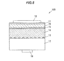
- FIG.8 is a vertical cross-sectional view showing a light emitting element in the second embodiment.
- a light emitting element 100 is an LED element which has a Ga 2 O 3 substrate 12, a dielectric layer 13 on the Ga 2 O 3 substrate 12, an n-type cladding layer 14 on the dielectric layer 13, a light-emitting layer 15 on the n-type cladding layer 14, a p-type cladding layer 16 on the light-emitting layer 15, a contact layer 17 on the p-type cladding layer 16, a p-type electrode 18 on the contact layer 17 and an n-type electrode 19 on a surface of the Ga 2 O 3 substrate 12 opposite to the dielectric layer 13.
- the Ga 2 O 3 substrate 12 and the dielectric layer 13 respectively correspond to the Ga 2 O 3 substrate 2 and the dielectric layer 3 in the first embodiment.
- the n-type cladding layer 14 is formed of a nitride semiconductor crystal. Therefore, at least the n-typc cladding layer 14 corresponds to the nitride semiconductor layer 4 in the first embodiment. In case that a layer(s) on the n-type cladding layer 14 is formed of a nitride semiconductor crystal, the n-type cladding layer 14 and the nitride semiconductor crystal layer(s) thereon correspond to the nitride semiconductor layer 4.
- the n-type cladding layer 14 When, e.g., the n-type cladding layer 14, the light-emitting layer 15, the p-type cladding layer 16 and the contact layer 17 are formed of a nitride semiconductor crystal, all of these layers correspond to the nitride semiconductor layer 4.
- the light emitting element 100 is a vertical light emitting element in which electricity is conducted to the Ga 2 O 3 substrate 12 and the above-mentioned layer(s) corresponding to the nitride semiconductor layer 4 during operation.
- the light emitting element 100 which is formed using the crystal layered structure 1 in the first embodiment, transmittance of light is high between the Ga 2 O 3 substrate 12 corresponding to the Ga 2 O 3 substrate 2 and the layers including the n-type cladding layer 14 and corresponding to the nitride semiconductor layer 4. Therefore, when the light emitting element 100 is a face-down type light emitting element configured to extract light from the Ga 2 O 3 substrate 12 side, light emitted from the light-emitting layer 15 and traveling toward the Ga 2 O 3 substrate 12 is efficiently transmitted, allowing high light output to be obtained.
- the light emitting element 100 is a face-up type light emitting element configured to extract light from the contact layer 17 side, it is possible to suppress reflection of light, which is emitted from the light-emitting layer 15 and traveling toward the Ga 2 O 3 substrate 12, at an interface between the n-type cladding layer 14 and the Ga 2 O 3 substrate 12 and absorption of such light by the light-emitting layer 15, etc. As a result, it is possible to obtain high light output.
- the Ga 2 O 3 substrate 12 is a 400 ⁇ m-thick n-type ⁇ -Ga 2 O 3 substrate having an upper surface oriented to (-201).
- the dielectric layer 13 is a 1 ⁇ m-thick SiN layer having a refractive index of 1.89 and covering 15% of the upper surface of the Ga 2 O 3 substrate 12 in a region immediately under the n-type cladding layer 14.
- the n-type cladding layer 14 is a 6 ⁇ m-thick n-type GaN crystal film.
- the light-emitting layer 15 is a layer composed of seven layers of 2.8 nm GaN crystal films and seven layers of 12 nm-thick InGaN crystal films which are alternately laminated.
- the p-type cladding layer 16 is a 0.2 ⁇ m-thick p-type GaN crystal film.
- the contact layer 17 is a 0.15 ⁇ m-thick p-type GaN crystal film.
- the configuration of the light emitting element in Comparative Example is basically the same as the light emitting element 100 but the dielectric layer 13 is not provided.
- FIG.9 is a graph showing vertical current-voltage characteristics of the light emitting elements in the second embodiment and Comparative Example when a dielectric layer is a SiN layer.
- the horizontal axis indicates voltage (V) and the vertical axis indicates current (m/A).
- the dielectric layer 13 in the second embodiment which is used for measurement pertaining to FIG.9 is a SiN layer. It has been confirmed that the light emitting element 100 has particularly excellent vertical current-voltage characteristics when the dielectric layer 13 is a SiN layer.
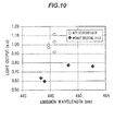
- FIG.10 is a graph showing light output characteristics of the light emitting elements in the second embodiment and Comparative Example.
- the horizontal axis indicates emission wavelength (nm) and the vertical axis indicates light output (arbitrary unit).
- the p-type electrode 18 side of the light emitting element 100 was attached to a mount and total luminous flux was measured.
- FIG.10 shows that light output from the light emitting element 100 having the dielectric layer 13 in the present embodiment is larger than that from light emitting element not having the dielectric layer 13 in Comparative Example. This result shows that it is possible to improve light output of the light emitting element by providing the dielectric layer 13.
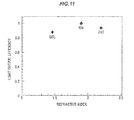
- FIG.11 is a graph obtained based on optical simulations and showing an example of a relation between a material of the dielectric layer and light extraction efficiency of the light emitting element.
- the Ga 2 O 3 substrate 12 had a refractive index of 1.9
- a dielectric layer corresponding to the dielectric layer 13 had a dot pattern with dots of 2 ⁇ m in diameter and 1 ⁇ m in height at a pitch of 3 ⁇ m
- light emitted from the light-emitting layer was extracted from the Ga 2 O 3 substrate 12 side.
- the reference light extraction efficiency in FIG.11 is light extraction efficiency when the light emitting element 100 in the present embodiment does not have the dielectric layer 13 but has the same rugged shape on the surface of the Ga 2 O 3 substrate 12.
- the light extraction efficiency used as a reference is a theoretical value when assuming that the n-type cladding layer 14, the light-emitting layer 15, the p-type cladding layer 16 and the contact layer 17 all having good crystal quality are formed on the Ga 2 O 3 substrate 12 having a rugged surface.
- FIG.11 shows that light extraction efficiency is the highest when a SiN layer satisfying the requirement for the refractive index of the dielectric layer 13 is used as the dielectric layer.
- the optical simulations also show that light extraction efficiency is not less than 95% of the reference value when the refractive index of the dielectric layer is not less than 1.75 and not more than 2.05, i.e., when a difference in refractive index between the dielectric layer and the Ga 2 O 3 substrate 2 is not more than 0.15.
- the second embodiment it is possible to obtain the light emitting element 100 having high light output and requiring low driving voltage by using the crystal layered structure 1 in the first embodiment in which the nitride semiconductor layer 4 has high crystal quality and the Ga 2 O 3 substrate 2 is ohmic contact with the nitride semiconductor layer 4.
- a crystal layered structure can be provided that includes a Ga 2 O 3 substrate and a nitride semiconductor layer so as to have a light emitting element with a high light output, as well as a light emitting element including the crystal layered structure.
Landscapes
- Led Devices (AREA)
- Chemical & Material Sciences (AREA)
- Chemical Vapour Deposition (AREA)
- Inorganic Chemistry (AREA)
- Engineering & Computer Science (AREA)
- Crystallography & Structural Chemistry (AREA)
- Materials Engineering (AREA)
- Metallurgy (AREA)
- Organic Chemistry (AREA)
Applications Claiming Priority (2)
| Application Number | Priority Date | Filing Date | Title |
|---|---|---|---|
| JP2013003941A JP5865271B2 (ja) | 2013-01-11 | 2013-01-11 | 結晶積層構造体及び発光素子 |
| PCT/JP2013/084683 WO2014109233A1 (ja) | 2013-01-11 | 2013-12-25 | 結晶積層構造体及び発光素子 |
Publications (2)
| Publication Number | Publication Date |
|---|---|
| EP2945187A1 true EP2945187A1 (de) | 2015-11-18 |
| EP2945187A4 EP2945187A4 (de) | 2016-08-24 |
Family
ID=51166890
Family Applications (1)
| Application Number | Title | Priority Date | Filing Date |
|---|---|---|---|
| EP13870949.8A Withdrawn EP2945187A4 (de) | 2013-01-11 | 2013-12-25 | Kristallschichtstruktur und lichtemittierendes element |
Country Status (7)
| Country | Link |
|---|---|
| US (1) | US20150364646A1 (de) |
| EP (1) | EP2945187A4 (de) |
| JP (1) | JP5865271B2 (de) |
| KR (1) | KR20150104199A (de) |
| CN (1) | CN104885195B (de) |
| TW (1) | TW201434174A (de) |
| WO (1) | WO2014109233A1 (de) |
Families Citing this family (5)
| Publication number | Priority date | Publication date | Assignee | Title |
|---|---|---|---|---|
| JP2016143622A (ja) * | 2015-02-04 | 2016-08-08 | 株式会社タムラ製作所 | Led照明装置、投光器及びヘッドライト |
| JP6811646B2 (ja) * | 2017-02-28 | 2021-01-13 | 株式会社タムラ製作所 | 窒化物半導体テンプレート及びその製造方法 |
| GB201705755D0 (en) | 2017-04-10 | 2017-05-24 | Norwegian Univ Of Science And Tech (Ntnu) | Nanostructure |
| JP6991503B2 (ja) * | 2017-07-06 | 2022-01-12 | 株式会社タムラ製作所 | ショットキーバリアダイオード |
| TWI889054B (zh) * | 2022-12-09 | 2025-07-01 | 日商京瓷股份有限公司 | 半導體基板、半導體基板之製造方法及製造裝置、以及半導體元件之製造方法及製造裝置 |
Family Cites Families (8)
| Publication number | Priority date | Publication date | Assignee | Title |
|---|---|---|---|---|
| JP3595277B2 (ja) | 2001-03-21 | 2004-12-02 | 三菱電線工業株式会社 | GaN系半導体発光ダイオード |
| JP3966207B2 (ja) * | 2003-03-28 | 2007-08-29 | 豊田合成株式会社 | 半導体結晶の製造方法及び半導体発光素子 |
| JP2006253172A (ja) * | 2005-03-08 | 2006-09-21 | Toshiba Corp | 半導体発光素子、半導体発光装置及び半導体発光素子の製造方法 |
| JP5060055B2 (ja) * | 2006-02-09 | 2012-10-31 | 浜松ホトニクス株式会社 | 窒化化合物半導体基板及び半導体デバイス |
| KR101020958B1 (ko) * | 2008-11-17 | 2011-03-09 | 엘지이노텍 주식회사 | 산화갈륨기판 제조방법, 발광소자 및 발광소자 제조방법 |
| JP5529420B2 (ja) * | 2009-02-09 | 2014-06-25 | 住友電気工業株式会社 | エピタキシャルウエハ、窒化ガリウム系半導体デバイスを作製する方法、窒化ガリウム系半導体デバイス、及び酸化ガリウムウエハ |
| WO2012093601A1 (ja) * | 2011-01-07 | 2012-07-12 | 三菱化学株式会社 | エピタキシャル成長用基板およびGaN系LEDデバイス |
| WO2012137781A1 (ja) * | 2011-04-08 | 2012-10-11 | 株式会社タムラ製作所 | 半導体積層体及びその製造方法、並びに半導体素子 |
-
2013
- 2013-01-11 JP JP2013003941A patent/JP5865271B2/ja active Active
- 2013-12-25 KR KR1020157021449A patent/KR20150104199A/ko not_active Withdrawn
- 2013-12-25 WO PCT/JP2013/084683 patent/WO2014109233A1/ja not_active Ceased
- 2013-12-25 EP EP13870949.8A patent/EP2945187A4/de not_active Withdrawn
- 2013-12-25 US US14/759,178 patent/US20150364646A1/en not_active Abandoned
- 2013-12-25 CN CN201380068787.9A patent/CN104885195B/zh active Active
-
2014
- 2014-01-10 TW TW103101008A patent/TW201434174A/zh unknown
Also Published As
| Publication number | Publication date |
|---|---|
| EP2945187A4 (de) | 2016-08-24 |
| US20150364646A1 (en) | 2015-12-17 |
| KR20150104199A (ko) | 2015-09-14 |
| JP2014135450A (ja) | 2014-07-24 |
| JP5865271B2 (ja) | 2016-02-17 |
| CN104885195B (zh) | 2018-01-16 |
| CN104885195A (zh) | 2015-09-02 |
| WO2014109233A1 (ja) | 2014-07-17 |
| TW201434174A (zh) | 2014-09-01 |
Similar Documents
| Publication | Publication Date | Title |
|---|---|---|
| JP4307113B2 (ja) | 半導体発光素子およびその製造方法 | |
| JP5468709B2 (ja) | 窒化物半導体発光素子、光源及びその製造方法 | |
| RU2523747C2 (ru) | Iii-нитридный светоизлучающий прибор, включающий бор | |
| US20170069793A1 (en) | Ultraviolet light-emitting device and production method therefor | |
| US9029832B2 (en) | Group III nitride semiconductor light-emitting device and method for producing the same | |
| US8330144B2 (en) | Semi-polar nitride-based light emitting structure and method of forming same | |
| JP2001160627A (ja) | Iii族窒化物系化合物半導体発光素子 | |
| KR20110045056A (ko) | Ⅲ족 질화물 반도체 발광 소자의 제조 방법, ⅲ족 질화물 반도체 발광 소자 및 램프 | |
| CN102326267B (zh) | 氮化物系半导体发光元件及其制造方法 | |
| TWI819447B (zh) | 半導體基板、半導體基板之製造方法、半導體基板之製造裝置、電子零件及電子機器 | |
| TW201411699A (zh) | 磊晶晶圓及其製造方法、紫外發光元件 | |
| US8138494B2 (en) | GaN series light-emitting diode structure | |
| JP5366518B2 (ja) | 半導体発光素子およびその製造方法 | |
| JP2023519468A (ja) | 歪みが低減された窒化インジウムガリウム発光ダイオード | |
| EP2945187A1 (de) | Kristallschichtstruktur und lichtemittierendes element | |
| TW202147599A (zh) | Led前驅物 | |
| US8980664B2 (en) | Method for fabricating stacked nitride-compound semiconductor structure and method for fabricating nitride-compound semiconductor light emitting device | |
| JP2010272593A (ja) | 窒化物半導体発光素子及びその製造方法 | |
| JP2007214380A (ja) | 窒化化合物半導体基板及び半導体デバイス | |
| JP7227463B2 (ja) | 発光素子及びその製造方法 | |
| WO2023034608A1 (en) | Iii-nitride-based devices grown on or above a strain compliant template | |
| JP4285968B2 (ja) | 窒化ガリウム系半導体発光素子 | |
| JP7648843B1 (ja) | エピタキシャル成長用基板、光半導体素子の製造方法、及び光半導体素子 | |
| JP5749758B2 (ja) | 結晶積層構造体及びその製造方法、並びに半導体素子 | |
| JP4586094B2 (ja) | 半導体発光素子 |
Legal Events
| Date | Code | Title | Description |
|---|---|---|---|
| PUAI | Public reference made under article 153(3) epc to a published international application that has entered the european phase |
Free format text: ORIGINAL CODE: 0009012 |
|
| 17P | Request for examination filed |
Effective date: 20150811 |
|
| AK | Designated contracting states |
Kind code of ref document: A1 Designated state(s): AL AT BE BG CH CY CZ DE DK EE ES FI FR GB GR HR HU IE IS IT LI LT LU LV MC MK MT NL NO PL PT RO RS SE SI SK SM TR |
|
| AX | Request for extension of the european patent |
Extension state: BA ME |
|
| DAX | Request for extension of the european patent (deleted) | ||
| A4 | Supplementary search report drawn up and despatched |
Effective date: 20160725 |
|
| RIC1 | Information provided on ipc code assigned before grant |
Ipc: C23C 16/34 20060101ALI20160719BHEP Ipc: H01L 21/365 20060101AFI20160719BHEP Ipc: H01L 33/00 20100101ALI20160719BHEP Ipc: C30B 29/38 20060101ALI20160719BHEP |
|
| 17Q | First examination report despatched |
Effective date: 20171024 |
|
| STAA | Information on the status of an ep patent application or granted ep patent |
Free format text: STATUS: THE APPLICATION IS DEEMED TO BE WITHDRAWN |
|
| 18D | Application deemed to be withdrawn |
Effective date: 20190702 |