EP2945189A1 - Dispositif à semi-conducteurs et son procédé de fabrication - Google Patents
Dispositif à semi-conducteurs et son procédé de fabrication Download PDFInfo
- Publication number
- EP2945189A1 EP2945189A1 EP13870456.4A EP13870456A EP2945189A1 EP 2945189 A1 EP2945189 A1 EP 2945189A1 EP 13870456 A EP13870456 A EP 13870456A EP 2945189 A1 EP2945189 A1 EP 2945189A1
- Authority
- EP
- European Patent Office
- Prior art keywords
- layer
- nanospring
- bonding
- semiconductor device
- semiconductor
- Prior art date
- Legal status (The legal status is an assumption and is not a legal conclusion. Google has not performed a legal analysis and makes no representation as to the accuracy of the status listed.)
- Withdrawn
Links
Images


Classifications
-
- H—ELECTRICITY
- H10—SEMICONDUCTOR DEVICES; ELECTRIC SOLID-STATE DEVICES NOT OTHERWISE PROVIDED FOR
- H10P—GENERIC PROCESSES OR APPARATUS FOR THE MANUFACTURE OR TREATMENT OF DEVICES COVERED BY CLASS H10
- H10P54/00—Cutting or separating of wafers, substrates or parts of devices
-
- H—ELECTRICITY
- H10—SEMICONDUCTOR DEVICES; ELECTRIC SOLID-STATE DEVICES NOT OTHERWISE PROVIDED FOR
- H10W—GENERIC PACKAGES, INTERCONNECTIONS, CONNECTORS OR OTHER CONSTRUCTIONAL DETAILS OF DEVICES COVERED BY CLASS H10
- H10W70/00—Package substrates; Interposers; Redistribution layers [RDL]
- H10W70/60—Insulating or insulated package substrates; Interposers; Redistribution layers
- H10W70/611—Insulating or insulated package substrates; Interposers; Redistribution layers for connecting multiple chips together
-
- H—ELECTRICITY
- H10—SEMICONDUCTOR DEVICES; ELECTRIC SOLID-STATE DEVICES NOT OTHERWISE PROVIDED FOR
- H10W—GENERIC PACKAGES, INTERCONNECTIONS, CONNECTORS OR OTHER CONSTRUCTIONAL DETAILS OF DEVICES COVERED BY CLASS H10
- H10W70/00—Package substrates; Interposers; Redistribution layers [RDL]
- H10W70/60—Insulating or insulated package substrates; Interposers; Redistribution layers
- H10W70/62—Insulating or insulated package substrates; Interposers; Redistribution layers characterised by their interconnections
- H10W70/641—Adaptable interconnections, e.g. fuses or antifuses
-
- H—ELECTRICITY
- H10—SEMICONDUCTOR DEVICES; ELECTRIC SOLID-STATE DEVICES NOT OTHERWISE PROVIDED FOR
- H10W—GENERIC PACKAGES, INTERCONNECTIONS, CONNECTORS OR OTHER CONSTRUCTIONAL DETAILS OF DEVICES COVERED BY CLASS H10
- H10W70/00—Package substrates; Interposers; Redistribution layers [RDL]
- H10W70/60—Insulating or insulated package substrates; Interposers; Redistribution layers
- H10W70/62—Insulating or insulated package substrates; Interposers; Redistribution layers characterised by their interconnections
- H10W70/644—Elastic or compliant interconnections, e.g. springs, cantilevers or elastic pads
-
- H—ELECTRICITY
- H10—SEMICONDUCTOR DEVICES; ELECTRIC SOLID-STATE DEVICES NOT OTHERWISE PROVIDED FOR
- H10W—GENERIC PACKAGES, INTERCONNECTIONS, CONNECTORS OR OTHER CONSTRUCTIONAL DETAILS OF DEVICES COVERED BY CLASS H10
- H10W74/00—Encapsulations, e.g. protective coatings
- H10W74/01—Manufacture or treatment
- H10W74/012—Manufacture or treatment of encapsulations on active surfaces of flip-chip devices, e.g. forming underfills
-
- H—ELECTRICITY
- H10—SEMICONDUCTOR DEVICES; ELECTRIC SOLID-STATE DEVICES NOT OTHERWISE PROVIDED FOR
- H10W—GENERIC PACKAGES, INTERCONNECTIONS, CONNECTORS OR OTHER CONSTRUCTIONAL DETAILS OF DEVICES COVERED BY CLASS H10
- H10W74/00—Encapsulations, e.g. protective coatings
- H10W74/10—Encapsulations, e.g. protective coatings characterised by their shape or disposition
- H10W74/15—Encapsulations, e.g. protective coatings characterised by their shape or disposition on active surfaces of flip-chip devices, e.g. underfills
-
- H—ELECTRICITY
- H10—SEMICONDUCTOR DEVICES; ELECTRIC SOLID-STATE DEVICES NOT OTHERWISE PROVIDED FOR
- H10W—GENERIC PACKAGES, INTERCONNECTIONS, CONNECTORS OR OTHER CONSTRUCTIONAL DETAILS OF DEVICES COVERED BY CLASS H10
- H10W72/00—Interconnections or connectors in packages
- H10W72/01—Manufacture or treatment
- H10W72/012—Manufacture or treatment of bump connectors, dummy bumps or thermal bumps
- H10W72/01231—Manufacture or treatment of bump connectors, dummy bumps or thermal bumps using blanket deposition
- H10W72/01238—Manufacture or treatment of bump connectors, dummy bumps or thermal bumps using blanket deposition in gaseous form, e.g. by CVD or PVD
-
- H—ELECTRICITY
- H10—SEMICONDUCTOR DEVICES; ELECTRIC SOLID-STATE DEVICES NOT OTHERWISE PROVIDED FOR
- H10W—GENERIC PACKAGES, INTERCONNECTIONS, CONNECTORS OR OTHER CONSTRUCTIONAL DETAILS OF DEVICES COVERED BY CLASS H10
- H10W72/00—Interconnections or connectors in packages
- H10W72/01—Manufacture or treatment
- H10W72/013—Manufacture or treatment of die-attach connectors
- H10W72/01331—Manufacture or treatment of die-attach connectors using blanket deposition
- H10W72/01338—Manufacture or treatment of die-attach connectors using blanket deposition in gaseous form, e.g. by CVD or PVD
-
- H—ELECTRICITY
- H10—SEMICONDUCTOR DEVICES; ELECTRIC SOLID-STATE DEVICES NOT OTHERWISE PROVIDED FOR
- H10W—GENERIC PACKAGES, INTERCONNECTIONS, CONNECTORS OR OTHER CONSTRUCTIONAL DETAILS OF DEVICES COVERED BY CLASS H10
- H10W72/00—Interconnections or connectors in packages
- H10W72/01—Manufacture or treatment
- H10W72/019—Manufacture or treatment of bond pads
- H10W72/01921—Manufacture or treatment of bond pads using local deposition
-
- H—ELECTRICITY
- H10—SEMICONDUCTOR DEVICES; ELECTRIC SOLID-STATE DEVICES NOT OTHERWISE PROVIDED FOR
- H10W—GENERIC PACKAGES, INTERCONNECTIONS, CONNECTORS OR OTHER CONSTRUCTIONAL DETAILS OF DEVICES COVERED BY CLASS H10
- H10W72/00—Interconnections or connectors in packages
- H10W72/01—Manufacture or treatment
- H10W72/019—Manufacture or treatment of bond pads
- H10W72/01931—Manufacture or treatment of bond pads using blanket deposition
- H10W72/01933—Manufacture or treatment of bond pads using blanket deposition in liquid form, e.g. spin coating, spray coating or immersion coating
- H10W72/01935—Manufacture or treatment of bond pads using blanket deposition in liquid form, e.g. spin coating, spray coating or immersion coating by plating, e.g. electroless plating or electroplating
-
- H—ELECTRICITY
- H10—SEMICONDUCTOR DEVICES; ELECTRIC SOLID-STATE DEVICES NOT OTHERWISE PROVIDED FOR
- H10W—GENERIC PACKAGES, INTERCONNECTIONS, CONNECTORS OR OTHER CONSTRUCTIONAL DETAILS OF DEVICES COVERED BY CLASS H10
- H10W72/00—Interconnections or connectors in packages
- H10W72/01—Manufacture or treatment
- H10W72/019—Manufacture or treatment of bond pads
- H10W72/01931—Manufacture or treatment of bond pads using blanket deposition
- H10W72/01938—Manufacture or treatment of bond pads using blanket deposition in gaseous form, e.g. by CVD or PVD
-
- H—ELECTRICITY
- H10—SEMICONDUCTOR DEVICES; ELECTRIC SOLID-STATE DEVICES NOT OTHERWISE PROVIDED FOR
- H10W—GENERIC PACKAGES, INTERCONNECTIONS, CONNECTORS OR OTHER CONSTRUCTIONAL DETAILS OF DEVICES COVERED BY CLASS H10
- H10W72/00—Interconnections or connectors in packages
- H10W72/01—Manufacture or treatment
- H10W72/019—Manufacture or treatment of bond pads
- H10W72/01951—Changing the shapes of bond pads
-
- H—ELECTRICITY
- H10—SEMICONDUCTOR DEVICES; ELECTRIC SOLID-STATE DEVICES NOT OTHERWISE PROVIDED FOR
- H10W—GENERIC PACKAGES, INTERCONNECTIONS, CONNECTORS OR OTHER CONSTRUCTIONAL DETAILS OF DEVICES COVERED BY CLASS H10
- H10W72/00—Interconnections or connectors in packages
- H10W72/01—Manufacture or treatment
- H10W72/0198—Manufacture or treatment batch processes
-
- H—ELECTRICITY
- H10—SEMICONDUCTOR DEVICES; ELECTRIC SOLID-STATE DEVICES NOT OTHERWISE PROVIDED FOR
- H10W—GENERIC PACKAGES, INTERCONNECTIONS, CONNECTORS OR OTHER CONSTRUCTIONAL DETAILS OF DEVICES COVERED BY CLASS H10
- H10W72/00—Interconnections or connectors in packages
- H10W72/071—Connecting or disconnecting
- H10W72/0711—Apparatus therefor
- H10W72/07141—Means for applying energy, e.g. ovens or lasers
-
- H—ELECTRICITY
- H10—SEMICONDUCTOR DEVICES; ELECTRIC SOLID-STATE DEVICES NOT OTHERWISE PROVIDED FOR
- H10W—GENERIC PACKAGES, INTERCONNECTIONS, CONNECTORS OR OTHER CONSTRUCTIONAL DETAILS OF DEVICES COVERED BY CLASS H10
- H10W72/00—Interconnections or connectors in packages
- H10W72/071—Connecting or disconnecting
- H10W72/0711—Apparatus therefor
- H10W72/07178—Means for aligning
-
- H—ELECTRICITY
- H10—SEMICONDUCTOR DEVICES; ELECTRIC SOLID-STATE DEVICES NOT OTHERWISE PROVIDED FOR
- H10W—GENERIC PACKAGES, INTERCONNECTIONS, CONNECTORS OR OTHER CONSTRUCTIONAL DETAILS OF DEVICES COVERED BY CLASS H10
- H10W72/00—Interconnections or connectors in packages
- H10W72/071—Connecting or disconnecting
- H10W72/072—Connecting or disconnecting of bump connectors
- H10W72/07251—Connecting or disconnecting of bump connectors characterised by changes in properties of the bump connectors during connecting
- H10W72/07254—Connecting or disconnecting of bump connectors characterised by changes in properties of the bump connectors during connecting changes in dispositions
-
- H—ELECTRICITY
- H10—SEMICONDUCTOR DEVICES; ELECTRIC SOLID-STATE DEVICES NOT OTHERWISE PROVIDED FOR
- H10W—GENERIC PACKAGES, INTERCONNECTIONS, CONNECTORS OR OTHER CONSTRUCTIONAL DETAILS OF DEVICES COVERED BY CLASS H10
- H10W72/00—Interconnections or connectors in packages
- H10W72/071—Connecting or disconnecting
- H10W72/073—Connecting or disconnecting of die-attach connectors
- H10W72/07321—Aligning
- H10W72/07323—Active alignment, e.g. using optical alignment using marks or sensors
-
- H—ELECTRICITY
- H10—SEMICONDUCTOR DEVICES; ELECTRIC SOLID-STATE DEVICES NOT OTHERWISE PROVIDED FOR
- H10W—GENERIC PACKAGES, INTERCONNECTIONS, CONNECTORS OR OTHER CONSTRUCTIONAL DETAILS OF DEVICES COVERED BY CLASS H10
- H10W72/00—Interconnections or connectors in packages
- H10W72/071—Connecting or disconnecting
- H10W72/073—Connecting or disconnecting of die-attach connectors
- H10W72/07331—Connecting techniques
- H10W72/07332—Compression bonding, e.g. thermocompression bonding
-
- H—ELECTRICITY
- H10—SEMICONDUCTOR DEVICES; ELECTRIC SOLID-STATE DEVICES NOT OTHERWISE PROVIDED FOR
- H10W—GENERIC PACKAGES, INTERCONNECTIONS, CONNECTORS OR OTHER CONSTRUCTIONAL DETAILS OF DEVICES COVERED BY CLASS H10
- H10W72/00—Interconnections or connectors in packages
- H10W72/071—Connecting or disconnecting
- H10W72/073—Connecting or disconnecting of die-attach connectors
- H10W72/07331—Connecting techniques
- H10W72/07336—Soldering or alloying
-
- H—ELECTRICITY
- H10—SEMICONDUCTOR DEVICES; ELECTRIC SOLID-STATE DEVICES NOT OTHERWISE PROVIDED FOR
- H10W—GENERIC PACKAGES, INTERCONNECTIONS, CONNECTORS OR OTHER CONSTRUCTIONAL DETAILS OF DEVICES COVERED BY CLASS H10
- H10W72/00—Interconnections or connectors in packages
- H10W72/071—Connecting or disconnecting
- H10W72/073—Connecting or disconnecting of die-attach connectors
- H10W72/07351—Connecting or disconnecting of die-attach connectors characterised by changes in properties of the die-attach connectors during connecting
- H10W72/07354—Connecting or disconnecting of die-attach connectors characterised by changes in properties of the die-attach connectors during connecting changes in dispositions
-
- H—ELECTRICITY
- H10—SEMICONDUCTOR DEVICES; ELECTRIC SOLID-STATE DEVICES NOT OTHERWISE PROVIDED FOR
- H10W—GENERIC PACKAGES, INTERCONNECTIONS, CONNECTORS OR OTHER CONSTRUCTIONAL DETAILS OF DEVICES COVERED BY CLASS H10
- H10W72/00—Interconnections or connectors in packages
- H10W72/071—Connecting or disconnecting
- H10W72/073—Connecting or disconnecting of die-attach connectors
- H10W72/07351—Connecting or disconnecting of die-attach connectors characterised by changes in properties of the die-attach connectors during connecting
- H10W72/07355—Connecting or disconnecting of die-attach connectors characterised by changes in properties of the die-attach connectors during connecting changes in materials
-
- H—ELECTRICITY
- H10—SEMICONDUCTOR DEVICES; ELECTRIC SOLID-STATE DEVICES NOT OTHERWISE PROVIDED FOR
- H10W—GENERIC PACKAGES, INTERCONNECTIONS, CONNECTORS OR OTHER CONSTRUCTIONAL DETAILS OF DEVICES COVERED BY CLASS H10
- H10W72/00—Interconnections or connectors in packages
- H10W72/20—Bump connectors, e.g. solder bumps or copper pillars; Dummy bumps; Thermal bumps
- H10W72/231—Shapes
- H10W72/232—Plan-view shape, i.e. in top view
-
- H—ELECTRICITY
- H10—SEMICONDUCTOR DEVICES; ELECTRIC SOLID-STATE DEVICES NOT OTHERWISE PROVIDED FOR
- H10W—GENERIC PACKAGES, INTERCONNECTIONS, CONNECTORS OR OTHER CONSTRUCTIONAL DETAILS OF DEVICES COVERED BY CLASS H10
- H10W72/00—Interconnections or connectors in packages
- H10W72/20—Bump connectors, e.g. solder bumps or copper pillars; Dummy bumps; Thermal bumps
- H10W72/231—Shapes
- H10W72/234—Cross-sectional shape, i.e. in side view
-
- H—ELECTRICITY
- H10—SEMICONDUCTOR DEVICES; ELECTRIC SOLID-STATE DEVICES NOT OTHERWISE PROVIDED FOR
- H10W—GENERIC PACKAGES, INTERCONNECTIONS, CONNECTORS OR OTHER CONSTRUCTIONAL DETAILS OF DEVICES COVERED BY CLASS H10
- H10W72/00—Interconnections or connectors in packages
- H10W72/20—Bump connectors, e.g. solder bumps or copper pillars; Dummy bumps; Thermal bumps
- H10W72/241—Dispositions, e.g. layouts
- H10W72/244—Dispositions, e.g. layouts relative to underlying supporting features, e.g. bond pads, RDLs or vias
-
- H—ELECTRICITY
- H10—SEMICONDUCTOR DEVICES; ELECTRIC SOLID-STATE DEVICES NOT OTHERWISE PROVIDED FOR
- H10W—GENERIC PACKAGES, INTERCONNECTIONS, CONNECTORS OR OTHER CONSTRUCTIONAL DETAILS OF DEVICES COVERED BY CLASS H10
- H10W72/00—Interconnections or connectors in packages
- H10W72/20—Bump connectors, e.g. solder bumps or copper pillars; Dummy bumps; Thermal bumps
- H10W72/241—Dispositions, e.g. layouts
- H10W72/247—Dispositions of multiple bumps
-
- H—ELECTRICITY
- H10—SEMICONDUCTOR DEVICES; ELECTRIC SOLID-STATE DEVICES NOT OTHERWISE PROVIDED FOR
- H10W—GENERIC PACKAGES, INTERCONNECTIONS, CONNECTORS OR OTHER CONSTRUCTIONAL DETAILS OF DEVICES COVERED BY CLASS H10
- H10W72/00—Interconnections or connectors in packages
- H10W72/20—Bump connectors, e.g. solder bumps or copper pillars; Dummy bumps; Thermal bumps
- H10W72/241—Dispositions, e.g. layouts
- H10W72/247—Dispositions of multiple bumps
- H10W72/248—Top-view layouts, e.g. mirror arrays
-
- H—ELECTRICITY
- H10—SEMICONDUCTOR DEVICES; ELECTRIC SOLID-STATE DEVICES NOT OTHERWISE PROVIDED FOR
- H10W—GENERIC PACKAGES, INTERCONNECTIONS, CONNECTORS OR OTHER CONSTRUCTIONAL DETAILS OF DEVICES COVERED BY CLASS H10
- H10W72/00—Interconnections or connectors in packages
- H10W72/20—Bump connectors, e.g. solder bumps or copper pillars; Dummy bumps; Thermal bumps
- H10W72/251—Materials
- H10W72/252—Materials comprising solid metals or solid metalloids, e.g. PbSn, Ag or Cu
-
- H—ELECTRICITY
- H10—SEMICONDUCTOR DEVICES; ELECTRIC SOLID-STATE DEVICES NOT OTHERWISE PROVIDED FOR
- H10W—GENERIC PACKAGES, INTERCONNECTIONS, CONNECTORS OR OTHER CONSTRUCTIONAL DETAILS OF DEVICES COVERED BY CLASS H10
- H10W72/00—Interconnections or connectors in packages
- H10W72/20—Bump connectors, e.g. solder bumps or copper pillars; Dummy bumps; Thermal bumps
- H10W72/29—Bond pads specially adapted therefor
-
- H—ELECTRICITY
- H10—SEMICONDUCTOR DEVICES; ELECTRIC SOLID-STATE DEVICES NOT OTHERWISE PROVIDED FOR
- H10W—GENERIC PACKAGES, INTERCONNECTIONS, CONNECTORS OR OTHER CONSTRUCTIONAL DETAILS OF DEVICES COVERED BY CLASS H10
- H10W72/00—Interconnections or connectors in packages
- H10W72/30—Die-attach connectors
- H10W72/321—Structures or relative sizes of die-attach connectors
- H10W72/322—Multilayered die-attach connectors, e.g. a coating on a top surface of a core
-
- H—ELECTRICITY
- H10—SEMICONDUCTOR DEVICES; ELECTRIC SOLID-STATE DEVICES NOT OTHERWISE PROVIDED FOR
- H10W—GENERIC PACKAGES, INTERCONNECTIONS, CONNECTORS OR OTHER CONSTRUCTIONAL DETAILS OF DEVICES COVERED BY CLASS H10
- H10W72/00—Interconnections or connectors in packages
- H10W72/30—Die-attach connectors
- H10W72/321—Structures or relative sizes of die-attach connectors
- H10W72/324—Die-attach connectors having multiple side-by-side cores
-
- H—ELECTRICITY
- H10—SEMICONDUCTOR DEVICES; ELECTRIC SOLID-STATE DEVICES NOT OTHERWISE PROVIDED FOR
- H10W—GENERIC PACKAGES, INTERCONNECTIONS, CONNECTORS OR OTHER CONSTRUCTIONAL DETAILS OF DEVICES COVERED BY CLASS H10
- H10W72/00—Interconnections or connectors in packages
- H10W72/30—Die-attach connectors
- H10W72/341—Dispositions of die-attach connectors, e.g. layouts
- H10W72/347—Dispositions of multiple die-attach connectors
-
- H—ELECTRICITY
- H10—SEMICONDUCTOR DEVICES; ELECTRIC SOLID-STATE DEVICES NOT OTHERWISE PROVIDED FOR
- H10W—GENERIC PACKAGES, INTERCONNECTIONS, CONNECTORS OR OTHER CONSTRUCTIONAL DETAILS OF DEVICES COVERED BY CLASS H10
- H10W72/00—Interconnections or connectors in packages
- H10W72/30—Die-attach connectors
- H10W72/351—Materials of die-attach connectors
-
- H—ELECTRICITY
- H10—SEMICONDUCTOR DEVICES; ELECTRIC SOLID-STATE DEVICES NOT OTHERWISE PROVIDED FOR
- H10W—GENERIC PACKAGES, INTERCONNECTIONS, CONNECTORS OR OTHER CONSTRUCTIONAL DETAILS OF DEVICES COVERED BY CLASS H10
- H10W72/00—Interconnections or connectors in packages
- H10W72/30—Die-attach connectors
- H10W72/351—Materials of die-attach connectors
- H10W72/352—Materials of die-attach connectors comprising metals or metalloids, e.g. solders
-
- H—ELECTRICITY
- H10—SEMICONDUCTOR DEVICES; ELECTRIC SOLID-STATE DEVICES NOT OTHERWISE PROVIDED FOR
- H10W—GENERIC PACKAGES, INTERCONNECTIONS, CONNECTORS OR OTHER CONSTRUCTIONAL DETAILS OF DEVICES COVERED BY CLASS H10
- H10W72/00—Interconnections or connectors in packages
- H10W72/50—Bond wires
- H10W72/59—Bond pads specially adapted therefor
-
- H—ELECTRICITY
- H10—SEMICONDUCTOR DEVICES; ELECTRIC SOLID-STATE DEVICES NOT OTHERWISE PROVIDED FOR
- H10W—GENERIC PACKAGES, INTERCONNECTIONS, CONNECTORS OR OTHER CONSTRUCTIONAL DETAILS OF DEVICES COVERED BY CLASS H10
- H10W72/00—Interconnections or connectors in packages
- H10W72/851—Dispositions of multiple connectors or interconnections
- H10W72/853—On the same surface
- H10W72/856—Bump connectors and die-attach connectors
-
- H—ELECTRICITY
- H10—SEMICONDUCTOR DEVICES; ELECTRIC SOLID-STATE DEVICES NOT OTHERWISE PROVIDED FOR
- H10W—GENERIC PACKAGES, INTERCONNECTIONS, CONNECTORS OR OTHER CONSTRUCTIONAL DETAILS OF DEVICES COVERED BY CLASS H10
- H10W72/00—Interconnections or connectors in packages
- H10W72/90—Bond pads, in general
- H10W72/921—Structures or relative sizes of bond pads
- H10W72/927—Multiple bond pads having different structures
-
- H—ELECTRICITY
- H10—SEMICONDUCTOR DEVICES; ELECTRIC SOLID-STATE DEVICES NOT OTHERWISE PROVIDED FOR
- H10W—GENERIC PACKAGES, INTERCONNECTIONS, CONNECTORS OR OTHER CONSTRUCTIONAL DETAILS OF DEVICES COVERED BY CLASS H10
- H10W72/00—Interconnections or connectors in packages
- H10W72/90—Bond pads, in general
- H10W72/931—Shapes of bond pads
- H10W72/936—Multiple bond pads having different shapes
-
- H—ELECTRICITY
- H10—SEMICONDUCTOR DEVICES; ELECTRIC SOLID-STATE DEVICES NOT OTHERWISE PROVIDED FOR
- H10W—GENERIC PACKAGES, INTERCONNECTIONS, CONNECTORS OR OTHER CONSTRUCTIONAL DETAILS OF DEVICES COVERED BY CLASS H10
- H10W72/00—Interconnections or connectors in packages
- H10W72/90—Bond pads, in general
- H10W72/941—Dispositions of bond pads
- H10W72/944—Dispositions of multiple bond pads
-
- H—ELECTRICITY
- H10—SEMICONDUCTOR DEVICES; ELECTRIC SOLID-STATE DEVICES NOT OTHERWISE PROVIDED FOR
- H10W—GENERIC PACKAGES, INTERCONNECTIONS, CONNECTORS OR OTHER CONSTRUCTIONAL DETAILS OF DEVICES COVERED BY CLASS H10
- H10W72/00—Interconnections or connectors in packages
- H10W72/90—Bond pads, in general
- H10W72/951—Materials of bond pads
- H10W72/952—Materials of bond pads comprising metals or metalloids, e.g. PbSn, Ag or Cu
-
- H—ELECTRICITY
- H10—SEMICONDUCTOR DEVICES; ELECTRIC SOLID-STATE DEVICES NOT OTHERWISE PROVIDED FOR
- H10W—GENERIC PACKAGES, INTERCONNECTIONS, CONNECTORS OR OTHER CONSTRUCTIONAL DETAILS OF DEVICES COVERED BY CLASS H10
- H10W72/00—Interconnections or connectors in packages
- H10W72/90—Bond pads, in general
- H10W72/951—Materials of bond pads
- H10W72/957—Multiple bond pads having different materials
-
- H—ELECTRICITY
- H10—SEMICONDUCTOR DEVICES; ELECTRIC SOLID-STATE DEVICES NOT OTHERWISE PROVIDED FOR
- H10W—GENERIC PACKAGES, INTERCONNECTIONS, CONNECTORS OR OTHER CONSTRUCTIONAL DETAILS OF DEVICES COVERED BY CLASS H10
- H10W80/00—Direct bonding of chips, wafers or substrates
- H10W80/701—Direct bonding of chips, wafers or substrates characterised by the pads after the direct bonding
- H10W80/721—Direct bonding of chips, wafers or substrates characterised by the pads after the direct bonding having structure or size changed during the connecting
-
- H—ELECTRICITY
- H10—SEMICONDUCTOR DEVICES; ELECTRIC SOLID-STATE DEVICES NOT OTHERWISE PROVIDED FOR
- H10W—GENERIC PACKAGES, INTERCONNECTIONS, CONNECTORS OR OTHER CONSTRUCTIONAL DETAILS OF DEVICES COVERED BY CLASS H10
- H10W80/00—Direct bonding of chips, wafers or substrates
- H10W80/701—Direct bonding of chips, wafers or substrates characterised by the pads after the direct bonding
- H10W80/732—Direct bonding of chips, wafers or substrates characterised by the pads after the direct bonding having shape changed during the connecting
-
- H—ELECTRICITY
- H10—SEMICONDUCTOR DEVICES; ELECTRIC SOLID-STATE DEVICES NOT OTHERWISE PROVIDED FOR
- H10W—GENERIC PACKAGES, INTERCONNECTIONS, CONNECTORS OR OTHER CONSTRUCTIONAL DETAILS OF DEVICES COVERED BY CLASS H10
- H10W80/00—Direct bonding of chips, wafers or substrates
- H10W80/701—Direct bonding of chips, wafers or substrates characterised by the pads after the direct bonding
- H10W80/743—Direct bonding of chips, wafers or substrates characterised by the pads after the direct bonding having disposition changed during the connecting
-
- H—ELECTRICITY
- H10—SEMICONDUCTOR DEVICES; ELECTRIC SOLID-STATE DEVICES NOT OTHERWISE PROVIDED FOR
- H10W—GENERIC PACKAGES, INTERCONNECTIONS, CONNECTORS OR OTHER CONSTRUCTIONAL DETAILS OF DEVICES COVERED BY CLASS H10
- H10W80/00—Direct bonding of chips, wafers or substrates
- H10W80/701—Direct bonding of chips, wafers or substrates characterised by the pads after the direct bonding
- H10W80/754—Direct bonding of chips, wafers or substrates characterised by the pads after the direct bonding having material changed during the connecting
-
- H—ELECTRICITY
- H10—SEMICONDUCTOR DEVICES; ELECTRIC SOLID-STATE DEVICES NOT OTHERWISE PROVIDED FOR
- H10W—GENERIC PACKAGES, INTERCONNECTIONS, CONNECTORS OR OTHER CONSTRUCTIONAL DETAILS OF DEVICES COVERED BY CLASS H10
- H10W90/00—Package configurations
- H10W90/701—Package configurations characterised by the relative positions of pads or connectors relative to package parts
- H10W90/731—Package configurations characterised by the relative positions of pads or connectors relative to package parts of die-attach connectors
- H10W90/736—Package configurations characterised by the relative positions of pads or connectors relative to package parts of die-attach connectors between a chip and a stacked lead frame, conducting package substrate or heat sink
Definitions
- the present invention relates to a semiconductor device and a technique for manufacturing the same, and particularly to a technique effectively applied to a reduction in thermal resistance and an improvement in thermal deformation absorbing property in a semiconductor packaging structure incorporating a semiconductor chip.
- Patent Document 1 Japanese Patent Application Laid-Open No. 2006-287091
- Patent Document 2 Japanese Patent Application Laid-Open No. 2003-188209
- Patent Document 3 Japanese Patent Application Laid-Open No. 2003-298012
- Non-Patent Document 1 Japanese Patent Application Laid-Open No. 2006-287091
- Patent Document 1 as a solution to a problem "to prevent the thermal breakage of a semiconductor element due to a high temperature and the occurrence of circuit characteristics and interlayer film cracking due to a high load by adopting a bonding process technique in which connection is carried out at a low temperature under a low load from a thermocompression bonding process in which a high temperature and a high load are applied", a technique is disclosed in which "in a semiconductor device including a semiconductor element 1 with metal bumps 3 formed on a plurality of pad electrode portions 2 and a circuit mounting board 4 including wiring electrode portions 5, conductive elastic bodies 6 having conductivity and elasticity are formed on the wiring electrode portions 5 of the circuit mounting board 4, the semiconductor element 1 is mounted on the circuit mounting board 4 in a state where the metal bumps 3 stick into the conductive elastic bodies 6, and the metal bumps 3 and the wiring electrode portions 5 are electrically connected and fixed by means of an insulating adhesive layer 10" (refer to Abstract).
- Patent Document 2 as a solution to a problem "to provide a semiconductor device and a method for manufacturing the same suitable for suppressing a reduction in connection reliability due to a thermal stress caused by a difference in thermal expansion rate between a semiconductor chip and a circuit board and further realizing high density packaging", a technique is disclosed in which "a minute conductive connecting portion whose shape is controlled is formed by a processed substrate subjected to fine processing and a patterning technique, and the semiconductor chip and the circuit board are connected using the connecting portion.
- the semiconductor device has a structure in which an electrode pad of the semiconductor chip is connected to an electrode pad of the circuit board via the conductive connecting portion including at least two bent portions or curved portions, and an insulating sealing portion is sealed between the semiconductor chip and the circuit board.
- the conductive connecting portion and the insulating sealing portion are deformed to alleviate the thermal stress, making it possible to improve connection reliability".
- Patent Document 3 as a solution to a problem "to provide a semiconductor device and a method for manufacturing the same in which there are no limitations on heat resistance of element materials to be connected, there is no risk of deterioration of a function of the device or damage to elements due to stress, and there is no risk of occurrence of a short circuit between adjacent electrodes due to contact of adjacent connecting portions", a technique is disclosed in which "a solid imaging element 10 includes a scanning circuit portion 12, a photoelectric converting portion 14, a microspring 16, and a connecting layer 18.
- the microspring 16 has one end fixed on a pixel electrode 30 by means of a metal or the like, and is formed in a shape of a tongue curved upward.
- the microspring 16 contacts an electrode 42 on the side of the photoelectric converting portion in a state where the microspring 16 is compressed in an allowable range, and electrically connects the pixel electrode 30 with the electrode 42 on the side of the photoelectric converting portion.
- the connecting layer 18 structurally connects the scanning circuit portion 12 with the photoelectric converting portion 14".
- Non-Patent Document 1 discloses a manufacturing method and dynamic characteristics of a nanospring layer used in the invention.
- Non-Patent Document 1 Takayuki Kitamura et. al, "FRACTURE NANOMECHANICS", PAN STANFORD PUBLISHING (2011), ISBN 978-981-4241-83-0
- a thermal stress caused by a difference in thermal deformation between members occurs in association with a temperature change.
- the thermal stress that would occur also increases, therefore, preventing a reduction in the reliability of the semiconductor device due to this thermal stress is a problem.
- the semiconductor chip has a small linear coefficient of expansion compared to that of a peripheral material, a difference in thermal deformation between the semiconductor chip and the peripheral material is increased. Therefore, a deformation absorbing property capable of absorbing the thermal deformation difference is required of a bonding portion between the semiconductor chip and another member such as a conductive material.
- the semiconductor chip generates heat. Then, when the temperature of the generated heat is increased in association with an increase in packaging density, the temperature rise of the semiconductor chip is remarkable, so that there is a fear of an efficiency reduction of the semiconductor chip due to this temperature rise or damage to the member due to a thermal stress. Thus, in the semiconductor packaging structure, suppressing of the temperature rise, that is, an improvement in heat dissipation property is a problem.
- a bonding portion between the semiconductor chip and another member is thinned to reduce a thermal resistance.
- the bonding portion is made thick for improving the thermal deformation absorbing property of the bonding portion, a reduction in thermal resistance and an improvement in thermal deformation absorbing property are in a trade-off relationship.
- An object of the invention is to provide a semiconductor device including a packaging structure capable of achieving both a reduction in thermal resistance and an improvement in thermal deformation absorbing property.
- An aspect of a semiconductor device has a packaging structure including a semiconductor chip electrically connected to a conductive member via a bonding member, in which the bonding member includes a stacked structure provided with, in the order from the side close to the semiconductor chip, a nanospring layer configured from a plurality of springs having a nano-order size, a planar layer supporting the plurality of springs, and a bonding layer.
- the thickness of the nanospring layer is larger than the thickness of the bonding layer, and the thickness of the bonding layer is larger than the thickness of the planar layer.
- a nanospring layer is disposed in a portion of a bonding member that bonds a semiconductor chip with a conductive member, so that a difference in thermal deformation between the semiconductor chip and the conductive member can be absorbed by the deformation of the nanospring layer.
- the bonding layer can be made thinner than the nanospring layer, therefore, a thermal resistance can be reduced.
- a planar layer is thinner than the bonding layer, the bending stiffness of the planar layer is reduced, so that the planar layer can follow the deformation of the nanospring layer.
- planar layer is thin, the thermal resistance of the planar layer itself is reduced, so that the planar layer can contribute to a reduction in the thermal resistance of the entire semiconductor device. Due to these, it is possible to realize a semiconductor packaging structure achieving both a high thermal deformation absorbing property and a low thermal resistance.
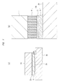
- FIG. 1 (a) is a cross-sectional view of a semiconductor device according to a first embodiment of the present invention
- FIG. 1(b) is an enlarged cross-sectional view showing a portion (region surrounded by a rectangular frame) of FIG. 1(a) .
- the semiconductor device of the first embodiment has a packaging structure in which an upper surface of a semiconductor chip 1 with a p-n junction formed therein is electrically connected to a conductive member 3a via a bonding member 2a and a lower surface is electrically connected to a conductive member 3b via a bonding member 2b. That is, a current flowing in from one of the pair of conductive members 3a and 3b is rectified by a diode element in the semiconductor chip 1, and flows out from the other of the conductive members 3a and 3b, whereby the semiconductor device functions as a diode.
- the semiconductor chip 1 is formed of single-crystal silicon (Si) provided with a diode function in a semiconductor manufacturing process (front-end process), and has dimensions such that each side is about 6 mm and a thickness is about 0.2 mm. Moreover, each of the pair of conductive members 3a and 3b constituting electrodes of the diode is formed of a metal plate such as copper (Cu).
- the bonding member 2b of the pair of bonding members 2a and 2b interposing the semiconductor chip 1 therebetween has a three-layer structure of a nanospring layer 4, a planar layer 5, and a bonding layer 6 in the order from the side close to the semiconductor chip 1.
- the bonding member 2a also has a three-layer structure of a nanospring layer 4, a planar layer 5, and a bonding layer 6 in the order from the side close to the semiconductor chip 1.
- An under layer 22 (described later) formed of a nickel film intervenes between the respective nanospring layers 4 of the bonding members 2a and 2b and the semiconductor chip 1, but the film thickness of the under layer 22 is extremely small, therefore, the under layer is not shown in FIG. 1 .
- the nanospring layer 4 connecting the semiconductor chip 1 with the planar layer 5 has a structure in which a plurality of coil-shaped springs having a nano-order size, that is, a size of equal to or less than 1 ⁇ m are disposed in a matrix.
- each of the plurality of coil-shaped springs has a substantially circular cross-sectional shape having a diameter of about 25 nm, and has an outside diameter of about 150 nm, an inside diameter of about 100 nm, and a height of about 10 ⁇ m.
- a distance between adjacent springs is about 50 nm, and the material of the spring is nickel (Ni).
- the bonding members 2a and 2b can efficiently absorb with the nanospring layer 4 a difference in thermal deformation between the semiconductor chip 1 and the conductive members 3a and 3b occurring at the time of operation.
- an increase in thermal stress can be prevented, and the cracking of the semiconductor chip 1 or the breakage of the bonding members 2a and 2b due to a thermal stress can be prevented.
- a difference in the linear coefficient of expansion between silicon as a main material of the semiconductor chip 1 and copper as a main material of the conductive members 3a and 3b is about 13 ppm/degree.
- a thermal deformation difference at the edge of the semiconductor chip 1 is about 8 ⁇ m.
- the nanospring layer 4 For absorbing the thermal deformation difference with the deformation of the nanospring layer 4, it is desirable for the nanospring layer 4 to have a thickness of at least 8 ⁇ m or more. In the first embodiment, therefore, the thickness of the nanospring layer 4 is set to 10 ⁇ m.
- the semiconductor chip 1 and the planar layer 5 are connected via a plurality of springs configured from nickel (Ni) having high thermal conductivity, a thermal resistance between the semiconductor chip 1 and the planar layer 5 can be reduced, and the heat generated in the semiconductor chip 1 at the time of operation can be efficiently transferred to the conductive members 3a and 3b to reduce the temperature rise of the semiconductor chip 1.
- Ni nickel
- the nanospring layer 4 it is possible to provide a highly reliable semiconductor device in which a thermal stress or temperature rise is reduced.
- the planar layer 5, which is a support member for preventing the plurality of springs of nano-order size that constitute the nanospring layer 4 from coming apart, is configured from, for example, a conductive material such as nickel and has a thickness of about 0.5 ⁇ m. Moreover, by disposing the planar layer 5 adjacent to the nanospring layer 4, a place to be bonded with the bonding layer 6 can be flat. Therefore, the bonding is facilitated, and at the same time, it is possible to prevent the bonding layer 6 from flowing into gaps of the nanospring layer 4 at the time of bonding. Further, when nickel is used for the material of the planar layer 5, the surface of the planar layer 5 is hardly oxidized at a manufacturing stage, therefore, it is possible to prevent a surface oxide layer from being obstructive to manufacture.
- the thickness of the planar layer 5 is about 0.5 ⁇ m, which is small compared to the nanospring layer 4.
- the reason for this is that by providing the planar layer 5 with reduced thickness, the bending stiffness of the planar layer 5 is reduced to improve the bondability when bonding the planar layer 5 and the conductive members 3a and 3b via the bonding layer 6. That is, even when there are irregularities on the surface of the planar layer 5 or the conductive members 3a and 3b before bonding, the irregularities are absorbed by the deformation of the nanospring layer 4, and favorable bonding can be obtained.
- the planar layer 5 since the planar layer 5 is thin and has a small bending stiffness, the planar layer 5 can follow the deformation of the nanospring layer 4. Further, since the planar layer 5 is thin, the thermal resistance of the planar layer 5 itself is reduced, so that the planar layer 5 can contribute to a reduction in the thermal resistance of the entire semiconductor device.
- the bonding layer 6 is formed of a solder material such as tin (Sn) or a tin alloy, and has a thickness of about 5 ⁇ m.
- a portion of the bonding members 2a and 2b does not include the nanospring layer 4
- a difference in thermal deformation between the semiconductor chip 1 and the conductive member 3 is absorbed by the deformation of the bonding layer 6, therefore, it is necessary to ensure a sufficient thickness of the bonding layer 6.
- a portion of the bonding members 2a and 2b includes the nanospring layer 4
- a difference in thermal deformation between the semiconductor chip 1 and the conductive member 3 can be absorbed by the deformation of the nanospring layer 4.
- the thickness of the bonding layer 6 can be sufficiently small.
- the bonding layer 6 can be thinned to a thickness of the order of ⁇ m or less.
- the thickness of the bonding layer 6, although larger than the planar layer 5, can be made smaller than the nanospring layer 4. Based on these facts, the bonding layer 6 is sufficiently thinned to reduce the thermal resistance thereof, so that the bonding layer 6 can contribute to a reduction in the thermal resistance of the entire semiconductor device.
- nickel is used for the material of the nanospring layer 4 or the planar layer 5
- other conductive materials such as copper can also be used.
- copper is used for the material of the nanospring layer 4 or the planar layer 5
- the thermal conductivity of the bonding members 2a and 2b is further improved, therefore, the thermal resistance of the entire semiconductor device can be further reduced.
- copper has a smaller modulus of elasticity or yield stress than that of nickel, the deformation absorbing effect of the nanospring layer 4 or the deformation following capability of the planar layer 5 is further improved.
- copper is an easily oxidizable material compared to nickel, oxidation prevention treatment may be required.
- a metal containing tin as a main component is used for the material of the bonding layer 6, a metal containing zinc (Zn) or silver (Ag) as a main component can also be used.
- Zn zinc
- Ag silver
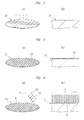
- FIG. 2 to FIG. 6 (a) is an overall perspective view of a semiconductor wafer, and (b) is an enlarged cross-sectional view of a surface edge of the semiconductor wafer.
- a semiconductor wafer 21 configured from a plurality of semiconductor chips 1 is prepared.
- a diode element formed of a p-n junction is formed.
- the under layer 22 formed of a nickel film is formed on the surface of the semiconductor wafer 21 using a vapor deposition method.
- the under layer 22 is provided for purposes of improving the bonding strength between the semiconductor chip 1 and the nanospring layer 4, or uniformly transferring electricity or heat to the nanospring layer 4.
- the under layer 22 can be formed by a plating method instead of a vapor deposition method.
- the metal layer can be used as the under layer 22, therefore, the step of forming the under layer 22 can be omitted.
- the semiconductor wafer 21 is rotated about an axis vertical to the surface of the under layer 22 under a substantially vacuum environment. Then, in this state, nickel atoms 23 are emitted from an evaporation source (not shown) disposed in the obliquely upward direction, and are vapor deposited on the surface of the under layer 22.
- nickel atoms 24 are vapor deposited from above the nanospring layer 4 to thereby form the planar layer 5 on the top of the nanospring layer 4 as shown in FIG. 5 .
- tin atoms 25 are vapor deposited from above the planar layer 5, with the rotation of the semiconductor wafer 21 stopped, to thereby form a bonding layer 26 before bonding on the top of the planar layer 5.
- the under layer 22, the nanospring layer 4, the planar layer 5, and the bonding layer 26 are formed in this order on the surface of the semiconductor wafer 21.
- a set of these layers is referred to as a surface forming layer 27.
- the same procedure as described above is carried out, whereby the surface forming layer 27 is also formed on the back surface of the semiconductor wafer 21 as shown in FIG. 7 .
- the surface forming layer 27 is formed on the both surfaces thereof.
- the surface forming layer 27 may be formed on the both surfaces of the semiconductor chip 1 by the method described above after dicing and singulating the semiconductor wafer 21.
- the nanospring layer 4 is formed by depositing the nickel atoms 23 from an oblique direction, consideration must be given so that the nickel atoms 23 are not vapor deposited on the side surface of the semiconductor chip 1.
- the semiconductor chip 1 with the surface forming layers 27 formed on the both surfaces is interposed between the pair of conductive members 3a and 3b, and further, a weight 42 used for pressurization at the time of bonding is disposed on the top of the conductive member 3a.
- the members are aligned using bonding jigs 41a and 41b made of carbon.
- the bonding layer 26 before bonding is formed on the both surfaces of the semiconductor chip 1, it is not necessary to separately stack a bonding material when aligning the members using the bonding jigs 41a and 41b, thereby making it possible to improve assemblability.
- the members aligned using the bonding jigs 41a and 41b are exposed to an environment of a melting point or higher of the bonding layer 26 before bonding, and thereafter, the temperature is lowered.
- the bonding layer 26 before bonding which is liquefied, reacts with the atoms constituting the planar layer 5 or the atoms constituting the conductive members 3a and 3b to be alloyed, and becomes the alloyed bonding layer 6 after lowering the temperature.
- the planar layer 5 and the conductive member 3a are bonded together, and the planar layer 5 and the conductive member 3b are bonded together.
- the alloyed bonding layer 6 is an alloy of tin and nickel, tin and copper, or tin, nickel, and copper.
- This bonding step is carried out using a reflow furnace under a substantially vacuum environment. Due to this, it is possible to reduce an unbonded portion or voids occurring at the time of bonding.
- the bonding jigs 41a and 41b and the weight 42, which are cooled down, are removed, whereby the semiconductor device of the first embodiment shown in FIG. 1 is completed.
- the nanospring layer 4 in which springs having dimensions of nano-order size, that is, less than 1 ⁇ m are densely disposed can be manufactured, it is possible to realize a semiconductor packaging structure having remarkable differences in structure and effect from the related art.
- FIG. 10(a) shows a microspring 10 having dimensions of micro-order size as a related art
- FIG. 10(b) shows a nanospring 11 obtained by simply scaling down the microspring 10 shown in FIG. 10(a) to a nano-order size
- FIG. 10(c) shows the nanospring layer 4 of the first embodiment in which the nanosprings 11 are densely disposed.
- the height of the needles and the thickness of the nanospring layer 4 are all set to the same value L.
- a maximum stress ( ⁇ max ) occurring in the needle is expressed by the following formula.
- ⁇ max 3 4 ⁇ Edu L 2 (wherein, E is the modulus of longitudinal elasticity, d is the wire diameter, and u is the shear displacement to be applied.)
- the stresses occurring in the nanospring layer 4 and the spring 11 of nano-order size are the same, while a stress 1000 times that of the nanospring layer 4 and the spring 11 occurs in the spring 10 of micro-order size where d is 1000 times that of the nanospring layer 4 and the spring 11, so that the prevention of breakage of the spring is a problem.
- a thermal resistance (R) is expressed by the following formula.
- R 4 ⁇ L ⁇ d 2 ⁇ n (wherein, ⁇ is the thermal conductivity of a material, and n is the number)
- the thermal resistances of the nanospring layer 4 and the spring 10 of micro-order size are the same, while the thermal resistance is 1000000 times that of the nanospring layer 4 and the spring 10 in the spring 11 of nano-order size, which makes the temperature rise of the semiconductor chip 1 remarkable.
- the height L needs to be increased by 32 times, and in this case, the thermal resistance is increased by 32 times.
- a function of achieving both deformation absorption and a low thermal resistance that are required of a semiconductor packaging structure is a function that cannot be realized by the spring 10 of micro-order size as a related art or the spring 11 of nano-order size obtained by simply scaling down the spring 10, but can be first realized by the nanospring layer 4 of the first embodiment.
- the packaging structure of the semiconductor chip 1 having diode characteristics has been described.
- the design of the packaging structure of the first embodiment may be appropriately changed according to conditions of each semiconductor chip.
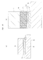
- FIG. 11(a) is a cross-sectional view of a semiconductor device according to a second embodiment of the present invention
- FIG. 11 (b) is an enlarged cross-sectional view showing a portion of FIG. 11(a) .
- springs constituting the nanospring layer 4 are not coil-shaped springs but are zigzag-shaped springs.
- the nanospring layer 4 is configured from zigzag-shaped springs, the occupied area per spring is reduced compared to coil-shaped springs, so that more springs can be disposed in a unit area. Moreover, the length of each spring when being straightened can be shortened.
- the thermal resistance of the nanospring layer 4 can be further reduced, but the efficiency of thermal deformation absorption may be lower than that of the coil-shaped spring.
- the shape of the spring may be selected in view of these features.
- FIG. 12 to FIG. 14 (a) is an overall perspective view of a semiconductor wafer, and (b) is an enlarged view of a surface edge of the semiconductor wafer.
- the under layer 22 is formed on the surface of the semiconductor wafer 21 by the same method as the first embodiment, and thereafter, as shown in Fig. 12 , the nickel atoms 23 are emitted from the obliquely upward direction of the semiconductor wafer 21 under a substantially vacuum environment, and are vapor deposited on the surface of the under layer 22. At this time, unlike the manufacturing method of the first embodiment, the semiconductor wafer 21 is not rotated.
- the semiconductor wafer 21 is rotated by 180 degrees about an axis vertical to the surface of the under layer 22. Due to this, the direction of the numerous columnar bodies that are vapor deposited and formed on the surface of the under layer 22 is opposite to the direction shown in FIG. 12 .
- FIG. 15(a) is a cross-sectional view of a semiconductor device according to a third embodiment of the present invention
- FIG. 15(b) is an enlarged cross-sectional view showing a portion of FIG. 15(a) .
- FIG. 15 shows an example in which two stages of the nanospring layers 4 are stacked.
- the springs constituting the nanospring layer 4 are not limited to the coil-shaped springs, and may be the zigzag-shaped springs as in the second embodiment.
- the nanospring layers 4 of the third embodiment are stacked in n stages, the amount of deformation to be absorbed by each of the nanospring layers 4 is reduced to 1/n, therefore, greater deformation can be absorbed.
- the thermal resistance or electrical resistance of the entire nanospring layers 4 is increased by n times.
- FIG. 16(a) is a cross-sectional view of a semiconductor device according to a fourth embodiment of the present invention
- FIG. 16(b) is an enlarged cross-sectional view of a portion of FIG. 16(a) .
- a difference from the first embodiment is that gaps of a plurality of springs constituting the nanospring layer 4 are filled with a resin 30.
- the average stiffness of the entire nanospring layer 4 can be controlled according to the physical properties of the resin 30 for filling.
- the gaps are filled with a resin having a small modulus of elasticity, the average stiffness of the entire nanospring layer 4 is reduced, and a thermal stress occurring in the semiconductor chip 1 or the conductive members 3a and 3b can be reduced.
- the gaps are filled with a resin having a large modulus of elasticity, the average stiffness of the entire nanospring layer 4 is increased, and a thermal deformation difference to be absorbed by the nanospring layer 4 is reduced. Therefore, the thermal resistance can be reduced by further thinning the nanospring layer 4.
- the material of the resin 30 for filling may be selected in view of these effects.
- the filling of the resin 30 is performed after bonding the semiconductor chip 1 with the conductive member 3. By doing this, an effect of absorbing surface irregularities due to the nanospring layer 4 at the time of bonding is not prevented by the resin 30. Moreover, the resin 30 may fill the entire gaps of the plurality of springs or may fill a portion of the gaps of the plurality of springs.
- the invention can be applied to a semiconductor device having a packaging structure in which a semiconductor chip is electrically connected to a conductive member via a bonding member.
Landscapes
- Cooling Or The Like Of Semiconductors Or Solid State Devices (AREA)
- Engineering & Computer Science (AREA)
- Manufacturing & Machinery (AREA)
- Electrodes Of Semiconductors (AREA)
- Die Bonding (AREA)
- Internal Circuitry In Semiconductor Integrated Circuit Devices (AREA)
Applications Claiming Priority (1)
| Application Number | Priority Date | Filing Date | Title |
|---|---|---|---|
| PCT/JP2013/050196 WO2014109014A1 (fr) | 2013-01-09 | 2013-01-09 | Dispositif à semi-conducteurs et son procédé de fabrication |
Publications (2)
| Publication Number | Publication Date |
|---|---|
| EP2945189A1 true EP2945189A1 (fr) | 2015-11-18 |
| EP2945189A4 EP2945189A4 (fr) | 2016-11-16 |
Family
ID=51166685
Family Applications (1)
| Application Number | Title | Priority Date | Filing Date |
|---|---|---|---|
| EP13870456.4A Withdrawn EP2945189A4 (fr) | 2013-01-09 | 2013-01-09 | Dispositif à semi-conducteurs et son procédé de fabrication |
Country Status (6)
| Country | Link |
|---|---|
| US (1) | US20150333024A1 (fr) |
| EP (1) | EP2945189A4 (fr) |
| JP (1) | JPWO2014109014A1 (fr) |
| CN (1) | CN104903998A (fr) |
| TW (1) | TW201442172A (fr) |
| WO (1) | WO2014109014A1 (fr) |
Cited By (2)
| Publication number | Priority date | Publication date | Assignee | Title |
|---|---|---|---|---|
| WO2022012903A1 (fr) * | 2020-07-13 | 2022-01-20 | Nanowired Gmbh | Élément de connexion, procédé de fabrication d'un élément de connexion, ensemble comprenant un élément de connexion et deux pièces reliées par ce dernier ainsi que procédé de connexion de deux pièces reliées par un élément de connexion |
| WO2023030788A1 (fr) * | 2021-08-30 | 2023-03-09 | Robert Bosch Gmbh | Ensemble électronique ayant un composant semi-conducteur de puissance entre deux supports de circuit, et son procédé de production |
Families Citing this family (4)
| Publication number | Priority date | Publication date | Assignee | Title |
|---|---|---|---|---|
| JP6380932B2 (ja) * | 2014-10-21 | 2018-08-29 | 株式会社日立製作所 | ナノオーダ構造体の製造方法および製造装置 |
| WO2016075733A1 (fr) * | 2014-11-10 | 2016-05-19 | 株式会社日立製作所 | Dispositif de conversion thermoélectrique et son procédé de fabrication |
| CN106048543B (zh) * | 2016-06-02 | 2018-08-03 | 泉州市依科达半导体致冷科技有限公司 | 半导体晶片表面真空镀膜工艺 |
| KR101916588B1 (ko) | 2017-05-15 | 2018-11-07 | 고려대학교 산학협력단 | 금속 나노스프링 및 이의 제조방법 |
Family Cites Families (23)
| Publication number | Priority date | Publication date | Assignee | Title |
|---|---|---|---|---|
| US5866204A (en) * | 1996-07-23 | 1999-02-02 | The Governors Of The University Of Alberta | Method of depositing shadow sculpted thin films |
| CA2591651C (fr) * | 1996-07-23 | 2010-09-28 | Micralyne Inc. | Films minces a motifs |
| JP3788343B2 (ja) | 2001-12-18 | 2006-06-21 | 日本電気株式会社 | 半導体装置とその製造方法 |
| JP4167443B2 (ja) | 2002-01-30 | 2008-10-15 | 日本放送協会 | 固体撮像素子 |
| US6864571B2 (en) * | 2003-07-07 | 2005-03-08 | Gelcore Llc | Electronic devices and methods for making same using nanotube regions to assist in thermal heat-sinking |
| US20050126766A1 (en) * | 2003-09-16 | 2005-06-16 | Koila,Inc. | Nanostructure augmentation of surfaces for enhanced thermal transfer with improved contact |
| TW200629511A (en) * | 2004-11-04 | 2006-08-16 | Koninkl Philips Electronics Nv | Nanotube-based connection arrangement and approach |
| JP2006287091A (ja) | 2005-04-04 | 2006-10-19 | Matsushita Electric Ind Co Ltd | 半導体装置およびその製造方法 |
| CN1891780B (zh) * | 2005-07-01 | 2013-04-24 | 清华大学 | 热界面材料及其制备方法 |
| US20080259976A1 (en) * | 2005-11-30 | 2008-10-23 | The Governors Of The University Of Alberta | Organic Columnar Thin Films |
| JP2007165383A (ja) * | 2005-12-09 | 2007-06-28 | Ibiden Co Ltd | 部品実装用ピンを形成したプリント基板 |
| JP4744360B2 (ja) * | 2006-05-22 | 2011-08-10 | 富士通株式会社 | 半導体装置 |
| EP1906496B1 (fr) * | 2006-09-29 | 2010-01-06 | OSRAM Opto Semiconductors GmbH | Laser semi-conducteur et son procédé de fabrication |
| US20080227294A1 (en) * | 2007-03-12 | 2008-09-18 | Daewoong Suh | Method of making an interconnect structure |
| KR101487346B1 (ko) * | 2007-09-12 | 2015-01-28 | 스몰텍 에이비 | 인접 층들을 나노구조들과 연결하고 결합하는 방법 |
| JP5146256B2 (ja) * | 2008-03-18 | 2013-02-20 | 富士通株式会社 | シート状構造体及びその製造方法、並びに電子機器及びその製造方法 |
| JP2009253073A (ja) * | 2008-04-08 | 2009-10-29 | Fujitsu Ltd | 半導体装置及びその製造方法 |
| JP2010189690A (ja) * | 2009-02-17 | 2010-09-02 | Toshiba Corp | 微小構造物の製造方法、微小構造物集合体、微小構造物、改質器、マイクロプラズマ発生装置、ガス検知用センシングデバイス、アクチュエータ及び圧力センシングデバイス |
| US7759165B1 (en) * | 2009-03-01 | 2010-07-20 | Rajeev Bajaj | Nanospring |
| JP5431793B2 (ja) * | 2009-05-29 | 2014-03-05 | 新光電気工業株式会社 | 放熱部品、電子部品装置及び電子部品装置の製造方法 |
| US8405996B2 (en) * | 2009-06-30 | 2013-03-26 | General Electric Company | Article including thermal interface element and method of preparation |
| US8592995B2 (en) * | 2009-07-02 | 2013-11-26 | Taiwan Semiconductor Manufacturing Company, Ltd. | Method and structure for adhesion of intermetallic compound (IMC) on Cu pillar bump |
| JP5870113B2 (ja) * | 2011-10-31 | 2016-02-24 | 株式会社日立製作所 | 半導体装置 |
-
2013
- 2013-01-09 EP EP13870456.4A patent/EP2945189A4/fr not_active Withdrawn
- 2013-01-09 CN CN201380069778.1A patent/CN104903998A/zh active Pending
- 2013-01-09 JP JP2014556250A patent/JPWO2014109014A1/ja active Pending
- 2013-01-09 WO PCT/JP2013/050196 patent/WO2014109014A1/fr not_active Ceased
- 2013-01-09 US US14/759,972 patent/US20150333024A1/en not_active Abandoned
- 2013-12-04 TW TW102144412A patent/TW201442172A/zh not_active IP Right Cessation
Cited By (2)
| Publication number | Priority date | Publication date | Assignee | Title |
|---|---|---|---|---|
| WO2022012903A1 (fr) * | 2020-07-13 | 2022-01-20 | Nanowired Gmbh | Élément de connexion, procédé de fabrication d'un élément de connexion, ensemble comprenant un élément de connexion et deux pièces reliées par ce dernier ainsi que procédé de connexion de deux pièces reliées par un élément de connexion |
| WO2023030788A1 (fr) * | 2021-08-30 | 2023-03-09 | Robert Bosch Gmbh | Ensemble électronique ayant un composant semi-conducteur de puissance entre deux supports de circuit, et son procédé de production |
Also Published As
| Publication number | Publication date |
|---|---|
| EP2945189A4 (fr) | 2016-11-16 |
| WO2014109014A1 (fr) | 2014-07-17 |
| US20150333024A1 (en) | 2015-11-19 |
| JPWO2014109014A1 (ja) | 2017-01-19 |
| TW201442172A (zh) | 2014-11-01 |
| TWI562301B (fr) | 2016-12-11 |
| CN104903998A (zh) | 2015-09-09 |
Similar Documents
| Publication | Publication Date | Title |
|---|---|---|
| TWI480993B (zh) | Semiconductor device and method for manufacturing semiconductor device | |
| US9620471B2 (en) | Power semiconductor package with conductive clips | |
| EP2945189A1 (fr) | Dispositif à semi-conducteurs et son procédé de fabrication | |
| US8525333B2 (en) | Electronic device and manufacturing method therefor | |
| US10249604B2 (en) | Semiconductor device and method of manufacturing the same | |
| US10153230B2 (en) | Method of manufacturing a semiconductor device comprising a semiconductor chip mounted over a metal plate having an inclined surface | |
| TW200947656A (en) | Lead frame, electronic component with the same, and manufacturing method thereof | |
| KR102574011B1 (ko) | 반도체 소자의 실장 구조 및 반도체 소자와 기판의 조합 | |
| EP1748480B1 (fr) | Structure de connexion pour fixer une puce semi-conductrice à un substrat métallique, puce semi-conductrice et composant électronique ayant cette structure de connexion et méthodes de fabrication de cette structure de connexion | |
| EP2775511B1 (fr) | Dispositif semi-conducteur | |
| JP2016129254A (ja) | 半導体装置 | |
| US11538734B2 (en) | Power semiconductor package with highly reliable chip topside | |
| US10109776B2 (en) | Light emitting device having curved light emitting element | |
| JP4417974B2 (ja) | 積層型半導体装置の製造方法 | |
| JP5098902B2 (ja) | 電子部品 | |
| JP2010056228A (ja) | 半導体装置およびその製造方法 | |
| JP5407707B2 (ja) | 半導体発光素子及びその製造方法 | |
| JP7418178B2 (ja) | 半導体装置、及び、その製造方法 | |
| US7605475B2 (en) | Semiconductor device | |
| CN212907708U (zh) | 二极管的封装结构 | |
| JP3175315U (ja) | 金属箔配線による半導体装置 | |
| CN121793782A (zh) | 半导体封装结构及其封装方法 | |
| TWI250628B (en) | Leadframe, semiconductor package and method for manufacturing the same | |
| JP2011204954A (ja) | 半導体装置及びその製造方法 |
Legal Events
| Date | Code | Title | Description |
|---|---|---|---|
| PUAI | Public reference made under article 153(3) epc to a published international application that has entered the european phase |
Free format text: ORIGINAL CODE: 0009012 |
|
| 17P | Request for examination filed |
Effective date: 20150810 |
|
| AK | Designated contracting states |
Kind code of ref document: A1 Designated state(s): AL AT BE BG CH CY CZ DE DK EE ES FI FR GB GR HR HU IE IS IT LI LT LU LV MC MK MT NL NO PL PT RO RS SE SI SK SM TR |
|
| AX | Request for extension of the european patent |
Extension state: BA ME |
|
| RIN1 | Information on inventor provided before grant (corrected) |
Inventor name: TANIE, HISASHI Inventor name: IKEDA, OSAMU |
|
| DAX | Request for extension of the european patent (deleted) | ||
| RIC1 | Information provided on ipc code assigned before grant |
Ipc: H01L 21/60 20060101ALI20160704BHEP Ipc: H01L 23/488 20060101AFI20160704BHEP Ipc: H01L 23/367 20060101ALI20160704BHEP |
|
| RIN1 | Information on inventor provided before grant (corrected) |
Inventor name: IKEDA, OSAMU Inventor name: TANIE, HISASHI |
|
| A4 | Supplementary search report drawn up and despatched |
Effective date: 20161014 |
|
| RIC1 | Information provided on ipc code assigned before grant |
Ipc: H01L 21/60 20060101ALI20161010BHEP Ipc: H01L 23/488 20060101AFI20161010BHEP Ipc: H01L 23/367 20060101ALI20161010BHEP |
|
| STAA | Information on the status of an ep patent application or granted ep patent |
Free format text: STATUS: THE APPLICATION HAS BEEN WITHDRAWN |
|
| 18W | Application withdrawn |
Effective date: 20161219 |