EP2945286B1 - Agencement d'amplificateur et procédé d'amplification - Google Patents
Agencement d'amplificateur et procédé d'amplification Download PDFInfo
- Publication number
- EP2945286B1 EP2945286B1 EP14167868.0A EP14167868A EP2945286B1 EP 2945286 B1 EP2945286 B1 EP 2945286B1 EP 14167868 A EP14167868 A EP 14167868A EP 2945286 B1 EP2945286 B1 EP 2945286B1
- Authority
- EP
- European Patent Office
- Prior art keywords
- potential
- level
- connection node
- amplifier
- input
- Prior art date
- Legal status (The legal status is an assumption and is not a legal conclusion. Google has not performed a legal analysis and makes no representation as to the accuracy of the status listed.)
- Active
Links
Images


Classifications
-
- H—ELECTRICITY
- H03—ELECTRONIC CIRCUITRY
- H03F—AMPLIFIERS
- H03F1/00—Details of amplifiers with only discharge tubes, only semiconductor devices or only unspecified devices as amplifying elements
- H03F1/26—Modifications of amplifiers to reduce influence of noise generated by amplifying elements
-
- H—ELECTRICITY
- H03—ELECTRONIC CIRCUITRY
- H03F—AMPLIFIERS
- H03F1/00—Details of amplifiers with only discharge tubes, only semiconductor devices or only unspecified devices as amplifying elements
- H03F1/34—Negative-feedback-circuit arrangements with or without positive feedback
-
- H—ELECTRICITY
- H03—ELECTRONIC CIRCUITRY
- H03F—AMPLIFIERS
- H03F3/00—Amplifiers with only discharge tubes or only semiconductor devices as amplifying elements
- H03F3/181—Low-frequency amplifiers, e.g. audio preamplifiers
- H03F3/183—Low-frequency amplifiers, e.g. audio preamplifiers with semiconductor devices only
- H03F3/185—Low-frequency amplifiers, e.g. audio preamplifiers with semiconductor devices only with field-effect devices
-
- H—ELECTRICITY
- H03—ELECTRONIC CIRCUITRY
- H03F—AMPLIFIERS
- H03F3/00—Amplifiers with only discharge tubes or only semiconductor devices as amplifying elements
- H03F3/26—Push-pull amplifiers; Phase-splitters therefor
-
- H—ELECTRICITY
- H04—ELECTRIC COMMUNICATION TECHNIQUE
- H04R—LOUDSPEAKERS, MICROPHONES, GRAMOPHONE PICK-UPS OR LIKE ACOUSTIC ELECTROMECHANICAL TRANSDUCERS; ELECTRIC HEARING AIDS; PUBLIC ADDRESS SYSTEMS
- H04R19/00—Electrostatic transducers
- H04R19/005—Electrostatic transducers using semiconductor materials
-
- H—ELECTRICITY
- H04—ELECTRIC COMMUNICATION TECHNIQUE
- H04R—LOUDSPEAKERS, MICROPHONES, GRAMOPHONE PICK-UPS OR LIKE ACOUSTIC ELECTROMECHANICAL TRANSDUCERS; ELECTRIC HEARING AIDS; PUBLIC ADDRESS SYSTEMS
- H04R19/00—Electrostatic transducers
- H04R19/04—Microphones
-
- H—ELECTRICITY
- H03—ELECTRONIC CIRCUITRY
- H03F—AMPLIFIERS
- H03F2200/00—Indexing scheme relating to amplifiers
- H03F2200/03—Indexing scheme relating to amplifiers the amplifier being designed for audio applications
-
- H—ELECTRICITY
- H03—ELECTRONIC CIRCUITRY
- H03F—AMPLIFIERS
- H03F2200/00—Indexing scheme relating to amplifiers
- H03F2200/153—Feedback used to stabilise the amplifier
-
- H—ELECTRICITY
- H03—ELECTRONIC CIRCUITRY
- H03F—AMPLIFIERS
- H03F2200/00—Indexing scheme relating to amplifiers
- H03F2200/471—Indexing scheme relating to amplifiers the voltage being sensed
-
- H—ELECTRICITY
- H04—ELECTRIC COMMUNICATION TECHNIQUE
- H04R—LOUDSPEAKERS, MICROPHONES, GRAMOPHONE PICK-UPS OR LIKE ACOUSTIC ELECTROMECHANICAL TRANSDUCERS; ELECTRIC HEARING AIDS; PUBLIC ADDRESS SYSTEMS
- H04R2201/00—Details of transducers, loudspeakers or microphones covered by H04R1/00 but not provided for in any of its subgroups
- H04R2201/003—Mems transducers or their use
Definitions
- the present invention relates to an amplifier arrangement and to an amplification method to be performed with an amplifier arrangement.
- Amplifiers are widely used in electronic circuits. In various applications amplifier arrangements may be used for amplifying microphone signals, in particular from microelectromechanical systems, MEMS, microphones.
- super source follower stages may be used, which buffer an input voltage signal.
- an input transistor is connected between supply terminals by means of respective current sources.
- One terminal of the input transistor is connected to a further amplifier stage that compares the resulting signal to a reference voltage.
- a further terminal of the input transistor is connected to an output of the amplifier arrangement by a feedback path.
- Document US 2007/0103207 A1 discloses a similar source follower with an input transistor connected between supply terminals by means of respective current sources. A pair of complementary MOS transistors is used to minimize a voltage drop across the upper current source for increasing a voltage swing at the input transistor.
- An amplifier arrangement comprises an input transistor with a first terminal coupled to a first reference potential terminal by means of a current sink, with a second terminal coupled to a second reference potential terminal by means of a current source, and with a control terminal connected to a signal input.
- Such an amplifier arrangement further comprises an amplifier stage with an amplifier output coupled to a first connection node between the current sink and the first terminal of the input transistor by means of a feedback path, and with an amplifier input connected to a second connection node between the current source and the second terminal of the input transistor.
- the input transistor is a field effect transistor, its first terminal being a source connection and its second terminal being a drain connection. Consequently, the control terminal is a gate connection.
- the improved amplification concept is based on the idea that a potential at the second connection node is controlled depending on a voltage level at the signal input.
- a level-shifting structure is included in the improved amplification concept that comprises a level-shifting element with one end connected to a reference connection that follows the input signal.
- the level-shifting element is further applied such that it is adapted to perform a level-shifting of a potential at the second connection node with respect to a potential at the reference connection.
- the reference connection may be coupled to the amplifier output, to the first connection node or to the control terminal of the input transistor, which more or less all follow the voltage level of the input signal.
- the level-shifting at the second connection node has the effect that for small input signals the potential at the second connection node is low with respect to a supply potential at the second reference potential terminal. Hence, there is a higher voltage drop across the current source. Under such circumstances, a good noise performance of the amplifier arrangement can be achieved, in particular with respect to power supply rejection ratio, PSRR.
- PSRR power supply rejection ratio
- lower input voltages are defined as being low in relation to a supply voltage.
- higher input voltages are in the range of the supply voltage itself.
- a dynamic trade-off between a low noise operation at small input signals and a low distortion operation at large input signals is made.
- the potential at the second connection node between the current source and the second terminal of the input transistor also the voltage drop across the current source is controlled dynamically.
- a voltage difference between a first and a second terminal of the input transistor can be controlled to be basically always at or above a certain minimum level, which may be a saturation voltage plus some safety margin of, for example, 100 mV.
- an amplifier arrangement according to the improved concept comprises the level-shifting structure described above.
- an amplification method according to the improved concept is performed with an amplifier arrangement comprising the input transistor connected between the current source and the current sink, and the amplifier stage as described above.
- a level-shifting of a potential at the second connection node is performed with respect to a potential at the reference connection as described above.
- the level-shifting structure is adapted to limit the potential at the second connection node to a predefined voltage level below a potential at the second reference potential terminal.
- a voltage drop over the current source is present regardless of a voltage level of the input signal.
- This serves, for example, the purpose of avoiding unwanted conditions of the amplifier arrangement, during which both the first and the second connection node tend to a positive supply voltage. Under such conditions it may be possible that the arrangement becomes stuck in an unwanted state due to the feedback path.
- the limiting is not necessary for all cases, in particular not for cases where an input signal amplitude may be limited.
- the level-shifting structure comprises a further level-shifting element with one end connected to the first reference potential terminal.
- the further level-shifting element is adapted to perform a level-shifting of the potential at the second connection node with respect to a potential at the first reference potential terminal, which is preferably a fixed potential that does not float with the input signal.
- the level-shifting structure further comprises a comparison unit that is adapted to activate either of the level-shifting element and the further level-shifting element for performing the level-shifting at the second connection node. A decision on which one of the level-shifting element and the further level-shifting element is activated is based on an evaluation of the potential at the reference connection and/or the first connection node.
- a level-shifting based on a floating level or a level-shifting based on a fixed level can be performed. This can, for example, be used for delimiting of the potential at the second connection node as described above.
- the comparison unit is adapted to activate one of the level-shifting element and the further level-shifting element for performing the level-shifting at the second connection node depending on a comparison of the potential at the reference connection with a threshold voltage.
- the comparison unit is adapted to activate the level-shifting element for performing a level-shifting at the second connection node if the potential at the reference connection is lower than a threshold voltage, and to activate the further level-shifting element for performing the level-shifting at the second connection node if the potential at the reference connection is higher than the threshold voltage.
- the decision on which level-shifting element to activate is based on an evaluation of a potential at the floating reference connection, limiting the voltage at the second connection node.
- the comparison unit is adapted to activate the level-shifting element for performing a level-shifting at the second connection node if the potential at the reference connection is higher than a threshold voltage, and to activate the further level-shifting element for performing the level-shifting at the second connection node if the potential at the reference connection is lower than the threshold voltage.
- This implementation allows the amplifier stage to have an input stage which is not rail to rail type.
- the comparison unit is adapted to activate the level-shifting element for performing a level-shifting at the second connection node if a potential at the control terminal is higher than the potential at the first connection node, and to activate the further level-shifting element for performing the level-shifting at the second connection node if the potential at the control terminal is lower than the potential at the first connection node.
- the potential at the control terminal of the input transistor is evaluated with respect to a potential at the first connection node.
- level-shifters are activated while the other one is deactivated and does not actually perform level-shifting. Hence, it may be switched between the two level-shifters depending on the comparison result.
- the amplifier stage is implemented as a differential amplifier or an operational amplifier.
- the amplifier input may be an inverting input of the amplifier stage.
- the amplifier stage may then further comprises a non-inverting input.
- the level-shifting element has the one end connected to the reference connection and the second end coupled to the non-inverting input. Hence, there is a fixed level-shifting between the reference connection and the non-inverting input. If, for example, the reference connection is coupled to the first connection node, the level-shifting element determines a voltage between the first and the second terminal of the input transistor.
- the level-shifting element is at least partially formed of a further input transistor of the amplifier stage.
- a threshold voltage of one of the transistors of a transistor stage of the amplifier stage implements the level-shifting if, for example, the control terminal of said transistor is connected to the reference connection.
- the amplifier stage is implemented with a positive input offset such that an output potential at the amplifier output assumes a potential at the first reference potential terminal in case a voltage difference between the amplifier input and the further amplifier input is zero.
- a predefined output in particular with a low output potential, can be generated even in the case of the positive supply voltage being present at the amplifier input and the further amplifier input.
- a monitor circuit is foreseen that is configured to detect a condition where both a potential at the first connection node and the potential at the second connection node converge to a potential at the second reference potential terminal, and to reset the amplifier stage in response to such detection. Also with such implementations unwanted operating conditions can be avoided.
- the input transistor may be chosen as an n-channel field effect transistor.
- a p-channel field effect transistor can be used in alternative implementations, wherein the circuit is flipped in this case with respect to the polarity of the supply provided at the first and the second reference potential terminal.
- the improved amplification concept may advantageously used in conjunction with capacitive MEMS microphones providing the input voltage to be amplified.
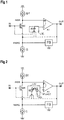
- Figure 1 shows an embodiment of an amplifier arrangement according to the improved amplification concept, which may be regarded as a basic implementation for the improved concept and the further embodiments described in conjunction with Figure 2 to Figure 8 .
- the amplifier arrangement comprises an input transistor MIN with a first terminal, which in this case is a source terminal, being coupled to a first reference potential terminal VSS by means of a current sink IS.
- a second terminal of the input transistor MIN which in this case is a drain terminal, is coupled to a second reference potential terminal VDD by means of a current source IB1.
- a control terminal of the input transistor which in this case is a gate terminal, is connected to a signal input IN.
- a first connection node INSRC is formed by the connection between the first terminal and the current sink IS.
- a second connection node INDR is formed by a connection of the second terminal and the current source IB1.
- the input transistor MIN in the embodiment of Figure 1 is chosen as an n-channel field effect transistor.
- a p-channel field effect transistor can be used in alternative implementations, wherein the circuit is flipped in this case with respect to the polarity of the supply provided at the first and the second reference potential terminal VSS, VDD. Such modifications become apparent for the skilled person.
- the amplifier arrangement further comprises an amplifier stage A1 with a first input coupled to the second connection node INDR.
- the first amplifier input may be a non-inverting input in this case.
- the amplifier stage A1 comprises an amplifier output OUT that is coupled to the first connection node INSRC by means of a feedback path FB.
- the amplifier arrangement further comprises a level-shifting structure LSC, which operates over a second amplifier input, in particular a non-inverting input, to the first amplifier input or to the second connection node INDR, respectively.
- the level-shifting structure LSC comprises a level-shifting element VS with one end connected to a reference connection that is coupled to one of three possible nodes.
- the reference connection is connected to the amplifier output OUT.
- the reference connection is coupled to the first connection node INSRC, and according to a third option, the reference connection is coupled to the control terminal of the input transistor MIN or the signal input IN, respectively.
- the dashed lines showing these connections express that only one of these optional connections is present in each case.
- the level-shifting element VS is adapted to perform a level-shifting of a potential at the second connection node INDR with respect to a potential at the reference connection. All of the three nodes, to which the reference connection can be coupled, have in common that their voltage level follows a level of an input signal provided at the signal input IN. Hence, the potential at the second connection node INDR is shifted by a certain amount with respect to a potentially changing voltage level at the reference connection.
- the implementation of the amplifier arrangement according to the improved amplification concept uses a source follower concept generally known in the art.
- the feedback path FB provides a feedback loop that may be used to set a certain gain or frequency response of the amplifier arrangement. Despite such amplification gain or frequency response, an output signal at the amplifier output OUT represents a buffered version of the input signal.
- a voltage at the second connection node INDR is controlled based on a voltage following a voltage level of an input signal.
- the employment of the level-shifting structure effects that the drain voltage of the input transistor MIN, i.e. the voltage at the second connection node INDR is controlled and therefore also the voltage drop across the current source IB1 is controlled dynamically.
- a voltage difference between drain and source of the input transistor MIN is always at or above a certain predefined minimum voltage.
- a predefined minimum voltage is defined as a saturation voltage of the transistor plus a safety margin of, for example, 100 mV.
- the level-shifting structure LSC represents a mechanism which makes the second connection node INDR dynamically trace the voltage on the first connectin node INSRC or any of its following nets such as the signal input node IN, with a monotonically increasing behavior, which is not necessarily linear.
- the drain-to-source voltage of the input transistor MIN can be biased with very small headroom during the normal operation, and all the voltage headroom can be used for the current source IB1 to enhance the PSRR and noise performance.
- the level-shifting element VS may be a voltage source, whose voltage may be chosen arbitrarily, as long as a reasonable DC biasing for the amplifier can be established.
- the current source IB1 and the current sink IS may be implemented as a controlled field effect transistor or a defined resistor or other implementations of current sources or current sinks known in the art.
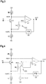
- Figure 2 shows a further embodiment of an amplifier arrangement according to the improved amplification concept.
- Figure 2 shows a development of the embodiment of Figure 1 .
- the differences to the previous embodiment will be mainly described in the following.
- the level-shifting structure LSC further to the level-shifting element VS, comprises a further level-shifting element VCONST that is connected to the first reference potential terminal VSS with one end.
- a switching element or multiplexer is included in the level-shifting structure LSC which is adapted to connect either the level-shifting element VS or the further level-shifting element VCONST such that the level-shifting of the potential at the second connection node INDR can be performed.
- the switching preferably is controlled by a comparison unit (not shown) that evaluates the potential at the reference connection or a potential derived from said potential.
- the comparison unit compares a potential resulting from the potential at the reference connection plus the level-shifting contributed by the level-shifting element VS with the potential generated by the further level-shifting element VCONST.
- the potentials at the upper ends of the level-shifters VS, VCONST, both connected to the switch may be compared.
- the larger potential of the two is used for the actual level-shifting such that only one of the level-shifting elements VS, VCONST is activated while the other one is deactivated.
- the voltage at the second connection node INDR is set either to a voltage which is a certain level, defined by the level-shifting element VS, above the reference connection potential, or to a constant voltage defined by the further level-shifting element VCONST, whichever is higher.
- the amplifier stage A1 allows, for example, the amplifier stage A1 to be of a non-rail-to-rail type.
- the implementation of Figure 2 can also be used to limit the potential at the connection node INDR.
- the further level-shifting element VCONST generates a voltage level which is a predefined voltage level below a potential at the second reference potential terminal VDD.
- the comparison described before is performed such that not the larger resulting voltage level, but the smaller resulting voltage level, is used for the level-shifting.
- the potential at the second connection node INDR follows the potential at the reference connection.
- a safety margin is kept such that the voltage drop across the current source IB1 does not become zero.
- FIG 3 shows a further implementation of the improved amplification concept, which is based on the embodiment of Figure 1 .
- the level-shifting element VS is connected to the first connection node INSRC at its first end.
- the first connection node INSRC is the reference connection in the specific implementation, which of course can be altered as described for Figure 1 .
- the second end of the level-shifting element VS is connected to the second amplifier input.
- the voltage drop across the input transistor MIN is controlled to be equal to the level-shifting voltage of the level-shifting element VS.
- Figure 4 shows a further example implementation according to the improved amplification concept that is based on the embodiments described in the previous figures, in particular with respect to Figure 2 .
- the level-shifting element VS has its one end connected to the first connection node INSRC.
- the second end of the level-shifting element VS is connected to an input A of a control block, while a further input B of the control block is connected to the further level-shifting element VCONST.
- An output Y of the block is connected to the second input of the amplifier stage A1.
- the control block compares the voltage levels at the inputs A, B and provides one of the input voltages to its output Y or the second amplifier input, respectively.
- the control block may include the above-mentioned comparison unit and respective switches or a multiplexer. It may be expedient if an input voltage is limited not to exceed or even be close to the positive supply voltage at VDD in order to have the amplifier arrangement according to the improved amplification concept in a safe and controlled operating state.
- a maximum voltage which is generated by the level-shifting element VS or that is present at the second connection node INDR can be limited to a voltage smaller than the positive supply voltage at VDD.
- a further approach is to implement a DC voltage feedback in the feedback path FB which ensures that the first connection node INSRC, or in general the reference connection, is always at least the voltage level of the level-shifting element VS plus some safety margin below the positive supply voltage at VDD.
- a monitor circuit can be provided that detects the undesired operating state and resets the amplifier upon detection.
- a circuit is implemented which monitors the operation point of the input transistor MIN and resets the amplifier if the input transistor MIN gets out of its normal operation point.
- the operation point of the circuit is monitored by a comparator CMP1 which compares the gate voltage of the input transistor MIN with the potential at the first connection node INSRC and controls a switching between the level-shifting element VS and the further level-shifting element VCONST by means of a multiplexer switch MUX1. If the source voltage of the input transistor MIN approaches the gate potential this means that the input transistor MIN leaves the normal conducting operation range. In this case, the comparator CMP1 connects the second input of the amplifier stage A1 to the fixed level-shifting element VCONST having a potential that is sufficiently below the positive supply voltage at VDD. The regulation loop then avoids the unwanted operating state.
- the feedback path FB comprises resistors R1, R2 and a capacitor C1 for setting a gain and frequency response of the feedback loop.
- resistors R1, R2 and a capacitor C1 for setting a gain and frequency response of the feedback loop.
- Such implementation can also be used with the other embodiments.
- Figure 6 shows a further implementation that is based on the embodiment of Figure 1 and is further similar to the embodiment of Figure 5 .
- the amplifier stage A1 is implemented as a high gain stage with a folded cascade stage MC together with a class AB output stage with transistors Mop and Mon.
- the input signal tracing mechanism is realized by biasing the folded cascade transistor MC with the source node of MIN or the first connection node INSRC, respectively.
- the drain-to-source headroom of the input transistor MIN is therefore defined by the threshold voltage of the transistor MC.
- the level-shifting element VS is implemented with the transistor MC in this implementation.
- the potentials at the input node IN and the output node OUT, namely through the direct feedback FB, are compared to check if there is any current flowing through the input transistor MIN.
- the result of the comparison performed by the comparator CMP1 is used to control the multiplexer MUX1, in order to define the DC operating point for ensuring a safe operation of the circuit.
- Figure 7 shows a further example of an amplifier arrangement according to the improved amplification concept based on the previously described embodiments, at least the embodiment of Figure 1 .
- the amplification stage A1 in Figure 7 is implemented with a differential amplifier comprising transistors M1, M2, M3, M4 together with a class AB output stage with transistors Mop, Mon.
- the level-shifting element is implemented with the transistor MIS, whose threshold voltage acts as a level-shifter connecting the first connection node INSRC as the reference connection to the second amplifier input at transistor M2 via the multiplexer MUX1.
- the first amplifier input is at the transistor M1.
- the transistor MIS, together with the current source IB3 connecting the transistor MIS to the second reference potential terminal VDD implements a source follower stage and realizes a floating voltage source for providing the level-shifting.
- the comparator CMP1 and the multiplexer MUX1 evaluate the voltage level at the reference connection or the first connection node INSRC by a comparison with a threshold voltage VB1.
- a threshold voltage VB1 For a large signal input, the voltage level on the second connection node INDR or the drain node of the input transistor MIN has a bottom limit set by a voltage provided by the level-shifting element VB2, therefore a minimum voltage headroom for the input transistor MIN is guaranteed.
- Figure 8 shows a further implementation of an amplifier arrangement according to the improved amplification concept, which has a capacitive MEMS microphone connected at the input IN.
- the MEMS microphone is biased by a voltage source VBIASMEMS.
- the transistor MS represents the level-shifting element VS for performing a level-shifting with respect to the first connection node INSRC as the reference connection.
- the inputs of the amplifier stage A1 are realized as the gate and source connections of the transistor MC, whose drain terminal is connected to an amplifying element.
- the output of the amplifying element is connected to a class AB output stage with transistors Mop, Mon, as previously described.
- the comparator CMP1 compares the voltage at the input terminal IN with the voltage at the reference connection, which here is the first connection node INSRC.
- the comparator CMP1 controls the multiplexer MUX1 for either providing the voltage of the transistor MS or of the voltage source VB1 to the gate of the transistor MC.
- the transistor MC is always biased in triode region, such that the transistor MC behaves like a voltage-controlled resistor.
- the output resistance value of the transistor MC is small enough, so the drain node of the input transistor MIN, respectively the second connection node INDR, is biased at the voltage of the voltage source VB2. Therefore, more freedom can be obtained to define the drain source voltage of the input transistor MIN to save headroom, for example compared to the embodiment of Figure 6 .
- the resistance value of the transistor MC increases. That means that also the drain source voltage of the transistor MC increases.
- the current source IB1 pulls up the drain node of the input transistor MIN, in particular higher than the voltage of voltage source VB2. Therefore, the operation range of the input transistor MIN is extended.
- the current mode level shifter comprises the current source IB2, the current sink IS2 and the transistor MS, which can also be added to the circuit shown in Figure 6 in order to bias the cascade transistor MC, which is not working in the triode region but in the saturation region.
- the amplifier connecting the transistor MC to the class AB output stage can be omitted such that the drain node of the cascade transistor MC is directly connected to the input of the class AB stage. Therefore, the drain source headroom of the input transistor MIN is defined by the threshold difference of the transistors MS and MC, and more freedom for choosing the drain source bias voltage for the input transistor MIN can be achieved.
- both a good noise performance in particular a good PSRR and a low total harmonic distortion, THD
- the clipping point inside the amplifier arrangement can be removed.
- a significant voltage headroom saving for the amplifier can be provided to achieve operations with large input signals, while maintaining good noise, PSRR and THD performance for small input signals.
- the input characteristic is not affected either.
- the improved amplification concept is suitable for low noise rail-to-rail input and output applications with a high dynamic range.
- the improved amplification concept can be well used with microphone applications, in particular with MEMS microphones.
- class AB stage used in various embodiments described above, is only used as an example. Other kinds of output stages may also be used.
Landscapes
- Engineering & Computer Science (AREA)
- Power Engineering (AREA)
- Physics & Mathematics (AREA)
- Acoustics & Sound (AREA)
- Signal Processing (AREA)
- Multimedia (AREA)
- Amplifiers (AREA)
Claims (15)
- Agencement d'amplificateur comprenant- un transistor d'entrée (MIN) présentant une première borne couplée à une première borne de potentiel de référence (VSS) moyennant un puits de courant (IS), une deuxième borne couplée à une deuxième borne de potentiel de référence (VDD) moyennant une source de courant (IB1), et une borne de commande connectée à une entrée de signal (IN);- un étage d'amplificateur (A1) présentant une sortie d'amplificateur (OUT) couplée à un premier noeud de connexion (INSRC) entre le puits de courant (IS) et la première borne du transistor d'entrée (MIN) moyennant un chemin de rétroaction (FB), et une entrée d'amplificateur connectée à un deuxième noeud de connexion (INDR) entre la source de courant (IB1) et la deuxième borne du transistor d'entrée (MIN); et- une structure de décalage de niveau (LSC) comprenant un élément de décalage de niveau (VS) dont une extrémité est connectée à une connexion de référence qui est couplée à l'un des éléments suivants: la sortie d'amplificateur (OUT), le premier noeud de connexion (INSRC), la borne de commande du transistor d'entrée (MIN);- sachant que l'élément de décalage de niveau (VS) est apte à commander un potentiel au niveau du deuxième noeud de connexion (INDR) pour suivre un niveau d'un signal d'entrée fourni au niveau de l'entrée de signal (IN) en effectuant un décalage de niveau du potentiel au niveau du deuxième noeud de connexion (INDR) par rapport à un potentiel au niveau de la connexion de référence, le décalage de niveau étant effectué via une entrée d'amplificateur supplémentaire de l'étage d'amplificateur (A1) .
- Agencement d'amplificateur selon la revendication 1, sachant que la structure de décalage de niveau (LSC) est apte à limiter le potentiel au niveau du deuxième noeud de connexion (INDR) à un niveau de tension prédéfini sous un potentiel au niveau de la deuxième borne de potentiel de référence (VDD).
- Agencement d'amplificateur selon la revendication 1 ou 2, sachant que la structure de décalage de niveau (LSC) comprend- un élément de décalage de niveau supplémentaire (VCONST) dont une extrémité est connectée à la première borne de potentiel de référence (VSS), l'élément de décalage de niveau supplémentaire (VCONST) étant apte à effectuer un décalage de niveau du potentiel au niveau du deuxième noeud de connexion (INDR) par rapport à un potentiel au niveau de la première borne de potentiel de référence (VSS); et- une unité de comparaison qui est apte à activer l'un ou l'autre de l'élément de décalage de niveau (VS) et de l'élément de décalage de niveau supplémentaire (VCONST) pour effectuer le décalage de niveau au niveau du deuxième noeud de connexion (INDR) sur la base d'une évaluation du potentiel au niveau de la connexion de référence et/ou du premier noeud de connexion (INSRC).
- Agencement d'amplificateur selon la revendication 3, sachant que l'unité de comparaison est apte à activer l'un de l'élément de décalage de niveau (VS) et de l'élément de décalage de niveau supplémentaire (VCONST) pour effectuer le décalage de niveau au niveau du deuxième noeud de connexion (INDR) en fonction d'une comparaison du potentiel au niveau de la connexion de référence avec une tension seuil.
- Agencement d'amplificateur selon la revendication 3, sachant que l'unité de comparaison est apte à activer l'élément de décalage de niveau (VS) pour effectuer le décalage de niveau au niveau du deuxième noeud de connexion (INDR) si un potentiel au niveau de la borne de commande est supérieur au potentiel au niveau du premier noeud de connexion (INSRC), et à activer l'élément de décalage de niveau supplémentaire (VCONST) pour effectuer le décalage de niveau au niveau du deuxième noeud de connexion (INDR) si le potentiel au niveau de la borne de commande est inférieur au potentiel au niveau du premier noeud de connexion (INSRC).
- Agencement d'amplificateur selon l'une des revendications 1 à 5, sachant que- l'entrée d'amplificateur est une entrée inverseuse de l'étage d'amplificateur (A1);- l'entrée d'amplificateur supplémentaire comprend une entrée non inverseuse; et- l'élément de décalage de niveau (VS) a l'une extrémité qui est connectée à la connexion de référence et une deuxième extrémité qui est couplée à l'entrée non inverseuse.
- Agencement d'amplificateur selon l'une des revendications 1 à 5, sachant que l'élément de décalage de niveau (VS) est au moins en partie composé d'un transistor d'entrée supplémentaire de l'étage d'amplificateur (A1).
- Agencement d'amplificateur selon l'une des revendications 1 à 7, sachant que l'étage d'amplificateur (A1) est implémenté avec un écart d'entrée positif de telle sorte qu'un potentiel de sortie au niveau de la sortie d'amplificateur (OUT) présente un potentiel au niveau de la première borne de potentiel de référence (VSS) dans le cas où une différence de tension entre l'entrée d'amplificateur et une entrée d'amplificateur supplémentaire est de zéro.
- Agencement d'amplificateur selon l'une des revendications 1 à 8, comprenant en outre un circuit de surveillance () qui est configuré pour détecter un état où à la fois un potentiel au niveau du premier noeud de connexion (INSRC) et le potentiel au niveau du deuxième noeud de connexion (INDR) convergent en un potentiel au niveau de la deuxième borne de potentiel de référence (VDD), et pour réinitialiser l'étage d'amplificateur (A1) en réponse à une telle détection.
- Procédé d'amplification destiné à être exécuté avec un agencement d'amplificateur comprenant- un transistor d'entrée (MIN) présentant une première borne couplée à une première borne de potentiel de référence (VSS) moyennant un puits de courant (IS), une deuxième borne couplée à une deuxième borne de potentiel de référence (VDD) moyennant une source de courant (IB1), et une borne de commande connectée à une entrée de signal (IN); et- un étage d'amplificateur (A1) présentant une sortie d'amplificateur (OUT) couplée à un premier noeud de connexion (INSRC) entre le puits de courant (IS) et la première borne du transistor d'entrée (MIN) moyennant un chemin de rétroaction (FB), et une entrée d'amplificateur connectée à un deuxième noeud de connexion (INDR) entre la source de courant (IB1) et la deuxième borne du transistor d'entrée (MIN);le procédé comprenant:- la commande d'un potentiel au niveau du deuxième noeud de connexion (INDR) pour suivre un niveau d'un signal d'entrée fourni au niveau de l'entrée de signal (IN) en effectuant un décalage de niveau d'un potentiel au niveau du deuxième noeud de connexion (INDR) par rapport à un potentiel au niveau d'une connexion de référence qui est couplée à l'un des éléments suivants: la sortie d'amplificateur (OUT), le premier noeud de connexion (INSRC), la borne de commande du transistor d'entrée (MIN);- sachant que le décalage de niveau est effectué via une entrée d'amplificateur supplémentaire de l'étage d'amplificateur (A1).
- Procédé selon la revendication 10, comprenant en outre la limitation du potentiel au niveau du deuxième noeud de connexion (INDR) à un niveau de tension prédéfini sous un potentiel au niveau de la deuxième borne de potentiel de référence (VDD).
- Procédé selon la revendication 10 ou 11, comprenant en outre le fait d'effectuer un décalage de niveau du potentiel au niveau du deuxième noeud de connexion (INDR) par rapport à sélectivement l'un ou l'autre du potentiel au niveau de la connexion de référence ou d'un potentiel au niveau de la première borne de potentiel de référence (VSS), sur la base d'une évaluation du potentiel au niveau de la connexion de référence et/ou du premier noeud de connexion (INSRC).
- Procédé selon la revendication 12,
sachant que le décalage de niveau est effectué par rapport au potentiel au niveau de la connexion de référence si le potentiel au niveau de la connexion de référence est inférieur à une tension seuil, et par rapport au potentiel au niveau de la première borne de potentiel de référence (VSS) si le potentiel au niveau de la connexion de référence est supérieur à la tension seuil. - Procédé selon la revendication 12,
sachant que le décalage de niveau est effectué par rapport au potentiel au niveau de la connexion de référence si un potentiel au niveau de la borne de commande est supérieur au potentiel au niveau du premier noeud de connexion (INSRC), et par rapport au potentiel au niveau de la première borne de potentiel de référence (VSS) si le potentiel au niveau de la borne de commande est inférieur au potentiel au niveau du premier noeud de connexion (INSRC). - Procédé selon l'une des revendications 10 à 14, comprenant en outre la détection d'un état où à la fois un potentiel au niveau du premier noeud de connexion (INSRC) et le potentiel au niveau du deuxième noeud de connexion (INDR) convergent en un potentiel au niveau de la deuxième borne de potentiel de référence (VDD), et la réinitialisation de l'étage d'amplificateur (A1) en réponse à une telle détection.
Priority Applications (3)
| Application Number | Priority Date | Filing Date | Title |
|---|---|---|---|
| EP14167868.0A EP2945286B1 (fr) | 2014-05-12 | 2014-05-12 | Agencement d'amplificateur et procédé d'amplification |
| PCT/EP2015/056273 WO2015172925A1 (fr) | 2014-05-12 | 2015-03-24 | Arrangement amplificateur et procédé d'amplification |
| US15/310,084 US10298179B2 (en) | 2014-05-12 | 2015-03-24 | Amplifier arrangement and amplification method |
Applications Claiming Priority (1)
| Application Number | Priority Date | Filing Date | Title |
|---|---|---|---|
| EP14167868.0A EP2945286B1 (fr) | 2014-05-12 | 2014-05-12 | Agencement d'amplificateur et procédé d'amplification |
Publications (2)
| Publication Number | Publication Date |
|---|---|
| EP2945286A1 EP2945286A1 (fr) | 2015-11-18 |
| EP2945286B1 true EP2945286B1 (fr) | 2018-06-27 |
Family
ID=50679957
Family Applications (1)
| Application Number | Title | Priority Date | Filing Date |
|---|---|---|---|
| EP14167868.0A Active EP2945286B1 (fr) | 2014-05-12 | 2014-05-12 | Agencement d'amplificateur et procédé d'amplification |
Country Status (3)
| Country | Link |
|---|---|
| US (1) | US10298179B2 (fr) |
| EP (1) | EP2945286B1 (fr) |
| WO (1) | WO2015172925A1 (fr) |
Families Citing this family (6)
| Publication number | Priority date | Publication date | Assignee | Title |
|---|---|---|---|---|
| EP3402071B1 (fr) * | 2017-05-08 | 2020-11-25 | ams AG | Agencement de circuit |
| CN112334867B (zh) | 2018-05-24 | 2025-11-11 | 纽约州立大学研究基金会 | 电容传感器 |
| DE102020205403A1 (de) * | 2020-04-29 | 2021-11-04 | Robert Bosch Gesellschaft mit beschränkter Haftung | Pegelumsetzer und Schaltungsanordnung umfassend solche Pegelumsetzer |
| CN113992109B (zh) * | 2021-10-22 | 2025-07-11 | 合肥艾创微电子科技有限公司 | 一种电机驱动系统中固地电平移位浮地电平的电路 |
| KR102404283B1 (ko) * | 2022-02-15 | 2022-06-02 | (주)에프와이디 | 마이크로폰 센서용 리드아웃 회로 |
| CN120583347B (zh) * | 2025-08-01 | 2025-11-04 | 成都能海昇芯科技有限责任公司 | 一种麦克风低噪声模拟前端afe电路 |
Family Cites Families (11)
| Publication number | Priority date | Publication date | Assignee | Title |
|---|---|---|---|---|
| US4286492A (en) | 1979-10-02 | 1981-09-01 | Claret Guy P | Control for electronic amplifiers |
| US4593252A (en) * | 1984-05-03 | 1986-06-03 | Burr-Brown Corporation | Enhanced transconductance amplifier |
| US5012134A (en) * | 1990-03-02 | 1991-04-30 | Hewlett-Packard Company | DC bootstrapped unity gain buffer |
| WO1998032222A1 (fr) * | 1997-01-22 | 1998-07-23 | Cirrus Logic, Inc. | Circuit tres lineaire de decalage de niveau de la composante continue pour convertisseur analogique-numerique |
| US6580326B2 (en) * | 2001-05-25 | 2003-06-17 | Infineon Technologies North America Corp. | High-bandwidth low-voltage gain cell and voltage follower having an enhanced transconductance |
| US6573784B2 (en) * | 2001-08-31 | 2003-06-03 | Exar Corporation | Low power wide bandwidth programmable gain CDS amplifier/instrumentation amplifier |
| US7787642B2 (en) | 2003-07-17 | 2010-08-31 | Massachusetts Institute Of Technology | Low-power high-PSRR current-mode microphone pre-amplifier system and method |
| TWI283965B (en) * | 2005-11-10 | 2007-07-11 | Sunext Technology Co Ltd | Source follower |
| DE102006028093B4 (de) | 2006-06-19 | 2014-07-03 | Austriamicrosystems Ag | Verstärkeranordnung und Verfahren zum Verstärken eines Signals |
| US9300259B2 (en) | 2012-04-04 | 2016-03-29 | Ams Ag | Sensor amplifier arrangement and method for amplification of a sensor signal |
| US9252725B2 (en) * | 2012-10-11 | 2016-02-02 | Analog Devices, Inc. | Feed-forward circuit to prevent phase inversion |
-
2014
- 2014-05-12 EP EP14167868.0A patent/EP2945286B1/fr active Active
-
2015
- 2015-03-24 WO PCT/EP2015/056273 patent/WO2015172925A1/fr not_active Ceased
- 2015-03-24 US US15/310,084 patent/US10298179B2/en active Active
Non-Patent Citations (1)
| Title |
|---|
| None * |
Also Published As
| Publication number | Publication date |
|---|---|
| US20170155365A1 (en) | 2017-06-01 |
| WO2015172925A1 (fr) | 2015-11-19 |
| US10298179B2 (en) | 2019-05-21 |
| EP2945286A1 (fr) | 2015-11-18 |
Similar Documents
| Publication | Publication Date | Title |
|---|---|---|
| US7375585B2 (en) | Circuit and method for switching active loads of operational amplifier input stage | |
| US10298179B2 (en) | Amplifier arrangement and amplification method | |
| US9525385B2 (en) | Device and method for reducing clipping in an amplifier | |
| US20120126895A1 (en) | Variable gain amplifier with fixed bandwidth | |
| US11362629B2 (en) | Transimpedance amplifier circuit | |
| US20060197591A1 (en) | Device and method for enhancing output current driving | |
| US20090091388A1 (en) | Apparatus for slew rate enhancement of an operational amplifier | |
| US5057789A (en) | Class AB CMOS amplifier | |
| US20130021101A1 (en) | Differential amplifier having rail-to-rail input voltage range | |
| KR102304514B1 (ko) | 증폭 회로 | |
| US9136806B2 (en) | Amplifier circuit | |
| US10855239B2 (en) | Amplifier class AB output stage | |
| US20210075386A1 (en) | Operational amplifier using single-stage amplifier with slew-rate enhancement and associated method | |
| US6759903B2 (en) | Amplifier | |
| TWI685192B (zh) | 差動放大器 | |
| JP5130857B2 (ja) | 差動増幅器 | |
| US9276525B2 (en) | Adaptive biasing technique for audio circuitry | |
| US20170346473A1 (en) | Differential comparator | |
| US8803601B2 (en) | Amplifying circuit | |
| WO2007140392A2 (fr) | Procédés et dispositifs d'amélioration de balayage pour amplificateurs faible puissance | |
| CN114003079B (zh) | 应用在多个电源域的电路 | |
| JP2012156826A (ja) | コンパレータ | |
| KR20180108496A (ko) | 차동 증폭 회로 | |
| US20100098268A1 (en) | High-voltage output amplifier for audio systems | |
| US12401327B2 (en) | Low-noise amplifier (LNA) with high power supply rejection ratio (PSRR) |
Legal Events
| Date | Code | Title | Description |
|---|---|---|---|
| PUAI | Public reference made under article 153(3) epc to a published international application that has entered the european phase |
Free format text: ORIGINAL CODE: 0009012 |
|
| AK | Designated contracting states |
Kind code of ref document: A1 Designated state(s): AL AT BE BG CH CY CZ DE DK EE ES FI FR GB GR HR HU IE IS IT LI LT LU LV MC MK MT NL NO PL PT RO RS SE SI SK SM TR |
|
| AX | Request for extension of the european patent |
Extension state: BA ME |
|
| 17P | Request for examination filed |
Effective date: 20160510 |
|
| RBV | Designated contracting states (corrected) |
Designated state(s): AL AT BE BG CH CY CZ DE DK EE ES FI FR GB GR HR HU IE IS IT LI LT LU LV MC MK MT NL NO PL PT RO RS SE SI SK SM TR |
|
| 17Q | First examination report despatched |
Effective date: 20160930 |
|
| STAA | Information on the status of an ep patent application or granted ep patent |
Free format text: STATUS: EXAMINATION IS IN PROGRESS |
|
| GRAP | Despatch of communication of intention to grant a patent |
Free format text: ORIGINAL CODE: EPIDOSNIGR1 |
|
| RIC1 | Information provided on ipc code assigned before grant |
Ipc: H03F 1/34 20060101ALI20171127BHEP Ipc: H03F 3/26 20060101AFI20171127BHEP Ipc: H03F 1/26 20060101ALI20171127BHEP Ipc: H04R 19/04 20060101ALI20171127BHEP Ipc: H03F 3/185 20060101ALI20171127BHEP Ipc: H04R 19/00 20060101ALI20171127BHEP |
|
| STAA | Information on the status of an ep patent application or granted ep patent |
Free format text: STATUS: GRANT OF PATENT IS INTENDED |
|
| INTG | Intention to grant announced |
Effective date: 20180104 |
|
| GRAS | Grant fee paid |
Free format text: ORIGINAL CODE: EPIDOSNIGR3 |
|
| GRAA | (expected) grant |
Free format text: ORIGINAL CODE: 0009210 |
|
| STAA | Information on the status of an ep patent application or granted ep patent |
Free format text: STATUS: THE PATENT HAS BEEN GRANTED |
|
| RAP1 | Party data changed (applicant data changed or rights of an application transferred) |
Owner name: AMS AG |
|
| AK | Designated contracting states |
Kind code of ref document: B1 Designated state(s): AL AT BE BG CH CY CZ DE DK EE ES FI FR GB GR HR HU IE IS IT LI LT LU LV MC MK MT NL NO PL PT RO RS SE SI SK SM TR |
|
| REG | Reference to a national code |
Ref country code: GB Ref legal event code: FG4D |
|
| REG | Reference to a national code |
Ref country code: AT Ref legal event code: REF Ref document number: 1013205 Country of ref document: AT Kind code of ref document: T Effective date: 20180715 |
|
| REG | Reference to a national code |
Ref country code: IE Ref legal event code: FG4D |
|
| REG | Reference to a national code |
Ref country code: DE Ref legal event code: R096 Ref document number: 602014027457 Country of ref document: DE |
|
| REG | Reference to a national code |
Ref country code: NL Ref legal event code: FP |
|
| PG25 | Lapsed in a contracting state [announced via postgrant information from national office to epo] |
Ref country code: FI Free format text: LAPSE BECAUSE OF FAILURE TO SUBMIT A TRANSLATION OF THE DESCRIPTION OR TO PAY THE FEE WITHIN THE PRESCRIBED TIME-LIMIT Effective date: 20180627 Ref country code: NO Free format text: LAPSE BECAUSE OF FAILURE TO SUBMIT A TRANSLATION OF THE DESCRIPTION OR TO PAY THE FEE WITHIN THE PRESCRIBED TIME-LIMIT Effective date: 20180927 Ref country code: LT Free format text: LAPSE BECAUSE OF FAILURE TO SUBMIT A TRANSLATION OF THE DESCRIPTION OR TO PAY THE FEE WITHIN THE PRESCRIBED TIME-LIMIT Effective date: 20180627 Ref country code: SE Free format text: LAPSE BECAUSE OF FAILURE TO SUBMIT A TRANSLATION OF THE DESCRIPTION OR TO PAY THE FEE WITHIN THE PRESCRIBED TIME-LIMIT Effective date: 20180627 Ref country code: BG Free format text: LAPSE BECAUSE OF FAILURE TO SUBMIT A TRANSLATION OF THE DESCRIPTION OR TO PAY THE FEE WITHIN THE PRESCRIBED TIME-LIMIT Effective date: 20180927 |
|
| REG | Reference to a national code |
Ref country code: LT Ref legal event code: MG4D |
|
| PG25 | Lapsed in a contracting state [announced via postgrant information from national office to epo] |
Ref country code: LV Free format text: LAPSE BECAUSE OF FAILURE TO SUBMIT A TRANSLATION OF THE DESCRIPTION OR TO PAY THE FEE WITHIN THE PRESCRIBED TIME-LIMIT Effective date: 20180627 Ref country code: RS Free format text: LAPSE BECAUSE OF FAILURE TO SUBMIT A TRANSLATION OF THE DESCRIPTION OR TO PAY THE FEE WITHIN THE PRESCRIBED TIME-LIMIT Effective date: 20180627 Ref country code: GR Free format text: LAPSE BECAUSE OF FAILURE TO SUBMIT A TRANSLATION OF THE DESCRIPTION OR TO PAY THE FEE WITHIN THE PRESCRIBED TIME-LIMIT Effective date: 20180928 Ref country code: HR Free format text: LAPSE BECAUSE OF FAILURE TO SUBMIT A TRANSLATION OF THE DESCRIPTION OR TO PAY THE FEE WITHIN THE PRESCRIBED TIME-LIMIT Effective date: 20180627 |
|
| REG | Reference to a national code |
Ref country code: AT Ref legal event code: MK05 Ref document number: 1013205 Country of ref document: AT Kind code of ref document: T Effective date: 20180627 |
|
| PG25 | Lapsed in a contracting state [announced via postgrant information from national office to epo] |
Ref country code: PL Free format text: LAPSE BECAUSE OF FAILURE TO SUBMIT A TRANSLATION OF THE DESCRIPTION OR TO PAY THE FEE WITHIN THE PRESCRIBED TIME-LIMIT Effective date: 20180627 Ref country code: EE Free format text: LAPSE BECAUSE OF FAILURE TO SUBMIT A TRANSLATION OF THE DESCRIPTION OR TO PAY THE FEE WITHIN THE PRESCRIBED TIME-LIMIT Effective date: 20180627 Ref country code: AT Free format text: LAPSE BECAUSE OF FAILURE TO SUBMIT A TRANSLATION OF THE DESCRIPTION OR TO PAY THE FEE WITHIN THE PRESCRIBED TIME-LIMIT Effective date: 20180627 Ref country code: IS Free format text: LAPSE BECAUSE OF FAILURE TO SUBMIT A TRANSLATION OF THE DESCRIPTION OR TO PAY THE FEE WITHIN THE PRESCRIBED TIME-LIMIT Effective date: 20181027 Ref country code: SK Free format text: LAPSE BECAUSE OF FAILURE TO SUBMIT A TRANSLATION OF THE DESCRIPTION OR TO PAY THE FEE WITHIN THE PRESCRIBED TIME-LIMIT Effective date: 20180627 Ref country code: CZ Free format text: LAPSE BECAUSE OF FAILURE TO SUBMIT A TRANSLATION OF THE DESCRIPTION OR TO PAY THE FEE WITHIN THE PRESCRIBED TIME-LIMIT Effective date: 20180627 Ref country code: RO Free format text: LAPSE BECAUSE OF FAILURE TO SUBMIT A TRANSLATION OF THE DESCRIPTION OR TO PAY THE FEE WITHIN THE PRESCRIBED TIME-LIMIT Effective date: 20180627 |
|
| PG25 | Lapsed in a contracting state [announced via postgrant information from national office to epo] |
Ref country code: ES Free format text: LAPSE BECAUSE OF FAILURE TO SUBMIT A TRANSLATION OF THE DESCRIPTION OR TO PAY THE FEE WITHIN THE PRESCRIBED TIME-LIMIT Effective date: 20180627 Ref country code: IT Free format text: LAPSE BECAUSE OF FAILURE TO SUBMIT A TRANSLATION OF THE DESCRIPTION OR TO PAY THE FEE WITHIN THE PRESCRIBED TIME-LIMIT Effective date: 20180627 Ref country code: SM Free format text: LAPSE BECAUSE OF FAILURE TO SUBMIT A TRANSLATION OF THE DESCRIPTION OR TO PAY THE FEE WITHIN THE PRESCRIBED TIME-LIMIT Effective date: 20180627 |
|
| REG | Reference to a national code |
Ref country code: DE Ref legal event code: R097 Ref document number: 602014027457 Country of ref document: DE |
|
| PLBE | No opposition filed within time limit |
Free format text: ORIGINAL CODE: 0009261 |
|
| STAA | Information on the status of an ep patent application or granted ep patent |
Free format text: STATUS: NO OPPOSITION FILED WITHIN TIME LIMIT |
|
| PG25 | Lapsed in a contracting state [announced via postgrant information from national office to epo] |
Ref country code: DK Free format text: LAPSE BECAUSE OF FAILURE TO SUBMIT A TRANSLATION OF THE DESCRIPTION OR TO PAY THE FEE WITHIN THE PRESCRIBED TIME-LIMIT Effective date: 20180627 |
|
| 26N | No opposition filed |
Effective date: 20190328 |
|
| PG25 | Lapsed in a contracting state [announced via postgrant information from national office to epo] |
Ref country code: SI Free format text: LAPSE BECAUSE OF FAILURE TO SUBMIT A TRANSLATION OF THE DESCRIPTION OR TO PAY THE FEE WITHIN THE PRESCRIBED TIME-LIMIT Effective date: 20180627 |
|
| PG25 | Lapsed in a contracting state [announced via postgrant information from national office to epo] |
Ref country code: AL Free format text: LAPSE BECAUSE OF FAILURE TO SUBMIT A TRANSLATION OF THE DESCRIPTION OR TO PAY THE FEE WITHIN THE PRESCRIBED TIME-LIMIT Effective date: 20180627 |
|
| REG | Reference to a national code |
Ref country code: CH Ref legal event code: PL |
|
| PG25 | Lapsed in a contracting state [announced via postgrant information from national office to epo] |
Ref country code: MC Free format text: LAPSE BECAUSE OF FAILURE TO SUBMIT A TRANSLATION OF THE DESCRIPTION OR TO PAY THE FEE WITHIN THE PRESCRIBED TIME-LIMIT Effective date: 20180627 Ref country code: CH Free format text: LAPSE BECAUSE OF NON-PAYMENT OF DUE FEES Effective date: 20190531 Ref country code: LI Free format text: LAPSE BECAUSE OF NON-PAYMENT OF DUE FEES Effective date: 20190531 |
|
| REG | Reference to a national code |
Ref country code: BE Ref legal event code: MM Effective date: 20190531 |
|
| PG25 | Lapsed in a contracting state [announced via postgrant information from national office to epo] |
Ref country code: LU Free format text: LAPSE BECAUSE OF NON-PAYMENT OF DUE FEES Effective date: 20190512 |
|
| PG25 | Lapsed in a contracting state [announced via postgrant information from national office to epo] |
Ref country code: TR Free format text: LAPSE BECAUSE OF FAILURE TO SUBMIT A TRANSLATION OF THE DESCRIPTION OR TO PAY THE FEE WITHIN THE PRESCRIBED TIME-LIMIT Effective date: 20180627 |
|
| PG25 | Lapsed in a contracting state [announced via postgrant information from national office to epo] |
Ref country code: IE Free format text: LAPSE BECAUSE OF NON-PAYMENT OF DUE FEES Effective date: 20190512 |
|
| PG25 | Lapsed in a contracting state [announced via postgrant information from national office to epo] |
Ref country code: BE Free format text: LAPSE BECAUSE OF NON-PAYMENT OF DUE FEES Effective date: 20190531 |
|
| PG25 | Lapsed in a contracting state [announced via postgrant information from national office to epo] |
Ref country code: PT Free format text: LAPSE BECAUSE OF FAILURE TO SUBMIT A TRANSLATION OF THE DESCRIPTION OR TO PAY THE FEE WITHIN THE PRESCRIBED TIME-LIMIT Effective date: 20181029 |
|
| PG25 | Lapsed in a contracting state [announced via postgrant information from national office to epo] |
Ref country code: CY Free format text: LAPSE BECAUSE OF FAILURE TO SUBMIT A TRANSLATION OF THE DESCRIPTION OR TO PAY THE FEE WITHIN THE PRESCRIBED TIME-LIMIT Effective date: 20180627 |
|
| PG25 | Lapsed in a contracting state [announced via postgrant information from national office to epo] |
Ref country code: HU Free format text: LAPSE BECAUSE OF FAILURE TO SUBMIT A TRANSLATION OF THE DESCRIPTION OR TO PAY THE FEE WITHIN THE PRESCRIBED TIME-LIMIT; INVALID AB INITIO Effective date: 20140512 Ref country code: MT Free format text: LAPSE BECAUSE OF FAILURE TO SUBMIT A TRANSLATION OF THE DESCRIPTION OR TO PAY THE FEE WITHIN THE PRESCRIBED TIME-LIMIT Effective date: 20180627 |
|
| PG25 | Lapsed in a contracting state [announced via postgrant information from national office to epo] |
Ref country code: MK Free format text: LAPSE BECAUSE OF FAILURE TO SUBMIT A TRANSLATION OF THE DESCRIPTION OR TO PAY THE FEE WITHIN THE PRESCRIBED TIME-LIMIT Effective date: 20180627 |
|
| P01 | Opt-out of the competence of the unified patent court (upc) registered |
Effective date: 20230822 |
|
| PGFP | Annual fee paid to national office [announced via postgrant information from national office to epo] |
Ref country code: NL Payment date: 20250521 Year of fee payment: 12 |
|
| PGFP | Annual fee paid to national office [announced via postgrant information from national office to epo] |
Ref country code: DE Payment date: 20250521 Year of fee payment: 12 |
|
| PGFP | Annual fee paid to national office [announced via postgrant information from national office to epo] |
Ref country code: FR Payment date: 20250528 Year of fee payment: 12 |
|
| PGFP | Annual fee paid to national office [announced via postgrant information from national office to epo] |
Ref country code: GB Payment date: 20260306 Year of fee payment: 13 |