EP2948752B1 - Verfahren und vorrichtung zum messen der sauberkeit von metallen - Google Patents
Verfahren und vorrichtung zum messen der sauberkeit von metallen Download PDFInfo
- Publication number
- EP2948752B1 EP2948752B1 EP14714522.1A EP14714522A EP2948752B1 EP 2948752 B1 EP2948752 B1 EP 2948752B1 EP 14714522 A EP14714522 A EP 14714522A EP 2948752 B1 EP2948752 B1 EP 2948752B1
- Authority
- EP
- European Patent Office
- Prior art keywords
- circuit
- ultra
- ladder network
- resistor ladder
- current
- Prior art date
- Legal status (The legal status is an assumption and is not a legal conclusion. Google has not performed a legal analysis and makes no representation as to the accuracy of the status listed.)
- Not-in-force
Links
- 229910052751 metal Inorganic materials 0.000 title claims description 69
- 239000002184 metal Substances 0.000 title claims description 69
- 230000003749 cleanliness Effects 0.000 title claims description 32
- 238000000034 method Methods 0.000 title claims description 19
- 239000003990 capacitor Substances 0.000 claims description 77
- 238000005259 measurement Methods 0.000 claims description 56
- 230000005669 field effect Effects 0.000 claims description 31
- 239000000523 sample Substances 0.000 claims description 23
- 238000010926 purge Methods 0.000 claims description 6
- 239000000463 material Substances 0.000 claims description 5
- 238000007599 discharging Methods 0.000 claims description 4
- 238000012360 testing method Methods 0.000 description 11
- 230000007423 decrease Effects 0.000 description 5
- 238000013461 design Methods 0.000 description 5
- 239000002245 particle Substances 0.000 description 5
- 230000007704 transition Effects 0.000 description 5
- 150000002739 metals Chemical class 0.000 description 4
- 238000005070 sampling Methods 0.000 description 4
- 229910052782 aluminium Inorganic materials 0.000 description 3
- XAGFODPZIPBFFR-UHFFFAOYSA-N aluminium Chemical compound [Al] XAGFODPZIPBFFR-UHFFFAOYSA-N 0.000 description 3
- 230000008859 change Effects 0.000 description 3
- 238000010586 diagram Methods 0.000 description 3
- 238000013459 approach Methods 0.000 description 2
- 230000008901 benefit Effects 0.000 description 2
- 230000007547 defect Effects 0.000 description 2
- 230000020169 heat generation Effects 0.000 description 2
- 229910001338 liquidmetal Inorganic materials 0.000 description 2
- 229910000838 Al alloy Inorganic materials 0.000 description 1
- 230000005355 Hall effect Effects 0.000 description 1
- 229910000831 Steel Inorganic materials 0.000 description 1
- 230000004913 activation Effects 0.000 description 1
- OJIJEKBXJYRIBZ-UHFFFAOYSA-N cadmium nickel Chemical compound [Ni].[Cd] OJIJEKBXJYRIBZ-UHFFFAOYSA-N 0.000 description 1
- 238000001816 cooling Methods 0.000 description 1
- 230000001419 dependent effect Effects 0.000 description 1
- 238000009826 distribution Methods 0.000 description 1
- 230000000694 effects Effects 0.000 description 1
- 238000010292 electrical insulation Methods 0.000 description 1
- 238000003379 elimination reaction Methods 0.000 description 1
- 239000011888 foil Substances 0.000 description 1
- 230000000977 initiatory effect Effects 0.000 description 1
- 230000002045 lasting effect Effects 0.000 description 1
- 239000007788 liquid Substances 0.000 description 1
- 238000004519 manufacturing process Methods 0.000 description 1
- 238000012986 modification Methods 0.000 description 1
- 230000004048 modification Effects 0.000 description 1
- 238000012544 monitoring process Methods 0.000 description 1
- 238000012545 processing Methods 0.000 description 1
- 230000004044 response Effects 0.000 description 1
- 239000007787 solid Substances 0.000 description 1
- 239000010959 steel Substances 0.000 description 1
Images

Classifications
-
- G—PHYSICS
- G01—MEASURING; TESTING
- G01N—INVESTIGATING OR ANALYSING MATERIALS BY DETERMINING THEIR CHEMICAL OR PHYSICAL PROPERTIES
- G01N27/00—Investigating or analysing materials by the use of electric, electrochemical, or magnetic means
- G01N27/02—Investigating or analysing materials by the use of electric, electrochemical, or magnetic means by investigating impedance
- G01N27/04—Investigating or analysing materials by the use of electric, electrochemical, or magnetic means by investigating impedance by investigating resistance
- G01N27/06—Investigating or analysing materials by the use of electric, electrochemical, or magnetic means by investigating impedance by investigating resistance of a liquid
- G01N27/07—Construction of measuring vessels; Electrodes therefor
-
- G—PHYSICS
- G01—MEASURING; TESTING
- G01N—INVESTIGATING OR ANALYSING MATERIALS BY DETERMINING THEIR CHEMICAL OR PHYSICAL PROPERTIES
- G01N15/00—Investigating characteristics of particles; Investigating permeability, pore-volume or surface-area of porous materials
- G01N15/06—Investigating concentration of particle suspensions
- G01N15/0656—Investigating concentration of particle suspensions using electric, e.g. electrostatic methods or magnetic methods
-
- G—PHYSICS
- G01—MEASURING; TESTING
- G01N—INVESTIGATING OR ANALYSING MATERIALS BY DETERMINING THEIR CHEMICAL OR PHYSICAL PROPERTIES
- G01N33/00—Investigating or analysing materials by specific methods not covered by groups G01N1/00 - G01N31/00
- G01N33/20—Metals
- G01N33/205—Metals in liquid state, e.g. molten metals
-
- G—PHYSICS
- G01—MEASURING; TESTING
- G01N—INVESTIGATING OR ANALYSING MATERIALS BY DETERMINING THEIR CHEMICAL OR PHYSICAL PROPERTIES
- G01N15/00—Investigating characteristics of particles; Investigating permeability, pore-volume or surface-area of porous materials
- G01N2015/0042—Investigating dispersion of solids
- G01N2015/0053—Investigating dispersion of solids in liquids, e.g. trouble
-
- G—PHYSICS
- G01—MEASURING; TESTING
- G01N—INVESTIGATING OR ANALYSING MATERIALS BY DETERMINING THEIR CHEMICAL OR PHYSICAL PROPERTIES
- G01N27/00—Investigating or analysing materials by the use of electric, electrochemical, or magnetic means
- G01N27/02—Investigating or analysing materials by the use of electric, electrochemical, or magnetic means by investigating impedance
- G01N27/04—Investigating or analysing materials by the use of electric, electrochemical, or magnetic means by investigating impedance by investigating resistance
- G01N27/06—Investigating or analysing materials by the use of electric, electrochemical, or magnetic means by investigating impedance by investigating resistance of a liquid
Definitions
- This invention relates to methods of and apparatus for measuring the cleanliness of molten metals, i.e. the presence or absence of solid, generally non-metallic, inclusions within the molten metal.
- Molten metals are frequently contaminated by entrained small non-metallic inclusions that give rise to a variety of shortcomings or defects in products manufactured from the molten metal.
- inclusions may cause the solidified metal to tear during mechanical working operations, or may introduce pin-holes and streaks in foils and surface defects and blisters into sheets, or give rise to increased rates of breakage during the production of metal wire, etc.
- Liquid Metal Cleanliness Analyzer A known analyzer that enables quick measurements of metal cleanliness and provides size and concentration information of the inclusions is the so-called Liquid Metal Cleanliness Analyzer (often abbreviated to "LiMCA").
- LiMCA apparatus may comprise a probe having an electrically-insulating wall means, often in the form of a sampling tube, having a small precisely-dimensioned passage in a side wall. The tube is immersed in the molten metal to be tested and a uniform stream of the metal is drawn by vacuum or pressure through the small passage while a substantially constant electric current is passed through the stream between electrodes disposed respectively inside and outside the tube.
- the particulate inclusions generally have very high electrical resistivity compared to the molten metal, and the travel of a particle through the passage is accompanied by a change in resistance for the electric current within the passage, thereby producing an electrical pulse in the voltage across the electrodes.
- the number of pulses produced while a fixed volume of metal transits the passage provides an indication of the number of particles per unit volume present within the metal.
- the voltage is monitored in real time, but the voltage trace may be recorded and analyzed afterwards and kept for future referral. Examples of typical LiMCA devices are described in U.S. Patents Nos. 4,600,880 , 5,130,639 , 4,555,662 , and 5,039,935 .
- the current flowing between the electrodes must be direct current (DC) and must be kept fairly constant for a sufficient period of time, e.g. 30 seconds or so, to allow for a reliable measurement. Also, the current passing between the electrodes must be kept fairly high, and it is desirable to minimize random electrical noise that can undesirably obscure the desired voltage signal.
- DC direct current
- the apparatus it has been usual to provide the apparatus with one or more rechargeable batteries (for example of the Nickel-Cadmium type), to generate the required DC current during the testing phase.
- the batteries are recharged between the test cycles when the generation of electrical noise is not important, e.g. using a mains generator or battery recharger.
- ultra-capacitors can be employed as power sources as an alternative to rechargeable batteries.
- ultra-capacitors have a lower volume charge density than rechargeable batteries and cannot therefore supply high currents at constant rates for extended periods of time.
- the use of an ultra-capacitor can result in the generation of significant heat and require circuitry that is susceptible to inclusion of electrical noise. This has necessitated complex measures for eliminating noise from the test signal, e.g. by providing three or more electrodes to generate a reference signal for comparison purposes.
- the object of the present invention is to provide an improved apparatus for measuring cleanliness of a molten metal and to provide an improved method of measuring cleanliness of a molten metal.
- Previous LiMCA designs particularly those incorporating batteries, have generally employed large ballast resistors and transistors operating in a linear (intermediate) region to maintain a steady current generating high heat losses and requiring heat management to keep operating temperatures within a safe region. There is therefore a need for alternative designs and methods of use of LiMCA equipment.
- US2005/0231185 A1 discloses a method and apparatus for reducing electromagnetic noise pick up in a Liquid Metal Cleanliness Analyzer, used to detect and measure particles in molten metal.
- a first electrode inserted in the molten metal is electrically insulated from second and third electrodes, also inserted in the molten metal. Molten metal and particles pass between the first electrode and the second and third electrodes through a passage in the electrical insulation.
- the second and third electrodes have a configuration with respect to the first electrode sufficient to establish symmetrical current loops between the first electrode and the second and third electrodes when a current is supplied to the second and third electrodes.
- the current is supplied from an ultra-capacitor. Electromagnetic noise in the symmetrical current loops is detected and is added in opposition to reduce the amplitude of the electromagnetic noise.
- the apparatus comprises one or more rechargeable ultra-capacitors operable at a discharge voltage of 2.7 volts or less, at least two electrodes, and a metal cleanliness probe having an interior, a wall made of electrically resistive material and a passage in the wall interconnecting the interior with an exterior of the probe to allow molten metal to pass therethrough.
- One of the at least two electrodes is positioned in the interior of the probe as an interior electrode and another of the at least two electrodes is positioned outside the probe as an exterior electrode.
- a device is provided registering voltage across the interior and exterior electrodes and generating a voltage signal.
- an associated resistor ladder network circuit is provided interconnecting its associated ultra-capacitor with one of the electrodes.
- the or each resistor ladder network circuit comprises two or more resistors connected in parallel to each other, each resistor being in a circuit leg including one or more field effect transistors capable of being switched directly between a non-conductive OFF condition and a fully conductive ON condition.
- the resistor ladder network circuit or circuits have resistance values effective to maintain a measurement current of no more than 100 amps through molten metal present in the passage when the circuit or circuits are exposed to the discharge voltage from the one or more ultra-capacitors.
- a controller is provided adapted for individually switching the field effect transistors of the circuit legs of the or each resistor ladder network circuit between the non-conductive OFF condition and the fully conductive ON condition according to a sequence effective for maintaining the measurement current within a predetermined current range at least for a time required for measurement of cleanliness of the molten metal.
- ultra-capacitor and associated resistor ladder network circuit there may be a single ultra-capacitor and associated resistor ladder network circuit, but alternatively there may be two or more such ultra-capacitors and circuits to reduce the current carried by each resistor circuit, although it will be recognized that the "footprint" of the apparatus required when two, or more especially more than two, of such ultra-capacitors and circuits are provided likely increases the size and cost of the apparatus.
- the field effect transistor or transistors of each or most of the circuit legs are surface mounted field effect transistors that employ minimum space in the apparatus and avoid undue susceptibility to noise.
- Such FETs have component bodies that are directly attached to an underlying circuit board and have projecting terminals that are connected to the circuit paths of the circuit board without requiring the presence of holes in the circuit board.
- Such FETs may have very low resistance in the fully conductive ON condition and, when subjected to relatively low voltages (i.e. 2.7 volts, and alternatively 1.4 volts, or less) in a resistor ladder network circuit, generate little heat, so there is usually no need to provide the FETs with bulky and heavy heat sinks conventionally used for FETs of other kinds.
- the FETs are switched directly from nonconductive OFF condition to the fully-conductive ON condition in a very short period of time (e.g. typically less than 1 ⁇ s).
- Suitable FETs of this kind may be obtained, for example, from International Rectifier of El Segundo, CA 90245, USA, or Digi-Key Corporation of Thief River Falls, MN 56701, USA.
- the field effect transistor or transistors of each of the circuit legs may be chosen to introduce a resistance of less than 1 milli-ohm into the circuit leg when in the fully conductive ON condition, thus minimizing heat loss in the circuit.
- Such minimal resistance values may also be achieved by providing two or more field effect transistors connected in parallel in a circuit leg, thereby reducing the combined resistance introduced by the field effect transistors into the circuit leg. This allows the use of field effect transistors that may have a higher resistance in the ON condition than would be desired for individual use.
- a particular exemplary embodiment employs two ultra-capacitors and two separate resistor ladder network circuits. This reduces the current flow in each network circuit to half what it would have been if using a single ultra-capacitor and a single resistor ladder network circuit. This allows each circuit to stay cooler during the measurement period. Each ultra-capacitor then provides half of the current required. For example, if the apparatus requires a measurement current of 60-65 amps, each ultra-capacitor and resistor ladder network circuit would provide 30-32.5 amps, each circuit being connected to the electrodes to provide current flow in the same direction. Of course, more than two ultra-capacitors and resistor network circuits could be employed in this way, but with a consequent need for additional capital and size requirements.
- the resistors of the or each resistor ladder network circuit may have resistance values that differ from each other.
- the controller may then be programmed to switch the field effect transistors of the circuit legs to first turn on a circuit leg of lowest resistance, and then to turn on one or more circuit legs of higher resistance as the discharge voltage of the associated ultra-capacitor declines during the time required for measurement.
- the controller may be programmed to turn on the circuit legs according to a binary sequence effective to maintain the measurement current within the pre-determined current range.
- the resistors employed in the resistor ladder network may individually be of low resistance values for example, in one exemplary embodiment, within a range of 0.02 to 2.64 ohms, or alternatively within a range of 0.02 to 0.66 ohms.
- the apparatus may further include a device for measuring the measurement current and for generating a signal alerting the controller when the current falls to a lower limit of the pre-determined current range, so that the controller can then switch FETs on and/or off to maintain the measurement current within the pre-determined range.
- the apparatus may also include a voltage signal analyzer adapted to determine metal cleanliness from the signal from the device registering voltage, and one or more chargers for charging the ultra-capacitor(s) between metal cleanliness measurements.
- the apparatus in one exemplary embodiment may include circuitry for purging the passageway of debris and scale prior to cleanliness measurements. In one form, this may take the form of a switchable circuit by-passing the resistor ladder network circuit and connecting the or each ultra-capacitor in parallel directly across the interior and 5 exterior electrode for purging the passage.
- the apparatus may include a switchable circuit connecting two or more ultra-capacitors in series and by-passing the resistor ladder network circuits to connect the series-connected ultra-capacitors across the interior and exterior electrodes. The higher voltage of the series-connected ultra-capacitors produces a higher current through the passage than an alternative form in which two or more ultra-capacitors are connected in parallel.
- the apparatus may employ two, and no more than two, electrodes, i.e. a single internal electrode and a single external electrode.
- the resistance of the exemplary apparatus to noise pick-up may enable the resulting voltage signal to be analyzed without elaborate noise-cancellation equipment.
- the resistance to noise may be improved in particular by positioning the resistors and surface mounted field effect transistors on the same circuit board immediately adjacent to each other, thereby minimizing the footprint of the circuit components and the lengths of connectors.
- a combination of features also makes it possible to largely avoid the presence of heat sinks conventionally used to withdraw heat from resistors and field effect transistors because these elements may run quite cool (e.g. cool enough to touch). This is possible because of one or more features, such as a low discharge voltage of the ultra-capacitors, a low resistance of the field effect transistors in the ON condition, a relatively low measurement current, low resistance values of the resistors, etc., as discussed.
- Another exemplary embodiment of the invention provides a method of measuring cleanliness of a molten metal.
- the method comprises charging at least one ultra-capacitor to an initial discharge voltage of 2.7 volts or less (e.g. to a voltage of 1.4 volts or less, for example in the range of about 0.8 to 1.4 volts), advancing molten metal through a passage in a wall made of electrically resistive material between an interior and an exterior of a metal cleanliness probe, discharging the at least one ultra-capacitor, via a resistor ladder network circuit associated with the or each ultra-capacitor, through the molten metal advancing through the passage between an interior electrode positioned in the interior of the probe and an exterior electrode positioned outside the probe, registering voltage across the internal and external electrodes during the time required for measurement, generating a voltage signal and determining cleanliness of the molten metal from the voltage signal.
- the or each resistor ladder network circuit (when there is more than one) comprises two or more resistors connected in parallel to each other, each resistor being in a circuit leg including one or more field effect transistors capable of being switched directly between a non-conductive OFF condition and a fully conductive ON condition, the resistor ladder network having resistance values effective to maintain a measurement current of no more than 100 amps (e.g. about 55 to 65 amps, or about 60 to 65 amps) through the molten metal advancing through the passage.
- 100 amps e.g. about 55 to 65 amps, or about 60 to 65 amps
- the field effect transistors of the circuit legs of the or each resistor ladder network circuit are switched on or off between the non-conductive OFF condition and the fully conductive ON condition according to a sequence for maintaining the measurement current within a pre-determined current range for at least a time required for measurement of cleanliness of the molten metal.
- each resistor ladder network circuit has three or more circuit legs (generally up to six) and the individual switching of the field effect transistors of the circuit legs of the or each resistor ladder network ladder circuit is carried out according to a binary sequence to maintain the measurement current within the pre-determined current range.
- the sequence may be pre-determined according to a calibration routine and recorded for use during the time required for measurement of cleanliness of the molten metal.
- the field effect transistors are switched from the OFF to the ON condition by voltage signals generated by a controller, e.g. an electronic circuit containing a micro-processor and optionally a memory device and timer.
- the passage may be purged before the time required for measurement of cleanliness of the molten metal by directing current from the at least one ultra-capacitor through molten metal in the passage while causing the current to by-pass the or each resistor ladder network circuit.
- two or more of the ultra-capacitors are connected in series so that an increased voltage may be applied across the electrodes as the series-connected ultra-capacitors are discharged through the passage.
- Exemplary apparatus embodiments of the invention may be made quite compact because heat generation is kept to a minimum by limiting the operational voltage of the ultra-capacitor to no more than 2.7 volts (e.g. less than 1.4 volts, such as within a range of 0.8 to 1.4 volts), by limiting the measurement current to no more than 100 amps, and by employing FETs that have low resistance when in the fully conductive ON conditions, e.g. no more than a few milli-ohms and, for example, no more than 1 milli-ohm. As noted above, FETs with higher resistance may be employed with the same effect if two or more are connected in parallel within a leg of the circuit.
- the resistor ladder circuit network provides a way of employing FETs without resorting to operation of such devices in their intermediate ranges that generate significant heat.
- the devices may be used only the nonconductive OFF condition and the fully conductive ON condition that generate almost no losses. There is then very little heat generated by the FETs or the resistors and the need for bulky and heavy heat sinks can be avoided. As previously noted, this also makes it possible to use surface mounted FETs, which take up less space and are less susceptible to reception of electrical noise.
- exemplary embodiments can be adjusted for sampling in different metals and can be adjusted for higher or lower discharge currents and tighter or looser current ripple (i.e. range between maximum and minimum currents during sampling).
- Fig. 1 shows a circuit diagram suitable for supplying cleanliness-measurement current in a LiMCA analyzer according to one exemplary embodiment of the invention.
- This circuit may be provided on a circuit board referred to as a "power board.”
- the apparatus may also include a “main board” containing equipment for initiating a calibration routine, and an “analog board” containing measuring, recording and possibly signal processing devices.
- the main board may be remote from the power board and analog board, e.g. located in a control case (not shown) connected to the power board in a probe unit by an umbilical cable of suitable length (for example, thirty feet in length).
- the analog board is preferably positioned as close as possible to the power board for minimal susceptibility to noise.
- two ultra-capacitors 11a and 11b are provided to supply direct current ultimately to electrodes 12a (positive) and 12b (negative) during a measurement period of the apparatus.
- the electrodes are positioned on opposite sides of a wall of an enclosed hollow tubular probe 13 made of electrically resistive material having a small passage 14 therein such that the electrode 12a is internal of the probe and electrode 12b is external of the probe.
- the probe 13 and the external electrode 12b are immersed in molten metal to be analyzed (represented by wavy surface line 15).
- the ultra-capacitors 11a and 11b are each charged by associated charging devices 16a and 16b up to a voltage at which they are capable, together, of delivering a predetermined measurement current, in one embodiment at least 65 amps, but no more than 100 amps, when the measurement period begins.
- the maximum charging voltage is kept low compared voltages at which ultra-capacitors normally operate, e.g. a maximum of 2.7 volts and generally in the range of 0.8 to 1.4 volts.
- the charging devices 16a, 16b and accompanying circuitry are turned off before and at all times during the measurement period to prevent electrical noise generation from AC circuits and the like used by such devices. The use of such low voltages contributes to the desired low heat losses.
- the positive terminals of the ultra-capacitors 11a and 11b are each connected to the internal electrode 12a via separate resistor ladder network circuits Na and Nb switchable by field effect transistors (FETs), all of which are of the surface mounted type to allow for a compact design (i.e. they are mounted in direct contact with a supporting circuit board).
- FETs field effect transistors
- the negative terminals of both ultra-capacitors 16a, 16b are connected to electrode 12b when FET 25 is turned on.
- a vacuum pump P withdraws air from the interior of the probe 13 and the resultant vacuum draws molten metal at a constant rate into the probe interior through the narrow passage 14.
- a control voltage is applied through line 20 to FETs 21a and 21b to turn on the circuits 22a and 22b (referred to as circuit "legs" of the resistor ladder network circuits) leading from the positive terminals of the ultra-capacitors 11a and 11b, respectively, thereby allowing connection to the positive electrode 12a.
- the circuit legs 22a and 22b contain ballast resistors 23a and 23b, respectively, of the same resistance value suitable for allowing a combined current through the metal of no more than 100 amps, and preferably 65 to 70 amps.
- a control voltage is applied via line 24 to FET 25 to turn on the FET and thus connect the negative terminal of ultra-capacitor 11a to the negative electrode 12b to complete the circuit.
- the negative electrode of ultra-capacitor 11b is constantly connected to the negative electrode 12b, so at this stage both ultra-capacitors supply current through the metal in passage 14 via the electrodes 12a and 12b.
- the voltage across the electrodes is measured by a device registering voltage and producing a voltage signal, e.g. a voltage recording and analyzing apparatus V, so that the presence and characteristics of pulses in the voltage signal that are characteristic of metal inclusions can be detected, measured, assessed and determined.
- the output voltages of the ultra-capacitors 11a and 11b rapidly decay, so the current passing through the metal in passage 14, measured for example by a current-measuring device 17 (e.g. a Hall-effect transducer) and viewed or recorded by current meter A, starts to decline from the desired initial value of 65-70 amps.
- a current-measuring device 17 e.g. a Hall-effect transducer
- one or more additional ladder network "legs" 32a/32b, 42a/42b, 52a/52b, 62a/62b and 72a/72b of the ladder network circuits are activated (on), so that current may flow respectively through resistor pairs 33a/33b, 43a/43b, 53a/53b, 63a/63b and/or 73a/73b to reduce the overall resistance in the ladder network circuits between the ultra-capacitors and the internal electrode 12a.
- control voltages via lines 30, 40, 50, 60 and 70 as required to FET pairs 31a/31b, 41a/41b, 51a/51b, 61a/61b and 71a/71b, respectively.
- the application of such control voltages is under the control of a FET controller 18 which may comprise a micro-processor device.
- the sequence in which such FETs are turned on is chosen to maintain the measurement current always within the desired range, e.g. approximately 55 to 65 amps, or alternatively approximately 60 to 65 amps, as the voltage of the ultra-capacitors 11a, 11b decays.
- resistors 23a/23b are each said to have a resistance value of "R”
- resistors 33a/33b preferably each have a resistance value of 2xR
- resistors 43a/43b preferably each have resistance value of 4xR
- resistors 53a/53b preferably each have a resistance value of 8xR
- resistors 63a/63b preferably each have a resistance value of 16xR
- resistors 73a/73b preferably each have a resistance value of 32xR.
- the R value may be 0.020 ohm with the resistances of the various resistors thus being:
- resistors 23a/23b are turned on first. Then, as the voltage decays, additional resistors are turned on as needed according to a binary coded sequence starting with resistors 73a/73b which produces the smallest current change. Then resistors 73a/73b are turned off and resistors 63a/63b are turned on causing twice the current change that resistors 73a/73b did. Then both resistors 73a/73b and 63a/63b are turned on , and so forth in a binary sequence, i.e. 100000, 100001, 100010, 100011, 100100, 100101, 100110, ... 111111 (i.e.
- each circuit leg is provided with a single FET to enable the circuit leg to be switched in or switched out of the circuit
- the FETs of such an arrangement would all be switched on or switched off at the same time.
- the advantage of such an arrangement is that multiple FETs connected in parallel would further reduce any resistance values introduced by the individual FETs to further minimize heat losses in the circuitry. For example, in one embodiment it is desirable to keep the FET resistance below about 1 milli-ohm.
- the activation of the various resistors in the two resistor ladder circuits can be in response to automatic monitoring of the current in real time via transducer 17 with appropriate generation of alerts to the FET controller 18. Suitable components to generate such alerts may be associated with the current meter A.
- An alternative approach is to pre-program the necessary operations into the FET controller 18 before a measurement operation is commenced so that the adjustments are made automatically according to an optimal time/resistance program established in advance for the circuit and the metal to be measured. Different metals may of course require different programs in view of their different resistance values and current flow characteristics.
- a calibration routine may be performed before actual measurement commences.
- the ultra-capacitors 11a/11b are charged to a voltage that would provide greater than 65 amps when resistors 23a/23b are first turned on. This initial current may be around 70-80 amps. Then, resistors 23a/23b are turned on and, when the current decreases to about 65 amps, the voltage of the ultra-capacitors 11a, 11b is recorded and is used to determine the ultra-capacitor charge voltage.
- each effective transition state is set and recorded as stored calibration transition states.
- the recorded data from the calibration routine is employed by the controller 18 during a cleanliness measurement operation to issue the voltage signals via lines 20 to 70 to control the FETs to maintain the measurement current within the desired range.
- a time/resistance calibration operation may be carried out for each different molten metal or before every measurement if desired.
- the FETs are capable of switching their respective circuit legs on or off very rapidly, e.g. in a matter of micro-seconds, employing the binary sequence of operation as described, it is possible to discard any voltage measurements collected by voltage recorder V for the duration of the switching event as there will inevitable be a voltage jump when additional resistor(s) switch in or out and this may confuse the significance of the signal at that particular time.
- the voltage recorder V may be programmed, e.g. by a further micro-processor located within recorder Von an analog board (not shown), to automatically stop registering or recording of the voltage signal during a switching event as prompted by signals from the controller 18.
- the results from such switching periods, although recorded by recorder V may simply be ignored by software during analysis of the voltage signal.
- the voltage output recorded during a measurement period may be processed and analyzed to determine the number and characteristics of inclusions in the same manner as for conventional LiMCA devices.
- the features of the exemplary embodiments of the present application enable the device to avoid much external and internal electrical interference, so the resulting signal may be analyzed without the need for additional apparatus (e.g.
- the exemplary embodiments may thus employ only two electrodes, i.e. electrodes 12a and 12b as shown. Having said this, it would of course be possible if desired in some particular applications to use the exemplary embodiments of the present invention with additional electrodes as described e.g. in the Marcotte et al. patent and to employ a similar method of signal analysis.
- the exemplary embodiments with the ability to condition or purge the LiMCA probe prior to carrying out a measurement or auto calibration routine. This is done by delivering a very high current (e.g., 200 - 300 A or more) through the passage to displace or eliminate inclusions trapped in the passage or scale etc. lining the sides. This can be done by discharging the ultra-capacitors 11a, 11b directly through the molten metal in the passage via a circuit having little or no electrical resistance, e.g. containing no ballast resistors. For this purpose, the ultra-capacitors may be connected in parallel (which is normal) or in series (when a higher current is required). Referring again to Fig.
- these operations are controlled by FETs 25, 80, 90 and 100. With all other FETs turned off, turning on FETs 25, 80 and 90 causes the ultra-capacitors 11a, 11b to discharge in parallel through the electrode 12a. On the other hand, turning on FETs 80 and 100 with FET 25 turned off causes the ultra-capacitors to discharge in series. Control of these discharge FETs is maintained by voltages applied through lines 24, 26, 27 and 28 according to signals from controller 18. Line 24 controls FET 25, line 26 controls FET 80, line 27 controls FET 90, and line 28 controls FET 100. The current value during these discharges is determined by the resistance value of the metal between the electrodes plus current path impedances. The discharge can be selected with a duration lasting, for example, from 5 ms to 995 ms as required.
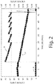
- Apparatus of the above kind has been subjected to tests under real conditions in liquid aluminum in kilns at several test locations. Data saved during these tests included resistor states, discharge current, capacitor voltage, time, and many other parameters. The results of one of such tests are shown in Fig. 2 of the accompanying drawings, in which waveform X shows the measuring current in amps passing between the electrodes during the test period, and waveform Y shows the ultra-capacitor voltage as it discharges during the test period. It can be seen that, despite the decay of the discharge voltage of the ultra-capacitors, the current between the electrodes was maintained in the range of 58 to 63 amps.
Landscapes
- Chemical & Material Sciences (AREA)
- Health & Medical Sciences (AREA)
- Life Sciences & Earth Sciences (AREA)
- General Physics & Mathematics (AREA)
- Pathology (AREA)
- Analytical Chemistry (AREA)
- Biochemistry (AREA)
- General Health & Medical Sciences (AREA)
- Physics & Mathematics (AREA)
- Immunology (AREA)
- Dispersion Chemistry (AREA)
- Engineering & Computer Science (AREA)
- Food Science & Technology (AREA)
- Medicinal Chemistry (AREA)
- Chemical Kinetics & Catalysis (AREA)
- Electrochemistry (AREA)
- Investigating Or Analyzing Materials By The Use Of Electric Means (AREA)
Claims (20)
- Apparat zum Messen einer Reinheit von geschmolzenem Metall, wobei der Apparat umfasst: einen oder mehrere wiederaufladbare Ultrakondensatoren (11 a, 11 b), welche bei einer Entladespannung von 2,7 Volt oder weniger betrieben werden können;
mindestens zwei Elektroden (12a, 12b);
einen Metallreinheit-Messkopf (13), welcher ein Inneres, eine aus einem mit elektrischem Widerstand behafteten Material hergestellte Wand und einen Durchgang (14) in der Wand aufweist, welcher das Innere mit einem Äußeren des Messkopfes (13) verbindet, um geschmolzenen Metall zu erlauben dahindurch hindurchzugehen, wobei eine von den mindestens zwei Elektroden (12a, 12b) in dem Inneren des Messkopfes (13) als eine innere Elektrode und eine andere aus den mindestens zwei Elektroden (12a, 12b) außerhalb des Messkopfes (13) als eine äußere Elektrode positioniert ist;
eine Vorrichtung (V), welche eine Spannung über die innere und die äußere Elektrode registriert und ein Spannungssignal erzeugt;
dadurch gekennzeichnet, dass der Apparat umfasst:für den einen oder für jeden aus dem einen oder den mehreren Ultrakondensatoren (11 a, 11 b) eine zugeordnete Widerstand-Leiternetzwerkschaltung (Na, Nb), welche ihren zugeordneten Ultrakondensator (11 a, 11 b) mit einer aus den Elektroden (12a, 12b) verbindet, wobei die oder jede Widerstand-Leiternetzwerkschaltung (Na, Nb) zwei oder mehr zueinander parallel geschaltete Widerstände (23a, 33a, 43a, 53a, 63a, 73a, 23b, 33b, 43b, 53b, 63b, 73b) umfasst, wobei jeder Widerstand (23a, 33a, 43a, 53a, 63a, 73a, 23b, 33b, 43b, 53b, 63b, 73b) in einem Schaltungsteilstück (22a, 32a, 42a, 52a, 62a, 72a, 22b, 32b, 42b, 52b, 62b, 72b) vorliegt, welches einen oder mehrere Feldeffekttransistoren (21a, 31a, 41a, 51a, 61a, 71a, 21b, 31b, 41b, 51b, 61b, 71b) umfasst, welche in der Lage sind, direkt zwischen einem nichtleitenden AUS-Zustand und einem vollständig leitenden AN-Zustand geschaltet zu werden, und die Widerstand-Leiternetzwerkschaltung oder - Schaltungen (Na, Nb) weisen Widerstandswerte auf, welche wirksam sind, um einen Messstrom von nicht mehr als 100 Ampere durch in dem Durchgang (14) vorliegendes geschmolzenes Metall aufrechtzuerhalten, wenn die Schaltung oder Schaltungen (Na, Nb) der Entladespannung von dem einen oder den mehreren Ultrakondensatoren (11 a, 11 b) ausgesetzt ist/sind; undeine Regelungs-/Steuerungseinheit (18), welche dafür eingerichtet ist, um einzeln die Feldeffekttransistoren (21 a, 31a, 41a, 51a, 61a, 71a, 21b, 31b, 41b, 51b, 61b, 71b) der Schaltungsteilstücke (22a, 32a, 42a, 52a, 62a, 72a, 22b, 32b, 42b, 52b, 62b, 72b) von der oder von jeder Widerstand-Leiternetzwerkschaltung (Na, Nb) zwischen dem nichtleitenden AUS-Zustand und dem vollständig leitenden AN-Zustand gemäß einer Sequenz zu schalten, welche wirksam ist, um den Messstrom innerhalb eines vorbestimmten Strombereichs zumindest für eine Zeit aufrechtzuerhalten, welche für eine Messung einer Reinheit des geschmolzenen Metalls benötigt wird. - Apparat nach Anspruch 1, wobei der Feldeffekttransistor oder die - transistoren (21a, 31a, 41a, 51a, 61a, 71a, 21b, 31b, 41b, 51b, 61b, 71 b) von jedem der Schaltungsteilstücke (22a, 32a, 42a, 52a, 62a, 72a, 22b, 32b, 42b, 52b, 62b, 72b) Flächen-montierte Feldeffekttransistoren sind.
- Apparat nach Anspruch 1 oder Anspruch 2, wobei, wenn in dem vollständig leitenden AN-Zustand, der Feldeffekttransistor oder die - transistoren (21a, 31a, 41a, 51a, 61a, 71a, 21b, 31b, 41b, 51b, 61b, 71 b) von jedem der Schaltungsteilstücke (22a, 32a, 42a, 52a, 62a, 72a, 22b, 32b, 42b, 52b, 62b, 72b) einen Widerstand von weniger als 1 Milliohm in das Schaltungsteilstück (22a, 32a, 42a, 52a, 62a, 72a, 22b, 32b, 42b, 52b, 62b, 72b) einbringen, wobei vorzugsweise mindestens ein Schaltungsteilstück (22a, 32a, 42a, 52a, 62a, 72a, 22b, 32b, 42b, 52b, 62b, 72b) zwei oder mehr der Feldeffekttransistoren (21a, 31a, 41a, 51a, 61a, 71a, 21b, 31b, 41b, 51 b, 61 b, 71 b) umfasst, und wobei die zwei oder mehr Feldeffekttransistoren (21a, 31a, 41a, 51a, 61a, 71a, 21b, 31b, 41b, 51 b, 61 b, 71 b) parallel zueinander geschaltet sind.
- Apparat nach einem der Ansprüche 1 bis 3, wobei die Widerstände (23a, 33a, 43a, 53a, 63a, 73a, 23b, 33b, 43b, 53b, 63b, 73b) von der oder von jeder Widerstand-Leiternetzwerkschaltung (Na, Nb) Widerstandswerte aufweisen, welche voneinander unterschiedlich sind, und wobei die Regelungs-/Steuerungseinheit (18) programmiert ist, die Feldeffekttransistoren (21 a, 31 a, 41 a, 51 a, 61 a, 71 a, 21 b, 31 b, 41 b, 51 b, 61 b, 71 b) der Schaltungsteilstücke (22a, 32a, 42a, 52a, 62a, 72a, 22b, 32b, 42b, 52b, 62b, 72b) zu schalten, um ein Schaltungsteilstück (22a, 32a, 42a, 52a, 62a, 72a, 22b, 32b, 42b, 52b, 62b, 72b) mit niedrigstem Widerstand zuerst einzuschalten und dann, um ein oder mehrere Schaltungsteilstücke (22a, 32a, 42a, 52a, 62a, 72a, 22b, 32b, 42b, 52b, 62b, 72b) mit höherem Widerstand einzuschalten, wenn die Entladespannung von dem mindestens einem Ultrakondensator (11 a, 11 b) während der Zeit absinkt, welche für eine Messung benötigt wird, wobei vorzugsweise die oder jede Widerstand-Leiternetzwerkschaltung (Na, Nb) drei oder mehr Schaltungsteilstücke (22a, 32a, 42a, 52a, 62a, 72a, 22b, 32b, 42b, 52b, 62b, 72b) aufweist und die Regelungs-/Steuerungseinheit (18) programmiert ist, die Schaltungsteilstücke (22a, 32a, 42a, 52a, 62a, 72a, 22b, 32b, 42b, 52b, 62b, 72b) gemäß einer binären Sequenz einzuschalten, wirksam, um den Messstrom innerhalb eines vorbestimmten Strombereichs aufrechtzuerhalten.
- Apparat nach einem der Ansprüche 1 bis 4, wobei die Widerstände (23a, 33a, 43a, 53a, 63a, 73a, 23b, 33b, 43b, 53b, 63b, 73b) jeweils einen Widerstandswert innerhalb eines Bereichs von 0,02 bis 2,64 Ohm aufweisen.
- Apparat nach einem der Ansprüche 1 bis 5, ferner umfassend eine Vorrichtung (17), welche den Messstrom misst und ein Signal erzeugt, die Regelungs-/Steuerungseinheit (18) alarmierend, wenn der Strom auf einen unteren Grenzwert des vorbestimmten Strombereichs fällt.
- Apparat nach einem der Ansprüche 1 bis 6, ferner umfassend einen Spannungssignalanalysator, welcher dazu eingerichtet ist, um eine Metallreinheit aus dem Signal der Vorrichtung zu bestimmen, welche eine Spannung registriert.
- Apparat nach einem der Ansprüche 1 bis 7, ferner umfassend eine Ladeeinheit (16a, 16b) zum Laden des einen oder der mehreren wideraufladbaren Ultrakondensatoren (11 a, 11 b).
- Apparat nach einem der Ansprüche 1 bis 8, aufweisend einen einzelnen Ultrakondensator (11 a, 11 b) und eine einzelne zugeordnete Widerstand-Leiternetzwerkschaltung (Na, Nb).
- Apparat nach einem der Ansprüche 1 bis 8, aufweisend zwei oder mehr Ultrakondensatoren (11 a, 11 b) und zwei oder mehr zugeordnete Widerstand-Leiternetzwerkschaltungen (Na, Nb), wobei der Apparat vorzugsweise eine schaltbare Schaltung umfasst, welche die Ultrakondensatoren (11 a, 11 b) in Reihe schaltet und die Widerstand-Leiternetzwerkschaltungen (Na, Nb) umgeht, um die reihenggeschalteten Ultrakondensatoren (11a, 11 b) über die innere und äußere Elektrode zum Reinigen des Durchgangs (14) zu schalten.
- Apparat nach einem der Ansprüche 1 bis 10, ferner umfassend eine schaltbare Schaltung, welche die oder jede Widerstand-Leiternetzwerkschaltung umgeht und den oder jeden Ultrakondensator direkt über die innere und äußere Elektrode zum Reinigen des Durchgangs (14) schaltet.
- Apparat nach einem der Ansprüche 1 bis 11, wobei die mindestens zwei Elektroden (12a, 12b) nur aus der internen Elektrode und der externen Elektrode bestehen.
- Apparat nach einem der Ansprüche 1 bis 12, wobei der eine oder die mehreren Ultrakondensatoren (11a, 11b), die Widerstände (23a, 33a, 43a, 53a, 63a, 73a, 23b, 33b, 43b, 53b, 63b, 73b) und die Feldeffekttransistoren (21 a, 31 a, 41 a, 51 a, 61 a, 71 a, 21 b, 31 b, 41 b, 51 b, 61 b, 71 b) auf einer Platine direkt benachbart zueinander positioniert sind, um eine Anfälligkeit für einen Rauschempfang zu minimieren.
- Verfahren zum Messen einer Reinheit von geschmolzenem Metall, wobei das Verfahren umfasst:Laden von mindestens einem Ultrakondensator (11 a, 11 b) auf eine Spannung von 2,7 Volt oder weniger;Vorwärtsbewegen von geschmolzenem Metall durch einen Durchgang (14) in einer Wand, welche aus einem mit elektrischem Widerstand behafteten Material hergestellt ist, zwischen einem Inneren und einem Äußeren eines Metallreinheit-Messkopfes (13);Entladen des mindestens einen Ultrakondensators (11a, 11b) über eine Widerstand-Leiternetzwerkschaltung (Na, Nb), welche dem oder jedem Ultrakondensator (11 a, 11 b) zugeordnet ist, durch das geschmolzene Metall, welches sich vorwärts durch den Durchgang (14) bewegt, zwischen einer inneren Elektrode, welche in dem Inneren des Messkopfes (13) positioniert ist, und einer äußeren Elektrode, welche außerhalb des Messkopfes (13) positioniert ist, wobei die oder jede Widerstand-Leiternetzwerkschaltung (Na, Nb) zwei oder mehr zueinander parallel geschaltete Widerstände (23a, 33a, 43a, 53a, 63a, 73a, 23b, 33b, 43b, 53b, 63b, 73b) umfasst, wobei jeder Widerstand (23a, 33a, 43a, 53a, 63a, 73a, 23b, 33b, 43b, 53b, 63b, 73b) in einem Schaltungsteilstück (22a, 32a, 42a, 52a, 62a, 72a, 22b, 32b, 42b, 52b, 62b, 72b) vorliegt, welches einen oder mehrere Feldeffekttransistoren (21 a, 31 a, 41 a, 51 a, 61 a, 71 a, 21 b, 31 b, 41 b, 51 b, 61 b, 71 b) umfasst, welche in der Lage sind, direkt zwischen einem nichtleitenden AUS-Zustand und einem vollständig leitenden AN-Zustand geschaltet zu werden, das Widerstand-Leiternetzwerk (Na, Nb) Widerstandswerte aufweist, welche wirksam sind, um einen Messstrom von nicht mehr als 100 Ampere durch das durch den Durchgang (14) sich vorwärtsbewegende geschmolzene Metall aufrechtzuerhalten;Schalten der Feldeffekttransistoren (21 a, 31 a, 41 a, 51 a, 61 a, 71 a, 21 b, 31 b, 41 b, 51 b, 61 b, 71 b) der Schaltungsteilstücke (22a, 32a, 42a, 52a, 62a, 72a, 22b, 32b, 42b, 52b, 62b, 72b) der oder jeder Widerstand-Leiternetzwerkschaltung (Na, Nb) zwischen dem nichtleitenden AUS-Zustand und dem vollständig leitenden AN-Zustand gemäß einer Sequenz zum Aufrechterhalten des Messstroms innerhalb eines vorbestimmten Strombereichs zumindest für eine Zeit, welche für eine Messung einer Reinheit des geschmolzenen Metalls benötigt wird; undRegistrieren einer Spannung über die interne und die externe Elektrode während der Zeit, welche für eine Messung benötigt wird, Erzeugen eines Spannungssignals und Bestimmen einer Reinheit von dem geschmolzenen Metall aus dem Spannungssignal.
- Verfahren nach Anspruch 14, wobei jede Widerstand-Leiternetzwerkschaltung (Na, Nb) drei oder mehr Schaltungsteilstücke (22a, 32a, 42a, 52a, 62a, 72a, 22b, 32b, 42b, 52b, 62b, 72b) aufweist und das einzelne Schalten der Feldeffekttransistoren (21 a, 31 a, 41 a, 51 a, 61 a, 71 a, 21 b, 31 b, 41 b, 51 b, 61 b, 71 b) der Schaltungsteilstücke (22a, 32a, 42a, 52a, 62a, 72a, 22b, 32b, 42b, 52b, 62b, 72b) der oder jeder Widerstand-Leiternetzwerkschaltung (Na, Nb) gemäß einer binären Sequenz ausgeführt wird, um den Messstrom innerhalb des vorbestimmten Strombereichs aufrechtzuerhalten.
- Verfahren nach Anspruch 14 oder Anspruch 15, wobei die Sequenz vorbestimmt wird gemäß einer Kalibrationsroutine und aufgenommen wird zur Verwendung während der Zeit, welche für eine Messung einer Reinheit des geschmolzenen Metalls benötigt wird.
- Verfahren nach einem der Ansprüche 14 bis 16, wobei der mindestens eine Ultrakondensator (11 a, 11 b) auf eine Spannung von 0,8 bis 1,4 Volt geladen wird.
- Verfahren nach einem der Ansprüche 14 bis 17, wobei die Feldeffekttransistoren (21 a, 31 a, 41 a, 51 a, 61 a, 71 a, 21 b, 31 b, 41 b, 51 b, 61 b, 71 b) in der oder jeder Widerstand-Leiternetzwerkschaltung (Na, Nb) in einer Sequenz geschaltet werden, um den Messstrom in einem vorbestimmten Bereich von 55 bis 65 Ampere, vorzugsweise 60 bis 65 Ampere aufrechterhalten.
- Verfahren nach einem der Ansprüche 14 bis 18, wobei die Feldeffekttransistoren (21 a, 31 a, 41 a, 51 a, 61 a, 71 a, 21 b, 31 b, 41 b, 51 b, 61 b, 71 b) von dem AUS- zu dem AN-Zustand durch von einer Regelungs-/Steuerungseinheit (18) erzeugte Spannungssignale geschaltet werden.
- Verfahren nach einem der Ansprüche 14 bis 19, wobei der Durchgang (14) vor der Zeit, welche für eine Messung einer Reinheit des geschmolzenen Metalls benötigt wird, durch Führen von Strom von dem mindestens einen Ultrakondensator (11 a, 11 b) durch ein geschmolzenes Metall in dem Durchgang (14) gereinigt wird, während veranlasst wird, dass der Strom die oder jede Widerstand-Leiternetzwerkschaltung (Na, Nb) umgeht, wobei das Verfahren vorzugsweise ein Verbinden der zwei Ultrakondensatoren (11 a, 11 b) in Reihe und ein Entladen der reihenggeschalteten Ultrakondensatoren (11a, 11 b) durch den Durchgang (14) umfasst.
Applications Claiming Priority (2)
| Application Number | Priority Date | Filing Date | Title |
|---|---|---|---|
| US201361778028P | 2013-03-12 | 2013-03-12 | |
| PCT/US2014/022768 WO2014159268A1 (en) | 2013-03-12 | 2014-03-10 | Methods of and apparatus for measuring metal cleanliness |
Publications (2)
| Publication Number | Publication Date |
|---|---|
| EP2948752A1 EP2948752A1 (de) | 2015-12-02 |
| EP2948752B1 true EP2948752B1 (de) | 2017-05-03 |
Family
ID=50397324
Family Applications (1)
| Application Number | Title | Priority Date | Filing Date |
|---|---|---|---|
| EP14714522.1A Not-in-force EP2948752B1 (de) | 2013-03-12 | 2014-03-10 | Verfahren und vorrichtung zum messen der sauberkeit von metallen |
Country Status (5)
| Country | Link |
|---|---|
| US (2) | US9389164B2 (de) |
| EP (1) | EP2948752B1 (de) |
| BR (1) | BR112015017282A2 (de) |
| CA (1) | CA2896726C (de) |
| WO (1) | WO2014159268A1 (de) |
Families Citing this family (5)
| Publication number | Priority date | Publication date | Assignee | Title |
|---|---|---|---|---|
| US10411682B2 (en) | 2013-03-12 | 2019-09-10 | Novelis Inc. | Methods of and apparatus for determining particle inclusion and size in molten metal |
| US9716385B2 (en) * | 2014-06-16 | 2017-07-25 | Hamilton Sundstrand Corporation | Solid STTE power controller with parallel MOSFET load sharing |
| CN107046311B (zh) * | 2017-03-30 | 2023-12-12 | 华电电力科学研究院有限公司 | 一种风电机组变桨超级电容内阻补偿的充电回路及其控制方法 |
| CN111122394B (zh) * | 2018-10-31 | 2021-06-08 | 横店集团东磁股份有限公司 | 一种分析铁氧体浆料流延中颗粒形成原因的方法 |
| CN111024772B (zh) * | 2019-12-03 | 2022-06-14 | 西安科技大学 | 激光熔覆熔池微电阻分布成像方法与装置 |
Family Cites Families (19)
| Publication number | Priority date | Publication date | Assignee | Title |
|---|---|---|---|---|
| US3389335A (en) * | 1964-10-19 | 1968-06-18 | Coulter Electronics | Automatic control structure for particle study apparatus |
| US4450435A (en) * | 1981-11-30 | 1984-05-22 | Bobby Dencil James | Analog debris alarm |
| US4555662A (en) | 1983-03-03 | 1985-11-26 | Limca Research Inc. | Method and apparatus for the detection and measurement of particulates in molten metal |
| US4600880A (en) | 1983-03-03 | 1986-07-15 | Limca Research Inc. | Apparatus for the detection and measurement of particulates in molten metal |
| US4775833A (en) * | 1986-10-03 | 1988-10-04 | Coulter Electronics, Inc. | Lodged debris detector for a particle analyzer |
| JPS63238716A (ja) * | 1986-11-14 | 1988-10-04 | Nec Corp | スイッチ回路 |
| CA1315127C (en) * | 1989-02-03 | 1993-03-30 | Raynald Hachey | Apparatus for particle determination in liquid metals |
| CA1328679C (en) * | 1989-05-18 | 1994-04-19 | Raynald Hachey | Apparatus for particle determination in liquid metals |
| US5130883A (en) * | 1990-02-26 | 1992-07-14 | Motorola, Inc. | Circuit for overvoltage protection |
| US5896113A (en) * | 1996-12-20 | 1999-04-20 | Ericsson Inc. | Quadrifilar helix antenna systems and methods for broadband operation in separate transmit and receive frequency bands |
| US6337564B2 (en) | 1999-04-13 | 2002-01-08 | Alcoa Inc. | Detecting and classifying hard and soft inclusions in liquid metal |
| JP4383739B2 (ja) * | 2000-09-12 | 2009-12-16 | ヘレーウス エレクトロ−ナイト インターナシヨナル エヌ ヴイ | 熔融金属中の微粒子の検出及び測定のための装置 |
| DE60305127T2 (de) * | 2002-11-21 | 2006-11-16 | Heraeus Electro-Nite International N.V. | Verbesserte Vorrichtung und Verfahren zur Detektierung und Messung von Partikeln in einer Metallschmelze |
| US7752953B2 (en) | 2003-03-12 | 2010-07-13 | Lsp Technologies, Inc. | Method and system for neutralization of buried mines |
| HUE046599T2 (hu) * | 2004-03-04 | 2020-03-30 | Novelis Inc | Elektród elrendezés folyékony fém tisztaság analizátorhoz |
| US7466156B2 (en) * | 2004-03-25 | 2008-12-16 | International Business Machines Corporation | System of digitally testing an analog driver circuit |
| FR2872518B1 (fr) | 2004-07-02 | 2007-07-27 | Usinor Sa | Procede de controle du bullage en poche et installation de mise en oeuvre |
| KR101589440B1 (ko) | 2009-02-09 | 2016-01-29 | 삼성전자주식회사 | 듀얼 게이트 반도체 장치의 제조 방법 |
| EP2906927B1 (de) * | 2012-10-15 | 2021-08-04 | ABB Inc. | Analysevorrichtung für flüssigmetallreinheit |
-
2014
- 2014-03-10 US US14/203,257 patent/US9389164B2/en active Active
- 2014-03-10 CA CA2896726A patent/CA2896726C/en not_active Expired - Fee Related
- 2014-03-10 EP EP14714522.1A patent/EP2948752B1/de not_active Not-in-force
- 2014-03-10 WO PCT/US2014/022768 patent/WO2014159268A1/en not_active Ceased
- 2014-03-10 BR BR112015017282A patent/BR112015017282A2/pt active Search and Examination
-
2016
- 2016-04-15 US US15/130,530 patent/US9528956B2/en active Active
Also Published As
| Publication number | Publication date |
|---|---|
| US20160231266A1 (en) | 2016-08-11 |
| US9528956B2 (en) | 2016-12-27 |
| US20140266150A1 (en) | 2014-09-18 |
| EP2948752A1 (de) | 2015-12-02 |
| CA2896726A1 (en) | 2014-10-02 |
| CA2896726C (en) | 2017-11-07 |
| US9389164B2 (en) | 2016-07-12 |
| BR112015017282A2 (pt) | 2017-07-11 |
| WO2014159268A1 (en) | 2014-10-02 |
Similar Documents
| Publication | Publication Date | Title |
|---|---|---|
| US9528956B2 (en) | Methods of and apparatus for measuring metal cleanliness | |
| KR102216324B1 (ko) | 접촉자의 유지 보수 방법 및 검사 장치 | |
| US20170131363A1 (en) | Improved Battery Testing Device | |
| KR20110034580A (ko) | 시험 장치, 부가 회로 및 시험용 보드 | |
| US9476850B2 (en) | Electrode configuration for LiMCA | |
| GB2530716A (en) | Cascade circuit tester | |
| CA2896727C (en) | Methods of and apparatus for determining particle inclusion and size in molten metal | |
| JP4844650B2 (ja) | スポット溶接検査装置およびスポット溶接検査方法 | |
| JP2020190510A (ja) | 基板寿命監視装置および基板寿命遠隔監視システム | |
| RU2252118C2 (ru) | Датчик тока сварки | |
| MXPA06009915A (en) | Electrode configuration for limca |
Legal Events
| Date | Code | Title | Description |
|---|---|---|---|
| PUAI | Public reference made under article 153(3) epc to a published international application that has entered the european phase |
Free format text: ORIGINAL CODE: 0009012 |
|
| 17P | Request for examination filed |
Effective date: 20150828 |
|
| AK | Designated contracting states |
Kind code of ref document: A1 Designated state(s): AL AT BE BG CH CY CZ DE DK EE ES FI FR GB GR HR HU IE IS IT LI LT LU LV MC MK MT NL NO PL PT RO RS SE SI SK SM TR |
|
| AX | Request for extension of the european patent |
Extension state: BA ME |
|
| DAX | Request for extension of the european patent (deleted) | ||
| R17P | Request for examination filed (corrected) |
Effective date: 20150828 |
|
| GRAP | Despatch of communication of intention to grant a patent |
Free format text: ORIGINAL CODE: EPIDOSNIGR1 |
|
| INTG | Intention to grant announced |
Effective date: 20161013 |
|
| GRAS | Grant fee paid |
Free format text: ORIGINAL CODE: EPIDOSNIGR3 |
|
| GRAA | (expected) grant |
Free format text: ORIGINAL CODE: 0009210 |
|
| AK | Designated contracting states |
Kind code of ref document: B1 Designated state(s): AL AT BE BG CH CY CZ DE DK EE ES FI FR GB GR HR HU IE IS IT LI LT LU LV MC MK MT NL NO PL PT RO RS SE SI SK SM TR |
|
| REG | Reference to a national code |
Ref country code: GB Ref legal event code: FG4D |
|
| REG | Reference to a national code |
Ref country code: AT Ref legal event code: REF Ref document number: 890518 Country of ref document: AT Kind code of ref document: T Effective date: 20170515 Ref country code: CH Ref legal event code: EP Ref country code: CH Ref legal event code: NV Representative=s name: E. BLUM AND CO. AG PATENT- UND MARKENANWAELTE , CH |
|
| REG | Reference to a national code |
Ref country code: IE Ref legal event code: FG4D |
|
| REG | Reference to a national code |
Ref country code: DE Ref legal event code: R096 Ref document number: 602014009329 Country of ref document: DE |
|
| REG | Reference to a national code |
Ref country code: NL Ref legal event code: MP Effective date: 20170503 |
|
| REG | Reference to a national code |
Ref country code: LT Ref legal event code: MG4D |
|
| REG | Reference to a national code |
Ref country code: NO Ref legal event code: T2 Effective date: 20170503 |
|
| PG25 | Lapsed in a contracting state [announced via postgrant information from national office to epo] |
Ref country code: HR Free format text: LAPSE BECAUSE OF FAILURE TO SUBMIT A TRANSLATION OF THE DESCRIPTION OR TO PAY THE FEE WITHIN THE PRESCRIBED TIME-LIMIT Effective date: 20170503 Ref country code: ES Free format text: LAPSE BECAUSE OF FAILURE TO SUBMIT A TRANSLATION OF THE DESCRIPTION OR TO PAY THE FEE WITHIN THE PRESCRIBED TIME-LIMIT Effective date: 20170503 Ref country code: GR Free format text: LAPSE BECAUSE OF FAILURE TO SUBMIT A TRANSLATION OF THE DESCRIPTION OR TO PAY THE FEE WITHIN THE PRESCRIBED TIME-LIMIT Effective date: 20170804 Ref country code: FI Free format text: LAPSE BECAUSE OF FAILURE TO SUBMIT A TRANSLATION OF THE DESCRIPTION OR TO PAY THE FEE WITHIN THE PRESCRIBED TIME-LIMIT Effective date: 20170503 Ref country code: LT Free format text: LAPSE BECAUSE OF FAILURE TO SUBMIT A TRANSLATION OF THE DESCRIPTION OR TO PAY THE FEE WITHIN THE PRESCRIBED TIME-LIMIT Effective date: 20170503 |
|
| PG25 | Lapsed in a contracting state [announced via postgrant information from national office to epo] |
Ref country code: SE Free format text: LAPSE BECAUSE OF FAILURE TO SUBMIT A TRANSLATION OF THE DESCRIPTION OR TO PAY THE FEE WITHIN THE PRESCRIBED TIME-LIMIT Effective date: 20170503 Ref country code: IS Free format text: LAPSE BECAUSE OF FAILURE TO SUBMIT A TRANSLATION OF THE DESCRIPTION OR TO PAY THE FEE WITHIN THE PRESCRIBED TIME-LIMIT Effective date: 20170903 Ref country code: BG Free format text: LAPSE BECAUSE OF FAILURE TO SUBMIT A TRANSLATION OF THE DESCRIPTION OR TO PAY THE FEE WITHIN THE PRESCRIBED TIME-LIMIT Effective date: 20170803 Ref country code: RS Free format text: LAPSE BECAUSE OF FAILURE TO SUBMIT A TRANSLATION OF THE DESCRIPTION OR TO PAY THE FEE WITHIN THE PRESCRIBED TIME-LIMIT Effective date: 20170503 Ref country code: PL Free format text: LAPSE BECAUSE OF FAILURE TO SUBMIT A TRANSLATION OF THE DESCRIPTION OR TO PAY THE FEE WITHIN THE PRESCRIBED TIME-LIMIT Effective date: 20170503 Ref country code: LV Free format text: LAPSE BECAUSE OF FAILURE TO SUBMIT A TRANSLATION OF THE DESCRIPTION OR TO PAY THE FEE WITHIN THE PRESCRIBED TIME-LIMIT Effective date: 20170503 Ref country code: NL Free format text: LAPSE BECAUSE OF FAILURE TO SUBMIT A TRANSLATION OF THE DESCRIPTION OR TO PAY THE FEE WITHIN THE PRESCRIBED TIME-LIMIT Effective date: 20170503 |
|
| PG25 | Lapsed in a contracting state [announced via postgrant information from national office to epo] |
Ref country code: EE Free format text: LAPSE BECAUSE OF FAILURE TO SUBMIT A TRANSLATION OF THE DESCRIPTION OR TO PAY THE FEE WITHIN THE PRESCRIBED TIME-LIMIT Effective date: 20170503 Ref country code: DK Free format text: LAPSE BECAUSE OF FAILURE TO SUBMIT A TRANSLATION OF THE DESCRIPTION OR TO PAY THE FEE WITHIN THE PRESCRIBED TIME-LIMIT Effective date: 20170503 Ref country code: SK Free format text: LAPSE BECAUSE OF FAILURE TO SUBMIT A TRANSLATION OF THE DESCRIPTION OR TO PAY THE FEE WITHIN THE PRESCRIBED TIME-LIMIT Effective date: 20170503 Ref country code: RO Free format text: LAPSE BECAUSE OF FAILURE TO SUBMIT A TRANSLATION OF THE DESCRIPTION OR TO PAY THE FEE WITHIN THE PRESCRIBED TIME-LIMIT Effective date: 20170503 Ref country code: CZ Free format text: LAPSE BECAUSE OF FAILURE TO SUBMIT A TRANSLATION OF THE DESCRIPTION OR TO PAY THE FEE WITHIN THE PRESCRIBED TIME-LIMIT Effective date: 20170503 |
|
| REG | Reference to a national code |
Ref country code: DE Ref legal event code: R097 Ref document number: 602014009329 Country of ref document: DE |
|
| PG25 | Lapsed in a contracting state [announced via postgrant information from national office to epo] |
Ref country code: IT Free format text: LAPSE BECAUSE OF FAILURE TO SUBMIT A TRANSLATION OF THE DESCRIPTION OR TO PAY THE FEE WITHIN THE PRESCRIBED TIME-LIMIT Effective date: 20170503 Ref country code: SM Free format text: LAPSE BECAUSE OF FAILURE TO SUBMIT A TRANSLATION OF THE DESCRIPTION OR TO PAY THE FEE WITHIN THE PRESCRIBED TIME-LIMIT Effective date: 20170503 |
|
| PLBE | No opposition filed within time limit |
Free format text: ORIGINAL CODE: 0009261 |
|
| STAA | Information on the status of an ep patent application or granted ep patent |
Free format text: STATUS: NO OPPOSITION FILED WITHIN TIME LIMIT |
|
| REG | Reference to a national code |
Ref country code: FR Ref legal event code: PLFP Year of fee payment: 5 |
|
| 26N | No opposition filed |
Effective date: 20180206 |
|
| PG25 | Lapsed in a contracting state [announced via postgrant information from national office to epo] |
Ref country code: SI Free format text: LAPSE BECAUSE OF FAILURE TO SUBMIT A TRANSLATION OF THE DESCRIPTION OR TO PAY THE FEE WITHIN THE PRESCRIBED TIME-LIMIT Effective date: 20170503 |
|
| GBPC | Gb: european patent ceased through non-payment of renewal fee |
Effective date: 20180310 |
|
| PG25 | Lapsed in a contracting state [announced via postgrant information from national office to epo] |
Ref country code: MC Free format text: LAPSE BECAUSE OF FAILURE TO SUBMIT A TRANSLATION OF THE DESCRIPTION OR TO PAY THE FEE WITHIN THE PRESCRIBED TIME-LIMIT Effective date: 20170503 |
|
| REG | Reference to a national code |
Ref country code: BE Ref legal event code: MM Effective date: 20180331 |
|
| REG | Reference to a national code |
Ref country code: IE Ref legal event code: MM4A |
|
| PG25 | Lapsed in a contracting state [announced via postgrant information from national office to epo] |
Ref country code: LU Free format text: LAPSE BECAUSE OF NON-PAYMENT OF DUE FEES Effective date: 20180310 |
|
| PG25 | Lapsed in a contracting state [announced via postgrant information from national office to epo] |
Ref country code: IE Free format text: LAPSE BECAUSE OF NON-PAYMENT OF DUE FEES Effective date: 20180310 |
|
| PG25 | Lapsed in a contracting state [announced via postgrant information from national office to epo] |
Ref country code: BE Free format text: LAPSE BECAUSE OF NON-PAYMENT OF DUE FEES Effective date: 20180331 Ref country code: GB Free format text: LAPSE BECAUSE OF NON-PAYMENT OF DUE FEES Effective date: 20180310 |
|
| REG | Reference to a national code |
Ref country code: AT Ref legal event code: UEP Ref document number: 890518 Country of ref document: AT Kind code of ref document: T Effective date: 20170503 |
|
| PG25 | Lapsed in a contracting state [announced via postgrant information from national office to epo] |
Ref country code: MT Free format text: LAPSE BECAUSE OF NON-PAYMENT OF DUE FEES Effective date: 20180310 |
|
| PG25 | Lapsed in a contracting state [announced via postgrant information from national office to epo] |
Ref country code: TR Free format text: LAPSE BECAUSE OF FAILURE TO SUBMIT A TRANSLATION OF THE DESCRIPTION OR TO PAY THE FEE WITHIN THE PRESCRIBED TIME-LIMIT Effective date: 20170503 |
|
| PGFP | Annual fee paid to national office [announced via postgrant information from national office to epo] |
Ref country code: AT Payment date: 20200227 Year of fee payment: 7 Ref country code: DE Payment date: 20200218 Year of fee payment: 7 Ref country code: NO Payment date: 20200225 Year of fee payment: 7 |
|
| PG25 | Lapsed in a contracting state [announced via postgrant information from national office to epo] |
Ref country code: PT Free format text: LAPSE BECAUSE OF FAILURE TO SUBMIT A TRANSLATION OF THE DESCRIPTION OR TO PAY THE FEE WITHIN THE PRESCRIBED TIME-LIMIT Effective date: 20170503 |
|
| PGFP | Annual fee paid to national office [announced via postgrant information from national office to epo] |
Ref country code: CH Payment date: 20200221 Year of fee payment: 7 |
|
| PG25 | Lapsed in a contracting state [announced via postgrant information from national office to epo] |
Ref country code: HU Free format text: LAPSE BECAUSE OF FAILURE TO SUBMIT A TRANSLATION OF THE DESCRIPTION OR TO PAY THE FEE WITHIN THE PRESCRIBED TIME-LIMIT; INVALID AB INITIO Effective date: 20140310 Ref country code: CY Free format text: LAPSE BECAUSE OF FAILURE TO SUBMIT A TRANSLATION OF THE DESCRIPTION OR TO PAY THE FEE WITHIN THE PRESCRIBED TIME-LIMIT Effective date: 20170503 Ref country code: MK Free format text: LAPSE BECAUSE OF NON-PAYMENT OF DUE FEES Effective date: 20170503 |
|
| PGFP | Annual fee paid to national office [announced via postgrant information from national office to epo] |
Ref country code: FR Payment date: 20200220 Year of fee payment: 7 |
|
| PG25 | Lapsed in a contracting state [announced via postgrant information from national office to epo] |
Ref country code: AL Free format text: LAPSE BECAUSE OF FAILURE TO SUBMIT A TRANSLATION OF THE DESCRIPTION OR TO PAY THE FEE WITHIN THE PRESCRIBED TIME-LIMIT Effective date: 20170503 |
|
| REG | Reference to a national code |
Ref country code: DE Ref legal event code: R119 Ref document number: 602014009329 Country of ref document: DE |
|
| REG | Reference to a national code |
Ref country code: NO Ref legal event code: MMEP |
|
| REG | Reference to a national code |
Ref country code: CH Ref legal event code: PL |
|
| REG | Reference to a national code |
Ref country code: AT Ref legal event code: MM01 Ref document number: 890518 Country of ref document: AT Kind code of ref document: T Effective date: 20210310 |
|
| PG25 | Lapsed in a contracting state [announced via postgrant information from national office to epo] |
Ref country code: DE Free format text: LAPSE BECAUSE OF NON-PAYMENT OF DUE FEES Effective date: 20211001 Ref country code: FR Free format text: LAPSE BECAUSE OF NON-PAYMENT OF DUE FEES Effective date: 20210331 Ref country code: LI Free format text: LAPSE BECAUSE OF NON-PAYMENT OF DUE FEES Effective date: 20210331 Ref country code: AT Free format text: LAPSE BECAUSE OF NON-PAYMENT OF DUE FEES Effective date: 20210310 Ref country code: CH Free format text: LAPSE BECAUSE OF NON-PAYMENT OF DUE FEES Effective date: 20210331 Ref country code: NO Free format text: LAPSE BECAUSE OF NON-PAYMENT OF DUE FEES Effective date: 20210331 |