EP2950476B1 - Verfahren und vorrichtung für verbesserte höherwertige modulation - Google Patents
Verfahren und vorrichtung für verbesserte höherwertige modulation Download PDFInfo
- Publication number
- EP2950476B1 EP2950476B1 EP15167526.1A EP15167526A EP2950476B1 EP 2950476 B1 EP2950476 B1 EP 2950476B1 EP 15167526 A EP15167526 A EP 15167526A EP 2950476 B1 EP2950476 B1 EP 2950476B1
- Authority
- EP
- European Patent Office
- Prior art keywords
- sin
- cos
- bit
- constellation
- bit positions
- Prior art date
- Legal status (The legal status is an assumption and is not a legal conclusion. Google has not performed a legal analysis and makes no representation as to the accuracy of the status listed.)
- Active
Links
Images






Classifications
-
- H—ELECTRICITY
- H04—ELECTRIC COMMUNICATION TECHNIQUE
- H04L—TRANSMISSION OF DIGITAL INFORMATION, e.g. TELEGRAPHIC COMMUNICATION
- H04L27/00—Modulated-carrier systems
- H04L27/32—Carrier systems characterised by combinations of two or more of the types covered by groups H04L27/02, H04L27/10, H04L27/18 or H04L27/26
- H04L27/34—Amplitude- and phase-modulated carrier systems, e.g. quadrature-amplitude modulated carrier systems
-
- H—ELECTRICITY
- H04—ELECTRIC COMMUNICATION TECHNIQUE
- H04L—TRANSMISSION OF DIGITAL INFORMATION, e.g. TELEGRAPHIC COMMUNICATION
- H04L1/00—Arrangements for detecting or preventing errors in the information received
- H04L1/004—Arrangements for detecting or preventing errors in the information received by using forward error control
-
- H—ELECTRICITY
- H04—ELECTRIC COMMUNICATION TECHNIQUE
- H04L—TRANSMISSION OF DIGITAL INFORMATION, e.g. TELEGRAPHIC COMMUNICATION
- H04L1/00—Arrangements for detecting or preventing errors in the information received
- H04L1/004—Arrangements for detecting or preventing errors in the information received by using forward error control
- H04L1/0056—Systems characterized by the type of code used
- H04L1/0071—Use of interleaving
-
- H—ELECTRICITY
- H04—ELECTRIC COMMUNICATION TECHNIQUE
- H04L—TRANSMISSION OF DIGITAL INFORMATION, e.g. TELEGRAPHIC COMMUNICATION
- H04L25/00—Baseband systems
- H04L25/02—Details ; arrangements for supplying electrical power along data transmission lines
- H04L25/03—Shaping networks in transmitter or receiver, e.g. adaptive shaping networks
- H04L25/03006—Arrangements for removing intersymbol interference
- H04L25/03178—Arrangements involving sequence estimation techniques
- H04L25/03312—Arrangements specific to the provision of output signals
Definitions
- a signal constellation diagram is a representation of a signal modulated by a digital modulation scheme, such as quadrature amplitude modulation or phase-shift keying.
- the signal constellation depicts the signal as a two-dimensional scatter diagram, in the complex plane, at symbol sampling instants. In other words, the signal constellation represents the possible symbols that may be selected by a given modulation scheme as points in the complex plane. Accordingly, a modulated waveform, from a set of data symbols, leads to the concept of a signal constellation.
- FEC forward error correction
- Well-known classical examples of higher order modulation signals include 8-PSK, 16-QAM, 32-QAM and 64-QAM, which are capable of sending 3, 4, 5 and 6 bits, respectively, per symbol.
- the 16-QAM, 32-QAM and 64-QAM signals are often modified by organizing them to several rings of different amplitudes.
- the Digital Video Broadcast via Satellites standard (DVB-S2) employs 16-APSK and 32-APSK modulation signals, where the 16-APSK employs a signal constellation of two rings, with 4 and 12 possible phase positions, respectively, and the 32-APSK employs a signal constellation of three rings, with 4, 12 and 16 possible phase positions, respectively. As such, they are also called 4+12-APSK and 4+12+16-APSK, respectively.
- US 2011/0164705 A1 discloses an interleaver and a 32APSK modulator.
- the interleaving scheme is not disclosed in detail.
- An uniform swapping of one or more bit positions with one or more corresponding other bit positions in each bit label and a shifting of all bit levels is also not described and is thus not integrated in the 32APSK modulation.
- the present invention advantageously addresses the needs above, as well as other needs, by providing methods, systems and software for high order signal modulation based on improved signal constellation and bit labeling designs for enhanced performance characteristics, including decreased power consumption.
- methods and apparatuses are provided for modulation and demodulation of signals based on an 8-ary, 1+7APSK signal constellation of improved bit labeling and coordinates.
- methods and apparatuses are provided for modulation and demodulation of signals based on a 16-ary, 6+10APSK signal constellation of improved bit labeling and coordinates.
- methods and apparatuses are provided for modulation and demodulation of signals based on a 32-ary, 16+16APSK signal constellation and two 32-ary, 4+12+16APSK signal constellations of improved bit labeling and coordinates.
- methods and apparatuses are provided for modulation and demodulation of signals based on a 64-ary, 8+16+20+20APSK signal constellation of improved bit labeling and coordinates, and a 64-ary 12+16+16+20 signal constellation.
- FIGs. 1A and 1B illustrate communications systems capable of utilizing constellation and bit labeling designs according to various exemplary embodiments of the present invention.
- a digital communications system 110 includes one or more transmitters 111 (of which one is shown) that generate signal waveforms across a communication channel 113 to one or more receivers 115 (of which one is shown).
- the transmitter 111 has a message source that produces a discrete set of possible messages, where each of the possible messages has a corresponding signal waveform.
- These signal waveforms are attenuated, or otherwise altered, by communications channel 113.
- coding is utilized. For example, forward error correction (FEC) codes can be employed.
- FEC forward error correction
- FEC is required in terrestrial and satellite systems to provide high quality communication over a radio frequency (RF) propagation channel, which induces signal waveform and spectrum distortions, including signal attenuation (freespace propagation loss), multi-path induced fading and adjacent channel interference.
- RF radio frequency
- exemplary design objectives include selecting modulation formats, error control schemes, demodulation and decoding techniques and hardware components that together provide an efficient balance between system performance and implementation complexity. Differences in propagation channel characteristics, such as between terrestrial and satellite communication channels, naturally result in significantly different system designs. Likewise, existing communications systems continue to evolve in order to satisfy increased system requirements for new higher rate or higher fidelity communication services.
- FIG. 1B is a diagram of an exemplary satellite communications system 120 capable of supporting communication among terminals with varied capabilities, according to an embodiment of the present invention.
- Satellite communications system 120 includes a satellite 121 that supports communication among multiple satellite terminals (STs) 123, 125 and a hub 127.
- the HUB 127 may assume the role of a Network Operations Center (NOC), which controls the access of the STs 123, 125 to the system 120 and also provides element management functions and control of the address resolution and resource management functionality.
- NOC Network Operations Center
- the Satellite communications system 120 may operate as a traditional bent-pipe system, where the satellite essentially operates as a repeater. Alternatively, the system 120 may employ a switching or processing satellite supporting mesh communications (point-to-point communications directly between, for example, the two STs 123 and 125).
- the satellite operates as a repeater or bent pipe, and communications between the ST's 123 and 125 are transmitted over a double-hop path.
- the communication is transmitted, via the satellite, from the ST 123 to the HUB 127.
- the HUB 127 decodes the communication and determines the destination ST 125.
- the HUB 127 then appropriately addresses and repackages the communication, encodes and modulates it, and transmits the communication over the second hop, via the satellite, to the destination ST 125.
- the satellite of such a system acts as a bent pipe or repeater, transmitting communications between the HUB 127 and the STs.
- the system may support direct unicast (point-to-point) communications and multicast communications among the STs 123, 125.
- the satellite 121 decodes the received signal and determines the destination ST or STs (as the hub 127 would in a bent-pipe system).
- the satellite 121 addresses the data accordingly, encodes and modulates it, and transmits the modulated signal, over the channel 113, to the destination ST or STs (e.g., ST 125)
- the STs 123, 125 provide connectivity to one or more hosts 129, 131, respectively.
- the system 120 has a fully meshed architecture, whereby the STs 123, 125 may directly communicate.
- the common air interface needs to support a discovery of the terminal's capabilities profile (or context information).
- These capabilities can include encryption scheme, compression scheme, segmentation and reassembly (SAR) scheme, automatic repeat request (ARQ) scheme, Quality-of-Service (QoS) parameters, power levels, modulation and coding schemes, power control algorithms, and link adaptation capabilities.
- terminal profile can be readily exchanged over a network with a star topology where no peer-to-peer communication exists.
- capabilities profiles include a packet data protocol (PDP) context and a mobility management context.
- PDP packet data protocol
- mobility management context the concepts of PDP context and mobility management context are combined and the term packet data protocol (PDP) context is used in general to refer to terminal capabilities. It is recognized that these terminals can be mobile as well as non-mobile.
- the exchange of terminal profile can be executed over a meshed network, in a peer-to-peer manner.
- the STs 123, 125 support the use of a negotiation procedure to determine the optimal configuration for transmission and reception of data. If a protocol implements control procedures or options in newer versions (i.e., flow-control/rate-control), older protocol versions are able to detect the initiation as a new unsupported procedure and report the same to the peer with minimal disruption in the flow of traffic.
- the ST-ST protocol advantageously takes into account that even for peers of the same version, some capabilities may not necessarily be always supported due to local temporal processing/memory/congestion-related constraints. Additionally, the ST-ST protocol design provides for rapid developments in data communication technology. For each ST 123, 125, there exist some configuration information, including network configuration, network service provider (NSP) configuration, software configuration, and user configuration, as indicated by the NOC 127. These configurations relate to the features that the ST 123, 125 supports and offers to the user, and have a direct bearing on the transmission and reception capabilities.
- NSP network service provider
- a packet transfer context is employed. Such a common feature set depends on the PDP contexts of the two STs 123, 125. Further, this common feature set may also depend on the QoS of the flow, as well as the loading and status of the two STs at that point of time.
- the packet transfer context is unidirectional and valid only for the transmit ST to send packets to the specified receive ST; thus, the packet transfer context may be unique to a given pair of STs.
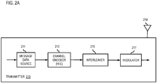
- FIG. 2A illustrates a block diagram of an exemplary transmitter 210 configured to operate in the systems of FIGs. 1A and 1B , in accordance with exemplary embodiments of the present invention.
- the transmitter 210 is equipped with a channel encoder (FEC encoder) 213 that accepts input from a data source 211 and outputs coded stream of higher redundancy suitable for error correction processing at the receiver (shown in FIG. 2B ).
- FEC encoder channel encoder
- the encoder 213 generates the coded stream, and passes it to an interleaver 215, which reorders the sequence of symbols or bits from the encoder in a predetermined manner.
- the interleaved signal is fed to a modulator 217, which maps the encoded messages to signal waveforms, based in part on the signal constellations in accordance with the various exemplary embodiments of the present invention.
- the signal waveforms are then transmitted, via the transmit antenna 219, over the communication channel 113 to the satellite 121.
- Binary FEC codes can effectively be used by the channel encoder 213 with any high order modulation of the modulator 217, which eliminates the need for modulation specific trellis coded modulation (or its derivatives), and hence greatly simplifies implementation.
- LDPC low density parity check
- the role of the bit interleaver 215 is unique in the context of designing DVB-S2 codes. In that context, the bit interleaver facilitates the assignment of LDPC bit nodes of varying degrees to high order modulation bits of varying vulnerability to channel noise. An appropriately chosen bit interleaver thus achieves significant performance improvement when LDPC codes are used.
- FIG. 2B illustrates a block diagram of an exemplary receiver configured to operate in the systems of FIGs. 1A and 1B , in accordance with exemplary embodiments of the present invention.
- the receiver comprises receive antenna 229, demodulator 227, de-interleaver 225 and channel decoder 223.
- the receive antenna 229 receives the signal waveform transmitted over the channel 113 from the satellite 121.
- the demodulator 227 demodulates the received signal waveforms, based in part on the signal constellation, of the various embodiments of the present invention, employed for the modulation, to obtain the encoded signals.
- the de-interleaver reorders the sequence of symbols or bits based on the predetermined manner of interleaving at the transmitter 210.
- the channel decoder then decodes the de-interleaved bit sequence to generate the message data 221.
- the modulator 217 can generate a modulated waveform from any set of data symbols, leading to the concept of a signal constellation.
- Each distinct point in the signal constellation corresponds to a different modulated waveform, where all waveforms share the same set of basis functions.
- the component of the i th vector x i , along the n th basis function ⁇ n ( t ) is denoted x in .
- the occurrence of a particular data symbol in the constellation determines the probability of the i th vector (and thus of the i th waveform), p x ( i ) .
- the constellation diagram shows the phases of the symbols and their relationship to each other.
- the x-axis projection for each symbol represents the I-channel amplitude, and the y-axis projection for each symbol represents the Q-channel amplitude.
- the power available in a communication system limits the average amount of energy required to transmit each successive data symbol. Accordingly, the concept of average energy represents an important concept for a signal constellation.
- Minimization of power requirements reduces burdens on the transmitter design (e.g., component costs, size, thermal issues, etc.).
- a reduction in power consumption e.g., energy per symbol leaves room for increased transmission throughput.
- the goal of the signal constellation design is to optimally arrange the points in a vector space with minimum average energy, while maintaining at least a minimum distance between each pair of points.
- an 8-ary, 1+7APSK constellation, with associated bit labeling is shown in FIG. 3A .
- the first number (1) denotes the number of constellation points on the inner ring (in this case the origin), and the second number (7) denotes the number of constellation points on the outer ring.
- the bit positioning for the signal constellation of FIG. 3A is shown in FIG. 3A .
- the transmitter 210 of an ST 123 may be configured to modulate one or more signals based on the signal constellation of FIG. 3A .
- the ST 123 would then transmit the modulated signal over the channel 113 to the satellite 121.
- the satellite 121 as a bent-pipe satellite, may then transmit the signal over the channel 113, through the hub 127, to the destination ST or STs (e.g., ST 125).
- the satellite 121 as a processing satellite, may decode the signal to determine the destination ST or ST's, address the data accordingly, and re-encode and modulate the data, and transmit the modulated signal directly to the destination ST or STs (e.g., ST 125).
- the system 120 can achieve enhanced performance, such as decreased power consumption and/or enhanced throughput.
- the 1+7APSK constellation achieves significant performance improvements over, for example, the DVB-S2 8-PSK constellation (approximately 0.6dB with a 2/3 rate FEC code, and approximately 0.8 dB with an 8/9 rate code). Further, as is evident from the performance curves of FIG. 3D , the 1+7APSK constellation also achieves significant performance improvements with an iterative receiver as compared to a non-iterative receiver (approximately 0.5 dB).
- the optimal labeling and bit positions illustrated in FIG. 3A are not unique in that certain specific modifications of bit labeling and bit positioning can achieve equivalent performance.
- One such modification exists with respect to the bit positions, whereby equivalent performance can be achieved with a 1+7APSK signal constellation as shown in FIG. 3A , but where each of the [x, y] bit positions is rotated by a fixed rotation factor (e.g., each bit position is rotated by the same rotation factor, such as 5 degrees, 7 degrees, 12 degrees, etc.).
- bit labeling is modified by interchanging the 0's and 1's (changing each one to a zero and changing each zero to a one in each bit label) and/or by applying a uniform swapping of bit positions within each bit label (uniformly swapping one or more bit positions with one or more corresponding other bit positions in each bit label - e.g., swapping the first and third bit label positions within each bit label).
- bit labeling is modified by interchanging the 0's and 1's (changing each one to a zero and changing each zero to a one in each bit label) and/or by applying a uniform swapping of bit positions within each bit label (uniformly swapping one or more bit positions with one or more corresponding other bit positions in each bit label - e.g., swapping the first and third bit label positions within each bit label).
- any of the foregoing specific modifications can either be applied by itself or in combination with any one or more of the other specific modifications.
- FIG. 4A a 16-ary, 6+10APSK constellation, with associated bit labeling, is shown in FIG. 4A .
- 6+10APSK the first number (6) denotes the number of constellation points on the inner ring, and the second number (10) denotes the number of constellation points on the outer ring.
- bit positioning for the signal constellation of FIG. 4A the bit positioning for the signal constellation of FIG.
- FIG. 3C depicts the performance curves of FIG. 3C , with a 3/4 rate FEC code, the 6+10APSK constellation of FIG.
- the 6+10APSK constellation of FIG. 4A achieves significant performance improvements over, for example, the DVB-S2 4+12APSK constellation (approximately 0.1dB with a non-iterative receiver, and approximately 0.3 dB with an iterative receiver). Further, as is evident from the performance curves of FIG. 3D , the 6+10APSK constellation of FIG. 4A also achieves significant performance improvements over the DVB-S2 4+12APSK constellation, for example, with a 9/10 rate FEC code (approximately 0.13dB with a non-iterative receiver, and approximately 0.35 dB with an iterative receiver). Accordingly, here also, in the case of the 6+10APSK constellation, the iterative receiver achieves significant performance improvements with an iterative receiver as compared with a non-iterative receiver.
- a system 120 can achieve enhanced performance, such as decreased power consumption and/or enhanced throughput.
- the optimal labeling and bit positions illustrated in FIG. 4A are not unique in that the above-specified modifications of the bit labeling and bit positioning can achieve equivalent performance.
- equivalent performance can be achieved with a 6+10APSK signal constellation as shown in FIG. 4A , but where each of the [x, y] bit positions is rotated by a fixed rotation factor (e.g., each bit position is rotated by the same rotation factor).
- bit labeling equivalent performance can be achieved with a 6+10APSK signal constellation as shown in FIG. 4A , but where the bit labeling is modified by interchanging the 0's and 1's, and/or by applying a uniform swapping of bit positions within each bit label (e.g., swapping the first and third bit label positions within each bit label).
- bit labeling is modified by interchanging the 0's and 1's, and/or by applying a uniform swapping of bit positions within each bit label (e.g., swapping the first and third bit label positions within each bit label).
- any of the foregoing specific modifications can either be applied by itself or in combination with any one or more of the other specific modifications.
- a 32-ary, 16+16APSK constellation, with associated bit labeling is shown in FIG. 5A .
- 16+16APSK the first number (16) denotes the number of constellation points on the inner ring, and the second number (16) denotes the number of constellation points on the outer ring.
- the bit positioning for the signal constellation of FIG. 5A is shown in FIG. 5A .
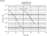
- FIG. 5B depicts the performance (based on an LDPC code of 3.333 bits/symbol) for the 16+16APSK constellation of FIG. 5A , with respect to the theoretical capacity; as compared with performance curves for the DVB-S2 4+12+16APSK constellation, and the DVB-S2 4+12APSK constellation.
- the 16+16APSK constellation of FIG. 5A achieves significant performance improvements over, for example, the DVB-S2 4+12+16APSK constellation (approximately 0.65dB).
- a system 120 can achieve enhanced performance, such as decreased power consumption and/or enhanced throughput.
- the optimal labeling and bit positions illustrated in FIG. 5A are not unique in that the above-specified modifications of the bit labeling and bit positioning can achieve equivalent performance.
- equivalent performance can be achieved with a 16+16APSK signal constellation as shown in FIG. 5A , but where each of the [x, y] bit positions is rotated by a fixed rotation factor (e.g., each bit position is rotated by the same rotation factor).
- bit labeling equivalent performance can be achieved with a 16+16APSK signal constellation as shown in FIG. 5A , but where the bit labeling is modified by interchanging the 0's and 1's, and/or by applying a uniform swapping of bit positions within each bit label (e.g., swapping the first and third bit label positions within each bit label).
- bit labeling is modified by interchanging the 0's and 1's, and/or by applying a uniform swapping of bit positions within each bit label (e.g., swapping the first and third bit label positions within each bit label).
- any of the foregoing specific modifications can either be applied by itself or in combination with any one or more of the other specific modifications.
- a 32-ary, 4+12+16APSK constellation, with associated bit labeling is shown in FIG. 6A .
- the first number (4) denotes the number of constellation points on the inner-most ring
- the second number (12) denotes the number of constellation points on the next ring
- the third number (16) denotes the number of constellation points on the outer ring.
- a 32-ary, 4+12+16APSK constellation, with associated bit labeling is shown in FIG. 6B .
- the first number (4) denotes the number of constellation points on the inner-most ring
- the second number (12) denotes the number of constellation points on the next ring
- the third number (16) denotes the number of constellation points on the outer ring.
- 6A and 6B also achieve significant performance improvements over the DVB-S2 4+12+16APSK constellation, for example, with a 4/5 rate FEC code (approximately 0.27dB with a non-iterative receiver, and approximately 0.1 dB with an iterative receiver). Accordingly, in this case, the iterative receiver did not achieve as significant a performance improvement, and thus may not justify or offset the complexity of an iterative receiver.
- a system 120 can achieve enhanced performance, such as decreased power consumption and/or enhanced throughput.
- the optimal labeling and bit positions illustrated in FIGs. 6A and 6B are not unique in that the above-specified modifications of the bit labeling and bit positioning can achieve equivalent performance.
- equivalent performance can be achieved with 4+12+16APSK signal constellations as shown in FIGs.
- each of the [x, y] bit positions is rotated by a fixed rotation factor (e.g., each bit position is rotated by the same rotation factor).
- equivalent performance can be achieved with 4+12+16APSK signal constellations as shown in FIGs. 6A and 6B , but where the bit labeling is modified by interchanging the 0's and 1's, and/or by applying a uniform swapping of bit positions within each bit label (e.g., swapping the first and third bit label positions within each bit label).
- any of the foregoing specific modifications can either be applied by itself or in combination with any one or more of the other specific modifications.
- a 64-ary, 8+16+20+20APSK constellation, with associated bit labeling is shown in FIG. 7A .
- the first number (8) denotes the number of constellation points on the inner-most ring
- the second number (16) denotes the number of constellation points on next outer ring
- the third number (20) denotes the number of constellation points on next outer ring
- the fourth number (20) denotes the number of constellation points on outer-most ring.
- FIG. 7B A plot of the theoretical channel capacity curves for several 64-ary constellations is shown in FIG. 7B , where the capacity curves are irrespective or unrelated to any bit labeling.
- the 8+16+20+20APSK constellation achieves the optimal capacity over the other constellations.
- the optimal bit labeling of FIG. 7A is determined.
- the performance of the different constellations can be simulated with different FEC codes.
- a system 120 can achieve enhanced performance, such as decreased power consumption and/or enhanced throughput.
- the optimal labeling and bit positions illustrated in FIG. 7A are not unique in that the above-specified modifications of the bit labeling and bit positioning can achieve equivalent performance.
- equivalent performance can be achieved with a 8+16+20+20APSK signal constellation as shown in FIG. 7A , but where each of the [x, y] bit positions is rotated by a fixed rotation factor (e.g., each bit position is rotated by the same rotation factor).
- bit labeling equivalent performance can be achieved with a 8+16+20+20APSK signal constellation as shown in FIG. 7A , but where the bit labeling is modified by interchanging the 0's and 1's, and/or by applying a uniform swapping of bit positions within each bit label (e.g., swapping the first and third bit label positions within each bit label).
- bit labeling is modified by interchanging the 0's and 1's, and/or by applying a uniform swapping of bit positions within each bit label (e.g., swapping the first and third bit label positions within each bit label).
- any of the foregoing specific modifications can either be applied by itself or in combination with any one or more of the other specific modifications.
- a 64-ary, 12+16+16+20APSK constellation can be employed.
- the first number (12) denotes the number of constellation points on the inner-most ring
- the second number (16) denotes the number of constellation points on next outer ring
- the third number (16) denotes the number of constellation points on next outer ring
- the fourth number (20) denotes the number of constellation points on outer-most ring.
- a plot of the theoretical channel capacity curve for this 12+16+16+20APSK constellation is also shown in FIG. 7B along with several other 64-ary constellations, where the capacity curves are irrespective or unrelated to any bit labeling.
- the 12+16+16+20APSK constellation achieves similar capacity levels as reflected by the theoretical capacity curve for the above 8+16+20+20APSK constellation. Accordingly, as described above with respect to the 1+7APSK constellation, by employing a 12+16+16+20APSK signal constellation, a system 120 can achieve enhanced performance, such as decreased power consumption and/or enhanced throughput.
- FIG. 8 illustrates a computer system upon which exemplary embodiments according to the present invention can be implemented.
- the computer system 800 includes a bus 801 or other communication mechanism for communicating information, and a processor 803 coupled to the bus 801 for processing information.
- the computer system 800 also includes main memory 805, such as a random access memory (RAM) or other dynamic storage device, coupled to the bus 801 for storing information and instructions to be executed by the processor 803.
- Main memory 805 can also be used for storing temporary variables or other intermediate information during execution of instructions to be executed by the processor 803.
- the computer system 800 further includes a read only memory (ROM) 807 or other static storage device coupled to the bus 801 for storing static information and instructions for the processor 803.
- a storage device 809 such as a magnetic disk or optical disk, is additionally coupled to the bus 801 for storing information and instructions.
- the computer system 800 may be coupled via the bus 801 to a display 811, such as a cathode ray tube (CRT), liquid crystal display, active matrix display, or plasma display, for displaying information to a computer user.
- a display 811 such as a cathode ray tube (CRT), liquid crystal display, active matrix display, or plasma display
- An input device 813 such as a keyboard including alphanumeric and other keys, is coupled to the bus 801 for communicating information and command selections to the processor 803.
- cursor control 815 such as a mouse, a trackball, or cursor direction keys for communicating direction information and command selections to the processor 803 and for controlling cursor movement on the display 811.
- generation and operation of interleaver designs in accordance with exemplary embodiments is provided by the computer system 800 in response to the processor 803 executing an arrangement of instructions contained in main memory 805.
- Such instructions can be read into main memory 805 from another computer-readable medium, such as the storage device 809.
- Execution of the arrangement of instructions contained in main memory 805 causes the processor 803 to perform the process steps described herein.
- processors in a multi-processing arrangement may also be employed to execute the instructions contained in main memory 805.
- hard-wired circuitry may be used in place of or in combination with software instructions to implement the embodiment of the present invention.
- embodiments of the present invention are not limited to any specific combination of hardware circuitry and software.
- the computer system 800 also includes a communication interface 817 coupled to bus 801.
- the communication interface 817 provides a two-way data communication coupling to a network link 819 connected to a local network 821.
- the communication interface 817 may be a digital subscriber line (DSL) card or modem, an integrated services digital network (ISDN) card, a cable modem, or a telephone modem to provide a data communication connection to a corresponding type of telephone line.
- communication interface 817 may be a local area network (LAN) card (e.g. for EthernetTM or an Asynchronous Transfer Model (ATM) network) to provide a data communication connection to a compatible LAN.
- LAN local area network
- Wireless links can also be implemented.
- communication interface 817 sends and receives electrical, electromagnetic, or optical signals that carry digital data streams representing various types of information.
- the communication interface 817 can include peripheral interface devices, such as a Universal Serial Bus (USB) interface, a PCMCIA (Personal Computer Memory Card International Association) interface, etc.
- USB Universal Serial Bus
- PCMCIA Personal Computer Memory Card International Association
- the network link 819 typically provides data communication through one or more networks to other data devices.
- the network link 819 may provide a connection through local network 821 to a host computer 823, which has connectivity to a network 825 (e.g. a wide area network (WAN) or the global packet data communication network now commonly referred to as the "Internet") or to data equipment operated by service provider.
- the local network 821 and network 825 both use electrical, electromagnetic, or optical signals to convey information and instructions.
- the signals through the various networks and the signals on network link 819 and through communication interface 817, which communicate digital data with computer system 800, are exemplary forms of carrier waves bearing the information and instructions.
- the computer system 800 can send messages and receive data, including program code, through the network(s), network link 819, and communication interface 817.
- a server (not shown) might transmit requested code belonging to an application program for implementing an embodiment of the present invention through the network 825, local network 821 and communication interface 817.
- the processor 803 may execute the transmitted code while being received and/or store the code in storage device 805, or other non-volatile storage for later execution. In this manner, computer system 800 may obtain application code in the form of a carrier wave.
- Non-volatile media include, for example, optical or magnetic disks, such as storage device 809.
- Volatile media include dynamic memory, such as main memory 805.
- Transmission media include coaxial cables, copper wire and fiber optics, including the wires that comprise bus 801. Transmission media can also take the form of acoustic, optical, or electromagnetic waves, such as those generated during radio frequency (RF) and infrared (IR) data communications.
- RF radio frequency
- IR infrared
- Computer-readable media include, for example, a floppy disk, a flexible disk, hard disk, magnetic tape, any other magnetic medium, a CD ROM, CDRW, DVD, any other optical medium, punch cards, paper tape, optical mark sheets, any other physical medium with patterns of holes or other optically recognizable indicia, a RAM, a PROM, and EPROM, a FLASH EPROM, any other memory chip or cartridge, a carrier wave, or any other medium from which a computer can read.
- a floppy disk a flexible disk, hard disk, magnetic tape, any other magnetic medium, a CD ROM, CDRW, DVD, any other optical medium, punch cards, paper tape, optical mark sheets, any other physical medium with patterns of holes or other optically recognizable indicia, a RAM, a PROM, and EPROM, a FLASH EPROM, any other memory chip or cartridge, a carrier wave, or any other medium from which a computer can read.
- FIG. 9 illustrates a chip set 900 in which embodiments of the invention may be implemented.
- Chip set 900 includes, for instance, processor and memory components described with respect to FIG. 9 incorporated in one or more physical packages.
- a physical package includes an arrangement of one or more materials, components, and/or wires on a structural assembly (e.g., a baseboard) to provide one or more characteristics such as physical strength, conservation of size, and/or limitation of electrical interaction.
- the chip set 900 includes a communication mechanism such as a bus 901 for passing information among the components of the chip set 900.
- a processor 903 has connectivity to the bus 901 to execute instructions and process information stored in, for example, a memory 905.
- the processor 903 may include one or more processing cores with each core configured to perform independently.
- a multi-core processor enables multiprocessing within a single physical package. Examples of a multi-core processor include two, four, eight, or greater numbers of processing cores.
- the processor 903 may include one or more microprocessors configured in tandem via the bus 901 to enable independent execution of instructions, pipelining, and multithreading.
- the processor 903 may also be accompanied with one or more specialized components to perform certain processing functions and tasks such as one or more digital signal processors (DSP) 907, and/or one or more application-specific integrated circuits (ASIC) 909.
- DSP digital signal processors
- ASIC application-specific integrated circuits
- a DSP 907 typically is configured to process real-world signals (e.g., sound) in real time independently of the processor 903.
- an ASIC 909 can be configured to performed specialized functions not easily performed by a general purposed processor.
- Other specialized components to aid in performing the inventive functions described herein include one or more field programmable gate arrays (FPGA) (not shown), one or more controllers (not shown), or one or more other special-purpose computer chips.
- FPGA field programmable gate arrays
- the processor 903 and accompanying components have connectivity to the memory 905 via the bus 901.
- the memory 905 includes both dynamic memory (e.g., RAM) and static memory (e.g., ROM) for storing executable instructions that, when executed by the processor 903 and/or the DSP 907 and/or the ASIC 909, perform the process of exemplary embodiments as described herein.
- the memory 905 also stores the data associated with or generated by the execution of the process.
Landscapes
- Engineering & Computer Science (AREA)
- Computer Networks & Wireless Communication (AREA)
- Signal Processing (AREA)
- Power Engineering (AREA)
- Digital Transmission Methods That Use Modulated Carrier Waves (AREA)
- Optical Communication System (AREA)
- Developing Agents For Electrophotography (AREA)
- Steering-Linkage Mechanisms And Four-Wheel Steering (AREA)
Claims (4)
- Verfahren, umfassend:Modulieren eines Signals durch eine Modulationsvorrichtung (217) auf der Grundlage zumindest eines Teiles einer 64er 8+16+20+20APSK-Signalkonstellation, die einen inneren Ring mit 8 Bitpositionen, einen ersten mittleren Ring mit 16 Bitpositionen, einen zweiten mittleren Ring mit 20 Bitpositionen und einen äußeren Ring mit 20 Bitpositionen aufweist, und wobei die Bitpositionen des inneren Ringes, des ersten mittleren Ringes, des zweiten mittleren Ringes und des äußeren Ringes der folgenden Bit-Kennzeichnung und den [x, y]-Bitkoordinaten-Positionen entsprechen:
BitKennzeichen [x, y]-Koordinaten 000000 
000001 
000010 
000011 
000100 
000101 
000110 
000111 
001000 
001001 
001010 
001011 
001100 
001101 
001110 
001111 
010000 
010001 
010010 
010011 
010100 
010101 
010110 
010111 
011000 
011001 
011010 
011011 
011100 
011101 
011110 
011111 
100000 
100001 
100010 
100011 
100100 
100101 
100110 
100111 
101000 
101001 
101010 
101011 
101100 
101101 
101110 
101111 
110000 
110001 
110010 
110011 
110100 
110101 
110110 
110111 
111000 
111001 
111010 
111011 
111100 
111101 
111110 
111111 
und wobei jedes Bitkennzeichen durch Vertauschen der Nullen und Einsen geändert wird und/oder dasselbe Tauschen von einer oder mehreren Bitpositionen mit einer oder mehreren entsprechenden anderen Bitpositionen innerhalb jedes Bitkennzeichens vor einem Modulieren angewandt wird. - Vorrichtung, umfassend:eine Modulationsvorrichtung (217), die konfiguriert ist, um ein Signal auf der Grundlage zumindest eines Teiles einer 64er 8+16+20+20APSK-Signalkonstellation zu modulieren, die einen inneren Ring mit 8 Bitpositionen, einen ersten mittleren Ring mit 16 Bitpositionen, einen zweiten mittleren Ring mit 20 Bitpositionen und einen äußeren Ring mit 20 Bitpositionen aufweist, und wobei die Bitpositionen des inneren Ringes, des ersten mittleren Ringes, des zweiten mittleren Ringes und des äußeren Ringes der folgenden Bit-Kennzeichnung und den [x, y]-Bitkoordinaten-Positionen entsprechen:
Bit-Kennzeichen [x, y]-Koordinaten 000000 
000001 
000010 
000011 
000100 
000101 
000110 
000111 
001000 
001001 
001010 
001011 
001100 
001101 
001110 
001111 
010000 
010001 
010010 
010011 
010100 
010101 
010110 
010111 
011000 
011001 
011010 
011011 
011100 
011101 
011110 
011111 
100000 
100001 
100010 
100011 
100100 
100101 
100110 
100111 
101000 
101001 
101010 
101011 
101100 
101101 
101110 
101111 
110000 
110001 
110010 
110011 
110100 
110101 
110110 
110111 
111000 
111001 
111010 
111011 
111100 
111101 
111110 
111111 
- Verfahren, umfassend:Demodulieren eines Signals durch eine Demodulationsvorrichtung (227),wobei das Signal auf der Grundlage zumindest eines Teiles einer 64er 8+16+20+20APSK-Signalkonstellation moduliert wurde,die einen inneren Ring mit 8 Bitpositionen, einen ersten mittleren Ring mit 16 Bitpositionen, einen zweiten mittleren Ring mit 20 Bitpositionen und einen äußeren Ring mit 20 Bitpositionen aufweist,wobei die Bitpositionen des inneren Ringes, des ersten mittleren Ringes, des zweiten mittleren Ringes und des äußeren Ringes der folgenden Bit-Kennzeichnung und den [x, y]-Bitkoordinaten-Positionen entsprechen:
BitKennzeichen [x, y]-Koordinaten 000000 
000001 
000010 
000011 
000100 
000101 
000110 
000111 
001000 
001001 
001010 
001011 
001100 
001101 
001110 
001111 
010000 
010001 
010010 
010011 
010100 
010101 
010110 
010111 
011000 
011001 
011010 
011011 
011100 
011101 
011110 
011111 
100000 
100001 
100010 
100011 
100100 
100101 
100110 
100111 
101000 
101001 
101010 
101011 
101100 
101101 
101110 
101111 
110000 
110001 
110010 
110011 
110100 
110101 
110110 
110111 
111000 
111001 
111010 
111011 
111100 
111101 
111110 
111111 
- Vorrichtung, umfassend:eine Demodulationsvorrichtung (227), die konfiguriert ist, um ein Signal zu demodulieren, wobei das Signal auf der Grundlage zumindest eines Teiles einer 64er 8+16+20+20APSK-Signalkonstellation moduliert wurde, die einen inneren Ring mit 8 Bitpositionen, einen ersten mittleren Ring mit 16 Bitpositionen, einen zweiten mittleren Ring mit 20 Bitpositionen und einen äußeren Ring mit 20 Bitpositionen aufweist,wobei die Bitpositionen des inneren Ringes, des ersten mittleren Ringes, des zweiten mittleren Ringes und des äußeren Ringes der folgenden Bit-Kennzeichnung und den [x, y]-Bitkoordinaten-Positionen entsprechen:
BitKennzeichen [x, y]-Koordinaten 000000 
000001 
000010 
000011 
000100 
000101 
000110 
000111 
001000 
001001 
001010 
001011 
001100 
001101 
001110 
001111 
010000 
010001 
010010 
010011 
010100 
010101 
010110 
010111 
011000 
011001 
011010 
011011 
011100 
011101 
011110 
011111 
100000 
100001 
100010 
100011 
100100 
100101 
100110 
100111 
101000 
101001 
101010 
101011 
101100 
101101 
101110 
101111 
110000 
110001 
110010 
110011 
110100 
110101 
110110 
110111 
111000 
111001 
111010 
111011 
111100 
111101 
111110 
111111 
Applications Claiming Priority (2)
| Application Number | Priority Date | Filing Date | Title |
|---|---|---|---|
| US13/327,316 US8674758B2 (en) | 2011-12-15 | 2011-12-15 | Method and apparatus for improved high order modulation |
| EP12197121.2A EP2605437B1 (de) | 2011-12-15 | 2012-12-14 | Verfahren und Vorrichtung für verbesserte höherwertige Modulation |
Related Parent Applications (2)
| Application Number | Title | Priority Date | Filing Date |
|---|---|---|---|
| EP12197121.2A Division-Into EP2605437B1 (de) | 2011-12-15 | 2012-12-14 | Verfahren und Vorrichtung für verbesserte höherwertige Modulation |
| EP12197121.2A Division EP2605437B1 (de) | 2011-12-15 | 2012-12-14 | Verfahren und Vorrichtung für verbesserte höherwertige Modulation |
Publications (2)
| Publication Number | Publication Date |
|---|---|
| EP2950476A1 EP2950476A1 (de) | 2015-12-02 |
| EP2950476B1 true EP2950476B1 (de) | 2017-02-22 |
Family
ID=47594375
Family Applications (3)
| Application Number | Title | Priority Date | Filing Date |
|---|---|---|---|
| EP15167526.1A Active EP2950476B1 (de) | 2011-12-15 | 2012-12-14 | Verfahren und vorrichtung für verbesserte höherwertige modulation |
| EP15167510.5A Active EP2950475B1 (de) | 2011-12-15 | 2012-12-14 | Verfahren und vorrichtung für verbesserte höherwertige modulation |
| EP12197121.2A Active EP2605437B1 (de) | 2011-12-15 | 2012-12-14 | Verfahren und Vorrichtung für verbesserte höherwertige Modulation |
Family Applications After (2)
| Application Number | Title | Priority Date | Filing Date |
|---|---|---|---|
| EP15167510.5A Active EP2950475B1 (de) | 2011-12-15 | 2012-12-14 | Verfahren und vorrichtung für verbesserte höherwertige modulation |
| EP12197121.2A Active EP2605437B1 (de) | 2011-12-15 | 2012-12-14 | Verfahren und Vorrichtung für verbesserte höherwertige Modulation |
Country Status (2)
| Country | Link |
|---|---|
| US (1) | US8674758B2 (de) |
| EP (3) | EP2950476B1 (de) |
Families Citing this family (13)
| Publication number | Priority date | Publication date | Assignee | Title |
|---|---|---|---|---|
| US9049058B2 (en) * | 2012-12-21 | 2015-06-02 | Broadcom Corporation | Fine step blended modulation communications |
| ES2629907T3 (es) * | 2013-02-14 | 2017-08-16 | Newtec Cy. | Modulación con una constelación APSK que tiene un anillo con puntos separados irregularmente |
| EP3020173B1 (de) | 2013-07-08 | 2020-03-11 | Hughes Network Systems, LLC | System und verfahren zur iterativen kompensation für lineare und nichtlineare störungen in einem system mit ftn-symbolübertragungsraten |
| JP6366946B2 (ja) * | 2013-09-26 | 2018-08-01 | 日本放送協会 | 送信装置、受信装置、デジタル放送システム及びチップ |
| US9246717B2 (en) | 2014-06-30 | 2016-01-26 | Hughes Network Systems, Llc | Optimized receivers for faster than nyquist (FTN) transmission rates in high spectral efficiency satellite systems |
| WO2017023621A1 (en) * | 2015-07-31 | 2017-02-09 | Viasat, Inc. | Flexible capacity satellite constellation |
| US10484084B2 (en) * | 2016-05-04 | 2019-11-19 | Hughes Network Systems, Llc | Method and system to increase capacity of high throughput satellite communication |
| CN107888536A (zh) * | 2017-11-01 | 2018-04-06 | 北京理工大学 | 一种分层调制的32apsk的星座图设计方法 |
| CN110198285B (zh) * | 2019-05-17 | 2022-02-08 | 中国工程物理研究院电子工程研究所 | 一种16apsk调制体制测控发射机效率提升方法 |
| US10778337B1 (en) * | 2019-05-17 | 2020-09-15 | Google Llc | Phase noise tolerant coherent modulation formats for short reach optical communication systems |
| US11223372B2 (en) | 2019-11-27 | 2022-01-11 | Hughes Network Systems, Llc | Communication throughput despite periodic blockages |
| US11838127B2 (en) | 2022-03-11 | 2023-12-05 | Hughes Network Systems, Llc | Adaptive satellite communications |
| US12495172B1 (en) * | 2024-09-06 | 2025-12-09 | Hughes Network Systems, Llc | Satellite return link communications using 1+N-ary signal constellation |
Family Cites Families (13)
| Publication number | Priority date | Publication date | Assignee | Title |
|---|---|---|---|---|
| US5844943A (en) * | 1994-06-15 | 1998-12-01 | Motorola, Inc. | Method and converter for converting rectangular signals to phase signals |
| US5659578A (en) * | 1994-11-23 | 1997-08-19 | At&T Wireless Services, Inc. | High rate Reed-Solomon concatenated trellis coded 16 star QAM system for transmission of data over cellular mobile radio |
| WO1996042160A2 (en) * | 1995-06-08 | 1996-12-27 | Philips Electronics N.V. | Transmission system using transmitter with phase modulator and frequency multiplier |
| US5805642A (en) * | 1996-12-20 | 1998-09-08 | Wei; Ruey-Yi | Method for detecting differently encoded signal sequences using a recursively computed reference signal |
| US6005897A (en) * | 1997-12-16 | 1999-12-21 | Mccallister; Ronald D. | Data communication system and method therefor |
| US6104761A (en) * | 1998-08-28 | 2000-08-15 | Sicom, Inc. | Constrained-envelope digital-communications transmission system and method therefor |
| DE10008543A1 (de) * | 2000-02-24 | 2001-08-30 | Bosch Gmbh Robert | Codierverfahren und Verwendung eines Empfangsgeräts mit einem Faltungsdecoder |
| US6674811B1 (en) * | 2000-06-14 | 2004-01-06 | Northrop Grumman Corporation | Efficient pre-distorted 12/4 QAM modulator |
| US7039126B2 (en) * | 2001-06-18 | 2006-05-02 | Northrop Grumman Corp. | M-ary signal constellations suitable for non-linear amplification |
| US6574285B2 (en) * | 2001-07-16 | 2003-06-03 | Northrop Grumman Corporation | 128-ary signal constellations suitable for non-linear amplification |
| WO2004006442A1 (en) * | 2002-07-03 | 2004-01-15 | Hughes Electronics Corporation | Encoding of low-density parity check (ldpc) codes using a structured parity check matrix |
| US7324613B2 (en) * | 2003-11-25 | 2008-01-29 | University Of Florida Research Foundation, Inc. | Multi-layer differential phase shift keying with bit-interleaved coded modulation and OFDM |
| US8369448B2 (en) * | 2006-09-18 | 2013-02-05 | Availink, Inc. | Bit mapping scheme for an LDPC coded 32APSK system |
-
2011
- 2011-12-15 US US13/327,316 patent/US8674758B2/en active Active
-
2012
- 2012-12-14 EP EP15167526.1A patent/EP2950476B1/de active Active
- 2012-12-14 EP EP15167510.5A patent/EP2950475B1/de active Active
- 2012-12-14 EP EP12197121.2A patent/EP2605437B1/de active Active
Non-Patent Citations (1)
| Title |
|---|
| None * |
Also Published As
| Publication number | Publication date |
|---|---|
| EP2605437B1 (de) | 2017-02-22 |
| EP2950475B1 (de) | 2017-02-01 |
| EP2605437A3 (de) | 2014-10-01 |
| US8674758B2 (en) | 2014-03-18 |
| EP2605437A2 (de) | 2013-06-19 |
| EP2950476A1 (de) | 2015-12-02 |
| EP2950475A1 (de) | 2015-12-02 |
| US20130154755A1 (en) | 2013-06-20 |
Similar Documents
| Publication | Publication Date | Title |
|---|---|---|
| EP2950476B1 (de) | Verfahren und vorrichtung für verbesserte höherwertige modulation | |
| US8867427B2 (en) | Communication system using hierarchical modulation scheme or network coding scheme | |
| US6829308B2 (en) | Satellite communication system utilizing low density parity check codes | |
| US8483308B2 (en) | Satellite communication system utilizing low density parity check codes | |
| US8140946B2 (en) | Method and apparatus for generating low rate turbo codes | |
| CN102754368B (zh) | 利用最大速率和互信息优化jcma星座 | |
| US10263814B2 (en) | Method and system for providing scrambled coded multiple access (SCMA) | |
| Lu et al. | Real-time implementation of physical-layer network coding | |
| EP2326055A1 (de) | Sender, sendeverfahren, empfänger und empfangsverfahren | |
| CN101814974B (zh) | 基于自适应调制的联合网络编码与信道译码的传输方法 | |
| US8601344B1 (en) | Method and apparatus for a parameterized interleaver design process | |
| CN103634072B (zh) | 传输信息的方法和装置 | |
| WO2019073029A1 (en) | METHOD AND DEVICE FOR ADAPTIVE CODING AND MODULATION | |
| US9503305B1 (en) | Method for low complexity decision metric compression of higher-order square-QAM constellation | |
| Anane et al. | Minimization of wireless sensor network energy consumption through optimal modulation scheme and channel coding strategy | |
| JP5305363B2 (ja) | 送信方法、受信方法及び通信方法 | |
| Morais | 5G/5G-Advanced, Wi-Fi 6/7, and Bluetooth 5/6 | |
| US20150222332A1 (en) | Method of Cooperative Emission, Signal, Source Entity, Relay Entity, Method of Reception, Destination Entity, System and Computer Program Corresponding Thereto | |
| Morais | Wi-Fi 6, and Bluetooth LE 5 |
Legal Events
| Date | Code | Title | Description |
|---|---|---|---|
| AC | Divisional application: reference to earlier application |
Ref document number: 2605437 Country of ref document: EP Kind code of ref document: P |
|
| AK | Designated contracting states |
Kind code of ref document: A1 Designated state(s): AL AT BE BG CH CY CZ DE DK EE ES FI FR GB GR HR HU IE IS IT LI LT LU LV MC MK MT NL NO PL PT RO RS SE SI SK SM TR |
|
| AX | Request for extension of the european patent |
Extension state: BA ME |
|
| PUAI | Public reference made under article 153(3) epc to a published international application that has entered the european phase |
Free format text: ORIGINAL CODE: 0009012 |
|
| 17P | Request for examination filed |
Effective date: 20151210 |
|
| RBV | Designated contracting states (corrected) |
Designated state(s): AL AT BE BG CH CY CZ DE DK EE ES FI FR GB GR HR HU IE IS IT LI LT LU LV MC MK MT NL NO PL PT RO RS SE SI SK SM TR |
|
| GRAP | Despatch of communication of intention to grant a patent |
Free format text: ORIGINAL CODE: EPIDOSNIGR1 |
|
| RIC1 | Information provided on ipc code assigned before grant |
Ipc: H04L 25/03 20060101ALI20160819BHEP Ipc: H04L 27/34 20060101ALI20160819BHEP Ipc: H04L 1/00 20060101AFI20160819BHEP |
|
| INTG | Intention to grant announced |
Effective date: 20160929 |
|
| STAA | Information on the status of an ep patent application or granted ep patent |
Free format text: STATUS: GRANT OF PATENT IS INTENDED |
|
| GRAS | Grant fee paid |
Free format text: ORIGINAL CODE: EPIDOSNIGR3 |
|
| GRAA | (expected) grant |
Free format text: ORIGINAL CODE: 0009210 |
|
| STAA | Information on the status of an ep patent application or granted ep patent |
Free format text: STATUS: THE PATENT HAS BEEN GRANTED |
|
| AC | Divisional application: reference to earlier application |
Ref document number: 2605437 Country of ref document: EP Kind code of ref document: P |
|
| AK | Designated contracting states |
Kind code of ref document: B1 Designated state(s): AL AT BE BG CH CY CZ DE DK EE ES FI FR GB GR HR HU IE IS IT LI LT LU LV MC MK MT NL NO PL PT RO RS SE SI SK SM TR |
|
| REG | Reference to a national code |
Ref country code: GB Ref legal event code: FG4D |
|
| REG | Reference to a national code |
Ref country code: CH Ref legal event code: EP |
|
| REG | Reference to a national code |
Ref country code: AT Ref legal event code: REF Ref document number: 870020 Country of ref document: AT Kind code of ref document: T Effective date: 20170315 |
|
| REG | Reference to a national code |
Ref country code: IE Ref legal event code: FG4D |
|
| REG | Reference to a national code |
Ref country code: DE Ref legal event code: R096 Ref document number: 602012029097 Country of ref document: DE |
|
| REG | Reference to a national code |
Ref country code: LT Ref legal event code: MG4D |
|
| REG | Reference to a national code |
Ref country code: NL Ref legal event code: MP Effective date: 20170222 |
|
| REG | Reference to a national code |
Ref country code: AT Ref legal event code: MK05 Ref document number: 870020 Country of ref document: AT Kind code of ref document: T Effective date: 20170222 |
|
| PG25 | Lapsed in a contracting state [announced via postgrant information from national office to epo] |
Ref country code: HR Free format text: LAPSE BECAUSE OF FAILURE TO SUBMIT A TRANSLATION OF THE DESCRIPTION OR TO PAY THE FEE WITHIN THE PRESCRIBED TIME-LIMIT Effective date: 20170222 Ref country code: LT Free format text: LAPSE BECAUSE OF FAILURE TO SUBMIT A TRANSLATION OF THE DESCRIPTION OR TO PAY THE FEE WITHIN THE PRESCRIBED TIME-LIMIT Effective date: 20170222 Ref country code: GR Free format text: LAPSE BECAUSE OF FAILURE TO SUBMIT A TRANSLATION OF THE DESCRIPTION OR TO PAY THE FEE WITHIN THE PRESCRIBED TIME-LIMIT Effective date: 20170523 Ref country code: NO Free format text: LAPSE BECAUSE OF FAILURE TO SUBMIT A TRANSLATION OF THE DESCRIPTION OR TO PAY THE FEE WITHIN THE PRESCRIBED TIME-LIMIT Effective date: 20170522 Ref country code: FI Free format text: LAPSE BECAUSE OF FAILURE TO SUBMIT A TRANSLATION OF THE DESCRIPTION OR TO PAY THE FEE WITHIN THE PRESCRIBED TIME-LIMIT Effective date: 20170222 |
|
| PG25 | Lapsed in a contracting state [announced via postgrant information from national office to epo] |
Ref country code: NL Free format text: LAPSE BECAUSE OF NON-PAYMENT OF DUE FEES Effective date: 20170222 Ref country code: SE Free format text: LAPSE BECAUSE OF FAILURE TO SUBMIT A TRANSLATION OF THE DESCRIPTION OR TO PAY THE FEE WITHIN THE PRESCRIBED TIME-LIMIT Effective date: 20170222 Ref country code: PT Free format text: LAPSE BECAUSE OF FAILURE TO SUBMIT A TRANSLATION OF THE DESCRIPTION OR TO PAY THE FEE WITHIN THE PRESCRIBED TIME-LIMIT Effective date: 20170622 Ref country code: LV Free format text: LAPSE BECAUSE OF FAILURE TO SUBMIT A TRANSLATION OF THE DESCRIPTION OR TO PAY THE FEE WITHIN THE PRESCRIBED TIME-LIMIT Effective date: 20170222 Ref country code: BG Free format text: LAPSE BECAUSE OF FAILURE TO SUBMIT A TRANSLATION OF THE DESCRIPTION OR TO PAY THE FEE WITHIN THE PRESCRIBED TIME-LIMIT Effective date: 20170522 Ref country code: ES Free format text: LAPSE BECAUSE OF FAILURE TO SUBMIT A TRANSLATION OF THE DESCRIPTION OR TO PAY THE FEE WITHIN THE PRESCRIBED TIME-LIMIT Effective date: 20170222 Ref country code: AT Free format text: LAPSE BECAUSE OF FAILURE TO SUBMIT A TRANSLATION OF THE DESCRIPTION OR TO PAY THE FEE WITHIN THE PRESCRIBED TIME-LIMIT Effective date: 20170222 Ref country code: RS Free format text: LAPSE BECAUSE OF FAILURE TO SUBMIT A TRANSLATION OF THE DESCRIPTION OR TO PAY THE FEE WITHIN THE PRESCRIBED TIME-LIMIT Effective date: 20170222 |
|
| PG25 | Lapsed in a contracting state [announced via postgrant information from national office to epo] |
Ref country code: SK Free format text: LAPSE BECAUSE OF FAILURE TO SUBMIT A TRANSLATION OF THE DESCRIPTION OR TO PAY THE FEE WITHIN THE PRESCRIBED TIME-LIMIT Effective date: 20170222 Ref country code: CZ Free format text: LAPSE BECAUSE OF FAILURE TO SUBMIT A TRANSLATION OF THE DESCRIPTION OR TO PAY THE FEE WITHIN THE PRESCRIBED TIME-LIMIT Effective date: 20170222 Ref country code: EE Free format text: LAPSE BECAUSE OF FAILURE TO SUBMIT A TRANSLATION OF THE DESCRIPTION OR TO PAY THE FEE WITHIN THE PRESCRIBED TIME-LIMIT Effective date: 20170222 Ref country code: RO Free format text: LAPSE BECAUSE OF FAILURE TO SUBMIT A TRANSLATION OF THE DESCRIPTION OR TO PAY THE FEE WITHIN THE PRESCRIBED TIME-LIMIT Effective date: 20170222 |
|
| REG | Reference to a national code |
Ref country code: FR Ref legal event code: PLFP Year of fee payment: 6 |
|
| REG | Reference to a national code |
Ref country code: DE Ref legal event code: R097 Ref document number: 602012029097 Country of ref document: DE |
|
| PG25 | Lapsed in a contracting state [announced via postgrant information from national office to epo] |
Ref country code: PL Free format text: LAPSE BECAUSE OF FAILURE TO SUBMIT A TRANSLATION OF THE DESCRIPTION OR TO PAY THE FEE WITHIN THE PRESCRIBED TIME-LIMIT Effective date: 20170222 Ref country code: DK Free format text: LAPSE BECAUSE OF FAILURE TO SUBMIT A TRANSLATION OF THE DESCRIPTION OR TO PAY THE FEE WITHIN THE PRESCRIBED TIME-LIMIT Effective date: 20170222 Ref country code: SM Free format text: LAPSE BECAUSE OF FAILURE TO SUBMIT A TRANSLATION OF THE DESCRIPTION OR TO PAY THE FEE WITHIN THE PRESCRIBED TIME-LIMIT Effective date: 20170222 |
|
| PLBE | No opposition filed within time limit |
Free format text: ORIGINAL CODE: 0009261 |
|
| STAA | Information on the status of an ep patent application or granted ep patent |
Free format text: STATUS: NO OPPOSITION FILED WITHIN TIME LIMIT |
|
| 26N | No opposition filed |
Effective date: 20171123 |
|
| PG25 | Lapsed in a contracting state [announced via postgrant information from national office to epo] |
Ref country code: SI Free format text: LAPSE BECAUSE OF FAILURE TO SUBMIT A TRANSLATION OF THE DESCRIPTION OR TO PAY THE FEE WITHIN THE PRESCRIBED TIME-LIMIT Effective date: 20170222 |
|
| REG | Reference to a national code |
Ref country code: CH Ref legal event code: PL |
|
| REG | Reference to a national code |
Ref country code: IE Ref legal event code: MM4A |
|
| PG25 | Lapsed in a contracting state [announced via postgrant information from national office to epo] |
Ref country code: LU Free format text: LAPSE BECAUSE OF NON-PAYMENT OF DUE FEES Effective date: 20171214 Ref country code: MT Free format text: LAPSE BECAUSE OF NON-PAYMENT OF DUE FEES Effective date: 20171214 |
|
| PG25 | Lapsed in a contracting state [announced via postgrant information from national office to epo] |
Ref country code: IE Free format text: LAPSE BECAUSE OF NON-PAYMENT OF DUE FEES Effective date: 20171214 |
|
| PG25 | Lapsed in a contracting state [announced via postgrant information from national office to epo] |
Ref country code: LI Free format text: LAPSE BECAUSE OF NON-PAYMENT OF DUE FEES Effective date: 20171231 Ref country code: CH Free format text: LAPSE BECAUSE OF NON-PAYMENT OF DUE FEES Effective date: 20171231 |
|
| PG25 | Lapsed in a contracting state [announced via postgrant information from national office to epo] |
Ref country code: MC Free format text: LAPSE BECAUSE OF FAILURE TO SUBMIT A TRANSLATION OF THE DESCRIPTION OR TO PAY THE FEE WITHIN THE PRESCRIBED TIME-LIMIT Effective date: 20170222 Ref country code: HU Free format text: LAPSE BECAUSE OF FAILURE TO SUBMIT A TRANSLATION OF THE DESCRIPTION OR TO PAY THE FEE WITHIN THE PRESCRIBED TIME-LIMIT; INVALID AB INITIO Effective date: 20121214 |
|
| PG25 | Lapsed in a contracting state [announced via postgrant information from national office to epo] |
Ref country code: CY Free format text: LAPSE BECAUSE OF FAILURE TO SUBMIT A TRANSLATION OF THE DESCRIPTION OR TO PAY THE FEE WITHIN THE PRESCRIBED TIME-LIMIT Effective date: 20170222 |
|
| PG25 | Lapsed in a contracting state [announced via postgrant information from national office to epo] |
Ref country code: MK Free format text: LAPSE BECAUSE OF FAILURE TO SUBMIT A TRANSLATION OF THE DESCRIPTION OR TO PAY THE FEE WITHIN THE PRESCRIBED TIME-LIMIT Effective date: 20170222 |
|
| PG25 | Lapsed in a contracting state [announced via postgrant information from national office to epo] |
Ref country code: TR Free format text: LAPSE BECAUSE OF FAILURE TO SUBMIT A TRANSLATION OF THE DESCRIPTION OR TO PAY THE FEE WITHIN THE PRESCRIBED TIME-LIMIT Effective date: 20170222 |
|
| PG25 | Lapsed in a contracting state [announced via postgrant information from national office to epo] |
Ref country code: AL Free format text: LAPSE BECAUSE OF FAILURE TO SUBMIT A TRANSLATION OF THE DESCRIPTION OR TO PAY THE FEE WITHIN THE PRESCRIBED TIME-LIMIT Effective date: 20170222 Ref country code: IS Free format text: LAPSE BECAUSE OF FAILURE TO SUBMIT A TRANSLATION OF THE DESCRIPTION OR TO PAY THE FEE WITHIN THE PRESCRIBED TIME-LIMIT Effective date: 20170622 |
|
| PGFP | Annual fee paid to national office [announced via postgrant information from national office to epo] |
Ref country code: DE Payment date: 20250930 Year of fee payment: 14 |
|
| PGFP | Annual fee paid to national office [announced via postgrant information from national office to epo] |
Ref country code: GB Payment date: 20251001 Year of fee payment: 14 |
|
| PGFP | Annual fee paid to national office [announced via postgrant information from national office to epo] |
Ref country code: IT Payment date: 20251121 Year of fee payment: 14 |
|
| PGFP | Annual fee paid to national office [announced via postgrant information from national office to epo] |
Ref country code: FR Payment date: 20251008 Year of fee payment: 14 |
|
| PGFP | Annual fee paid to national office [announced via postgrant information from national office to epo] |
Ref country code: BE Payment date: 20251003 Year of fee payment: 14 |