EP2950620A2 - Universeller digitaler dimmer - Google Patents
Universeller digitaler dimmer Download PDFInfo
- Publication number
- EP2950620A2 EP2950620A2 EP15167029.6A EP15167029A EP2950620A2 EP 2950620 A2 EP2950620 A2 EP 2950620A2 EP 15167029 A EP15167029 A EP 15167029A EP 2950620 A2 EP2950620 A2 EP 2950620A2
- Authority
- EP
- European Patent Office
- Prior art keywords
- circuit
- core
- dual
- load
- switch
- Prior art date
- Legal status (The legal status is an assumption and is not a legal conclusion. Google has not performed a legal analysis and makes no representation as to the accuracy of the status listed.)
- Granted
Links
Images





Classifications
-
- H—ELECTRICITY
- H05—ELECTRIC TECHNIQUES NOT OTHERWISE PROVIDED FOR
- H05B—ELECTRIC HEATING; ELECTRIC LIGHT SOURCES NOT OTHERWISE PROVIDED FOR; CIRCUIT ARRANGEMENTS FOR ELECTRIC LIGHT SOURCES, IN GENERAL
- H05B39/00—Circuit arrangements or apparatus for operating incandescent light sources
- H05B39/04—Controlling
- H05B39/041—Controlling the light-intensity of the source
- H05B39/044—Controlling the light-intensity of the source continuously
- H05B39/048—Controlling the light-intensity of the source continuously with reverse phase control
-
- Y—GENERAL TAGGING OF NEW TECHNOLOGICAL DEVELOPMENTS; GENERAL TAGGING OF CROSS-SECTIONAL TECHNOLOGIES SPANNING OVER SEVERAL SECTIONS OF THE IPC; TECHNICAL SUBJECTS COVERED BY FORMER USPC CROSS-REFERENCE ART COLLECTIONS [XRACs] AND DIGESTS
- Y02—TECHNOLOGIES OR APPLICATIONS FOR MITIGATION OR ADAPTATION AGAINST CLIMATE CHANGE
- Y02B—CLIMATE CHANGE MITIGATION TECHNOLOGIES RELATED TO BUILDINGS, e.g. HOUSING, HOUSE APPLIANCES OR RELATED END-USER APPLICATIONS
- Y02B20/00—Energy efficient lighting technologies, e.g. halogen lamps or gas discharge lamps
Definitions
- the present invention relates to a dimmer for brightness/speed control, especially to a universal digital dimmer for brightness/speed control and having a leading edge control mode and a trailing edge control mode.
- phase dimmer is connected to a load in series while in use.
- the operation of the phase dimmer is affected by load characteristics.
- dimmers There are various types of dimmers available now and each one is designed to be best suited to inductive load, capacitive load and resistive load respectively.
- the LED lights have become mainstream lighting products due to its advantages such as energy-saving, environmental protection etc. However, optimal dimming can't be achieved when the conventional phase-dimmer is used.
- a dimmer that includes a zero level detector to have a leading edge control mode and a trailing edge control mode.
- the dimmer detects and gets suitable waveform by switching between the leading edge control mode and the trailing edge control mode.
- detection and automatic dimming control are performed independently by the dual-core or multi-core microcontroller.
- One dual-core or multi-core central processing unit (CPU) of the dual-core or multi-core microcontroller is used for detection operation while the other/another dual-core or multi-core CPU thereof is used for control operation so as to achieve 0 ⁇ 100% dimming range of the load.
- CPU central processing unit
- the dimmer is applicable to different loads and the brightness stability is improved.
- a dimmer includes a dual-core or multi-core microcontroller taken as a core and connected to a zero level detector, a leading/trailing edge automatic detector, an encoded signal generator, a no-load detection circuit, a power supply circuit, a state indicator and an output controller.
- the EMR control circuit is connected to an AC input.
- a rectifier circuit, a switch circuit, a low-power current amplifier and speed-up loop are disposed between the EMR control circuit and the output controller in turn so that the output controller provides the AC power required to the load.
- partial current flows through the EMR control circuit to the power supply circuit so that the power supply circuit can provide the dual-core or multi-core microcontroller 5V direct current.
- the leading/trailing edge automatic detector automatically switches the control mode to a leading edge control mode or a trailing edge control mode while the zero level detector has the functionality of detecting waveform of the leading edge control mode and the trailing edge control mode.
- detection and automatic dimming/speed control are performed independently by the dual-core or multi-core microcontroller.
- One dual-core or multi-core CPU of the dual-core or multi-core microcontroller is used for detection operation while the other/another dual-core or multi-core CPU thereof is used for control operation.
- 0 ⁇ 100% dimming range of the load is achieved.
- the dimmer works well with different loads and the brightness stability is improved.
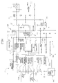
- an universal digital dimmer includes an electromagnetic radiation (EMR) control circuit 10, a zero level detector 20, a leading/trailing edge automatic detector 30, a encoded signal generator 40, a no-load detection circuit 50, a power supply circuit 60, a dual-core or multi-core microcontroller 70, a state indicator 80 and an output controller 713.
- the dual-core or multi-core microcontroller 70 is taken as a core and is connected to the zero level detector 20, the leading/trailing edge automatic detector 30, the encoded signal generator 40, the no-load detection circuit 50, the power supply circuit 60, the state indicator 80 and the output controller 713 respectively.
- the encoded signal generator 40 and the no-load detection circuit 50 are connected to each other.
- the EMR control circuit 10 is connected to an alternating current (AC) input at one end while the other end of the EMR control circuit 10 is connected to a rectifier circuit 11, a switch circuit 12, a low-power current amplifier and speed-up loop 13 and the output controller 713 in turn so that the output controller 713 can provide the AC power required to the load 1.
- the switch circuit 12 is further connected to a short-circuit protection circuit 14. One end of the short-circuit protection circuit 14 is to detect resistance in the switch circuit 12 while the other end thereof is connected to the output controller 713.
- partial current flows through the EMR control circuit 10 to the power supply circuit 60 so that the power supply circuit 60 can provide 5V direct current to the dual-core or multi-core microcontroller 70.
- the leading/trailing edge automatic detector 30 automatically switches the control mode to the leading edge control mode or the trailing edge control mode.
- the zero level detector 20 has the functionality of detecting waveform of the leading edge control mode and the trailing edge control mode so that the dimmer can work with inductive/capacitive/resistive load 1. Detection and automatic brightness/speed control are performed independently by respective dual-core or multi-core central processing unit (CPU) in the dual-core or multi-core microcontroller 70 so that the 0 ⁇ 100% dimming/speed control range of the load 1 is achieved.
- CPU central processing unit
- the dimmer is suitable for various kinds of load 1 and the brightness stability is improved.
- the EMR control circuit 10 consists of a noise harmonic suppression module and a high voltage impulse suppression module.
- the EMR control circuit 10 is further disposed with a X capacitor and a varisor/or transient voltage suppresser (TVS).
- the X capacitor is connected to the varisor/or TVS in parallel.
- the switching noise from the output controller 713 is suppressed by the EMR control circuit 10 so as to avoid interference to other equipment and protect the components in the dimmer free from outside interference. Also refer to Fig. 4 and Fig.
- the zero level detector 20 composed of a power waveform detection circuit and a zero crossing detection circuit is used for waveform detection of the leading edge control mode or of the trailing edge control mode.
- the zero level detector 20 mainly includes resistance R1, R2, R3 and a NPN transistor V.
- the resistance R1 and the resistance R2 are connected to a base b of the transistor V in parallel while an emitter e of the transistor V is grounded and a collector c of the transistor V is connected to the resistance R3.
- the resistance R3 is connected to a 5V power source. The intersection of the collector c of the transistor V and the resistance R3 is the zero point A of the detected input waveform.
- a signal of the zero point of the input waveform detected by the zero level detector 20 is sent to the dual-core or multi-core microcontroller 70.
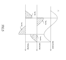
- the zero point is the point A in Fig. 4 and also refer to the waveform 1 in Fig. 6 .
- the waveform 2 in Fig. 6 it is an action waveform.
- the trailing edge control mode is used because that the start point is at the zero point and there is no switching noise.
- the LED light is a capacitive load 1 and the charging voltage is increased at a low speed. Thus no noise is generated in the whole dimming system. Yet if the LED light is an inductive load 1 (such as the waveform in Fig.
- the inductive load 1 will generate reverse voltage that damages the control component of the output controller 713 due to the flattened rising waveform and the steep off waveform in the trailing edge control mode. Thus a better performance is obtained while the leading edge control mode is selected.
- the signal of the point A in Fig. 4 is sent to the dual-core or multi-core microcontroller 70, with reference to the waveform 3 in Fig. 7 .
- the waveform 4 in Fig. 7 is an action waveform.
- the dual-core or multi-core microcontroller 70 is composed of a maximum value/minimum value setting circuit 701/702, an over-temperature protection circuit 703, an dimming up/down detection circuit704/705, a slow-start and memory module built in ON/OFF switch 706, an auto-hibernation circuit 707, an auto-wake-up circuit 708, a leading edge/trailing edge signal generator 709, a no-load detection circuit 710, a waveform abnormality detection circuit microcontroller 711, and an abnormal waveform detection, comparison and correction circuit 712.
- One end of the maximum value/minimum value setting circuit 701/702 is connected to the power supply circuit 60 and an adjustable resistance R4 is set therebetween while the other end of the maximum value/minimum value setting circuit 701/702 is connected to the output controller 713.
- One end of the over-temperature protection circuit 703 is connected to the no-load detection circuit 50 while the other end thereof is connected to the output controller 713.
- One end of the up/down detection circuit704/705 and one end of the slow-start and memory module built in ON/OFF switch 706 are connected to the encoded signal generator 40 respectively while the other end of the up/down detection circuit 704/705 is connected to the output controller 713.
- the slow-start and memory module built in ON/OFF switch 706, the auto-hibernation circuit 707, the auto-wake-up circuit 708, the leading edge/trailing edge signal generator 709, and the no-load detection circuit 710 are all connected to the output controller 713.
- One end of the waveform abnormality detection circuit microcontroller 711 is connected to the zero level detector 20 while the other end thereof is connected to the abnormal waveform detection, comparison and correction circuit 712.
- the abnormal waveform detection, comparison and correction circuit 712 is connected to the output controller 713.
- the maximum value/minimum value setting circuit 701/702 is used to set the maximum brightness/the minimum brightness.
- the minimum load is set by the minimum value setting circuit 702.
- the maximum value setting circuit 701 is used to set the maximum load, reduce the insertion loss of the dimmer, increase the power factor (PF) and avoid the flickering.
- the dual-core or multi-core microcontroller 70 is further disposed with a dimming DOF (depth of field) compensation circuit 714 so as to extend the original minimum load 20 ⁇ 40W to 3W required for startup.
- DOF depth of field
- the no-load detection circuit 710 sends signals to the output controller 713 under control of an encoder to realize the function of no-load detection and over-temperature detection with auto recovery.
- the short-circuit protection circuit 14 provides the dimmer a short-circuit protection (SCP) interface.
- SCP short-circuit protection
- a user interface of the dimmer can show the leading edge/trailing edge state due to the leading edge/trailing edge signal generator 709 while the output controller 713 is to control output energy.
- the state indicator 80 shows the current state of the dimming/speed.
- the auto-hibernation circuit 707 makes the dimmer enter hibernation automatically within the setting time while the dimmer resumes from hibernation by the auto-wake-up circuit 708.
- the encoded signal generator 40 includes a dimming-up switch 401, a dimming-down switch 402, and a push switch 403 used to control the on/off function.
- the dimming-up switch 401 is connected to the dimming up detection circuit 704 while the dimming-down switch 402 is connected to the dimming down detection circuit 705.
- the push switch 403 is connected to the slow-start and memory module built in ON/OFF switch 706. The ON/OFF function is performed through the encoded signal generator 40 and the last brightness level is stored in the encoded signal generator 40.
- the leading/trailing edge automatic detector 30 is connected to the dual-core or multi-core microcontroller 70 and having the following functions: (1) selecting and setting the leading edge control mode and the trailing edge control mode; (2) setting the minimum brightness and the maximum brightness; (3) setting the temperature protection.
- the encoded signal generator 40 is used for providing a user interface of the dimmer while the power supply circuit 60 provides power to the dual-core or multi-core microcontroller 70 and the output controller 713.
- the leading edge control mode or the trailing edge control mode is selected by the leading/trailing edge automatic detector 30 and the dimmer is switched to the leading edge or the trailing edge waveform.
- the dimmer can work with different loads 1.
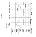
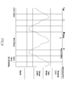
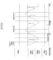
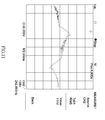
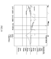
- the load 1 can be a capacitive load, an inductive load, or a resistive load that is selected from a halogen lamp, an electronic transformer, a compact fluorescent lamp ballast, a leading edge LED light, a trailing edge LED light, a fan speed controller etc. While in use, each different load 1 is connected to the dimmer in series and various waveforms are generated. For example, a waveform of the resistive load is shown in Fig. 8 . A waveform of capacitive load is shown in Fig. 9 . A waveform of inductive load is shown in Fig. 10 . As to Fig. 11 , it shows a waveform affected by load effect. The detection of the zero point A or charging/discharging of the load 1 will cause interference to the dimmer.
- the dual-core or multi-core microcontroller 70 is used to compare the power waveform with the dimming waveform to get distortion therebetween for correction of the waveform distortion. Thus smooth dimming and no flicker are achieved.
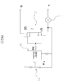
- the dual-core or multi-core microcontroller 70 is used for control in the present invention. As shown in Fig. 12 , the dual-core or multi-core microcontroller 70 is connected to the switch circuit 12 while the switch circuit 12 is formed by metal oxide semiconductor field effect transistor (MOSFET) Q1 and Q2 connected to each other in series. A resistance R5 is used to connect the switch circuit 12 and the dual-core or multi-core microcontroller 70.
- MOSFET metal oxide semiconductor field effect transistor
- the dual-core or multi-core microcontroller 70 When the MOSFET Q1 and the MOSFET Q2 are conducted, no signal is detected by the dual-core or multi-core microcontroller 70. Thus the prediction of how long a push signal is continuingly output is required at the next step before the MOSFET Q1 and the MOSFET Q2 are conducted. In each cycle, the frequency is corrected to 100HZ or 120HZ. The waveform distortion caused by load characteristics brings more loading to the detection and the operation. In the dual-core or multi-core microcontroller 70, one dual-core or multi-core central processing unit (CPU) is used for detection operation while the other/another dual-core or multi-core CPU is used for control operation.
- CPU central processing unit
- the preset waveform in the dual-core or multi-core microcontroller 70 is used as a baseline for correction.
- the detection starts with a lag of hundreds of microseconds ( ⁇ s) and this is beneficial to the signal detection.
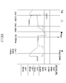
- Fig. 13 shows a standard waveform of the trigger signal (waveform 5) and a waveform of the output signal (waveform 6).
- Fig. 14 shows a waveform of the trigger signal (waveform 7) and a waveform with interference (waveform 8).
- the output signal reacts with a lag of 1ms (milli-second) behind the trigger signal.
- the rectifier circuit 11, the switch circuit 12, and the low-power current amplifier and speed-up loop 13 are disposed between the EMR control circuit 10 and the dual-core or multi-core microcontroller 70.
- the rectifier circuit 11 converts AC to direct current (DC) and provides DC to MOSFET Q1 and Q2 of the switch circuit 12 for switching on/off.
- signals output from the dual-core or multi-core microcontroller 70 pass through the low-power current amplifier and speed-up loop 13 to drive the MOSFET Q1 and Q2.
- Fig. 1 auto-correction of the maximum brightness and the minimum brightness is carried out at each time of on/off.
- the frequency of a counter inside the dual-core or multi-core microcontroller 70 is lowered to reduce the energy consumed.
- the dual-core or multi-core microcontroller 70 enters the sleep mode while detecting the light is off and automatically turns back to the operation mode automatically when the encoded signal generator 40 acts. Due to low current consumption in the system in which the dimmer and the load 1 are connected in series, the insertion loss is reduced and the maximum brightness is achieved. Moreover, the dual-core or multi-core microcontroller 70 enters hibernation within 2 seconds when the circuit is off so as to reduce loss.
- the state indicator 80 shows the current state of the dimmer while the output controller 713 is for control of output energy.
- the no-load detection circuit 50 transfers signals to the dual-core or multi-core microcontroller 70 under control of the encoded signal generator 40.
- the 0 ⁇ 100% brightness range of the load 1 (LED light) is divided into various levels under control of pulse width modulation (PWM). There are more levels at the low brightness level while fewer levels are provided at the high brightness level so as to compensate for changes in brightness levels. The minimum brightness level is set in order to turn on different loads 1 synchronously.
- PWM pulse width modulation
- the encoder is too sensitive when the on/off button is pressed and the speed control knob is rotated.
- the dimming function is set to be stopped when the on/off button is pressed. Once the on/off button is released, the dimming function is recovered and the light is dimmable by rotating the speed control knob.
- the dimmer includes the zero level detector to have the leading edge control mode and the trailing edge control mode. The dimmer detects and gets suitable waveform by switching between the leading edge control mode and the trailing edge control mode. Thus the dimmer can work well with different loads 1.
- detection and automatic dimming control are performed independently by the dual-core or multi-core microcontroller 70 so as to achieve 0 ⁇ 100% dimming range of the load 1.
- One dual-core or multi-core CPU of the dual-core or multi-core microcontroller 70 is used for detection operation while another dual-core or multi-core CPU is used for control operation.
- the dimmer is applicable to different loads 1 and the brightness stability is improved.
Landscapes
- Circuit Arrangement For Electric Light Sources In General (AREA)
- Discharge-Lamp Control Circuits And Pulse- Feed Circuits (AREA)
Applications Claiming Priority (1)
| Application Number | Priority Date | Filing Date | Title |
|---|---|---|---|
| CN201410231534.5A CN104035348B (zh) | 2014-05-29 | 2014-05-29 | 数位万用型调光器 |
Publications (3)
| Publication Number | Publication Date |
|---|---|
| EP2950620A2 true EP2950620A2 (de) | 2015-12-02 |
| EP2950620A3 EP2950620A3 (de) | 2016-02-24 |
| EP2950620B1 EP2950620B1 (de) | 2020-09-30 |
Family
ID=51466159
Family Applications (1)
| Application Number | Title | Priority Date | Filing Date |
|---|---|---|---|
| EP15167029.6A Not-in-force EP2950620B1 (de) | 2014-05-29 | 2015-05-08 | Universeller digitaler dimmer |
Country Status (4)
| Country | Link |
|---|---|
| EP (1) | EP2950620B1 (de) |
| CN (1) | CN104035348B (de) |
| AU (1) | AU2015100618A4 (de) |
| TW (1) | TWI634812B (de) |
Cited By (1)
| Publication number | Priority date | Publication date | Assignee | Title |
|---|---|---|---|---|
| CN115568076A (zh) * | 2022-08-26 | 2023-01-03 | 厦门天力源光电科技有限公司 | 一种兼容漏电保护电路的调光器控制方法 |
Families Citing this family (2)
| Publication number | Priority date | Publication date | Assignee | Title |
|---|---|---|---|---|
| CN104320875B (zh) * | 2014-10-13 | 2017-12-29 | 钟海停 | Led灯驱动电源高效节能专用模块 |
| CN109413797B (zh) * | 2018-10-22 | 2024-04-19 | 易光科技(江苏)有限公司 | 一种调节led电流曲线的控制电路 |
Family Cites Families (13)
| Publication number | Priority date | Publication date | Assignee | Title |
|---|---|---|---|---|
| US7259524B2 (en) * | 2004-06-10 | 2007-08-21 | Lutron Electronics Co., Inc. | Apparatus and methods for regulating delivery of electrical energy |
| DK1969691T3 (da) * | 2005-12-12 | 2012-07-23 | Clipsal Australia Pty Ltd | Belastningsdetektor til en dæmper |
| AU2008301235B2 (en) * | 2007-09-19 | 2012-11-15 | Clipsal Australia Pty Ltd | Dimmer circuit with overcurrent detection |
| KR101001241B1 (ko) * | 2008-09-05 | 2010-12-17 | 서울반도체 주식회사 | 교류 led 조광장치 및 그에 의한 조광방법 |
| US8242704B2 (en) * | 2008-09-09 | 2012-08-14 | Point Somee Limited Liability Company | Apparatus, method and system for providing power to solid state lighting |
| TWI401995B (zh) * | 2009-06-06 | 2013-07-11 | Anteya Technology Corp | Power switch switching dimmer and its LED device |
| CN101990331A (zh) * | 2009-08-07 | 2011-03-23 | 巨尔(上海)光电照明有限公司 | 一种基于led的triac调光方法 |
| US20120246650A1 (en) * | 2009-09-21 | 2012-09-27 | Bernd Mueller | Method for processing information and activities in a control and/or regulating system with the aid of a multi-core processor |
| ES2664198T3 (es) * | 2010-03-18 | 2018-04-18 | Philips Lighting Holding B.V. | Método y aparato para aumentar el rango de atenuación de dispositivos de iluminación de estado sólido |
| CN102939795B (zh) * | 2010-06-15 | 2016-11-09 | 马克西姆综合产品公司 | 可调光离线led驱动器 |
| CN201967196U (zh) * | 2010-12-08 | 2011-09-07 | 宁波科曼电子科技有限公司 | 一种电子式调光器 |
| AU2012297588B2 (en) * | 2011-11-03 | 2015-02-26 | Schneider Electric South East Asia (Hq) Pte Ltd | Dimmer arrangement |
| CN203930383U (zh) * | 2014-05-29 | 2014-11-05 | 东莞高仪电子科技有限公司 | 数位万用型调光器 |
-
2014
- 2014-05-29 CN CN201410231534.5A patent/CN104035348B/zh active Active
-
2015
- 2015-03-31 TW TW104110520A patent/TWI634812B/zh active
- 2015-05-08 AU AU2015100618A patent/AU2015100618A4/en not_active Expired
- 2015-05-08 EP EP15167029.6A patent/EP2950620B1/de not_active Not-in-force
Non-Patent Citations (1)
| Title |
|---|
| None |
Cited By (1)
| Publication number | Priority date | Publication date | Assignee | Title |
|---|---|---|---|---|
| CN115568076A (zh) * | 2022-08-26 | 2023-01-03 | 厦门天力源光电科技有限公司 | 一种兼容漏电保护电路的调光器控制方法 |
Also Published As
| Publication number | Publication date |
|---|---|
| TWI634812B (zh) | 2018-09-01 |
| EP2950620A3 (de) | 2016-02-24 |
| EP2950620B1 (de) | 2020-09-30 |
| CN104035348B (zh) | 2017-01-04 |
| AU2015100618A4 (en) | 2015-06-11 |
| CN104035348A (zh) | 2014-09-10 |
| TW201545601A (zh) | 2015-12-01 |
Similar Documents
| Publication | Publication Date | Title |
|---|---|---|
| US11316421B2 (en) | Apparatus, dimmable light emitting diode driver and control method | |
| US10652965B2 (en) | Apparatus, dimmable light emitting diode drive circuit and control method | |
| US11705807B2 (en) | Control circuit of power factor improvement circuit and semiconductor integrated circuit device | |
| US9271347B2 (en) | TRIAC dimmable LED driver circuit | |
| US9155138B2 (en) | Driver for cooperating with a wall dimmer | |
| US10021749B2 (en) | Phase control dimmer circuit with short-circuit protection | |
| US20130176004A1 (en) | Switching mode power supply | |
| EP3576497B1 (de) | Konstantspannungsgesteuerte dimmstromversorgung und dimmsystem für beleuchtungsvorrichtung | |
| US9408277B2 (en) | Control circuit for a phase-cut dimmer and a method of controlling a phase-cut dimmer | |
| JP6545946B2 (ja) | スイッチングコンバータおよびその制御回路、それを用いた照明装置、電子機器 | |
| AU2013262421B2 (en) | Method, apparatus and system for controlling an electrical load | |
| JP2008541372A (ja) | 汎用ライン電圧調光方法及びシステム | |
| JP5975774B2 (ja) | Led点灯装置 | |
| WO2015196672A1 (zh) | 功率因数校正电路自带辅助电源电路及其控制方法和装置 | |
| EP2950620B1 (de) | Universeller digitaler dimmer | |
| JP4349225B2 (ja) | 調光装置 | |
| EP2547172B1 (de) | Dimmer | |
| CN109379806B (zh) | 一种调光驱动电路、调光控制器和led灯具 | |
| US20230090441A1 (en) | Leakage protection circuit and dimming drive circuit | |
| JP6912136B1 (ja) | 調光装置 | |
| EP3349545B1 (de) | Beleuchtungssteuerungsvorrichtung | |
| CN203930383U (zh) | 数位万用型调光器 | |
| US9386641B2 (en) | Lighting dimmer synchronous load device | |
| KR101981155B1 (ko) | 입력 전류 레귤레이터, 그 구동 방법, 및 입력 전류 레귤레이터의 디스에이블회로 | |
| CN119300206A (zh) | 调光装置、用于控制调光装置的方法和存储介质 |
Legal Events
| Date | Code | Title | Description |
|---|---|---|---|
| AK | Designated contracting states |
Kind code of ref document: A2 Designated state(s): AL AT BE BG CH CY CZ DE DK EE ES FI FR GB GR HR HU IE IS IT LI LT LU LV MC MK MT NL NO PL PT RO RS SE SI SK SM TR |
|
| AX | Request for extension of the european patent |
Extension state: BA ME |
|
| PUAI | Public reference made under article 153(3) epc to a published international application that has entered the european phase |
Free format text: ORIGINAL CODE: 0009012 |
|
| PUAL | Search report despatched |
Free format text: ORIGINAL CODE: 0009013 |
|
| AK | Designated contracting states |
Kind code of ref document: A3 Designated state(s): AL AT BE BG CH CY CZ DE DK EE ES FI FR GB GR HR HU IE IS IT LI LT LU LV MC MK MT NL NO PL PT RO RS SE SI SK SM TR |
|
| AX | Request for extension of the european patent |
Extension state: BA ME |
|
| RIC1 | Information provided on ipc code assigned before grant |
Ipc: H05B 39/04 20060101AFI20160115BHEP |
|
| 17P | Request for examination filed |
Effective date: 20160805 |
|
| RBV | Designated contracting states (corrected) |
Designated state(s): AL AT BE BG CH CY CZ DE DK EE ES FI FR GB GR HR HU IE IS IT LI LT LU LV MC MK MT NL NO PL PT RO RS SE SI SK SM TR |
|
| STAA | Information on the status of an ep patent application or granted ep patent |
Free format text: STATUS: EXAMINATION IS IN PROGRESS |
|
| 17Q | First examination report despatched |
Effective date: 20170411 |
|
| GRAP | Despatch of communication of intention to grant a patent |
Free format text: ORIGINAL CODE: EPIDOSNIGR1 |
|
| STAA | Information on the status of an ep patent application or granted ep patent |
Free format text: STATUS: GRANT OF PATENT IS INTENDED |
|
| INTG | Intention to grant announced |
Effective date: 20200416 |
|
| GRAS | Grant fee paid |
Free format text: ORIGINAL CODE: EPIDOSNIGR3 |
|
| GRAA | (expected) grant |
Free format text: ORIGINAL CODE: 0009210 |
|
| STAA | Information on the status of an ep patent application or granted ep patent |
Free format text: STATUS: THE PATENT HAS BEEN GRANTED |
|
| AK | Designated contracting states |
Kind code of ref document: B1 Designated state(s): AL AT BE BG CH CY CZ DE DK EE ES FI FR GB GR HR HU IE IS IT LI LT LU LV MC MK MT NL NO PL PT RO RS SE SI SK SM TR |
|
| REG | Reference to a national code |
Ref country code: CH Ref legal event code: EP Ref country code: GB Ref legal event code: FG4D |
|
| REG | Reference to a national code |
Ref country code: AT Ref legal event code: REF Ref document number: 1320144 Country of ref document: AT Kind code of ref document: T Effective date: 20201015 |
|
| REG | Reference to a national code |
Ref country code: DE Ref legal event code: R096 Ref document number: 602015059731 Country of ref document: DE |
|
| REG | Reference to a national code |
Ref country code: IE Ref legal event code: FG4D |
|
| REG | Reference to a national code |
Ref country code: CH Ref legal event code: NV Representative=s name: LANGPATENT ANWALTSKANZLEI IP LAW FIRM, CH |
|
| REG | Reference to a national code |
Ref country code: NL Ref legal event code: FP |
|
| REG | Reference to a national code |
Ref country code: SE Ref legal event code: TRGR |
|
| PG25 | Lapsed in a contracting state [announced via postgrant information from national office to epo] |
Ref country code: FI Free format text: LAPSE BECAUSE OF FAILURE TO SUBMIT A TRANSLATION OF THE DESCRIPTION OR TO PAY THE FEE WITHIN THE PRESCRIBED TIME-LIMIT Effective date: 20200930 Ref country code: GR Free format text: LAPSE BECAUSE OF FAILURE TO SUBMIT A TRANSLATION OF THE DESCRIPTION OR TO PAY THE FEE WITHIN THE PRESCRIBED TIME-LIMIT Effective date: 20201231 Ref country code: BG Free format text: LAPSE BECAUSE OF FAILURE TO SUBMIT A TRANSLATION OF THE DESCRIPTION OR TO PAY THE FEE WITHIN THE PRESCRIBED TIME-LIMIT Effective date: 20201230 Ref country code: HR Free format text: LAPSE BECAUSE OF FAILURE TO SUBMIT A TRANSLATION OF THE DESCRIPTION OR TO PAY THE FEE WITHIN THE PRESCRIBED TIME-LIMIT Effective date: 20200930 |
|
| REG | Reference to a national code |
Ref country code: AT Ref legal event code: MK05 Ref document number: 1320144 Country of ref document: AT Kind code of ref document: T Effective date: 20200930 |
|
| REG | Reference to a national code |
Ref country code: NO Ref legal event code: T2 Effective date: 20200930 |
|
| PG25 | Lapsed in a contracting state [announced via postgrant information from national office to epo] |
Ref country code: RS Free format text: LAPSE BECAUSE OF FAILURE TO SUBMIT A TRANSLATION OF THE DESCRIPTION OR TO PAY THE FEE WITHIN THE PRESCRIBED TIME-LIMIT Effective date: 20200930 Ref country code: LV Free format text: LAPSE BECAUSE OF FAILURE TO SUBMIT A TRANSLATION OF THE DESCRIPTION OR TO PAY THE FEE WITHIN THE PRESCRIBED TIME-LIMIT Effective date: 20200930 |
|
| REG | Reference to a national code |
Ref country code: LT Ref legal event code: MG4D |
|
| PG25 | Lapsed in a contracting state [announced via postgrant information from national office to epo] |
Ref country code: CZ Free format text: LAPSE BECAUSE OF FAILURE TO SUBMIT A TRANSLATION OF THE DESCRIPTION OR TO PAY THE FEE WITHIN THE PRESCRIBED TIME-LIMIT Effective date: 20200930 Ref country code: RO Free format text: LAPSE BECAUSE OF FAILURE TO SUBMIT A TRANSLATION OF THE DESCRIPTION OR TO PAY THE FEE WITHIN THE PRESCRIBED TIME-LIMIT Effective date: 20200930 Ref country code: SM Free format text: LAPSE BECAUSE OF FAILURE TO SUBMIT A TRANSLATION OF THE DESCRIPTION OR TO PAY THE FEE WITHIN THE PRESCRIBED TIME-LIMIT Effective date: 20200930 Ref country code: EE Free format text: LAPSE BECAUSE OF FAILURE TO SUBMIT A TRANSLATION OF THE DESCRIPTION OR TO PAY THE FEE WITHIN THE PRESCRIBED TIME-LIMIT Effective date: 20200930 Ref country code: LT Free format text: LAPSE BECAUSE OF FAILURE TO SUBMIT A TRANSLATION OF THE DESCRIPTION OR TO PAY THE FEE WITHIN THE PRESCRIBED TIME-LIMIT Effective date: 20200930 Ref country code: PT Free format text: LAPSE BECAUSE OF FAILURE TO SUBMIT A TRANSLATION OF THE DESCRIPTION OR TO PAY THE FEE WITHIN THE PRESCRIBED TIME-LIMIT Effective date: 20210201 |
|
| PG25 | Lapsed in a contracting state [announced via postgrant information from national office to epo] |
Ref country code: ES Free format text: LAPSE BECAUSE OF FAILURE TO SUBMIT A TRANSLATION OF THE DESCRIPTION OR TO PAY THE FEE WITHIN THE PRESCRIBED TIME-LIMIT Effective date: 20200930 Ref country code: AT Free format text: LAPSE BECAUSE OF FAILURE TO SUBMIT A TRANSLATION OF THE DESCRIPTION OR TO PAY THE FEE WITHIN THE PRESCRIBED TIME-LIMIT Effective date: 20200930 Ref country code: AL Free format text: LAPSE BECAUSE OF FAILURE TO SUBMIT A TRANSLATION OF THE DESCRIPTION OR TO PAY THE FEE WITHIN THE PRESCRIBED TIME-LIMIT Effective date: 20200930 Ref country code: PL Free format text: LAPSE BECAUSE OF FAILURE TO SUBMIT A TRANSLATION OF THE DESCRIPTION OR TO PAY THE FEE WITHIN THE PRESCRIBED TIME-LIMIT Effective date: 20200930 Ref country code: IS Free format text: LAPSE BECAUSE OF FAILURE TO SUBMIT A TRANSLATION OF THE DESCRIPTION OR TO PAY THE FEE WITHIN THE PRESCRIBED TIME-LIMIT Effective date: 20210130 |
|
| PG25 | Lapsed in a contracting state [announced via postgrant information from national office to epo] |
Ref country code: SK Free format text: LAPSE BECAUSE OF FAILURE TO SUBMIT A TRANSLATION OF THE DESCRIPTION OR TO PAY THE FEE WITHIN THE PRESCRIBED TIME-LIMIT Effective date: 20200930 |
|
| REG | Reference to a national code |
Ref country code: DE Ref legal event code: R097 Ref document number: 602015059731 Country of ref document: DE |
|
| PLBE | No opposition filed within time limit |
Free format text: ORIGINAL CODE: 0009261 |
|
| STAA | Information on the status of an ep patent application or granted ep patent |
Free format text: STATUS: NO OPPOSITION FILED WITHIN TIME LIMIT |
|
| PG25 | Lapsed in a contracting state [announced via postgrant information from national office to epo] |
Ref country code: DK Free format text: LAPSE BECAUSE OF FAILURE TO SUBMIT A TRANSLATION OF THE DESCRIPTION OR TO PAY THE FEE WITHIN THE PRESCRIBED TIME-LIMIT Effective date: 20200930 |
|
| 26N | No opposition filed |
Effective date: 20210701 |
|
| PG25 | Lapsed in a contracting state [announced via postgrant information from national office to epo] |
Ref country code: SI Free format text: LAPSE BECAUSE OF FAILURE TO SUBMIT A TRANSLATION OF THE DESCRIPTION OR TO PAY THE FEE WITHIN THE PRESCRIBED TIME-LIMIT Effective date: 20200930 |
|
| REG | Reference to a national code |
Ref country code: DE Ref legal event code: R119 Ref document number: 602015059731 Country of ref document: DE |
|
| REG | Reference to a national code |
Ref country code: SE Ref legal event code: EUG |
|
| REG | Reference to a national code |
Ref country code: CH Ref legal event code: PL |
|
| REG | Reference to a national code |
Ref country code: NL Ref legal event code: MM Effective date: 20210601 |
|
| GBPC | Gb: european patent ceased through non-payment of renewal fee |
Effective date: 20210508 |
|
| PG25 | Lapsed in a contracting state [announced via postgrant information from national office to epo] |
Ref country code: SE Free format text: LAPSE BECAUSE OF NON-PAYMENT OF DUE FEES Effective date: 20210509 Ref country code: LU Free format text: LAPSE BECAUSE OF NON-PAYMENT OF DUE FEES Effective date: 20210508 Ref country code: MC Free format text: LAPSE BECAUSE OF FAILURE TO SUBMIT A TRANSLATION OF THE DESCRIPTION OR TO PAY THE FEE WITHIN THE PRESCRIBED TIME-LIMIT Effective date: 20200930 Ref country code: LI Free format text: LAPSE BECAUSE OF NON-PAYMENT OF DUE FEES Effective date: 20210531 Ref country code: CH Free format text: LAPSE BECAUSE OF NON-PAYMENT OF DUE FEES Effective date: 20210531 |
|
| REG | Reference to a national code |
Ref country code: BE Ref legal event code: MM Effective date: 20210531 |
|
| PG25 | Lapsed in a contracting state [announced via postgrant information from national office to epo] |
Ref country code: IE Free format text: LAPSE BECAUSE OF NON-PAYMENT OF DUE FEES Effective date: 20210508 Ref country code: GB Free format text: LAPSE BECAUSE OF NON-PAYMENT OF DUE FEES Effective date: 20210508 Ref country code: DE Free format text: LAPSE BECAUSE OF NON-PAYMENT OF DUE FEES Effective date: 20211201 |
|
| PG25 | Lapsed in a contracting state [announced via postgrant information from national office to epo] |
Ref country code: IS Free format text: LAPSE BECAUSE OF FAILURE TO SUBMIT A TRANSLATION OF THE DESCRIPTION OR TO PAY THE FEE WITHIN THE PRESCRIBED TIME-LIMIT Effective date: 20210130 Ref country code: NL Free format text: LAPSE BECAUSE OF NON-PAYMENT OF DUE FEES Effective date: 20210601 Ref country code: FR Free format text: LAPSE BECAUSE OF NON-PAYMENT OF DUE FEES Effective date: 20210531 |
|
| PG25 | Lapsed in a contracting state [announced via postgrant information from national office to epo] |
Ref country code: BE Free format text: LAPSE BECAUSE OF NON-PAYMENT OF DUE FEES Effective date: 20210531 |
|
| PG25 | Lapsed in a contracting state [announced via postgrant information from national office to epo] |
Ref country code: IT Free format text: LAPSE BECAUSE OF NON-PAYMENT OF DUE FEES Effective date: 20210508 |
|
| PG25 | Lapsed in a contracting state [announced via postgrant information from national office to epo] |
Ref country code: HU Free format text: LAPSE BECAUSE OF FAILURE TO SUBMIT A TRANSLATION OF THE DESCRIPTION OR TO PAY THE FEE WITHIN THE PRESCRIBED TIME-LIMIT; INVALID AB INITIO Effective date: 20150508 |
|
| PG25 | Lapsed in a contracting state [announced via postgrant information from national office to epo] |
Ref country code: CY Free format text: LAPSE BECAUSE OF FAILURE TO SUBMIT A TRANSLATION OF THE DESCRIPTION OR TO PAY THE FEE WITHIN THE PRESCRIBED TIME-LIMIT Effective date: 20200930 |
|
| PG25 | Lapsed in a contracting state [announced via postgrant information from national office to epo] |
Ref country code: MK Free format text: LAPSE BECAUSE OF FAILURE TO SUBMIT A TRANSLATION OF THE DESCRIPTION OR TO PAY THE FEE WITHIN THE PRESCRIBED TIME-LIMIT Effective date: 20200930 |
|
| PGFP | Annual fee paid to national office [announced via postgrant information from national office to epo] |
Ref country code: NO Payment date: 20240618 Year of fee payment: 10 |
|
| PG25 | Lapsed in a contracting state [announced via postgrant information from national office to epo] |
Ref country code: MT Free format text: LAPSE BECAUSE OF FAILURE TO SUBMIT A TRANSLATION OF THE DESCRIPTION OR TO PAY THE FEE WITHIN THE PRESCRIBED TIME-LIMIT Effective date: 20200930 |
|
| PG25 | Lapsed in a contracting state [announced via postgrant information from national office to epo] |
Ref country code: TR Free format text: LAPSE BECAUSE OF FAILURE TO SUBMIT A TRANSLATION OF THE DESCRIPTION OR TO PAY THE FEE WITHIN THE PRESCRIBED TIME-LIMIT Effective date: 20200930 |
|
| PG25 | Lapsed in a contracting state [announced via postgrant information from national office to epo] |
Ref country code: NO Free format text: LAPSE BECAUSE OF NON-PAYMENT OF DUE FEES Effective date: 20250531 |