EP2952060B1 - Circuit électrique et procédé pour faire fonctionner et varier au moins une led - Google Patents
Circuit électrique et procédé pour faire fonctionner et varier au moins une led Download PDFInfo
- Publication number
- EP2952060B1 EP2952060B1 EP13811533.2A EP13811533A EP2952060B1 EP 2952060 B1 EP2952060 B1 EP 2952060B1 EP 13811533 A EP13811533 A EP 13811533A EP 2952060 B1 EP2952060 B1 EP 2952060B1
- Authority
- EP
- European Patent Office
- Prior art keywords
- dimming
- circuit
- coupled
- output
- frequency
- Prior art date
- Legal status (The legal status is an assumption and is not a legal conclusion. Google has not performed a legal analysis and makes no representation as to the accuracy of the status listed.)
- Active
Links
- 238000000034 method Methods 0.000 title claims description 10
- 239000003990 capacitor Substances 0.000 claims description 13
- 230000008878 coupling Effects 0.000 claims description 13
- 238000010168 coupling process Methods 0.000 claims description 13
- 238000005859 coupling reaction Methods 0.000 claims description 13
- 230000000875 corresponding effect Effects 0.000 claims description 7
- 230000003247 decreasing effect Effects 0.000 claims description 5
- 238000005259 measurement Methods 0.000 claims description 3
- 230000002596 correlated effect Effects 0.000 claims description 2
- 230000000873 masking effect Effects 0.000 claims 1
- 230000006735 deficit Effects 0.000 description 5
- 241000282414 Homo sapiens Species 0.000 description 4
- 230000000694 effects Effects 0.000 description 2
- 238000002955 isolation Methods 0.000 description 2
- 230000001105 regulatory effect Effects 0.000 description 2
- 241000282412 Homo Species 0.000 description 1
- 230000004913 activation Effects 0.000 description 1
- 230000002411 adverse Effects 0.000 description 1
- 230000000295 complement effect Effects 0.000 description 1
- 230000003467 diminishing effect Effects 0.000 description 1
- 230000004907 flux Effects 0.000 description 1
- 238000011835 investigation Methods 0.000 description 1
- 230000004048 modification Effects 0.000 description 1
- 238000012986 modification Methods 0.000 description 1
- 230000010355 oscillation Effects 0.000 description 1
- 230000000737 periodic effect Effects 0.000 description 1
- 230000002265 prevention Effects 0.000 description 1
- 230000009467 reduction Effects 0.000 description 1
- 238000009877 rendering Methods 0.000 description 1
- 230000002441 reversible effect Effects 0.000 description 1
- 238000012549 training Methods 0.000 description 1
- 238000011144 upstream manufacturing Methods 0.000 description 1
- 238000004804 winding Methods 0.000 description 1
Images


Classifications
-
- H—ELECTRICITY
- H05—ELECTRIC TECHNIQUES NOT OTHERWISE PROVIDED FOR
- H05B—ELECTRIC HEATING; ELECTRIC LIGHT SOURCES NOT OTHERWISE PROVIDED FOR; CIRCUIT ARRANGEMENTS FOR ELECTRIC LIGHT SOURCES, IN GENERAL
- H05B45/00—Circuit arrangements for operating light-emitting diodes [LED]
- H05B45/30—Driver circuits
- H05B45/37—Converter circuits
- H05B45/3725—Switched mode power supply [SMPS]
- H05B45/382—Switched mode power supply [SMPS] with galvanic isolation between input and output
-
- H—ELECTRICITY
- H05—ELECTRIC TECHNIQUES NOT OTHERWISE PROVIDED FOR
- H05B—ELECTRIC HEATING; ELECTRIC LIGHT SOURCES NOT OTHERWISE PROVIDED FOR; CIRCUIT ARRANGEMENTS FOR ELECTRIC LIGHT SOURCES, IN GENERAL
- H05B45/00—Circuit arrangements for operating light-emitting diodes [LED]
- H05B45/10—Controlling the intensity of the light
-
- H—ELECTRICITY
- H05—ELECTRIC TECHNIQUES NOT OTHERWISE PROVIDED FOR
- H05B—ELECTRIC HEATING; ELECTRIC LIGHT SOURCES NOT OTHERWISE PROVIDED FOR; CIRCUIT ARRANGEMENTS FOR ELECTRIC LIGHT SOURCES, IN GENERAL
- H05B45/00—Circuit arrangements for operating light-emitting diodes [LED]
- H05B45/30—Driver circuits
- H05B45/37—Converter circuits
- H05B45/3725—Switched mode power supply [SMPS]
- H05B45/39—Circuits containing inverter bridges
-
- Y—GENERAL TAGGING OF NEW TECHNOLOGICAL DEVELOPMENTS; GENERAL TAGGING OF CROSS-SECTIONAL TECHNOLOGIES SPANNING OVER SEVERAL SECTIONS OF THE IPC; TECHNICAL SUBJECTS COVERED BY FORMER USPC CROSS-REFERENCE ART COLLECTIONS [XRACs] AND DIGESTS
- Y02—TECHNOLOGIES OR APPLICATIONS FOR MITIGATION OR ADAPTATION AGAINST CLIMATE CHANGE
- Y02B—CLIMATE CHANGE MITIGATION TECHNOLOGIES RELATED TO BUILDINGS, e.g. HOUSING, HOUSE APPLIANCES OR RELATED END-USER APPLICATIONS
- Y02B20/00—Energy efficient lighting technologies, e.g. halogen lamps or gas discharge lamps
- Y02B20/30—Semiconductor lamps, e.g. solid state lamps [SSL] light emitting diodes [LED] or organic LED [OLED]
Definitions
- the present invention relates to a circuit arrangement for operating and dimming at least one LED comprising an input having a first and a second input terminal for coupling to a DC supply voltage, at least a first and a second electronic switch in bridge arrangement, wherein the first and the second electronic switch under training a bridge center are serially coupled between the first and second input terminals, an output having first and second output terminals for connecting the at least one LED, a choke, a rectifier having a rectifier input and a rectifier output, the choke between the bridge center and the rectifier input is coupled, wherein the rectifier output is coupled to the output of the circuit arrangement, and a drive device having at least a first and a second output for supplying drive signals n to the first and the second electronic switch, wherein the drive signals have a predetermined frequency, wherein the drive device has an input for supplying dimming information, wherein the drive device is designed to increase the frequency of the drive signals for dimming the at least one LED with increasing dimming , It also relates to a
- the present invention relates to the problem that LEDs are to be operated and dimmed inexpensively in a simple manner, without causing audible or visible impairments, such as a humming or Flickererscheinept.
- a generic circuit arrangement for operating at least one LED and a method for their operation discloses the DE 10 2005 058 484 A1 ,
- pulse width modulation frequencies of a few 100 Hz are used. Although these are not consciously perceived by the human eye, they can lead to stroboscopic and thus disturbing effects. In addition, the low frequencies are in the human hearing range and can thus lead to unwanted noise nuisance.
- a circuit arrangement with a downstream pulse width modulation for further dimming of LEDs discloses the US 2012/0181940 A1 , Here, during a first dimming range, the converter frequency is increased to decrease the current through the LEDs, and in a second range this dimming is combined with a superimposed PWM dimming.
- the object of the present invention is therefore to develop a generic circuit arrangement or an initially mentioned method such that the operation and dimming of LEDs at greatly reduced visible or audible interference is enabled.
- the present invention is based on the finding that in a generic circuit arrangement by increasing the frequency while a dimming can be achieved, however, occur with increasing dimming above a certain threshold shifts of the color location, which in turn can be perceived by the human eye and thus undesirable visible disturbances to lead.
- the invention is therefore the way to increase the dimming of the at least one LED, the frequency of the drive signals with increasing dimming only up to a predefinable dimming threshold. If it is to be further decreased, ie, that even less light is to be emitted, the invention switches to a different procedure:
- the circuit arrangement further comprises a short-circuit device having at least one input and at least one output, wherein the at least one input of the short-circuit device with at least one Output of the drive device is coupled, wherein the at least one output of the short-circuiting device is coupled to the rectifier input, wherein the drive device is further configured to set a dimming value, which is below the predetermined dimming threshold, to activate the short-circuiting device during predeterminable periods.
- the nomenclature of the present application refers to an increasing Dimming a diminishing dimming value and thus a decrease in the emitted light.
- a generic circuit arrangement is known in principle from electronic ballasts for fluorescent lamps, in particular low-pressure fluorescent lamps.
- the frequency is increased in the upper dimming range, ie from approx. 100% to 20 to 30% light, thus reducing the LED current.
- the frequencies are typically above 40 kHz and therefore are not audible.
- the frequency of the bridge arrangement is raised. The increase in frequency reduces the current supplied to the LEDs and thus reduces the emitted light.
- the dithering bridge frequency is kept at values below 20 to 30% constant at the high level of the dimming threshold required to set the LED current to 20 to 30%.
- the frequency of the bridge arrangement is in this case at about 150 to 200 kHz, well above the audible range.
- the luminous flux of the LEDs is now further reduced by a high-frequency hiding individual of the high-frequency current half-waves.
- the fade out frequency is greater than 20 kHz and is therefore higher than the audible range, but much smaller than the bridge frequency. By doing so, the LED peak current level remains constant, so color reproduction is not affected.
- Different degrees of dimming can be set by cutting one to several half waves per unit time. This procedure allows dimming to 0% light. All frequencies are above the audible frequency for humans. Shades of the dimmed light can be achieved by varying the number of current half-waves cut out between individual cycles according to a predeterminable scheme.
- the frequency of the drive signals for setting a dimming value which corresponds to the dimming threshold value, a frequency maximum value.
- the drive device is furthermore preferably designed to set the frequency drive signals to the maximum frequency value for setting a dimming value which is below the predefinable dimming threshold value. Dimming values up to 0% are thus possible without acoustic or visible impairments.
- the short-circuit device preferably comprises at least one series circuit of an electronic switch and at least one diode, wherein the input of the electroni coupled switch with the other output of the drive device, wherein the series circuit between the output of the short-circuiting device and a reference potential is coupled.
- the short-circuit device can be controlled in a suitable manner to hide predeterminable half-waves of the bridge current.
- the short-circuit device comprises a first series circuit comprising a first electronic switch and a first diode and a second series circuit comprising a second electronic switch and a second diode, wherein the first and the second series circuit are connected in parallel, wherein the first diode and the second diode are arranged with different orientation.
- the short-circuit device comes with only an electronic switch. It includes a first, a second, a third and a fourth diode.
- the first and second diodes are coupled in series between the output of the shorting device and the reference potential to form a first coupling point with mutually oriented cathodes, while the third and fourth diodes couple in series between the output of the second anode to form a second coupling point with mutually-oriented anodes Shorting device and the reference potential are coupled.
- the working electrode of the electronic switch is connected to the first coupling point and the reference electrode of the electronic switch coupled to the second coupling point.
- a transformer may be coupled between the choke and the rectifier to provide galvanic isolation between the input and the output of the circuitry.
- the circuit arrangement comprises a current measuring device, in particular a shunt resistor, which is designed to measure a current that is correlated with the current through the at least one LED, the current measuring device for regulating the current through the at least one LED the drive device is coupled.
- a current measuring device in particular a shunt resistor, which is designed to measure a current that is correlated with the current through the at least one LED, the current measuring device for regulating the current through the at least one LED the drive device is coupled.
- the circuit arrangement further comprises a link capacitor coupled between the first and second input terminals.
- the circuitry may further include a bridge capacitor coupled between the inductor and the rectifier.
- a resonance capacitor can be provided which is coupled between the connection of the throttle, which is not coupled to the bridge center, and the reference potential.
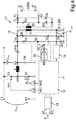
- Fig. 1 shows a schematic representation of a first embodiment of a circuit arrangement according to the invention. This has an input with a first E1 and a second input terminal E2 for coupling to a DC supply voltage, which in the present case represents the so-called intermediate circuit voltage U Zw .
- a DC supply voltage which in the present case represents the so-called intermediate circuit voltage U Zw .
- This is preferably generated by an upstream PFC controller from an AC line voltage, regulated and is usually of the order of 400 V DC.
- an intermediate circuit capacitor C Zw is coupled to buffer the intermediate circuit voltage U Zw .
- the circuit arrangement further comprises a first Q1 and a second transistor Q2 in a half-bridge arrangement, wherein the two transistors Q1, Q2 are coupled in series between the first and the second input terminal E1, E2 to form a half-bridge center HB.
- the present invention could also be realized with a full bridge.
- the circuit arrangement furthermore comprises an output with a first and a second output connection A1, A2 for connecting at least one LED.
- a half-bridge center HB and the first output terminal A1 the series circuit of a choke L, a half-bridge capacitor CHB and a rectifier 10 is coupled, the latter comprising the diodes D1, D2, D3 and D4. Since the resistance of the inductor L increases with increasing frequency, the current I CHB for dimming the LEDs can be reduced by increasing the frequency.
- a drive device 12 is designed to drive the transistor Q1 via a first output HA1 and the transistor Q2 via a second output HA2.
- a high-side driver HD which additionally serves as levelshifter coupled, while between the output HA2 and the control electrode of the transistor Q2, a low-side driver LD is coupled.
- the drive device 12 is coupled to an interface 14, via whose inputs SE1, SE2 the drive device 12, a dimming information D I can be fed.
- the interface 14 can in particular represent a DALI interface or a so-called 1-10 volt interface.
- a shunt resistor R ILED is coupled between the rectifier 10 and the reference potential, the voltage U ILED dropping across the resistor R ILED being coupled to the drive device 12 via a matching circuit 16.
- the matching circuit 16 is designed to generate from the voltage U ILED a measurement signal which is proportional to the current through the LEDs and which can be processed by the drive device 12.
- the drive device 12 is preferably designed as a microcontroller.
- the capacitor CHB current flowing through I CHB is an alternating current, which means it is made up of positive and negative half cycles.
- the drive signals AH, AL for the transistors Q1, Q2 are square wave signals at a variable frequency f HB .
- the drive device 12 is now designed to increase Dimming, that is, with increasing reduction of the light to be emitted by the LEDs to increase the frequency f HB up to a predetermined threshold SW.
- the frequency f HBmax at the threshold SW represents a maximum frequency value, which is not exceeded according to the invention.
- the threshold value SW is preferably between 20 and 30% of the maximum light that can be emitted by the LEDs.
- the frequency f HB is in the undimmed state at, for example, 40 kHz.
- the frequency f HBmax at the dimming threshold SW is for example between 150 and 200 kHz.
- the circuit arrangement has a first series circuit comprising a diode D5 and a transistor Q3 and a second series circuit coupled thereto in parallel, which comprises a diode D6 and a transistor Q4.
- the diodes D5 and D6 are oriented differently, while the transistors Q3 and Q4 are made complementary.
- the drive device 12 has two further outputs, namely an output AB1, which is coupled via a driver PD to the control electrode of the transistor Q4, and an output AB2, which is coupled via a driver ND to the control electrode of the transistor Q3.
- the series circuits D5 and Q3 on the one hand and D6 and Q4 on the other hand form a short-circuit device 18.
- the transistor Q3 is turned on by means of the output signal AB2, the corresponding half-wave is short-circuited and therefore absent in the input signal of the rectifier 10. Because the diode D6 is oriented opposite to the diode D5, the series connection of the diode D6 and the transistor Q4 does not affect this phase. If, conversely, at a time when the current I CHB has a negative half-wave, the transistor Q4 is turned on by means of the output signal AB1, the negative half-cycle is short-circuited and is absent in the output signal provided to the rectifier 10. The series connection of the diode D5 and the transistor Q3 then does not affect this phase.
- the transistors Q3 and Q4 are driven with a signal having a frequency of 20 kHz. This frequency is above the audible range and therefore does not cause any acoustic interference.
- dimming for example, instead of blanking every tenth half-wave, for example, n consecutive half-waves can be short-circuited, where n is between 1 and 10. As will be apparent to those skilled in the art, by shorting every nth half-wave, the degree of dimming can also be varied.
- Fig. 1 Particularly advantageous at the in Fig. 1
- the embodiment shown is the circumstance that an activation of the switches Q3, Q4 with respect to internal ground is possible. This makes the drivers PD and ND particularly easy and inexpensive to implement. Also advantageous is that the switches Q3, Q4 can always be switched in the de-energized state, that is, when the associated diode is in the reverse direction. This makes the control simple and time-critical. This results in a particularly low power loss and in the prevention of EMC interference.
- Fig. 2 illustrated embodiment differs from the in Fig. 1 represented by the fact that the output circuit is galvanically isolated from the input circuit by using a transformer Tr.
- a series circuit which comprises the primary inductance PI and the shunt resistor R ILED is coupled in parallel with the series circuits D5 and Q3 on the one hand and D6 and Q4 on the other hand.
- the secondary inductance SI is coupled to the input of the rectifier 10.
- a transformer Tr If a transformer Tr is used, care must be taken to alternately short-circuit positive and negative half-waves so that the transformer does not saturate. In other words this means that the mean value of the integral of the current of the primary winding PI must be zero. Accordingly, both series circuits, ie Q3 and D5 on the one hand and Q4 and D6 on the other hand, should be provided.
- Fig. 3 illustrated embodiment is compared to the in Fig. 1 illustrated embodiment for short-circuiting half-waves of the current I CHB only one switch provided, namely the switch Q3.
- the diode D7 is antiserially coupled to the diode D5, while the diode D8 is antiserially coupled to the diode D6.
- the coupling point of the diode D5 with the diode D7 is denoted by N2
- the coupling point of the diode D6 with the diode D8 is denoted by N3.
- the control electrode of the switch Q3 is coupled via a driver 20 to the output AB of the driver 12, the working or reference electrode of the switch Q3 is coupled to the node N2 and the node N3, respectively.
- the driver 20 also serves as a level shifter for the switch Q3.
- the level shifter is necessary because the switch terminals vary in potential. Compared to the embodiments according to Fig. 1 and Fig. 2 is for the embodiment according to Fig. 3 to generate the drive signal more complex and accurate, since the switch Q3 should only be turned on when the capacitor CR is just discharged. Otherwise, switching losses and increased radio interference would arise. However, as stated, a switch can be saved.
- Fig. 4 shows a modification of the embodiment of Fig. 3 , again with a transformer Tr, cf. Fig. 2 , is used for galvanic isolation of input and output circuit. It is again important to ensure that alternating positive and negative half-waves are excluded in order to avoid saturation of the primary inductance PI.
Landscapes
- Circuit Arrangement For Electric Light Sources In General (AREA)
Claims (10)
- Circuit électrique pour faire fonctionner et varier au moins une DEL, comprenant :- une entrée avec une première (E1) et une deuxième borne d'entrée (E2) pour couplage à une tension continue d'alimentation (Uzw);- au moins un premier (Q1) et un deuxième commutateur électronique (Q2) montés en pont, le premier (Q1) et le deuxième commutateur électronique (Q2) étant couplés en série entre la première (E1) et la deuxième borne d'entrée (E2) avec formation d'un point central de pont (HB);- une sortie avec une première (A1) et une deuxième borne de sortie (A2) pour connecter l'au moins une DEL ;- une self (L) ;- un redresseur (10) avec une entrée de redresseur et une sortie de redresseur, la self (L) étant couplée entre le point central de pont (HB) et l'entrée de redresseur, la sortie de redresseur étant couplée à la sortie (A1, A2) du circuit ; et- un dispositif de commande (12) avec au moins une première (HA1) et une deuxième sortie (HA2) pour amener des signaux de commande correspondants (AH, AL) au premier (Q1) et au deuxième commutateur électronique (Q2), les signaux de commande (AH, AL) présentant une fréquence prédéterminable (fHB), le dispositif de commande (12) comportant une entrée (SE1, SE2) pour amener une information de variation (DI), le dispositif de commande (12) étant conçu pour augmenter la fréquence (fHB) des signaux de commande (AH, AL) pour faire varier l'au moins une DEL dans le cas d'une variation croissante, une variation croissante désignant une valeur de variation décroissante et donc une diminution de la lumière émise ;
caractérisé en ce que
le dispositif de commande (12) est conçu pour augmenter la fréquence (fHB) des signaux de commande correspondants (AH, AL), pour faire varier l'au moins une DEL, jusqu'à ce que la valeur de variation décroissante atteigne une valeur seuil de variation prédéterminable (SW), la fréquence (fHB) des signaux de commande (AH, AL) pour le réglage de la valeur de variation qui correspond à la valeur seuil de variation (SW) représentant une valeur maximale de fréquence (fHBmax),
le circuit comprenant en outre un dispositif de court-circuit (18) pour occulter un signal de sortie du montage en pont pendant des laps de temps prédéterminables avec au moins une entrée et au moins une sortie,
l'au moins une entrée du dispositif de court-circuit (18) étant couplée à au moins une autre sortie (AB1, AB2 ; AB) du dispositif de commande (12),
l'au moins une sortie du dispositif de court-circuit (18) étant couplée à l'entrée de redresseur,
le dispositif de commande (12) étant en outre conçu pour régler, afin de régler une quelconque valeur de variation qui est inférieure à la valeur seuil de variation prédéterminable (SW), la fréquence des signaux de commande sur la valeur maximale de fréquence et activer le dispositif de court-circuit (18) pendant les laps de temps prédéterminables,
et les laps de temps prédéterminables correspondant à un multiple entier de demi-ondes distinctes du signal de sortie du montage en pont. - Circuit selon la revendication 1, caractérisé en ce que le dispositif de court-circuit (18) comprend au moins un montage en série, un commutateur électronique (Q3, Q4) et au moins une diode (D5, D6, D7, D8), l'entrée du commutateur électronique étant couplée à l'autre sortie (AB) du dispositif de commande (12), l'au moins un montage en série étant couplé entre la sortie du dispositif de court-circuit (18) et un potentiel de référence.
- Circuit selon la revendication 2, caractérisé en ce que le dispositif de court-circuit (18), complémentairement au premier de l'au moins un montage en série comprenant le premier commutateur électronique (Q3) et la première diode (D5), comprend un deuxième de l'au moins un montage en série comprenant le deuxième commutateur électronique(Q4) et la deuxième diode (D6), le premier (Q3, D5) et le deuxième montage en série (Q4, D6) étant montés en parallèle, la première diode (D5) et la deuxième diode (D6) étant agencées avec une orientation différente.
- Circuit selon la revendication 2, caractérisé en ce que le dispositif de court-circuit (18), complémentairement au commutateur électronique (Q3, Q4) et à la première diode (D5), comprend une deuxième (D7), une troisième (D6) et une quatrième diode (D8),
la première et la deuxième diode étant couplées en formant un premier point de couplage avec des cathodes orientées l'une vers l'autre en série entre la sortie du dispositif de court-circuit (18) et le potentiel de référence,
la troisième et la quatrième diode étant couplées en formant un deuxième point de couplage avec des anodes orientées l'une vers l'autre en série entre la sortie du dispositif de court-circuit (18) et le potentiel de référence,
l'électrode de travail du commutateur électronique (Q3, Q4) étant couplée au premier point de couplage et l'électrode de référence du commutateur électronique (Q3, Q4), au deuxième point de couplage. - Circuit selon l'une des revendications précédentes, caractérisé en ce que le circuit comprend en outre un transformateur (Tr) qui est couplé entre la self (L) et le redresseur (10).
- Circuit selon l'une des revendications précédentes, caractérisé en ce qu'il comprend un dispositif de mesure de courant (RILED), et plus particulièrement une résistance de shunt, qui est conçu pour mesurer un courant qui est corrélé avec le courant passant par l'au moins une DEL, le dispositif de mesure de courant (RILED) étant, pour le réglage du courant passant par l'au moins une DEL, couplé au dispositif de commande (12).
- Circuit selon l'une des revendications précédentes, caractérisé en ce que le circuit comprend en outre un condensateur de circuit intermédiaire (CZw) qui est couplé entre la première (E1) et la deuxième borne d'entrée (E2).
- Circuit selon l'une des revendications précédentes, caractérisé en ce que le circuit comprend en outre un condensateur en pont (CHB) qui est couplé entre la self (L) et le redresseur (10).
- Circuit selon l'une des revendications précédentes, caractérisé en ce que le circuit comprend en outre un condensateur de résonance (CR) qui est couplé entre la borne de la self (L) non couplée au point central de pont (HB) et le potentiel de référence.
- Procédé pour faire fonctionner et varier au moins une DEL au moyen d'un circuit selon la revendication 1, des signaux de commande correspondants (AH, AL) étant amenés avec une fréquence prédéterminable (fHB) au premier et au deuxième commutateur électronique au moyen du dispositif de commande (12), une information de variation (DI) étant amenée au dispositif de commande (12) via une entrée (SE1, SE2), la fréquence (fHB) des signaux de commande (AH, AL) étant augmentée au moyen du dispositif de commande (12) pour faire varier l'au moins une DEL dans le cas d'une variation croissante, une variation croissante désignant une valeur de variation décroissante, et donc une diminution de la lumière émise,
caractérisé en ce que,
pour faire varier l'au moins une DEL, la fréquence (fHB) des signaux de commande correspondants (AH, AL) est augmentée jusqu'à ce que la valeur de variation décroissante atteigne une valeur seuil de variation prédéterminable (SW), la fréquence (fHB) des signaux de commande (AH, AL) pour le réglage de la valeur de variation qui correspond à la valeur seuil de variation (SW) représentant une valeur maximale de fréquence (fHBmax) et,
pour le réglage d'une quelconque valeur de variation qui est inférieure à la valeur seuil de variation prédéterminable (SW), la fréquence des signaux de commande étant réglée sur la valeur maximale de fréquence et un signal de sortie du montage en pont étant occulté pendant des laps de temps prédéterminables,
les laps de temps prédéterminables correspondant à un multiple entier de demi-ondes distinctes du signal de sortie du montage en pont.
Applications Claiming Priority (2)
| Application Number | Priority Date | Filing Date | Title |
|---|---|---|---|
| DE102013201438.4A DE102013201438A1 (de) | 2013-01-29 | 2013-01-29 | Schaltungsanordnung und Verfahren zum Betreiben und Dimmen mindestens einer LED |
| PCT/EP2013/077474 WO2014117905A1 (fr) | 2013-01-29 | 2013-12-19 | Circuiterie et procédé pour faire fonctionner au moins une del et réguler son intensité lumineuse |
Publications (2)
| Publication Number | Publication Date |
|---|---|
| EP2952060A1 EP2952060A1 (fr) | 2015-12-09 |
| EP2952060B1 true EP2952060B1 (fr) | 2019-11-13 |
Family
ID=49876638
Family Applications (1)
| Application Number | Title | Priority Date | Filing Date |
|---|---|---|---|
| EP13811533.2A Active EP2952060B1 (fr) | 2013-01-29 | 2013-12-19 | Circuit électrique et procédé pour faire fonctionner et varier au moins une led |
Country Status (4)
| Country | Link |
|---|---|
| US (1) | US9295121B2 (fr) |
| EP (1) | EP2952060B1 (fr) |
| DE (1) | DE102013201438A1 (fr) |
| WO (1) | WO2014117905A1 (fr) |
Cited By (1)
| Publication number | Priority date | Publication date | Assignee | Title |
|---|---|---|---|---|
| WO2023011777A1 (fr) | 2021-08-03 | 2023-02-09 | Osram Gmbh | Fonctionnement en rafale avec fréquence de rafale variable et cycle de service de rafale variable pour le fonctionnement de convertisseurs cc/cc à faible puissance ou courant de sortie |
Families Citing this family (4)
| Publication number | Priority date | Publication date | Assignee | Title |
|---|---|---|---|---|
| DE102015202370A1 (de) | 2015-02-10 | 2016-08-11 | Osram Gmbh | Schaltungsanordnung zum Betreiben von Halbleiterlichtquellen |
| DE102016202323B4 (de) * | 2016-02-16 | 2025-07-17 | Tridonic Gmbh & Co Kg | Treiberschaltung und Verfahren zum Ansteuern einer LED-Strecke |
| DE102016208069A1 (de) * | 2016-05-11 | 2017-11-16 | Tridonic Gmbh & Co Kg | Amplitudendimmen von Leuchtdioden in einem sehr niedrigen Dimmwertebereich mittels einer analogen Bypass-Schaltung |
| CN110099486B (zh) * | 2019-04-30 | 2024-08-23 | 欧普照明股份有限公司 | 一种调光控制电路及调光控制方法 |
Citations (4)
| Publication number | Priority date | Publication date | Assignee | Title |
|---|---|---|---|---|
| DE19848925A1 (de) * | 1998-10-23 | 2000-04-27 | Lumino Gmbh Licht Elektronik | Verfahren und Schaltungsanordnung zur Ansteuerung von Leuchtdioden |
| US20030122502A1 (en) * | 2001-12-28 | 2003-07-03 | Bernd Clauberg | Light emitting diode driver |
| US20100079085A1 (en) * | 2007-03-13 | 2010-04-01 | Koninklijke Philips Electronics N.V. | Supply circuit |
| US20120181940A1 (en) * | 2009-09-30 | 2012-07-19 | Koninklijke Philips Electronics N.V. | Dimming of led driver |
Family Cites Families (6)
| Publication number | Priority date | Publication date | Assignee | Title |
|---|---|---|---|---|
| DE10303276A1 (de) * | 2003-01-28 | 2004-07-29 | Patent-Treuhand-Gesellschaft für elektrische Glühlampen mbH | Schaltungsanordnung und Verfahren zum Start und Betrieb von Entladungslampen |
| DE102005058484A1 (de) | 2005-12-07 | 2007-06-14 | Patent-Treuhand-Gesellschaft für elektrische Glühlampen mbH | Schaltungsanordnung und Verfahren zum Betreiben mindestens einer LED |
| US20070242015A1 (en) | 2006-04-13 | 2007-10-18 | Micrel, Inc. | H-bridge driver for electroluminescent lamp that reduces audible noise |
| WO2009013676A2 (fr) * | 2007-07-23 | 2009-01-29 | Nxp B.V. | Disposition de del avec circuit de dérivation |
| DE102010003797A1 (de) * | 2010-04-09 | 2011-10-13 | Tridonic Ag | Modulares LED-Beleuchtungssystem mit Notlichtfunktion |
| CN104012175B (zh) * | 2011-12-23 | 2016-04-27 | 赤多尼科两合股份有限公司 | 具有谐振变换器的led转换器 |
-
2013
- 2013-01-29 DE DE102013201438.4A patent/DE102013201438A1/de not_active Withdrawn
- 2013-12-19 US US14/763,838 patent/US9295121B2/en active Active
- 2013-12-19 EP EP13811533.2A patent/EP2952060B1/fr active Active
- 2013-12-19 WO PCT/EP2013/077474 patent/WO2014117905A1/fr not_active Ceased
Patent Citations (4)
| Publication number | Priority date | Publication date | Assignee | Title |
|---|---|---|---|---|
| DE19848925A1 (de) * | 1998-10-23 | 2000-04-27 | Lumino Gmbh Licht Elektronik | Verfahren und Schaltungsanordnung zur Ansteuerung von Leuchtdioden |
| US20030122502A1 (en) * | 2001-12-28 | 2003-07-03 | Bernd Clauberg | Light emitting diode driver |
| US20100079085A1 (en) * | 2007-03-13 | 2010-04-01 | Koninklijke Philips Electronics N.V. | Supply circuit |
| US20120181940A1 (en) * | 2009-09-30 | 2012-07-19 | Koninklijke Philips Electronics N.V. | Dimming of led driver |
Cited By (1)
| Publication number | Priority date | Publication date | Assignee | Title |
|---|---|---|---|---|
| WO2023011777A1 (fr) | 2021-08-03 | 2023-02-09 | Osram Gmbh | Fonctionnement en rafale avec fréquence de rafale variable et cycle de service de rafale variable pour le fonctionnement de convertisseurs cc/cc à faible puissance ou courant de sortie |
Also Published As
| Publication number | Publication date |
|---|---|
| US20150366015A1 (en) | 2015-12-17 |
| WO2014117905A1 (fr) | 2014-08-07 |
| DE102013201438A1 (de) | 2014-07-31 |
| US9295121B2 (en) | 2016-03-22 |
| EP2952060A1 (fr) | 2015-12-09 |
Similar Documents
| Publication | Publication Date | Title |
|---|---|---|
| DE602005002987T2 (de) | Entladungslampenvorrichtung für mehrere Gasentladungslampen | |
| EP3350911B1 (fr) | Module pfc pour fonctionnement en mode de conduction discontinu | |
| DE3829388A1 (de) | Schaltungsanordnung zum betrieb einer last | |
| DE102009030106B4 (de) | Verfahren zur Ansteuerung von Gasentladungslampen | |
| DE102005006587B4 (de) | Wechselrichter insbesondere für eine konstante Lichtabgabe einer Kaltkathodenfluoreszenzlampe und Verfahren zum Betrieb dieses Wechselrichters | |
| DE102013201438A1 (de) | Schaltungsanordnung und Verfahren zum Betreiben und Dimmen mindestens einer LED | |
| DE102010020483A1 (de) | Elektrisches Gerät mit einer Beleuchtungseinrichtung mit Leuchtdioden | |
| EP1467474B1 (fr) | Circuit d'interface pour opérer des charges capacitives | |
| EP1465465B1 (fr) | Ballast électronique avec un circuit en pont complet | |
| DE602005000801T2 (de) | Apparat zum Betreiben einer Entladungslampe für den Betrieb mehrerer Lampen | |
| EP2992735A1 (fr) | Circuit d'exploitation pour diodes électroluminescentes | |
| DE102005058484A1 (de) | Schaltungsanordnung und Verfahren zum Betreiben mindestens einer LED | |
| DE102014221511B4 (de) | PFC-Schaltung mit spannungsabhängiger Signalzuführung, sowie damit verbundene Leuchte und Verfahren zu deren Betrieb | |
| DE102012007450B4 (de) | Wandler für ein Leuchtmittel, LED-Konverter und Verfahren zum Betreiben eines LLC-Resonanzwandlers | |
| DE10238272A1 (de) | Vorrichtung zum Ansteuern einer Entladungslampe | |
| DE102016112467A1 (de) | Beleuchtungsvorrichtung und beleuchtungskörper | |
| EP2327276A1 (fr) | Montage et procédé de fonctionnement d'une lampe à décharge | |
| EP3782274B1 (fr) | Circuit de fonctionnement pour charges à led, présentant un circuit en demi-pont | |
| EP3711457B1 (fr) | Circuit opérationnel pour une lampe à del | |
| DE102018107486B4 (de) | LED-Lampe | |
| EP3286988B1 (fr) | Agencement de circuit pour faire fonctionner au moins une première et une deuxième ligne de del | |
| AT15390U1 (de) | Verfahren zur Regelung eines LED-Moduls | |
| WO2014172734A1 (fr) | Circuit pour faire fonctionner des diodes électroluminescentes | |
| DE19903015A1 (de) | Dimmbares Vorschaltgerät für Kaltkathoden-Fluoreszenzlampen | |
| DE4233861A1 (de) | Einrichtung zur Ansteuerung von Hochspannungsentladungslampen sowie ein Verfahren hierfür |
Legal Events
| Date | Code | Title | Description |
|---|---|---|---|
| PUAI | Public reference made under article 153(3) epc to a published international application that has entered the european phase |
Free format text: ORIGINAL CODE: 0009012 |
|
| 17P | Request for examination filed |
Effective date: 20150831 |
|
| AK | Designated contracting states |
Kind code of ref document: A1 Designated state(s): AL AT BE BG CH CY CZ DE DK EE ES FI FR GB GR HR HU IE IS IT LI LT LU LV MC MK MT NL NO PL PT RO RS SE SI SK SM TR |
|
| AX | Request for extension of the european patent |
Extension state: BA ME |
|
| DAX | Request for extension of the european patent (deleted) | ||
| 17Q | First examination report despatched |
Effective date: 20160902 |
|
| STAA | Information on the status of an ep patent application or granted ep patent |
Free format text: STATUS: EXAMINATION IS IN PROGRESS |
|
| GRAP | Despatch of communication of intention to grant a patent |
Free format text: ORIGINAL CODE: EPIDOSNIGR1 |
|
| STAA | Information on the status of an ep patent application or granted ep patent |
Free format text: STATUS: GRANT OF PATENT IS INTENDED |
|
| INTG | Intention to grant announced |
Effective date: 20190702 |
|
| GRAS | Grant fee paid |
Free format text: ORIGINAL CODE: EPIDOSNIGR3 |
|
| GRAA | (expected) grant |
Free format text: ORIGINAL CODE: 0009210 |
|
| STAA | Information on the status of an ep patent application or granted ep patent |
Free format text: STATUS: THE PATENT HAS BEEN GRANTED |
|
| AK | Designated contracting states |
Kind code of ref document: B1 Designated state(s): AL AT BE BG CH CY CZ DE DK EE ES FI FR GB GR HR HU IE IS IT LI LT LU LV MC MK MT NL NO PL PT RO RS SE SI SK SM TR |
|
| REG | Reference to a national code |
Ref country code: AT Ref legal event code: REF Ref document number: 1203070 Country of ref document: AT Kind code of ref document: T Effective date: 20191115 Ref country code: CH Ref legal event code: EP |
|
| REG | Reference to a national code |
Ref country code: DE Ref legal event code: R079 Ref document number: 502013013909 Country of ref document: DE Free format text: PREVIOUS MAIN CLASS: H05B0033080000 Ipc: H05B0045000000 |
|
| REG | Reference to a national code |
Ref country code: DE Ref legal event code: R096 Ref document number: 502013013909 Country of ref document: DE |
|
| REG | Reference to a national code |
Ref country code: IE Ref legal event code: FG4D Free format text: LANGUAGE OF EP DOCUMENT: GERMAN |
|
| REG | Reference to a national code |
Ref country code: NL Ref legal event code: MP Effective date: 20191113 |
|
| REG | Reference to a national code |
Ref country code: LT Ref legal event code: MG4D |
|
| PG25 | Lapsed in a contracting state [announced via postgrant information from national office to epo] |
Ref country code: GR Free format text: LAPSE BECAUSE OF FAILURE TO SUBMIT A TRANSLATION OF THE DESCRIPTION OR TO PAY THE FEE WITHIN THE PRESCRIBED TIME-LIMIT Effective date: 20200214 Ref country code: SE Free format text: LAPSE BECAUSE OF FAILURE TO SUBMIT A TRANSLATION OF THE DESCRIPTION OR TO PAY THE FEE WITHIN THE PRESCRIBED TIME-LIMIT Effective date: 20191113 Ref country code: LV Free format text: LAPSE BECAUSE OF FAILURE TO SUBMIT A TRANSLATION OF THE DESCRIPTION OR TO PAY THE FEE WITHIN THE PRESCRIBED TIME-LIMIT Effective date: 20191113 Ref country code: NL Free format text: LAPSE BECAUSE OF FAILURE TO SUBMIT A TRANSLATION OF THE DESCRIPTION OR TO PAY THE FEE WITHIN THE PRESCRIBED TIME-LIMIT Effective date: 20191113 Ref country code: NO Free format text: LAPSE BECAUSE OF FAILURE TO SUBMIT A TRANSLATION OF THE DESCRIPTION OR TO PAY THE FEE WITHIN THE PRESCRIBED TIME-LIMIT Effective date: 20200213 Ref country code: PL Free format text: LAPSE BECAUSE OF FAILURE TO SUBMIT A TRANSLATION OF THE DESCRIPTION OR TO PAY THE FEE WITHIN THE PRESCRIBED TIME-LIMIT Effective date: 20191113 Ref country code: LT Free format text: LAPSE BECAUSE OF FAILURE TO SUBMIT A TRANSLATION OF THE DESCRIPTION OR TO PAY THE FEE WITHIN THE PRESCRIBED TIME-LIMIT Effective date: 20191113 Ref country code: BG Free format text: LAPSE BECAUSE OF FAILURE TO SUBMIT A TRANSLATION OF THE DESCRIPTION OR TO PAY THE FEE WITHIN THE PRESCRIBED TIME-LIMIT Effective date: 20200213 Ref country code: FI Free format text: LAPSE BECAUSE OF FAILURE TO SUBMIT A TRANSLATION OF THE DESCRIPTION OR TO PAY THE FEE WITHIN THE PRESCRIBED TIME-LIMIT Effective date: 20191113 Ref country code: PT Free format text: LAPSE BECAUSE OF FAILURE TO SUBMIT A TRANSLATION OF THE DESCRIPTION OR TO PAY THE FEE WITHIN THE PRESCRIBED TIME-LIMIT Effective date: 20200313 |
|
| PG25 | Lapsed in a contracting state [announced via postgrant information from national office to epo] |
Ref country code: RS Free format text: LAPSE BECAUSE OF FAILURE TO SUBMIT A TRANSLATION OF THE DESCRIPTION OR TO PAY THE FEE WITHIN THE PRESCRIBED TIME-LIMIT Effective date: 20191113 Ref country code: HR Free format text: LAPSE BECAUSE OF FAILURE TO SUBMIT A TRANSLATION OF THE DESCRIPTION OR TO PAY THE FEE WITHIN THE PRESCRIBED TIME-LIMIT Effective date: 20191113 Ref country code: IS Free format text: LAPSE BECAUSE OF FAILURE TO SUBMIT A TRANSLATION OF THE DESCRIPTION OR TO PAY THE FEE WITHIN THE PRESCRIBED TIME-LIMIT Effective date: 20200313 |
|
| PG25 | Lapsed in a contracting state [announced via postgrant information from national office to epo] |
Ref country code: AL Free format text: LAPSE BECAUSE OF FAILURE TO SUBMIT A TRANSLATION OF THE DESCRIPTION OR TO PAY THE FEE WITHIN THE PRESCRIBED TIME-LIMIT Effective date: 20191113 |
|
| PG25 | Lapsed in a contracting state [announced via postgrant information from national office to epo] |
Ref country code: DK Free format text: LAPSE BECAUSE OF FAILURE TO SUBMIT A TRANSLATION OF THE DESCRIPTION OR TO PAY THE FEE WITHIN THE PRESCRIBED TIME-LIMIT Effective date: 20191113 Ref country code: CZ Free format text: LAPSE BECAUSE OF FAILURE TO SUBMIT A TRANSLATION OF THE DESCRIPTION OR TO PAY THE FEE WITHIN THE PRESCRIBED TIME-LIMIT Effective date: 20191113 Ref country code: ES Free format text: LAPSE BECAUSE OF FAILURE TO SUBMIT A TRANSLATION OF THE DESCRIPTION OR TO PAY THE FEE WITHIN THE PRESCRIBED TIME-LIMIT Effective date: 20191113 Ref country code: RO Free format text: LAPSE BECAUSE OF FAILURE TO SUBMIT A TRANSLATION OF THE DESCRIPTION OR TO PAY THE FEE WITHIN THE PRESCRIBED TIME-LIMIT Effective date: 20191113 Ref country code: EE Free format text: LAPSE BECAUSE OF FAILURE TO SUBMIT A TRANSLATION OF THE DESCRIPTION OR TO PAY THE FEE WITHIN THE PRESCRIBED TIME-LIMIT Effective date: 20191113 |
|
| REG | Reference to a national code |
Ref country code: CH Ref legal event code: PL |
|
| REG | Reference to a national code |
Ref country code: DE Ref legal event code: R097 Ref document number: 502013013909 Country of ref document: DE |
|
| REG | Reference to a national code |
Ref country code: BE Ref legal event code: MM Effective date: 20191231 |
|
| PG25 | Lapsed in a contracting state [announced via postgrant information from national office to epo] |
Ref country code: MC Free format text: LAPSE BECAUSE OF FAILURE TO SUBMIT A TRANSLATION OF THE DESCRIPTION OR TO PAY THE FEE WITHIN THE PRESCRIBED TIME-LIMIT Effective date: 20191113 Ref country code: SK Free format text: LAPSE BECAUSE OF FAILURE TO SUBMIT A TRANSLATION OF THE DESCRIPTION OR TO PAY THE FEE WITHIN THE PRESCRIBED TIME-LIMIT Effective date: 20191113 Ref country code: SM Free format text: LAPSE BECAUSE OF FAILURE TO SUBMIT A TRANSLATION OF THE DESCRIPTION OR TO PAY THE FEE WITHIN THE PRESCRIBED TIME-LIMIT Effective date: 20191113 |
|
| PLBE | No opposition filed within time limit |
Free format text: ORIGINAL CODE: 0009261 |
|
| STAA | Information on the status of an ep patent application or granted ep patent |
Free format text: STATUS: NO OPPOSITION FILED WITHIN TIME LIMIT |
|
| 26N | No opposition filed |
Effective date: 20200814 |
|
| GBPC | Gb: european patent ceased through non-payment of renewal fee |
Effective date: 20200213 |
|
| PG25 | Lapsed in a contracting state [announced via postgrant information from national office to epo] |
Ref country code: LU Free format text: LAPSE BECAUSE OF NON-PAYMENT OF DUE FEES Effective date: 20191219 Ref country code: FR Free format text: LAPSE BECAUSE OF NON-PAYMENT OF DUE FEES Effective date: 20200113 Ref country code: IE Free format text: LAPSE BECAUSE OF NON-PAYMENT OF DUE FEES Effective date: 20191219 |
|
| PG25 | Lapsed in a contracting state [announced via postgrant information from national office to epo] |
Ref country code: LI Free format text: LAPSE BECAUSE OF NON-PAYMENT OF DUE FEES Effective date: 20191231 Ref country code: BE Free format text: LAPSE BECAUSE OF NON-PAYMENT OF DUE FEES Effective date: 20191231 Ref country code: SI Free format text: LAPSE BECAUSE OF FAILURE TO SUBMIT A TRANSLATION OF THE DESCRIPTION OR TO PAY THE FEE WITHIN THE PRESCRIBED TIME-LIMIT Effective date: 20191113 Ref country code: CH Free format text: LAPSE BECAUSE OF NON-PAYMENT OF DUE FEES Effective date: 20191231 |
|
| PG25 | Lapsed in a contracting state [announced via postgrant information from national office to epo] |
Ref country code: IT Free format text: LAPSE BECAUSE OF FAILURE TO SUBMIT A TRANSLATION OF THE DESCRIPTION OR TO PAY THE FEE WITHIN THE PRESCRIBED TIME-LIMIT Effective date: 20191113 Ref country code: GB Free format text: LAPSE BECAUSE OF NON-PAYMENT OF DUE FEES Effective date: 20200213 |
|
| REG | Reference to a national code |
Ref country code: AT Ref legal event code: MM01 Ref document number: 1203070 Country of ref document: AT Kind code of ref document: T Effective date: 20191219 |
|
| PG25 | Lapsed in a contracting state [announced via postgrant information from national office to epo] |
Ref country code: AT Free format text: LAPSE BECAUSE OF NON-PAYMENT OF DUE FEES Effective date: 20191219 Ref country code: CY Free format text: LAPSE BECAUSE OF FAILURE TO SUBMIT A TRANSLATION OF THE DESCRIPTION OR TO PAY THE FEE WITHIN THE PRESCRIBED TIME-LIMIT Effective date: 20191113 |
|
| PG25 | Lapsed in a contracting state [announced via postgrant information from national office to epo] |
Ref country code: HU Free format text: LAPSE BECAUSE OF FAILURE TO SUBMIT A TRANSLATION OF THE DESCRIPTION OR TO PAY THE FEE WITHIN THE PRESCRIBED TIME-LIMIT; INVALID AB INITIO Effective date: 20131219 Ref country code: MT Free format text: LAPSE BECAUSE OF FAILURE TO SUBMIT A TRANSLATION OF THE DESCRIPTION OR TO PAY THE FEE WITHIN THE PRESCRIBED TIME-LIMIT Effective date: 20191113 |
|
| PG25 | Lapsed in a contracting state [announced via postgrant information from national office to epo] |
Ref country code: TR Free format text: LAPSE BECAUSE OF FAILURE TO SUBMIT A TRANSLATION OF THE DESCRIPTION OR TO PAY THE FEE WITHIN THE PRESCRIBED TIME-LIMIT Effective date: 20191113 |
|
| PG25 | Lapsed in a contracting state [announced via postgrant information from national office to epo] |
Ref country code: MK Free format text: LAPSE BECAUSE OF FAILURE TO SUBMIT A TRANSLATION OF THE DESCRIPTION OR TO PAY THE FEE WITHIN THE PRESCRIBED TIME-LIMIT Effective date: 20191113 |
|
| PGFP | Annual fee paid to national office [announced via postgrant information from national office to epo] |
Ref country code: DE Payment date: 20241023 Year of fee payment: 12 |