EP2952955A1 - Flüssigkristallanzeige - Google Patents
Flüssigkristallanzeige Download PDFInfo
- Publication number
- EP2952955A1 EP2952955A1 EP14745937.4A EP14745937A EP2952955A1 EP 2952955 A1 EP2952955 A1 EP 2952955A1 EP 14745937 A EP14745937 A EP 14745937A EP 2952955 A1 EP2952955 A1 EP 2952955A1
- Authority
- EP
- European Patent Office
- Prior art keywords
- liquid crystal
- display
- crystal panel
- substrate
- panel
- Prior art date
- Legal status (The legal status is an assumption and is not a legal conclusion. Google has not performed a legal analysis and makes no representation as to the accuracy of the status listed.)
- Granted
Links
Images




Classifications
-
- G—PHYSICS
- G02—OPTICS
- G02F—OPTICAL DEVICES OR ARRANGEMENTS FOR THE CONTROL OF LIGHT BY MODIFICATION OF THE OPTICAL PROPERTIES OF THE MEDIA OF THE ELEMENTS INVOLVED THEREIN; NON-LINEAR OPTICS; FREQUENCY-CHANGING OF LIGHT; OPTICAL LOGIC ELEMENTS; OPTICAL ANALOGUE/DIGITAL CONVERTERS
- G02F1/00—Devices or arrangements for the control of the intensity, colour, phase, polarisation or direction of light arriving from an independent light source, e.g. switching, gating or modulating; Non-linear optics
- G02F1/01—Devices or arrangements for the control of the intensity, colour, phase, polarisation or direction of light arriving from an independent light source, e.g. switching, gating or modulating; Non-linear optics for the control of the intensity, phase, polarisation or colour
- G02F1/13—Devices or arrangements for the control of the intensity, colour, phase, polarisation or direction of light arriving from an independent light source, e.g. switching, gating or modulating; Non-linear optics for the control of the intensity, phase, polarisation or colour based on liquid crystals, e.g. single liquid crystal display cells
- G02F1/133—Constructional arrangements; Operation of liquid crystal cells; Circuit arrangements
- G02F1/1333—Constructional arrangements; Manufacturing methods
- G02F1/1334—Constructional arrangements; Manufacturing methods based on polymer dispersed liquid crystals, e.g. microencapsulated liquid crystals
-
- G—PHYSICS
- G02—OPTICS
- G02F—OPTICAL DEVICES OR ARRANGEMENTS FOR THE CONTROL OF LIGHT BY MODIFICATION OF THE OPTICAL PROPERTIES OF THE MEDIA OF THE ELEMENTS INVOLVED THEREIN; NON-LINEAR OPTICS; FREQUENCY-CHANGING OF LIGHT; OPTICAL LOGIC ELEMENTS; OPTICAL ANALOGUE/DIGITAL CONVERTERS
- G02F1/00—Devices or arrangements for the control of the intensity, colour, phase, polarisation or direction of light arriving from an independent light source, e.g. switching, gating or modulating; Non-linear optics
- G02F1/01—Devices or arrangements for the control of the intensity, colour, phase, polarisation or direction of light arriving from an independent light source, e.g. switching, gating or modulating; Non-linear optics for the control of the intensity, phase, polarisation or colour
- G02F1/13—Devices or arrangements for the control of the intensity, colour, phase, polarisation or direction of light arriving from an independent light source, e.g. switching, gating or modulating; Non-linear optics for the control of the intensity, phase, polarisation or colour based on liquid crystals, e.g. single liquid crystal display cells
- G02F1/133—Constructional arrangements; Operation of liquid crystal cells; Circuit arrangements
- G02F1/1333—Constructional arrangements; Manufacturing methods
- G02F1/1347—Arrangement of liquid crystal layers or cells in which the final condition of one light beam is achieved by the addition of the effects of two or more layers or cells
-
- G—PHYSICS
- G02—OPTICS
- G02F—OPTICAL DEVICES OR ARRANGEMENTS FOR THE CONTROL OF LIGHT BY MODIFICATION OF THE OPTICAL PROPERTIES OF THE MEDIA OF THE ELEMENTS INVOLVED THEREIN; NON-LINEAR OPTICS; FREQUENCY-CHANGING OF LIGHT; OPTICAL LOGIC ELEMENTS; OPTICAL ANALOGUE/DIGITAL CONVERTERS
- G02F1/00—Devices or arrangements for the control of the intensity, colour, phase, polarisation or direction of light arriving from an independent light source, e.g. switching, gating or modulating; Non-linear optics
- G02F1/01—Devices or arrangements for the control of the intensity, colour, phase, polarisation or direction of light arriving from an independent light source, e.g. switching, gating or modulating; Non-linear optics for the control of the intensity, phase, polarisation or colour
- G02F1/13—Devices or arrangements for the control of the intensity, colour, phase, polarisation or direction of light arriving from an independent light source, e.g. switching, gating or modulating; Non-linear optics for the control of the intensity, phase, polarisation or colour based on liquid crystals, e.g. single liquid crystal display cells
- G02F1/133—Constructional arrangements; Operation of liquid crystal cells; Circuit arrangements
- G02F1/13306—Circuit arrangements or driving methods for the control of single liquid crystal cells
-
- G—PHYSICS
- G02—OPTICS
- G02F—OPTICAL DEVICES OR ARRANGEMENTS FOR THE CONTROL OF LIGHT BY MODIFICATION OF THE OPTICAL PROPERTIES OF THE MEDIA OF THE ELEMENTS INVOLVED THEREIN; NON-LINEAR OPTICS; FREQUENCY-CHANGING OF LIGHT; OPTICAL LOGIC ELEMENTS; OPTICAL ANALOGUE/DIGITAL CONVERTERS
- G02F1/00—Devices or arrangements for the control of the intensity, colour, phase, polarisation or direction of light arriving from an independent light source, e.g. switching, gating or modulating; Non-linear optics
- G02F1/01—Devices or arrangements for the control of the intensity, colour, phase, polarisation or direction of light arriving from an independent light source, e.g. switching, gating or modulating; Non-linear optics for the control of the intensity, phase, polarisation or colour
- G02F1/13—Devices or arrangements for the control of the intensity, colour, phase, polarisation or direction of light arriving from an independent light source, e.g. switching, gating or modulating; Non-linear optics for the control of the intensity, phase, polarisation or colour based on liquid crystals, e.g. single liquid crystal display cells
- G02F1/133—Constructional arrangements; Operation of liquid crystal cells; Circuit arrangements
- G02F1/1333—Constructional arrangements; Manufacturing methods
- G02F1/133302—Rigid substrates, e.g. inorganic substrates
-
- G—PHYSICS
- G02—OPTICS
- G02F—OPTICAL DEVICES OR ARRANGEMENTS FOR THE CONTROL OF LIGHT BY MODIFICATION OF THE OPTICAL PROPERTIES OF THE MEDIA OF THE ELEMENTS INVOLVED THEREIN; NON-LINEAR OPTICS; FREQUENCY-CHANGING OF LIGHT; OPTICAL LOGIC ELEMENTS; OPTICAL ANALOGUE/DIGITAL CONVERTERS
- G02F1/00—Devices or arrangements for the control of the intensity, colour, phase, polarisation or direction of light arriving from an independent light source, e.g. switching, gating or modulating; Non-linear optics
- G02F1/01—Devices or arrangements for the control of the intensity, colour, phase, polarisation or direction of light arriving from an independent light source, e.g. switching, gating or modulating; Non-linear optics for the control of the intensity, phase, polarisation or colour
- G02F1/13—Devices or arrangements for the control of the intensity, colour, phase, polarisation or direction of light arriving from an independent light source, e.g. switching, gating or modulating; Non-linear optics for the control of the intensity, phase, polarisation or colour based on liquid crystals, e.g. single liquid crystal display cells
- G02F1/133—Constructional arrangements; Operation of liquid crystal cells; Circuit arrangements
- G02F1/1333—Constructional arrangements; Manufacturing methods
- G02F1/13338—Input devices, e.g. touch panels
-
- G—PHYSICS
- G02—OPTICS
- G02F—OPTICAL DEVICES OR ARRANGEMENTS FOR THE CONTROL OF LIGHT BY MODIFICATION OF THE OPTICAL PROPERTIES OF THE MEDIA OF THE ELEMENTS INVOLVED THEREIN; NON-LINEAR OPTICS; FREQUENCY-CHANGING OF LIGHT; OPTICAL LOGIC ELEMENTS; OPTICAL ANALOGUE/DIGITAL CONVERTERS
- G02F1/00—Devices or arrangements for the control of the intensity, colour, phase, polarisation or direction of light arriving from an independent light source, e.g. switching, gating or modulating; Non-linear optics
- G02F1/01—Devices or arrangements for the control of the intensity, colour, phase, polarisation or direction of light arriving from an independent light source, e.g. switching, gating or modulating; Non-linear optics for the control of the intensity, phase, polarisation or colour
- G02F1/13—Devices or arrangements for the control of the intensity, colour, phase, polarisation or direction of light arriving from an independent light source, e.g. switching, gating or modulating; Non-linear optics for the control of the intensity, phase, polarisation or colour based on liquid crystals, e.g. single liquid crystal display cells
- G02F1/133—Constructional arrangements; Operation of liquid crystal cells; Circuit arrangements
- G02F1/1333—Constructional arrangements; Manufacturing methods
- G02F1/1335—Structural association of cells with optical devices, e.g. polarisers or reflectors
- G02F1/133509—Filters, e.g. light shielding masks
- G02F1/133514—Colour filters
-
- G—PHYSICS
- G02—OPTICS
- G02F—OPTICAL DEVICES OR ARRANGEMENTS FOR THE CONTROL OF LIGHT BY MODIFICATION OF THE OPTICAL PROPERTIES OF THE MEDIA OF THE ELEMENTS INVOLVED THEREIN; NON-LINEAR OPTICS; FREQUENCY-CHANGING OF LIGHT; OPTICAL LOGIC ELEMENTS; OPTICAL ANALOGUE/DIGITAL CONVERTERS
- G02F1/00—Devices or arrangements for the control of the intensity, colour, phase, polarisation or direction of light arriving from an independent light source, e.g. switching, gating or modulating; Non-linear optics
- G02F1/01—Devices or arrangements for the control of the intensity, colour, phase, polarisation or direction of light arriving from an independent light source, e.g. switching, gating or modulating; Non-linear optics for the control of the intensity, phase, polarisation or colour
- G02F1/13—Devices or arrangements for the control of the intensity, colour, phase, polarisation or direction of light arriving from an independent light source, e.g. switching, gating or modulating; Non-linear optics for the control of the intensity, phase, polarisation or colour based on liquid crystals, e.g. single liquid crystal display cells
- G02F1/133—Constructional arrangements; Operation of liquid crystal cells; Circuit arrangements
- G02F1/1333—Constructional arrangements; Manufacturing methods
- G02F1/1335—Structural association of cells with optical devices, e.g. polarisers or reflectors
- G02F1/133528—Polarisers
-
- G—PHYSICS
- G02—OPTICS
- G02F—OPTICAL DEVICES OR ARRANGEMENTS FOR THE CONTROL OF LIGHT BY MODIFICATION OF THE OPTICAL PROPERTIES OF THE MEDIA OF THE ELEMENTS INVOLVED THEREIN; NON-LINEAR OPTICS; FREQUENCY-CHANGING OF LIGHT; OPTICAL LOGIC ELEMENTS; OPTICAL ANALOGUE/DIGITAL CONVERTERS
- G02F1/00—Devices or arrangements for the control of the intensity, colour, phase, polarisation or direction of light arriving from an independent light source, e.g. switching, gating or modulating; Non-linear optics
- G02F1/01—Devices or arrangements for the control of the intensity, colour, phase, polarisation or direction of light arriving from an independent light source, e.g. switching, gating or modulating; Non-linear optics for the control of the intensity, phase, polarisation or colour
- G02F1/13—Devices or arrangements for the control of the intensity, colour, phase, polarisation or direction of light arriving from an independent light source, e.g. switching, gating or modulating; Non-linear optics for the control of the intensity, phase, polarisation or colour based on liquid crystals, e.g. single liquid crystal display cells
- G02F1/133—Constructional arrangements; Operation of liquid crystal cells; Circuit arrangements
- G02F1/1333—Constructional arrangements; Manufacturing methods
- G02F1/1339—Gaskets; Spacers; Sealing of cells
-
- G—PHYSICS
- G02—OPTICS
- G02F—OPTICAL DEVICES OR ARRANGEMENTS FOR THE CONTROL OF LIGHT BY MODIFICATION OF THE OPTICAL PROPERTIES OF THE MEDIA OF THE ELEMENTS INVOLVED THEREIN; NON-LINEAR OPTICS; FREQUENCY-CHANGING OF LIGHT; OPTICAL LOGIC ELEMENTS; OPTICAL ANALOGUE/DIGITAL CONVERTERS
- G02F1/00—Devices or arrangements for the control of the intensity, colour, phase, polarisation or direction of light arriving from an independent light source, e.g. switching, gating or modulating; Non-linear optics
- G02F1/01—Devices or arrangements for the control of the intensity, colour, phase, polarisation or direction of light arriving from an independent light source, e.g. switching, gating or modulating; Non-linear optics for the control of the intensity, phase, polarisation or colour
- G02F1/13—Devices or arrangements for the control of the intensity, colour, phase, polarisation or direction of light arriving from an independent light source, e.g. switching, gating or modulating; Non-linear optics for the control of the intensity, phase, polarisation or colour based on liquid crystals, e.g. single liquid crystal display cells
- G02F1/133—Constructional arrangements; Operation of liquid crystal cells; Circuit arrangements
- G02F1/1333—Constructional arrangements; Manufacturing methods
- G02F1/1347—Arrangement of liquid crystal layers or cells in which the final condition of one light beam is achieved by the addition of the effects of two or more layers or cells
- G02F1/13476—Arrangement of liquid crystal layers or cells in which the final condition of one light beam is achieved by the addition of the effects of two or more layers or cells in which at least one liquid crystal cell or layer assumes a scattering state
-
- G—PHYSICS
- G09—EDUCATION; CRYPTOGRAPHY; DISPLAY; ADVERTISING; SEALS
- G09G—ARRANGEMENTS OR CIRCUITS FOR CONTROL OF INDICATING DEVICES USING STATIC MEANS TO PRESENT VARIABLE INFORMATION
- G09G3/00—Control arrangements or circuits, of interest only in connection with visual indicators other than cathode-ray tubes
- G09G3/20—Control arrangements or circuits, of interest only in connection with visual indicators other than cathode-ray tubes for presentation of an assembly of a number of characters, e.g. a page, by composing the assembly by combination of individual elements arranged in a matrix no fixed position being assigned to or needed to be assigned to the individual characters or partial characters
- G09G3/34—Control arrangements or circuits, of interest only in connection with visual indicators other than cathode-ray tubes for presentation of an assembly of a number of characters, e.g. a page, by composing the assembly by combination of individual elements arranged in a matrix no fixed position being assigned to or needed to be assigned to the individual characters or partial characters by control of light from an independent source
- G09G3/3406—Control of illumination source
-
- G—PHYSICS
- G09—EDUCATION; CRYPTOGRAPHY; DISPLAY; ADVERTISING; SEALS
- G09G—ARRANGEMENTS OR CIRCUITS FOR CONTROL OF INDICATING DEVICES USING STATIC MEANS TO PRESENT VARIABLE INFORMATION
- G09G3/00—Control arrangements or circuits, of interest only in connection with visual indicators other than cathode-ray tubes
- G09G3/20—Control arrangements or circuits, of interest only in connection with visual indicators other than cathode-ray tubes for presentation of an assembly of a number of characters, e.g. a page, by composing the assembly by combination of individual elements arranged in a matrix no fixed position being assigned to or needed to be assigned to the individual characters or partial characters
- G09G3/34—Control arrangements or circuits, of interest only in connection with visual indicators other than cathode-ray tubes for presentation of an assembly of a number of characters, e.g. a page, by composing the assembly by combination of individual elements arranged in a matrix no fixed position being assigned to or needed to be assigned to the individual characters or partial characters by control of light from an independent source
- G09G3/36—Control arrangements or circuits, of interest only in connection with visual indicators other than cathode-ray tubes for presentation of an assembly of a number of characters, e.g. a page, by composing the assembly by combination of individual elements arranged in a matrix no fixed position being assigned to or needed to be assigned to the individual characters or partial characters by control of light from an independent source using liquid crystals
- G09G3/3611—Control of matrices with row and column drivers
-
- G—PHYSICS
- G02—OPTICS
- G02F—OPTICAL DEVICES OR ARRANGEMENTS FOR THE CONTROL OF LIGHT BY MODIFICATION OF THE OPTICAL PROPERTIES OF THE MEDIA OF THE ELEMENTS INVOLVED THEREIN; NON-LINEAR OPTICS; FREQUENCY-CHANGING OF LIGHT; OPTICAL LOGIC ELEMENTS; OPTICAL ANALOGUE/DIGITAL CONVERTERS
- G02F1/00—Devices or arrangements for the control of the intensity, colour, phase, polarisation or direction of light arriving from an independent light source, e.g. switching, gating or modulating; Non-linear optics
- G02F1/01—Devices or arrangements for the control of the intensity, colour, phase, polarisation or direction of light arriving from an independent light source, e.g. switching, gating or modulating; Non-linear optics for the control of the intensity, phase, polarisation or colour
- G02F1/13—Devices or arrangements for the control of the intensity, colour, phase, polarisation or direction of light arriving from an independent light source, e.g. switching, gating or modulating; Non-linear optics for the control of the intensity, phase, polarisation or colour based on liquid crystals, e.g. single liquid crystal display cells
- G02F1/133—Constructional arrangements; Operation of liquid crystal cells; Circuit arrangements
- G02F1/1333—Constructional arrangements; Manufacturing methods
- G02F1/1335—Structural association of cells with optical devices, e.g. polarisers or reflectors
- G02F1/133553—Reflecting elements
-
- G—PHYSICS
- G09—EDUCATION; CRYPTOGRAPHY; DISPLAY; ADVERTISING; SEALS
- G09G—ARRANGEMENTS OR CIRCUITS FOR CONTROL OF INDICATING DEVICES USING STATIC MEANS TO PRESENT VARIABLE INFORMATION
- G09G2300/00—Aspects of the constitution of display devices
- G09G2300/02—Composition of display devices
- G09G2300/023—Display panel composed of stacked panels
Definitions
- the present invention relates to a liquid crystal display.
- Watches have primarily been used for character display such as time display, and thus have used a liquid crystal display which can display characters and which consumes lower power, for example, a reflective or semi-transmissive liquid crystal display.
- smartphones are now used as small portable information terminals. Such portable information terminals use a transmissive color liquid crystal display, an organic EL display, or the like.
- a mountable battery For a watch worn around a user's wrist for use, a mountable battery has only a small capacity. Hence, when the transmissive color liquid crystal display or the organic EL display is used for the watch in order to allow the watch to implement display with a large amount of information which is handled by the portable information terminal, power consumption increases, and thus, this is unpractical.
- the present invention provides a liquid crystal display that enables both display with a small amount of information and display with a large amount of information while allowing a reduction in power consumption.
- a liquid crystal display comprising:
- a liquid crystal display can be provided which enables both display with a small amount of information and display with a large amount of information while allowing a reduction in power consumption.
- a liquid crystal display unit 10 according to the present embodiment is a liquid crystal panel used for, for example, an electronic watch.
- FIG. 1 is a cross-sectional view of the liquid crystal display unit 10 according to the present embodiment.
- the liquid crystal display unit 10 comprises a first liquid crystal panel 12 and a second liquid crystal panel 14.
- the first liquid crystal panel 12 and the second liquid crystal panel 14 are laminated via a transparent member (for example, an air layer) 13.
- the first liquid crystal panel 12 absorbs a substantially reduced amount of light from the liquid crystal panel itself to provide a bright screen and provide a lower portion of the panel with high visibility.
- the first liquid crystal panel 12 can also be driven with reduced amount of power.
- the first liquid crystal panel 12 is of a pattern display type that performs character display with a small amount of information and graphic display with a small amount of information (hereinafter referred to as character display) and can display a transparent state and a scattering state, that is, can perform black and white display.
- the character display includes display of characters and graphics with a small amount of information, and time display (segment display).
- the first liquid crystal panel 12 comprises a liquid crystal panel selected from, for example, a polymer dispersed liquid crystal (PDLC) or a polymer network liquid crystal (PNLC).
- PDLC polymer dispersed liquid crystal
- PNLC polymer network liquid crystal
- the second liquid crystal panel 14 performs the character display with a large amount of information and image display (hereinafter referred to as information display) and can provide color display.
- the second liquid crystal panel 14 comprises a liquid crystal panel with a color filter.
- the first liquid crystal panel 12 performs the character display (including time display and standby display), and the second liquid crystal panel 14 performs the information display, which involves a larger amount of information than the character display.
- the first liquid crystal panel 12 comprises a lower substrate 20 on which a common electrode is formed, an upper substrate 21 on which a display electrode is formed and which is disposed opposite the lower substrate 20, and a liquid crystal layer 22 sandwiched between the lower substrate 20 and the upper substrate 21.
- a surface of the upper substrate 21 opposite to the liquid crystal layer 22 corresponds to a display surface of the liquid crystal display unit 10.
- the lower substrate 20 and the upper substrate 21 each comprise a transparent substrate (for example, a glass substrate).
- a common electrode 23 is provided on the lower substrate 20.
- the common electrode 23 is formed all over the display surface and has a planar shape.
- a plurality of display electrodes 24 is provided on the upper substrate 21.
- the plurality of display electrodes 24 is processed to have shapes corresponding to characters that can be displayed on the first liquid crystal panel 12.
- FIG. 1 illustrates only three display electrodes 24 for simplification. However, in actuality, more display electrodes 24 are provided to perform the character display.
- the common electrode 23 and the display electrode 24 are each formed of a transparent conducive film of an ITO (Indium Tin Oxide) or the like.
- An UV (UltraViolet) cut film 27 is provided on a front surface side of the upper substrate 21. The disposition of the common electrode 23 and the disposition of the display electrodes 24 may be reversed.
- the liquid crystal layer 22 is sealed by a seal member 26 that is used for bonding the lower substrate 20 and the upper substrate 21.
- the liquid crystal layer 22 is formed of a polymer dispersed liquid crystal (PDLC) or a polymer network liquid crystal (PNLC) as described above.
- the PNLC has a structure in which a liquid crystal material is dispersed in a polymer network 25, and the liquid crystal material in the polymer network 25 has a continuous phase.
- the PDLC has a structure in which the polymer disperses the liquid crystals, that is, the liquid crystals are subjected to phase separation in the polymer.
- a photocurable resin may be used as a polymer layer.
- liquid crystal material for the liquid crystal layer 22 For example, ultraviolet light is radiated to a solution containing photopolymerized polymer precursors (monomers) mixed with liquid crystal materials to polymerize the monomers so that the liquid crystal material is dispersed in the network of the resultant polymer.
- photopolymerized polymer precursors monomers
- liquid crystal materials for the liquid crystal layer 22
- positive (P-type) nematic liquid crystals are used. That is, long axes (directors) of liquid crystal molecules are randomly oriented at the time of no voltage (no electric field) and oriented substantially perpendicularly to a substrate surface at the time of voltage application (electric field application).
- the second liquid crystal panel 14 uses an active matrix scheme in which an active element is disposed for each pixel.
- the second liquid crystal panel 14 comprises a TFT substrate 30 on which TFTs (Thin Film Transistors) serving as active elements (switching elements), pixel electrodes, and the like are formed, a color filter substrate (CF substrate) 31 disposed opposite the TFT substrate 30, and a liquid crystal layer 32 sandwiched between the TFT substrate 30 and the CF substrate 31.
- TFT substrate 30 and the CF substrate 31 each comprise a transparent substrate (for example, a glass substrate).
- the liquid crystal layer 32 is formed of a liquid crystal material sealed by a seal member 33 that is used for bonding the TFT substrate 30 and the CF substrate 31.
- the liquid crystal material has its optical characteristics changed by controlling the orientation of liquid crystal molecules in association with an electric field generated between the TFT substrate 30 and the CF substrate 31.
- the second liquid crystal panel 14 in the present embodiment uses a vertical alignment (VA) mode using, for example, vertical alignment (VA) liquid crystals. That is, negative (N-type) nematic liquid crystals are used as the liquid crystal layer 32.
- VA vertical alignment
- VA vertical alignment
- the liquid crystal molecules are oriented substantially perpendicularly to the substrate surface at the time of no voltage (no electric field).
- the long axes (directors) of the liquid crystal molecules are vertically oriented at the time of no voltage and tilted toward a horizontal direction at the time of voltage application (electric field application).
- a homogeneous mode or a twisted nematic (TN) mode may be used as liquid crystal modes other than the VA mode.
- the VA mode is more suitable in view of improvement of contrast.
- TFTs 35 and pixel electrodes 36 are provided for respective pixels 34. Furthermore, on the TFT substrate 30, an orientation film 37 is provided so as to cover the TFTs 35 and the pixel electrodes 36.
- a display pixel comprises three subpixels with respective color filters in red (R), green (G), and blue (B). The subpixel is hereinafter referred to as the pixel unless the display pixel and the subpixel need to be distinguished from each other.
- the TFT 35 is a switching element formed on a liquid crystal layer 32 side of the TFT substrate 30 to switch the pixel 34 on and off.
- FIG. 1 depicts only three pixels for simplification. However, in actuality, more pixels 34 are provided in order to perform the information display.
- the pixel electrode 36 is provided for each of the pixels 34 and formed all over the corresponding pixel 34.
- the pixel electrode 36 is intended to apply a voltage to the liquid crystal layer 32 and electrically connected to an end of a current path in the TFT 35.
- the pixel electrode 36 is formed of a transparent conductive film of ITO (Indium Tin Oxide) or the like.
- the orientation film 37 controls the orientation of the liquid crystal molecules.
- a color filter 38, a common electrode 39, and an orientation film 40 are provided on the CF substrate 31.
- the color filter 38 is provided on a liquid crystal layer 32 side of the CF substrate 31 and comprises color filters in three colors (coloring members) including a red filter R, a green filter G, and a blue filter B.
- the red filter R, the green filter G, and the blue filter B are disposed at positions opposite to the pixel electrodes 36 to provide subpixels.
- a light-shielding film (black matrix) BK is formed between the red filter R and the green filter G and the blue filter B in order to prevent color mixture.
- the common electrode 39 is provided on a liquid crystal layer 32 side of the color filter 38.
- the common electrode 39 is formed all over the display surface and has a planar shape.
- the common electrode 39 is formed of a transparent conductive film of an ITO or the like.
- the orientation film 40 is paired with the orientation film 37 to control the orientation of the liquid crystal molecules.
- the orientation films 37 and 40 orient the liquid crystal molecules substantially perpendicularly to the substrate surface when no potential difference is present between the pixel electrode 36 and the common electrode 39, in other words, when no electric field is generated between the pixel electrode 36 and the common electrode 39.
- a phase plate (retardation plate) 41 and a polarizing plate 42 are provided on a backlight 15 side of the TFT substrate 30.
- a phase plate 43 (retardation plate) and a polarizing plate 44 are provided on a display surface side of the CF substrate 31.
- the polarizing plates 42 and 44 transmit light with a plane of vibration extending in a direction parallel to the a transmission axis, that is, light in a polarized state of linear polarization, from light with planes of vibration extending in random directions.
- Each of the polarizing plates 42 and 44 has an absorption axis and a transmission axis that are orthogonal to each other in a plane.
- the polarizing plates 42 and 44 are disposed such that the transmission axes thereof are orthogonal to each other.
- Each of the phase plates 41 and 43 has refractive index anisotropy and has a slow axis and a fast axis which are orthogonal to each other in a plane.
- the phase plates 41 and 43 are disposed such that the lag axes thereof are orthogonal to each other.
- the phase plates 41 and 43 have a function to provide retardation (a phase difference of ⁇ /4 when the wavelength of transmitted light is denoted by ⁇ ) between light with a predetermined wavelength transmitted through the slow axis and light with a predetermined wavelength transmitted through the fast axis. That is, each of the phase plates 41 and 43 comprises a ⁇ /4 plate.
- the slow axis of each of the phase plates 41 and 43 is set at approximately 45° to the transmission axis of each of the polarizing plates 42 and 44.
- the first liquid crystal panel 12 and the second liquid crystal panel 14 are laminated via a transparent member 13.
- the transparent member 13 contacts a lower substrate 20 of the first liquid crystal panel 12.
- the refractive index of the transparent member 13 is set different from the refractive index of the lower substrate 20.
- the transparent member 13 may be any transparent member that meets the above-described conditions and may further be gas or liquid.
- the transparent member 13 is formed of, for example, an air layer (air space).
- the air layer that is an example of the transparent member 13 is represented as an air layer 13a.
- the use of the air layer 13a as the transparent member 13 is preferable in terms of costs.
- the air layer 13a is sealed between the first liquid crystal panel 12 and the second liquid crystal panel 14 by a seal member 18.
- the air layer 13a provided between the first liquid crystal panel 12 and the second liquid crystal panel 14 causes light entering the first liquid crystal panel 12 from a front surface side to be reflected by an interface between the lower substrate 20 and the air layer 13a.
- the first liquid crystal panel 12 enables bright display to be provided.
- the backlight (light source) 15 is disposed opposite the liquid crystal display unit 10.
- the backlight (light source) 15 is disposed opposite the liquid crystal display unit 10.
- an EL (Electroluminescence) backlight is used as the backlight 15.
- a touch panel 11 is provided on a display surface side of the first liquid crystal panel 12.
- the touch panel 11 comprises a transparent substrate (for example, a glass substrate) 16 and a touch sensor 17.
- the touch panel 11 detects that a user has depressed the panel and further identifies a depressed position, in other words, the coordinates of the touch position.
- the touch panel 11 may be based on any of the following: a resistive film scheme, an electrostatic capacity scheme, an electromagnetic induction scheme, an ultrasonic surface acoustic wave scheme, and an infrared scan scheme.
- FIGS. 2A and 2B are schematic diagrams of the electronic watch 50.
- FIG. 2A depicts an example of the character display provided by the first liquid crystal panel 12.
- FIG. 2B depicts an example of the information display provided by the second liquid crystal panel 14.
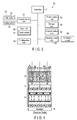
- FIG. 3 is a block diagram of the electronic watch 50.
- the electronic watch 50 comprises a controller 51, a power supply unit 52, a storage unit 53, a communication unit 54, a clocking circuit unit 55, an oscillation circuit 56, a display driving unit 57, a liquid crystal display unit 10, an input unit 58, and a tilt detecting unit 59.
- the power supply unit 52 provides various power supplies to modules in the electronic watch 50 via power supply lines.
- the power supply unit 52 comprises, for example, a button battery (primary battery).
- the storage unit 53 comprises, for example, a ROM (Read Only Memory) for data read, and a data readable and writable RAM (Random Access Memory).
- the storage unit 53 includes a system program for allowing various functions of the electronic watch 50 to be implemented, a program area in which application programs and the like are stored, and a data area in which various data such as image data are stored.
- the communication unit 54 controls communication (wireless communication) with other apparatuses via a network including the Internet. Furthermore, the communication unit 54 may have a function to control short-range wireless communication such as Bluetooth (registered trade mark) which is made with other apparatuses.
- short-range wireless communication such as Bluetooth (registered trade mark) which is made with other apparatuses.
- the oscillation circuit 56 constantly outputs a clock signal with a constant frequency.
- the clocking circuit unit 55 counts signals received from the oscillation circuit 56 to acquire the current time data and the like.
- the clocking circuit unit 55 outputs the acquired current time data and date data to the controller 51.
- the display driving unit 57 drives the liquid crystal display unit 10 based on control signals, data, and the like from the controller 51 to allow the liquid crystal display unit 10 to display various characters and various types of information. Furthermore, the display driving unit 57 individually drives the first liquid crystal panel (PD-LCD or PN-LCD) 12 and second liquid crystal panel (color LCD) 14, which are included in the liquid crystal display unit 10.
- PD-LCD or PN-LCD first liquid crystal panel
- PN-LCD second liquid crystal panel
- the input unit 58 includes a plurality of pushbuttons used to give instructions to execute various functions of the electronic watch 50, and the touch sensor 17 depicted in FIG. 1 .
- time setting, mode selection, or the like is executed based on the operation.
- the tilt detecting unit 59 detects a tilt of the display surface of the electronic watch 50. Specifically, the tilt detecting unit 59 detects the angle between the display surface of the electronic watch 50 and a vertical line (direction of gravity).
- the tilt detecting unit 59 comprises, for example, a three-axis acceleration sensor.
- the controller 51 controls the general operation of the electronic watch 50.
- the controller 51 comprises a CPU (Central Processing Unit).
- the controller 51 reads any of various programs stored in a ROM at a predetermined timing or in accordance with an operation signal or the like input via the input unit 58 and loads the program into a work area of a RAM.
- the controller 51 then instructs (controls) modules of the electronic watch 50, transfers data, or performs any other operation in accordance with the program.
- the electronic watch 50 comprises a camera function (imaging unit).
- FIG. 4 is a diagram illustrating an operation of the liquid crystal display unit 10 in the character display.
- the first liquid crystal panel 12 performs a display operation, while the second liquid crystal panel 14 is in an off state (the backlight 15 is also off).
- the second liquid crystal panel 14 is based on a normally black mode and provides black display in the off state.
- the liquid crystals are dispersed in the polymer network, and the liquid crystal molecules are randomly arranged at the time of voltage off (no electric field).
- n e refractive index of extraordinary light from liquid crystal molecules
- n o refractive index of ordinary light from liquid crystal molecules
- n o refractive index of the polymer network
- the air layer 13a which has a refractive index different from the refractive index of the lower substrate 20, is present under the lower substrate 20, light having reached the lower substrate 20 is reflected by the interface between the lower substrate 20 and the air layer 13a. As a result, the first liquid crystal panel 12 allows bright display to be achieved.
- individual control of the voltages of the plurality of display electrodes 24 allows control of areas in the off state and areas in the on state.
- An area in which the display electrode 24 is in the off state provides white display.
- An area in which the display electrode 24 is in the on state provides black display.
- any character display in the present embodiment, time display and standby display
- FIG. 5 is a diagram illustrating an operation of the liquid crystal display unit 10 in the information display.
- the backlight 15 is turned on, light from the backlight 15 enters the second liquid crystal panel 14. Moreover, the second liquid crystal panel 14 is driven, and the entire display surface of the first liquid crystal panel 12 is set to a transmissive state (transparent state). That is, the liquid crystal layer 22 in the first liquid crystal panel 12 is entirely set to the on state.
- the phase difference in the liquid crystal layer 32 is approximately zero.
- backlight light having transmitted through the polarizing plate 42 is transmitted through the liquid crystal layer 32 with approximately zero phase difference and absorbed by the polarizing plate 44 disposed in a crossed Nichol state with respect to the polarizing plate 42 to provide black display.
- the black display on the second liquid crystal panel 14 is viewed by the user via the first liquid crystal panel 12 in the transmissive state.
- the long axes of the liquid crystal molecules are tilted from the vertical direction.
- the phase difference in the liquid crystal layer 32 in this case is set approximately to ⁇ /2.
- backlight light having transmitted through the polarizing plate 42 is transmitted through the liquid crystal layer 32 and provided with a phase difference.
- the backlight light then transmits through the polarizing plate 44 to provide white display (color display).
- the color display on the second liquid crystal panel 14 is viewed by the user via the first liquid crystal panel 12 in the transmissive state.
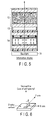
- FIG. 6 illustrates a detecting operation of the tilt detecting unit 59.
- a direction in which character strings are arranged in the display surface of the electronic watch 50 is defined as an X axis.
- a direction orthogonal to the X axis is defined as a Y axis.
- the angle between the X axis and the vertical line (the axis of anti-gravity) is defined as ⁇ .
- the angle between the Y axis and the vertical line is defined as ⁇ .
- the tilt detecting unit 59 determines how the X axis is inclined to the vertical line (what degree the angle ⁇ is) and how the Y axis is inclined to the vertical line (what degree the angle ⁇ is). It is assumed that "0° ⁇ ⁇ ⁇ 90° " and "0° ⁇ ⁇ ⁇ 90° ". That is, the angles ⁇ and ⁇ are each a smaller angle to the vertical line.
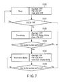
- FIG. 7 is a flowchart illustrating operations of the electronic watch 50. It is assumed that the electronic watch 50 is worn around the user's wrist.
- the controller 51 monitors detection results from the tilt detecting unit 59 (step S101). When the angle ⁇ is "0° ⁇ ⁇ ⁇ 30° ", the controller 51 sets the electronic watch 50 to a sleep mode (power saving mode) (step S100). The condition "0° ⁇ ⁇ ⁇ 30° " is intended to detect that the user is not viewing the display on the electronic watch 50.
- FIG. 8A is a diagram illustrating that the user is not viewing the display on the electronic watch 50. The user holds the user's arm wearing the electronic watch 50, substantially along the vertical line.
- the controller 51 turns all of the following off: the backlight 15, the first liquid crystal panel 12 (PD-LCD or PN-LCD), and the second liquid crystal panel (color LCD) 14.
- the power consumption f the electronic watch 50 can be reduced.
- step S101 upon determining that the angle ⁇ is at least 30°, the controller 51 sets the electronic watch 50 to a time display mode (step S102).
- the condition " ⁇ ⁇ 30° " is intended to detect that the user is viewing the display on the electronic watch 50.
- FIG. 8B is a diagram illustrating that the user is viewing the display on the electronic watch 50. The user holds the user's arm wearing the electronic watch 50, substantially in the horizontal direction. In this case, for example, " ⁇ ⁇ 80° and ⁇ ⁇ 90° ".
- the controller 51 turns the backlight 15 off, performs display driving on the first liquid crystal panel (PD-LCD or PN-LCD) 12, and turns the second liquid crystal panel (color LCD) 14 off.
- the user can view the time display as an example of the character display.
- the backlight 15 and the second liquid crystal panel (color LCD) 14 are off, allowing the power consumption of the electronic watch to be suppressed.
- the controller 51 monitors a detection result from the touch panel 11 (step S103).
- the controller 51 sets the electronic watch 50 to an information display mode (step S104).
- the controller 51 turns the backlight 15 on, turns the entire display surface of the first liquid crystal panel (PD-LCD or PN-LCD) 12 on (transmissive state), and performs display driving on the second liquid crystal panel (color LCD) 14.
- the electronic watch 50 displays information the amount of which is larger than in the character display and can perform color display.
- the controller 51 monitors a detection result from the touch panel 11 (step S105).
- the controller 51 returns to step S101 to monitor a detection result from the tilt detecting unit 59.
- FIG. 9 is a flowchart depicting operations of the electronic watch 50 according to a modification.
- the controller 51 determines, for a predetermined time, whether or not the user has performed an input operation via the input unit 58 (step S106).
- the controller 51 Upon determining in step S106 that the user has performed no input operation for the predetermined time, the controller 51 returns to step S101 to monitor a detection result from the tilt detecting unit 59.
- step S106 allows the user to shift the electronic watch 50 to the sleep mode even when forgetting to turn the information display mode off after the use of the information display mode. This enables prevention of a wasteful increase in the power consumption of the electronic watch 50.
- FIG. 10 is a block diagram of the electronic watch 50 according to a modification.
- the electronic watch 50 comprises a sensor 60 that determines whether or not the electronic watch 50 is worn around the user's wrist.
- the controller 51 sets the electronic watch 50 to the sleep mode. This enables a reduction in the power consumption of the electronic watch 50.
- the electronic watch (liquid crystal display) 50 comprises the liquid crystal display unit 10 with the first liquid crystal panel 12 and the second liquid crystal panel 14 laminated therein.
- the first liquid crystal panel 12 performs the character display including the time display.
- the second liquid crystal panel 14 performs the information display using a larger amount of information than the character display. Moreover, during the character display, the second liquid crystal panel 14 and backlight 15, which consume a large amount of power, are off.
- both the character display and the information display can be performed, and the power consumption during the character display can be reduced.
- display time can be drastically increased.
- the air layer 13a is provided in contact with the lower substrate 20 of the first liquid crystal panel 12.
- reflected light reflected by the interface between the lower substrate 20 and the air layer 13a can be utilized for display, allowing brighter display to be achieved.
- the electronic watch 50 is set to the sleep mode.
- the backlight 15, the first liquid crystal panel (PD-LCD or PN-LCD) 12, and the second liquid crystal panel (color LCD) 14 are all off. This enables a reduction in the power consumption of the electronic watch 50.
- the electronic watch 50 comprises the touch panel 11 that can be easily operated by the user.
- the display mode is switched depending on a touch operation detected by the touch panel 11.
- the display modes can be easily switched.
- a second embodiment is a configuration example in which a semi-transmissive liquid crystal panel is used as a second liquid crystal panel 14.
- FIG. 11 is a cross-sectional view of a liquid crystal display unit 10 according to the second embodiment.
- Pixels 34 in the second liquid crystal panel 14 each comprise a reflective area 34R and a transmissive area 34T.
- the reflective area 34R corresponds to an area of the pixel 34 in which a reflective film 45 is provided.
- the transmissive area 34T corresponds to an area of the pixel in which the reflective film 45 is not provided.
- the reflective film 45 is formed on a TFT substrate 30 and has a function to reflect outside light incident through a display surface of the liquid crystal display unit 10.
- Aluminum (Al) is used as the reflective film 45.
- the second embodiment is the same as the first embodiment.
- liquid crystal display unit 10 configured as described above, when the display on the liquid crystal display unit 10 is viewed in a bright outdoor environment, reflected light from the reflective area 34R of the second liquid crystal panel 14 can be utilized for display. This improves the outdoor visibility of the liquid crystal display unit 10 and allows the information display on the second liquid crystal panel 14 to be made brighter.
- the watch has been illustrated as the electronic equipment.
- the liquid crystal display unit 10 with the first liquid crystal panel 12 and the second liquid crystal panel 14 laminated therein may be applied to small, potable shapes such as cellular phones and portable information terminals and other types of electronic equipment such as displays, computers, and cameras which serve as wearable devices carried by the user.
- the present invention is not limited to the embodiments described above, and can be embodied by modifying constituent elements without departing from the gist of the invention.
- the above embodiments include inventions of various stages, and various inventions can be formed by proper combinations of a plurality of constituent elements disclosed in one embodiment or proper combinations of constituent elements disclosed in different embodiments.
- the problems to be solved by the present invention can be solved and the effects of the invention can be obtained even if several constituent elements are omitted from all the constituent elements disclosed in each embodiment, an embodiment from which these constituent elements are omitted can be extracted as an invention.
- liquid crystal display unit 11: touch panel, 12: first liquid crystal panel, 13: transparent member, 14: second liquid crystal panel, 15: backlight, 16: transparent substrate, 17: touch sensor, 18, 26, 33: seal member, 20: lower substrate, 21: upper substrate, 22: liquid crystal layer, 23: common electrode, 24: display electrode, 25: polymer network, 27: UV cut film, 30: TFT substrate, 31: CF substrate, 32: liquid crystal layer, 34: pixel, 35: TFT, 36: pixel electrode, 37, 40: orientation film, 38: color filter, 39: common electrode, 41, 43: phase plate, 42, 44: polarizing plate, 45: reflective film, 50: liquid crystal display, 51: controller, 52: power supply unit, 53: storage unit, 54: communication unit, 55: clocking circuit unit, 56: oscillation circuit, 57: display driving unit, 58: input unit, 59: tilt detecting unit, 60: sensor
Landscapes
- Physics & Mathematics (AREA)
- Nonlinear Science (AREA)
- Chemical & Material Sciences (AREA)
- General Physics & Mathematics (AREA)
- Crystallography & Structural Chemistry (AREA)
- Optics & Photonics (AREA)
- Mathematical Physics (AREA)
- Dispersion Chemistry (AREA)
- Engineering & Computer Science (AREA)
- Theoretical Computer Science (AREA)
- Computer Hardware Design (AREA)
- Inorganic Chemistry (AREA)
- Liquid Crystal (AREA)
- Control Of Indicators Other Than Cathode Ray Tubes (AREA)
- Electric Clocks (AREA)
- Liquid Crystal Display Device Control (AREA)
- Devices For Indicating Variable Information By Combining Individual Elements (AREA)
Applications Claiming Priority (2)
| Application Number | Priority Date | Filing Date | Title |
|---|---|---|---|
| JP2013019689 | 2013-02-04 | ||
| PCT/JP2014/050841 WO2014119395A1 (ja) | 2013-02-04 | 2014-01-17 | 液晶表示装置 |
Publications (3)
| Publication Number | Publication Date |
|---|---|
| EP2952955A1 true EP2952955A1 (de) | 2015-12-09 |
| EP2952955A4 EP2952955A4 (de) | 2016-07-20 |
| EP2952955B1 EP2952955B1 (de) | 2022-02-23 |
Family
ID=51262109
Family Applications (1)
| Application Number | Title | Priority Date | Filing Date |
|---|---|---|---|
| EP14745937.4A Active EP2952955B1 (de) | 2013-02-04 | 2014-01-17 | Flüssigkristallanzeige |
Country Status (6)
| Country | Link |
|---|---|
| US (1) | US10025150B2 (de) |
| EP (1) | EP2952955B1 (de) |
| JP (1) | JP5640178B1 (de) |
| KR (1) | KR101660657B1 (de) |
| CN (1) | CN104620170A (de) |
| WO (1) | WO2014119395A1 (de) |
Cited By (1)
| Publication number | Priority date | Publication date | Assignee | Title |
|---|---|---|---|---|
| CN112711152A (zh) * | 2020-12-31 | 2021-04-27 | 武汉华星光电技术有限公司 | 一种液晶显示面板和液晶显示装置 |
Families Citing this family (25)
| Publication number | Priority date | Publication date | Assignee | Title |
|---|---|---|---|---|
| KR20150083742A (ko) * | 2014-01-10 | 2015-07-20 | 삼성전자주식회사 | 디스플레이 장치 및 이의 제조방법 |
| HK1203120A2 (en) * | 2014-08-26 | 2015-10-16 | Well Being Digital Limited | A gait monitor and a method of monitoring the gait of a person |
| JP6176289B2 (ja) * | 2014-09-22 | 2017-08-09 | カシオ計算機株式会社 | 表示装置、制御方法及びプログラム |
| WO2016194232A1 (ja) | 2015-06-05 | 2016-12-08 | 日立マクセル株式会社 | 映像表示装置および制御方法 |
| MA42412A (fr) * | 2015-07-06 | 2018-05-16 | Enlighten Entpr Inc | Système d'éclairement |
| JP6146594B1 (ja) * | 2015-12-22 | 2017-06-14 | カシオ計算機株式会社 | 表示装置及びその制御方法、制御プログラム |
| JP6341192B2 (ja) * | 2015-12-22 | 2018-06-13 | カシオ計算機株式会社 | 情報処理装置、制御方法及びプログラム |
| JP6699166B2 (ja) * | 2015-12-24 | 2020-05-27 | カシオ計算機株式会社 | 表示制御装置、表示制御方法及びプログラム |
| JP2017161701A (ja) * | 2016-03-09 | 2017-09-14 | 株式会社 オルタステクノロジー | 表示装置 |
| JP2017167352A (ja) * | 2016-03-16 | 2017-09-21 | 株式会社 オルタステクノロジー | 表示装置 |
| JP6897002B2 (ja) * | 2016-04-11 | 2021-06-30 | 凸版印刷株式会社 | 表示装置 |
| US9791833B1 (en) * | 2016-04-13 | 2017-10-17 | Google Inc. | Physical watch hands for a computerized watch |
| JP2018004927A (ja) * | 2016-07-01 | 2018-01-11 | 株式会社半導体エネルギー研究所 | 表示装置、入出力装置、情報処理装置、表示方法 |
| CN106125387B (zh) * | 2016-08-23 | 2019-07-30 | 中节能万润股份有限公司 | 一种pdlc显示器和pdlc电子阅读器 |
| US10232282B2 (en) * | 2016-12-08 | 2019-03-19 | Disney Enterprises, Inc. | Display system for transforming sunlit surfaces |
| JP2018170605A (ja) * | 2017-03-29 | 2018-11-01 | 京セラ株式会社 | 携帯電子機器、制御方法、及び制御プログラム |
| JP2017146614A (ja) * | 2017-04-28 | 2017-08-24 | カシオ計算機株式会社 | 表示装置、電子機器及びその制御方法、制御プログラム |
| JP2019008200A (ja) * | 2017-06-27 | 2019-01-17 | 株式会社 オルタステクノロジー | 電子機器 |
| US9964827B1 (en) * | 2017-07-18 | 2018-05-08 | A.U. Vista, Inc. | Light control device and display device using the same |
| KR102380640B1 (ko) * | 2017-11-23 | 2022-03-29 | 엘지디스플레이 주식회사 | 액정캡슐을 포함하는 액정표시장치 |
| JP2019159226A (ja) * | 2018-03-16 | 2019-09-19 | カシオ計算機株式会社 | 電子機器、その表示制御方法及び表示制御プログラム |
| JP7109957B2 (ja) | 2018-03-27 | 2022-08-01 | 株式会社ジャパンディスプレイ | 表示装置 |
| JP6793779B2 (ja) * | 2019-05-20 | 2020-12-02 | シャープ株式会社 | 画像処理装置及び画像処理方法 |
| JP6743254B2 (ja) * | 2019-08-08 | 2020-08-19 | マクセル株式会社 | 映像表示装置および制御方法 |
| CN119148432A (zh) * | 2023-06-15 | 2024-12-17 | 群创光电股份有限公司 | 电子装置 |
Family Cites Families (20)
| Publication number | Priority date | Publication date | Assignee | Title |
|---|---|---|---|---|
| US5264952A (en) * | 1989-11-20 | 1993-11-23 | Sharp Kabushiki Kaisha | Two celled color liquid crystal display device |
| DE69228843T2 (de) | 1991-05-27 | 1999-08-26 | Dainippon Ink And Chemicals | Flüssigkristallvorrichtung |
| JPH05273576A (ja) * | 1991-07-09 | 1993-10-22 | Dainippon Ink & Chem Inc | 光散乱形液晶2層パネル |
| AU8461098A (en) * | 1997-07-30 | 1999-02-22 | Citizen Watch Co. Ltd. | Liquid crystal display |
| AU8462798A (en) * | 1997-08-01 | 1999-02-22 | Citizen Watch Co. Ltd. | Liquid crystal display panel for timepieces |
| US6128053A (en) * | 1997-10-22 | 2000-10-03 | Mannesmann Vdo Ag | Liquid crystal display with heater |
| JPH11160682A (ja) * | 1997-11-26 | 1999-06-18 | Casio Comput Co Ltd | 反射型液晶表示素子 |
| JP2000214277A (ja) | 1999-01-22 | 2000-08-04 | Citizen Watch Co Ltd | 情報端末機能付き腕時計 |
| JP2004117652A (ja) | 2002-09-25 | 2004-04-15 | Rohm Co Ltd | 複合表示装置 |
| US7593755B2 (en) | 2004-09-15 | 2009-09-22 | Microsoft Corporation | Display of wireless data |
| KR20060122698A (ko) * | 2005-05-26 | 2006-11-30 | 삼성전자주식회사 | 표시 장치 및 이를 포함하는 휴대용 표시 장치 |
| JP2007232882A (ja) | 2006-02-28 | 2007-09-13 | Casio Comput Co Ltd | 表示装置及び電子機器 |
| JP4669811B2 (ja) * | 2006-05-01 | 2011-04-13 | Nec液晶テクノロジー株式会社 | 光線制御用フィルム装置,光線制御装置,照明角度可変光源及びこれを備えた表示装置並びに端末装置 |
| JP5135715B2 (ja) | 2006-05-31 | 2013-02-06 | トヨタ自動車株式会社 | 密閉型電池及びその製造方法 |
| KR100758986B1 (ko) * | 2006-07-14 | 2007-09-17 | 삼성전자주식회사 | 듀얼 액정 디스플레이 장치 |
| EP2249330A1 (de) * | 2008-02-22 | 2010-11-10 | Sharp Kabushiki Kaisha | Anzeigeeinrichtung |
| WO2010011779A2 (en) * | 2008-07-23 | 2010-01-28 | Flextronics Ap, Llc | Integration design for capacitive touch panels and liquid crystal displays |
| JP2010211084A (ja) * | 2009-03-12 | 2010-09-24 | Casio Computer Co Ltd | 表示装置 |
| JP5299776B2 (ja) * | 2009-06-30 | 2013-09-25 | Nltテクノロジー株式会社 | 液晶表示素子、表示装置及びその駆動方法 |
| JP2011059589A (ja) * | 2009-09-14 | 2011-03-24 | Sony Ericsson Mobilecommunications Japan Inc | 表示装置、携帯情報端末、携帯情報端末の表示制御方法及び表示制御プログラム、 |
-
2014
- 2014-01-17 KR KR1020157006380A patent/KR101660657B1/ko active Active
- 2014-01-17 WO PCT/JP2014/050841 patent/WO2014119395A1/ja not_active Ceased
- 2014-01-17 JP JP2014531037A patent/JP5640178B1/ja not_active Expired - Fee Related
- 2014-01-17 EP EP14745937.4A patent/EP2952955B1/de active Active
- 2014-01-17 CN CN201480002343.XA patent/CN104620170A/zh active Pending
-
2015
- 2015-03-11 US US14/644,780 patent/US10025150B2/en active Active
Cited By (1)
| Publication number | Priority date | Publication date | Assignee | Title |
|---|---|---|---|---|
| CN112711152A (zh) * | 2020-12-31 | 2021-04-27 | 武汉华星光电技术有限公司 | 一种液晶显示面板和液晶显示装置 |
Also Published As
| Publication number | Publication date |
|---|---|
| KR101660657B1 (ko) | 2016-09-27 |
| EP2952955B1 (de) | 2022-02-23 |
| KR20150043432A (ko) | 2015-04-22 |
| US10025150B2 (en) | 2018-07-17 |
| EP2952955A4 (de) | 2016-07-20 |
| JP5640178B1 (ja) | 2014-12-10 |
| JPWO2014119395A1 (ja) | 2017-01-26 |
| WO2014119395A1 (ja) | 2014-08-07 |
| US20150185518A1 (en) | 2015-07-02 |
| CN104620170A (zh) | 2015-05-13 |
Similar Documents
| Publication | Publication Date | Title |
|---|---|---|
| EP2952955B1 (de) | Flüssigkristallanzeige | |
| JP4572888B2 (ja) | 液晶装置及び電子機器 | |
| KR101721889B1 (ko) | 능동형유기발광다이오드 표시장치 및 그의 표시제어방법 | |
| CN110501823A (zh) | 可切换视角控制装置和显示系统 | |
| KR20150123915A (ko) | 로컬 디밍 요소들을 갖는 디스플레이들 | |
| KR20110081069A (ko) | 액정 표시 장치 | |
| US20200124917A1 (en) | Electronic device | |
| CN104460138A (zh) | 一种可切换视角的液晶显示面板及其驱动方法 | |
| US20190384112A1 (en) | Double-sided display device and display module thereof | |
| US8310435B2 (en) | Liquid crystal display device capable of automatically switching to a mode and method for driving the same | |
| JP2001305525A (ja) | 液晶表示素子 | |
| CN209821552U (zh) | 液晶显示面板及显示装置 | |
| US9759957B2 (en) | Transflective liquid crystal display panel and a liquid crystal display device | |
| KR100671160B1 (ko) | 반투과형 액정 표시 장치 및 그 제조 방법 | |
| KR101251405B1 (ko) | 액정 표시장치 | |
| US8400386B2 (en) | Transflective liquid crystal display device | |
| US11428997B2 (en) | Liquid crystal panel | |
| KR100843477B1 (ko) | 듀얼 프론트 라이트를 이용한 듀얼 액정표시장치 | |
| JP2009271211A (ja) | 液晶表示装置及びそれを用いた電子機器並びに液晶表示装置の表示方法 | |
| KR20130033618A (ko) | 투명 액정표시장치 | |
| KR20080060822A (ko) | 액정 표시장치 | |
| JP2009157297A (ja) | 液晶表示装置 | |
| KR100765434B1 (ko) | 반투과형 디스플레이 장치 | |
| JP2009086117A (ja) | 透過型液晶表示装置及び電子機器 | |
| JP2008139583A (ja) | ディスプレイおよびそれに用いられる視野角制御装置 |
Legal Events
| Date | Code | Title | Description |
|---|---|---|---|
| PUAI | Public reference made under article 153(3) epc to a published international application that has entered the european phase |
Free format text: ORIGINAL CODE: 0009012 |
|
| 17P | Request for examination filed |
Effective date: 20150313 |
|
| AK | Designated contracting states |
Kind code of ref document: A1 Designated state(s): AL AT BE BG CH CY CZ DE DK EE ES FI FR GB GR HR HU IE IS IT LI LT LU LV MC MK MT NL NO PL PT RO RS SE SI SK SM TR |
|
| AX | Request for extension of the european patent |
Extension state: BA ME |
|
| DAX | Request for extension of the european patent (deleted) | ||
| RIC1 | Information provided on ipc code assigned before grant |
Ipc: G02F 1/1334 20060101AFI20160609BHEP Ipc: G02F 1/1347 20060101ALN20160609BHEP |
|
| A4 | Supplementary search report drawn up and despatched |
Effective date: 20160617 |
|
| STAA | Information on the status of an ep patent application or granted ep patent |
Free format text: STATUS: EXAMINATION IS IN PROGRESS |
|
| RIC1 | Information provided on ipc code assigned before grant |
Ipc: G02F 1/1347 20060101ALN20170502BHEP Ipc: G02F 1/1334 20060101AFI20170502BHEP |
|
| 17Q | First examination report despatched |
Effective date: 20170522 |
|
| RIC1 | Information provided on ipc code assigned before grant |
Ipc: G02F 1/1347 20060101ALN20190430BHEP Ipc: G02F 1/1334 20060101AFI20190430BHEP Ipc: G02F 1/1335 20060101ALN20190430BHEP |
|
| RAP1 | Party data changed (applicant data changed or rights of an application transferred) |
Owner name: TOPPAN PRINTING CO., LTD. |
|
| GRAP | Despatch of communication of intention to grant a patent |
Free format text: ORIGINAL CODE: EPIDOSNIGR1 |
|
| STAA | Information on the status of an ep patent application or granted ep patent |
Free format text: STATUS: GRANT OF PATENT IS INTENDED |
|
| RIC1 | Information provided on ipc code assigned before grant |
Ipc: G02F 1/1335 20060101ALN20210914BHEP Ipc: G02F 1/1347 20060101ALN20210914BHEP Ipc: G02F 1/1334 20060101AFI20210914BHEP |
|
| INTG | Intention to grant announced |
Effective date: 20210928 |
|
| GRAS | Grant fee paid |
Free format text: ORIGINAL CODE: EPIDOSNIGR3 |
|
| GRAA | (expected) grant |
Free format text: ORIGINAL CODE: 0009210 |
|
| STAA | Information on the status of an ep patent application or granted ep patent |
Free format text: STATUS: THE PATENT HAS BEEN GRANTED |
|
| AK | Designated contracting states |
Kind code of ref document: B1 Designated state(s): AL AT BE BG CH CY CZ DE DK EE ES FI FR GB GR HR HU IE IS IT LI LT LU LV MC MK MT NL NO PL PT RO RS SE SI SK SM TR |
|
| REG | Reference to a national code |
Ref country code: GB Ref legal event code: FG4D |
|
| REG | Reference to a national code |
Ref country code: CH Ref legal event code: EP |
|
| REG | Reference to a national code |
Ref country code: AT Ref legal event code: REF Ref document number: 1470910 Country of ref document: AT Kind code of ref document: T Effective date: 20220315 |
|
| REG | Reference to a national code |
Ref country code: IE Ref legal event code: FG4D |
|
| REG | Reference to a national code |
Ref country code: DE Ref legal event code: R096 Ref document number: 602014082573 Country of ref document: DE |
|
| REG | Reference to a national code |
Ref country code: FI Ref legal event code: FGE |
|
| REG | Reference to a national code |
Ref country code: SE Ref legal event code: TRGR |
|
| REG | Reference to a national code |
Ref country code: LT Ref legal event code: MG9D |
|
| REG | Reference to a national code |
Ref country code: NL Ref legal event code: MP Effective date: 20220223 |
|
| REG | Reference to a national code |
Ref country code: AT Ref legal event code: MK05 Ref document number: 1470910 Country of ref document: AT Kind code of ref document: T Effective date: 20220223 |
|
| PG25 | Lapsed in a contracting state [announced via postgrant information from national office to epo] |
Ref country code: RS Free format text: LAPSE BECAUSE OF FAILURE TO SUBMIT A TRANSLATION OF THE DESCRIPTION OR TO PAY THE FEE WITHIN THE PRESCRIBED TIME-LIMIT Effective date: 20220223 Ref country code: PT Free format text: LAPSE BECAUSE OF FAILURE TO SUBMIT A TRANSLATION OF THE DESCRIPTION OR TO PAY THE FEE WITHIN THE PRESCRIBED TIME-LIMIT Effective date: 20220623 Ref country code: NO Free format text: LAPSE BECAUSE OF FAILURE TO SUBMIT A TRANSLATION OF THE DESCRIPTION OR TO PAY THE FEE WITHIN THE PRESCRIBED TIME-LIMIT Effective date: 20220523 Ref country code: NL Free format text: LAPSE BECAUSE OF FAILURE TO SUBMIT A TRANSLATION OF THE DESCRIPTION OR TO PAY THE FEE WITHIN THE PRESCRIBED TIME-LIMIT Effective date: 20220223 Ref country code: LT Free format text: LAPSE BECAUSE OF FAILURE TO SUBMIT A TRANSLATION OF THE DESCRIPTION OR TO PAY THE FEE WITHIN THE PRESCRIBED TIME-LIMIT Effective date: 20220223 Ref country code: HR Free format text: LAPSE BECAUSE OF FAILURE TO SUBMIT A TRANSLATION OF THE DESCRIPTION OR TO PAY THE FEE WITHIN THE PRESCRIBED TIME-LIMIT Effective date: 20220223 Ref country code: ES Free format text: LAPSE BECAUSE OF FAILURE TO SUBMIT A TRANSLATION OF THE DESCRIPTION OR TO PAY THE FEE WITHIN THE PRESCRIBED TIME-LIMIT Effective date: 20220223 Ref country code: BG Free format text: LAPSE BECAUSE OF FAILURE TO SUBMIT A TRANSLATION OF THE DESCRIPTION OR TO PAY THE FEE WITHIN THE PRESCRIBED TIME-LIMIT Effective date: 20220523 |
|
| PG25 | Lapsed in a contracting state [announced via postgrant information from national office to epo] |
Ref country code: PL Free format text: LAPSE BECAUSE OF FAILURE TO SUBMIT A TRANSLATION OF THE DESCRIPTION OR TO PAY THE FEE WITHIN THE PRESCRIBED TIME-LIMIT Effective date: 20220223 Ref country code: LV Free format text: LAPSE BECAUSE OF FAILURE TO SUBMIT A TRANSLATION OF THE DESCRIPTION OR TO PAY THE FEE WITHIN THE PRESCRIBED TIME-LIMIT Effective date: 20220223 Ref country code: GR Free format text: LAPSE BECAUSE OF FAILURE TO SUBMIT A TRANSLATION OF THE DESCRIPTION OR TO PAY THE FEE WITHIN THE PRESCRIBED TIME-LIMIT Effective date: 20220524 Ref country code: AT Free format text: LAPSE BECAUSE OF FAILURE TO SUBMIT A TRANSLATION OF THE DESCRIPTION OR TO PAY THE FEE WITHIN THE PRESCRIBED TIME-LIMIT Effective date: 20220223 |
|
| PG25 | Lapsed in a contracting state [announced via postgrant information from national office to epo] |
Ref country code: IS Free format text: LAPSE BECAUSE OF FAILURE TO SUBMIT A TRANSLATION OF THE DESCRIPTION OR TO PAY THE FEE WITHIN THE PRESCRIBED TIME-LIMIT Effective date: 20220623 |
|
| PG25 | Lapsed in a contracting state [announced via postgrant information from national office to epo] |
Ref country code: SM Free format text: LAPSE BECAUSE OF FAILURE TO SUBMIT A TRANSLATION OF THE DESCRIPTION OR TO PAY THE FEE WITHIN THE PRESCRIBED TIME-LIMIT Effective date: 20220223 Ref country code: SK Free format text: LAPSE BECAUSE OF FAILURE TO SUBMIT A TRANSLATION OF THE DESCRIPTION OR TO PAY THE FEE WITHIN THE PRESCRIBED TIME-LIMIT Effective date: 20220223 Ref country code: RO Free format text: LAPSE BECAUSE OF FAILURE TO SUBMIT A TRANSLATION OF THE DESCRIPTION OR TO PAY THE FEE WITHIN THE PRESCRIBED TIME-LIMIT Effective date: 20220223 Ref country code: EE Free format text: LAPSE BECAUSE OF FAILURE TO SUBMIT A TRANSLATION OF THE DESCRIPTION OR TO PAY THE FEE WITHIN THE PRESCRIBED TIME-LIMIT Effective date: 20220223 Ref country code: DK Free format text: LAPSE BECAUSE OF FAILURE TO SUBMIT A TRANSLATION OF THE DESCRIPTION OR TO PAY THE FEE WITHIN THE PRESCRIBED TIME-LIMIT Effective date: 20220223 Ref country code: CZ Free format text: LAPSE BECAUSE OF FAILURE TO SUBMIT A TRANSLATION OF THE DESCRIPTION OR TO PAY THE FEE WITHIN THE PRESCRIBED TIME-LIMIT Effective date: 20220223 |
|
| REG | Reference to a national code |
Ref country code: DE Ref legal event code: R097 Ref document number: 602014082573 Country of ref document: DE |
|
| PG25 | Lapsed in a contracting state [announced via postgrant information from national office to epo] |
Ref country code: AL Free format text: LAPSE BECAUSE OF FAILURE TO SUBMIT A TRANSLATION OF THE DESCRIPTION OR TO PAY THE FEE WITHIN THE PRESCRIBED TIME-LIMIT Effective date: 20220223 |
|
| PLBE | No opposition filed within time limit |
Free format text: ORIGINAL CODE: 0009261 |
|
| STAA | Information on the status of an ep patent application or granted ep patent |
Free format text: STATUS: NO OPPOSITION FILED WITHIN TIME LIMIT |
|
| 26N | No opposition filed |
Effective date: 20221124 |
|
| PG25 | Lapsed in a contracting state [announced via postgrant information from national office to epo] |
Ref country code: SI Free format text: LAPSE BECAUSE OF FAILURE TO SUBMIT A TRANSLATION OF THE DESCRIPTION OR TO PAY THE FEE WITHIN THE PRESCRIBED TIME-LIMIT Effective date: 20220223 |
|
| P01 | Opt-out of the competence of the unified patent court (upc) registered |
Effective date: 20230530 |
|
| PG25 | Lapsed in a contracting state [announced via postgrant information from national office to epo] |
Ref country code: IT Free format text: LAPSE BECAUSE OF FAILURE TO SUBMIT A TRANSLATION OF THE DESCRIPTION OR TO PAY THE FEE WITHIN THE PRESCRIBED TIME-LIMIT Effective date: 20220223 |
|
| REG | Reference to a national code |
Ref country code: CH Ref legal event code: PL |
|
| PG25 | Lapsed in a contracting state [announced via postgrant information from national office to epo] |
Ref country code: LU Free format text: LAPSE BECAUSE OF NON-PAYMENT OF DUE FEES Effective date: 20230117 |
|
| REG | Reference to a national code |
Ref country code: BE Ref legal event code: MM Effective date: 20230131 |
|
| PG25 | Lapsed in a contracting state [announced via postgrant information from national office to epo] |
Ref country code: LI Free format text: LAPSE BECAUSE OF NON-PAYMENT OF DUE FEES Effective date: 20230131 Ref country code: CH Free format text: LAPSE BECAUSE OF NON-PAYMENT OF DUE FEES Effective date: 20230131 |
|
| PG25 | Lapsed in a contracting state [announced via postgrant information from national office to epo] |
Ref country code: BE Free format text: LAPSE BECAUSE OF NON-PAYMENT OF DUE FEES Effective date: 20230131 |
|
| PG25 | Lapsed in a contracting state [announced via postgrant information from national office to epo] |
Ref country code: IE Free format text: LAPSE BECAUSE OF NON-PAYMENT OF DUE FEES Effective date: 20230117 |
|
| PG25 | Lapsed in a contracting state [announced via postgrant information from national office to epo] |
Ref country code: MC Free format text: LAPSE BECAUSE OF FAILURE TO SUBMIT A TRANSLATION OF THE DESCRIPTION OR TO PAY THE FEE WITHIN THE PRESCRIBED TIME-LIMIT Effective date: 20220223 |
|
| PG25 | Lapsed in a contracting state [announced via postgrant information from national office to epo] |
Ref country code: MC Free format text: LAPSE BECAUSE OF FAILURE TO SUBMIT A TRANSLATION OF THE DESCRIPTION OR TO PAY THE FEE WITHIN THE PRESCRIBED TIME-LIMIT Effective date: 20220223 |
|
| PGFP | Annual fee paid to national office [announced via postgrant information from national office to epo] |
Ref country code: GB Payment date: 20241128 Year of fee payment: 12 |
|
| PGFP | Annual fee paid to national office [announced via postgrant information from national office to epo] |
Ref country code: FR Payment date: 20241209 Year of fee payment: 12 |
|
| PGFP | Annual fee paid to national office [announced via postgrant information from national office to epo] |
Ref country code: SE Payment date: 20241212 Year of fee payment: 12 |
|
| PGFP | Annual fee paid to national office [announced via postgrant information from national office to epo] |
Ref country code: DE Payment date: 20241203 Year of fee payment: 12 |
|
| PGFP | Annual fee paid to national office [announced via postgrant information from national office to epo] |
Ref country code: FI Payment date: 20250114 Year of fee payment: 12 |
|
| PG25 | Lapsed in a contracting state [announced via postgrant information from national office to epo] |
Ref country code: CY Free format text: LAPSE BECAUSE OF FAILURE TO SUBMIT A TRANSLATION OF THE DESCRIPTION OR TO PAY THE FEE WITHIN THE PRESCRIBED TIME-LIMIT; INVALID AB INITIO Effective date: 20140117 |
|
| PG25 | Lapsed in a contracting state [announced via postgrant information from national office to epo] |
Ref country code: HU Free format text: LAPSE BECAUSE OF FAILURE TO SUBMIT A TRANSLATION OF THE DESCRIPTION OR TO PAY THE FEE WITHIN THE PRESCRIBED TIME-LIMIT; INVALID AB INITIO Effective date: 20140117 |
|
| PG25 | Lapsed in a contracting state [announced via postgrant information from national office to epo] |
Ref country code: TR Free format text: LAPSE BECAUSE OF FAILURE TO SUBMIT A TRANSLATION OF THE DESCRIPTION OR TO PAY THE FEE WITHIN THE PRESCRIBED TIME-LIMIT Effective date: 20220223 |