EP2952996A1 - Étage de collecteur de courant pour LDO - Google Patents
Étage de collecteur de courant pour LDO Download PDFInfo
- Publication number
- EP2952996A1 EP2952996A1 EP15150230.9A EP15150230A EP2952996A1 EP 2952996 A1 EP2952996 A1 EP 2952996A1 EP 15150230 A EP15150230 A EP 15150230A EP 2952996 A1 EP2952996 A1 EP 2952996A1
- Authority
- EP
- European Patent Office
- Prior art keywords
- current
- ldo
- transistor
- voltage
- output voltage
- Prior art date
- Legal status (The legal status is an assumption and is not a legal conclusion. Google has not performed a legal analysis and makes no representation as to the accuracy of the status listed.)
- Granted
Links
Images



Classifications
-
- G—PHYSICS
- G05—CONTROLLING; REGULATING
- G05F—SYSTEMS FOR REGULATING ELECTRIC OR MAGNETIC VARIABLES
- G05F1/00—Automatic systems in which deviations of an electric quantity from one or more predetermined values are detected at the output of the system and fed back to a device within the system to restore the detected quantity to its predetermined value or values, i.e. retroactive systems
- G05F1/10—Regulating voltage or current
- G05F1/46—Regulating voltage or current wherein the variable actually regulated by the final control device is DC
- G05F1/56—Regulating voltage or current wherein the variable actually regulated by the final control device is DC using semiconductor devices in series with the load as final control devices
- G05F1/575—Regulating voltage or current wherein the variable actually regulated by the final control device is DC using semiconductor devices in series with the load as final control devices characterised by the feedback circuit
-
- G—PHYSICS
- G05—CONTROLLING; REGULATING
- G05F—SYSTEMS FOR REGULATING ELECTRIC OR MAGNETIC VARIABLES
- G05F1/00—Automatic systems in which deviations of an electric quantity from one or more predetermined values are detected at the output of the system and fed back to a device within the system to restore the detected quantity to its predetermined value or values, i.e. retroactive systems
- G05F1/10—Regulating voltage or current
- G05F1/46—Regulating voltage or current wherein the variable actually regulated by the final control device is DC
- G05F1/56—Regulating voltage or current wherein the variable actually regulated by the final control device is DC using semiconductor devices in series with the load as final control devices
-
- G—PHYSICS
- G05—CONTROLLING; REGULATING
- G05F—SYSTEMS FOR REGULATING ELECTRIC OR MAGNETIC VARIABLES
- G05F3/00—Non-retroactive systems for regulating electric variables by using an uncontrolled element, or an uncontrolled combination of elements, such element or such combination having self-regulating properties
- G05F3/02—Regulating voltage or current
- G05F3/08—Regulating voltage or current wherein the variable is DC
- G05F3/10—Regulating voltage or current wherein the variable is DC using uncontrolled devices with non-linear characteristics
- G05F3/16—Regulating voltage or current wherein the variable is DC using uncontrolled devices with non-linear characteristics being semiconductor devices
- G05F3/20—Regulating voltage or current wherein the variable is DC using uncontrolled devices with non-linear characteristics being semiconductor devices using diode- transistor combinations
- G05F3/26—Current mirrors
- G05F3/267—Current mirrors using both bipolar and field-effect technology
Definitions
- the present document relates to DC-to-DC converters.
- the present document relates to a current sink stage for low drop-out (LDO) regulators.
- LDO low drop-out
- LDOs are traditionally unidirectional power supplies i.e. they can either sink or source current.
- a common way to reduce the dip in the output voltage is to increase the output decoupling capacitor which means a larger footprint on the very expensive PCB real estate especially in the case of handheld devices.
- bi-directional push-pull LDOs may be a solution but they are very complex to compensate and require additional quiescent current.
- the additional current eats into a very tight power budget for a PMIC in low power mode.
- a current sink is implemented using either a comparator or an amplifier. Both have advantages and disadvantages.
- An amplifier would regulate the voltage at the output by regulating the current it sinks depending on the current sourced into the output of LDO, but are difficult to compensate.
- Comparators on the other hand don't require any compensation but may suffer from chattering and they don't regulate the output voltage if current pushed into the LDO output is less than the current sink capability of the comparator.
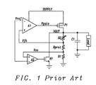
- Fig. 1 prior art shows a simplified schematic of an implementation of an LDO with a current sink or over-voltage sink.
- P1 is the pass device and A1 is an amplifier controlling the gate of P1 .
- R2, R1 & Rprot form a feedback resistor divider network for regulating the output voltage.
- C1 is an external decoupling capacitor.
- the load is an external IC powered by the LDO
- A2 and transistor N1 form an over-voltage sink.
- A2 can be configured as a comparator or as an amplifier. Under normal operation Vov is lower than the reference voltage Vref and the gate of N1 is pulled to ground, so no current is sunk from the output. In an overvoltage condition, if the voltage at Vov is higher than or equal to Vref, the current sink is activated. The gate of N1 is driven by A2 to sink the current from output voltage VOUT .
- A2 is configured as a comparator, the gate of N1 is driven either to supply or ground. If A2 along with N1 and capacitor C1 is configured as an amplifier, the gate of N1 is regulated depending on the difference between Vov and Vref
- Fig. 2 prior art shows a plot of a response of the LDO of Fig. 1 , wherein A2 is configured as a comparator and a current of 1 mA is sourced into the output of the LDO.
- A2 is configured as a comparator and a current of 1 mA is sourced into the output of the LDO.
- As the current sourced is lower than the sink capability of comparator we observe a 20mV of saw tooth at the output of LDO.
- the gate of N1 swings between ground and supply voltage. If such an LDO has to power a sensitive analog chip, such a saw tooth response at the output is undesirable.
- the output voltage when the sourced current is removed, raises nearly 35mV above the regulated target voltage and all the internal nodes of LDO are completely skewed at this point.
- Fig. 3 prior art shows a plot of a response of the LDO of Fig. 1 , wherein A2 is configured as an amplifier and a current of 1 mA is sourced into the output of the LDO.
- A2 is configured as an amplifier and a current of 1 mA is sourced into the output of the LDO.
- the output voltage of the LDO is regulated and the gate of N1 is regulated to sink 1 mA of current.
- the output voltage, when the sourced current is removed, is nearly 10mV higher than the regulated target voltage and all the internal nodes of LDO are completely skewed at this point.
- a principal object of the present disclosure is to achieve an LDO, wherein activation of current sink is independent of an overshoot in the regulated output voltage.
- a further object of the disclosure is to achieve an LDO, wherein a current sink stage sinks a regulated amount of current.
- the current is regulated as it is controlled by a feedback loop.
- the current sunk by the circuit will be equal to the current sourced into the LDO, limited by maximum current sink capability.
- a further object of the disclosure is to achieve an LDO that doesn't require any compensation for this current sink circuit.
- a further object of the disclosure is to achieve an LDO regulating the output voltage to a defined output voltage if the current sourced into LDO is less than the maximum current sink capability of the current sink.
- a further object of the disclosure is to achieve an LDO, wherein the dip in the output voltage is within a load transient specification for a series of randomly occurring load pulses that can skew the internal nodes of the LDO and any possibility of brown-out condition is avoided.
- a Low Drop-Out voltage regulator (LDO) with a current sink circuitry wherein the activation of the current sink is independent of a percentage of an overshoot of the regulated output voltage has been achieved.
- the LDO with current sink stage disclosed firstly comprises: an LDO comprising: a port for a VDD supply voltage, a port for output of the LDO, and a pass device, wherein a source of the pass device is connected to VDD supply voltage and a gate of the pass transistor is configured to be biased a threshold voltage below the VDD supply voltage of the pass device.
- the LDO comprises an output voltage divider capable of providing a feedback voltage, which is proportional to the output voltage, and a differential amplifier, configured to comparing the feedback voltage with a reference voltage and to regulating a gate of the pass device depending on a difference between the feedback voltage and the reference voltage.
- the LDO comprises a current sink circuitry comprising a sensing circuit configured to detecting an overshoot of the output voltage of the LDO and a circuit configured to sinking current from the output of the LDO in case of detection of said overshoot of the output voltage, wherein an activation of the circuit configured to sinking current is independent of a percentage of overshoot above a target value of the output voltage and current from the output of the LDO is sunk as long as an overshoot of the output voltage of the LDO exists.
- a method to achieve an LDO with a current sink stage, wherein activation of the current sink is independent of a percentage of an output voltage overshoot comprises the steps of: (1) an LDO comprising a pass device, an output node, a circuitry capable of sensing proportionally an output voltage, a circuitry capable of detecting an overshoot of the output voltage of the LDO, and a current sink stage, (2) sensing the output voltage of the LDO, generating a feedback voltage, which is proportional to the output voltage, comparing the feedback voltage to a reference voltage, and regulating a gate of the pass device in order to keep the output voltage on a target value, (3) sensing the output voltage of the LDO in order to detect an output voltage overshoot, wherein a result of the sensing to detect an output voltage overshoot is not proportional to the output voltage and is independent of the sensing of the output voltage in order to generate the feedback voltage, and (4) activating the current sink stage in
- the present disclosure relates to an LDO, wherein a dip in the output voltage of the LDO due to a random train of load transient is kept within a minimal load transient specification and any possibility of brown-out condition is avoided.
- An overshoot of the output voltage occurs if the output voltage exceeds a range of the output voltage defined by a circuit specification.
- Fig. 4 depicts a circuit of an LDO with a current sink stage 40 according to the present disclosure.
- the circuit disclosed comprises a sensing circuit to detect an overvoltage condition and a circuit to sink the current from output.
- Current source I1 and transistors Pa1, Pa2, Pa3, and Na1 are part of a sensing circuit to detect an overvoltage condition of the output voltage.
- Current sources I1 and I2 and transistors Pa3, Na2 and Na3 are a part of current sink circuit.
- sensing of an overshoot condition is performed from a different point than sensing the output voltage via resistive voltage divider R1 and R2 using feedback voltage Vfb, which is compared with the reference voltage Vref to generate the voltage Diffout.
- Transistors Pa1, Pa2 and Na1 being a part of the over-shoot voltage sensing circuit, generate the potential "vcas" to bias the gate of transistor Pa3.
- Transistors Pa1 and Pa2 are sized such that transistor Pa3 would conduct only when Vgate voltage is less than VDD_PASS minus threshold voltage Vth P8 .
- Transistors Pa1, Pa2, P8 and P9 are of the same type, and are matched.
- I1 is a current source used to bias transistor N4 under no load condition due to a very large ratio between transistors P3 and pass device P9.
- transistor Pa3 is OFF as the voltage difference Vgate - vcas is less than threshold voltage for Pa3 .
- node Fst1 is pulled low to turn off transistor N4 .
- Current source I1 tries to pull the voltage Vgate to VDD_PASS.
- Transistor Na2 and Na3 form a current mirror.
- Transistor Na3 starts to sink current from VOUT.
- Transistor P7 is a current source load for N3 .
- Capacitor C1 is a Miller capacitor to increase stability of the LDO. As shown in Fig. 4 Vout is connected to the drain of Na3. The gates of N1 and N2 are connected to the gate of device Na1 .
- the current from current source I1 and a ratio between transistors Na3 and Na2 define the maximum current that can be sunk from VOUT .
- the internal nodes of the LDO start to return to their normal operating condition and eventually Pa3 is switched off.
- Na3 sinks current from the output node VOUT the external capacitor Cout at the LDO output "VOUT" is discharged.
- the output voltage VOUT is gradually reduced to correct the regulating voltage. As voltage VOUT reduces, so does feedback voltage Vfb and the current in the two branches to the differential amplifier Amp is balanced. This results in restoring the correct voltage at Diffout.
- Current source I2 is much smaller compared to current source I1 .
- Current source I2 could alternatively be replaced by a large resistor or a MOS transistor operating as a resistor.
- the activation of the current sink is independent of the percentage of overshoot of the regulated output voltage.
- the amount of current sunk is regulated
- the circuit of Fig. 4 regulates the output voltage to programmed output voltage if the current sourced into the LDO is less than the current sink capability.
- transistor P9 supplies current in case the output voltage is lower than a target voltage.
- the current sink loop is stabilized by an external capacitor Cout at VOUT.
- N1, N2 and Na1 also form a current mirror.
- the current generated by current source Bias is the current that when it flows into diode connected transistor P1 is mirrored into transistors P2 and P3 depending on the mirror ration between P1, P2, and P3.
- Na1 is always conducting. Na1 acts as a current source to help generate the voltage Vcas, to determine when device Pa3 conducts. Pa3 turns on when Vgate > Vcas plus a threshold voltage.
- the current mirrored from P1 to P2 flows into diode connected transistor N1 and sets the voltage " nbias " .
- Fig. 5 exhibits the response of the LDO with the current sink circuit disclosed, shown in Fig. 4 , for 1mA of current sourced into output of LDO.
- the current sink disclosed regulates the voltage of the LDO at the required voltage of 3.3 V with a very small and short voltage jump of 60 mV with a duration of about 0.08 milliseconds, when 1 ma of current is pushed into the LDO.
- Fig. 6 shows the response of a 300mA LDO using the prior art current sink implementation shown in Fig. 1 to a load transient from 0mA to 300mA in 1 us.
- Fig. 6 shows from top down the Vgate voltage, the voltage at FST1, DiffOut voltage, the output voltage VOUT, and the load current.
- a release of load results in complete skewing of the internal nodes of the LDO, the gate of pass device is pulled to supply, the potential at node Fst1 is pulled to ground.
- An output voltage dip of 118mV is caused by a load transient of 300 mA independent of the amplifier or comparator configuration of A2 in Fig. 1 .
- A1 of Fig. 1 is the LDO circuit of Fig. 4 , minus the sub-circuit containing devices PA1, PA2, PA3, NA1, NA2, NA3 and 12.
- Fig. 7 shows the response of 300mA LDO, using the current sink of the implementation disclosed, to a load transient from 0mA to 300mA in 1 us.
- Fig. 7 shows from top down the Vgate voltage, the voltage at FST1, DiffOut voltage, the output voltage Vout, and the load current.
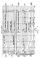
- Fig. 8 shows a comparison between the circuit of Fig. 1 prior art and the circuit of Fig. 4 disclosed using a novel current sink for full scale load transient.
- Fig. 8 compares the output of the LDOs shown in Fig.1 prior art and in Fig. 4 along with the potential at internal nodes between two events of full scale load transient. Trace 88 shows the load current of the full scale load event.
- Traces 80 and 81 show the voltage Vgate
- trace 80 shows the trace of the prior art current sink
- trace 81 shows the trace of the current sink disclosed.
- Traces 82 and 83 show the voltage FST1
- trace 82 shows the trace of the prior art current sink
- trace 83 shows the trace of the current sink disclosed.
- Traces 84 and 85 show the voltage Diffout
- trace 84 shows the trace of the prior art current sink
- trace 85 shows the trace of the current sink disclosed.
- Traces 86 and 87 show the output voltage Vout
- trace 86 shows the trace of the prior art current sink
- trace 87 shows the trace of the current sink disclosed.
- a main point of the current sink disclosed is that the output Diffout of the differential amplifier remains relatively constant in case of the randomly occurring full scale load transient.
- node Fst1 is pulled low to turn off transistor N4.
- Current source 11 tries to pull the voltage Vgate to VDD_PASS.
- the potential difference between Vgate and vcas gets higher than threshold voltage of Pa3 , the current I1 starts to flow from transistor Pa3 to transistor Na2.
- Transistors Na2 and Na3 form a current mirror. Transistor Na3 starts to sink current from VOUT .
- Trace 87 shows an important advantage of the present disclosure, namely the dip of the output voltage is much smaller than the dip of the prior art. This may be of special importance in case the LDO is supplying a chip and a voltage dip such as with prior art is beyond an acceptable voltage swing of the chip. Such a situation would cause a brown-out of the chip which is unacceptable.
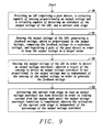
- Fig. 9 illustrates a flowchart of a method to achieve an LDO with a current sink stage, wherein activation of the current sink is independent of a percentage of an output voltage overshoot.
- a first step 90 describes the provision of an LDO comprising a pass device, a circuitry capable of sensing proportionally an output voltage, a circuitry capable of detecting an overshoot of the output voltage of the LDO, and a current sink stage.
- Step 91 shows sensing the output voltage of the LDO, generating a feedback voltage, which is proportional to the output voltage, comparing the feedback voltage to a reference voltage, and regulating a gate of the pass device in order to keep the output voltage on a target value.
- Step 92 illustrates sensing the output voltage of the LDO in order to detect an output voltage overshoot, wherein a result of the sensing to detect an output voltage overshoot is not proportional to the output voltage and is independent of the sensing of the output voltage in order to generate the feedback voltage.
- the final step 93 depicts in case an output voltage overshoot has been detected in order to sinking current from the output node until the output voltage overshoot condition is remediated, wherein the activation of the current sink stage is independent of the percentage of the output voltage overshoot.
Landscapes
- Engineering & Computer Science (AREA)
- Physics & Mathematics (AREA)
- Electromagnetism (AREA)
- General Physics & Mathematics (AREA)
- Radar, Positioning & Navigation (AREA)
- Automation & Control Theory (AREA)
- Microelectronics & Electronic Packaging (AREA)
- Nonlinear Science (AREA)
- Continuous-Control Power Sources That Use Transistors (AREA)
Priority Applications (1)
| Application Number | Priority Date | Filing Date | Title |
|---|---|---|---|
| US14/592,015 US9547323B2 (en) | 2014-06-02 | 2015-01-08 | Current sink stage for LDO |
Applications Claiming Priority (1)
| Application Number | Priority Date | Filing Date | Title |
|---|---|---|---|
| US201462006570P | 2014-06-02 | 2014-06-02 |
Publications (2)
| Publication Number | Publication Date |
|---|---|
| EP2952996A1 true EP2952996A1 (fr) | 2015-12-09 |
| EP2952996B1 EP2952996B1 (fr) | 2019-03-13 |
Family
ID=52338985
Family Applications (1)
| Application Number | Title | Priority Date | Filing Date |
|---|---|---|---|
| EP15150230.9A Active EP2952996B1 (fr) | 2014-06-02 | 2015-01-06 | Étage de collecteur de courant pour LDO |
Country Status (2)
| Country | Link |
|---|---|
| US (1) | US9547323B2 (fr) |
| EP (1) | EP2952996B1 (fr) |
Cited By (3)
| Publication number | Priority date | Publication date | Assignee | Title |
|---|---|---|---|---|
| DE102019202853B3 (de) | 2019-03-01 | 2020-06-18 | Dialog Semiconductor (Uk) Limited | Linearer Spannungsregler und Verfahren zur Spannungsregelung |
| DE102019204594B3 (de) | 2019-04-01 | 2020-06-25 | Dialog Semiconductor (Uk) Limited | Indirekte leckkompensation für mehrstufige verstärker |
| CN111796619A (zh) * | 2020-06-28 | 2020-10-20 | 同济大学 | 一种防止低压差线性稳压器输出电压过冲的电路 |
Families Citing this family (22)
| Publication number | Priority date | Publication date | Assignee | Title |
|---|---|---|---|---|
| US9853533B2 (en) * | 2013-04-25 | 2017-12-26 | Infineon Technologies Austria Ag | Circuit arrangement and method for reproducing a current |
| US9886044B2 (en) * | 2015-08-07 | 2018-02-06 | Mediatek Inc. | Dynamic current sink for stabilizing low dropout linear regulator (LDO) |
| DE102015216928B4 (de) * | 2015-09-03 | 2021-11-04 | Dialog Semiconductor (Uk) Limited | Regler mit Überspannungsklemme und entsprechende Verfahren |
| US9893757B2 (en) * | 2016-02-11 | 2018-02-13 | Texas Instruments Incorporated | Pulse-shaping LDO provides first and second slew-rate increases in amplitude |
| US9846445B2 (en) * | 2016-04-21 | 2017-12-19 | Nxp Usa, Inc. | Voltage supply regulator with overshoot protection |
| US10477626B2 (en) * | 2016-11-23 | 2019-11-12 | Alpha And Omega Semiconductor (Cayman) Ltd. | Hard switching disable for switching power device |
| US10411692B2 (en) | 2016-11-23 | 2019-09-10 | Alpha And Omega Semiconductor Incorporated | Active clamp overvoltage protection for switching power device |
| US10476494B2 (en) | 2017-03-20 | 2019-11-12 | Alpha And Omega Semiconductor (Cayman) Ltd. | Intelligent power modules for resonant converters |
| CN108631617B (zh) * | 2017-03-20 | 2020-06-16 | 万国半导体(开曼)股份有限公司 | 用于开关电源器件的硬开关禁用 |
| EP3514654B1 (fr) | 2018-01-19 | 2020-09-30 | Socionext Inc. | Circuit régulateur de tension |
| KR102452619B1 (ko) | 2018-07-04 | 2022-10-07 | 삼성전자주식회사 | Pvt 변화에 적응성 있는 집적 회로 |
| KR102188844B1 (ko) * | 2019-05-31 | 2020-12-09 | 한양대학교 에리카산학협력단 | 과도 응답이 개선된 로우 드랍아웃 레귤레이터 |
| US10866607B1 (en) | 2019-12-17 | 2020-12-15 | Analog Devices International Unlimited Company | Voltage regulator circuit with correction loop |
| CN111522380B (zh) * | 2020-03-18 | 2024-12-03 | 无锡艾为集成电路技术有限公司 | 线性稳压电路及其静态功耗降低方法、电源管理芯片 |
| DE102020129614B3 (de) * | 2020-11-10 | 2021-11-11 | Infineon Technologies Ag | Spannungsregelschaltkreis und Verfahren zum Betreiben eines Spannungsregelschaltkreises |
| US11561563B2 (en) * | 2020-12-11 | 2023-01-24 | Skyworks Solutions, Inc. | Supply-glitch-tolerant regulator |
| CN112489711B (zh) * | 2020-12-30 | 2021-11-12 | 芯天下技术股份有限公司 | 缓解芯片active模式启动瞬间驱动能力不足的电路 |
| US11644487B2 (en) * | 2021-04-21 | 2023-05-09 | Nxp B.V. | Circuits and methods for tracking minimum voltage at multiple sense points |
| CN113377144A (zh) * | 2021-05-25 | 2021-09-10 | 江苏万邦微电子有限公司 | 一种输出端无过冲电压的线性稳压器电路 |
| US12166417B2 (en) * | 2021-12-17 | 2024-12-10 | Qualcomm Incorporated | Nonlinear current mirror for fast transient and low power regulator |
| CN116088632B (zh) * | 2022-09-05 | 2024-12-06 | 夏芯微电子(上海)有限公司 | Ldo电路、芯片以及终端设备 |
| CN118915867B (zh) * | 2024-07-16 | 2025-09-05 | 同济大学 | 一种含有过冲抑制的低静态电流ldo |
Citations (3)
| Publication number | Priority date | Publication date | Assignee | Title |
|---|---|---|---|---|
| US6333623B1 (en) * | 2000-10-30 | 2001-12-25 | Texas Instruments Incorporated | Complementary follower output stage circuitry and method for low dropout voltage regulator |
| US6949972B1 (en) * | 2004-04-02 | 2005-09-27 | National Semiconductor Corporation | Apparatus and method for current sink circuit |
| EP2648061A1 (fr) * | 2012-04-06 | 2013-10-09 | Dialog Semiconductor GmbH | Compensation de fuite pour transistor de sortie d'un régulateur LDO à puissance ultra faible |
Family Cites Families (8)
| Publication number | Priority date | Publication date | Assignee | Title |
|---|---|---|---|---|
| US5637992A (en) * | 1995-05-31 | 1997-06-10 | Sgs-Thomson Microelectronics, Inc. | Voltage regulator with load pole stabilization |
| US6977491B1 (en) | 2003-10-06 | 2005-12-20 | National Semiconductor Corporation | Current limiting voltage regulation circuit |
| US7602162B2 (en) | 2005-11-29 | 2009-10-13 | Stmicroelectronics Pvt. Ltd. | Voltage regulator with over-current protection |
| TW200820562A (en) * | 2006-10-20 | 2008-05-01 | Holtek Semiconductor Inc | Voltage regulator with accelerated output recovery |
| KR100804643B1 (ko) | 2006-11-30 | 2008-02-20 | 삼성전자주식회사 | 전압 레귤레이터, 이를 포함하는 디지털 앰프 및 전압 조절방법 |
| US7893671B2 (en) | 2007-03-12 | 2011-02-22 | Texas Instruments Incorporated | Regulator with improved load regulation |
| DE102007059498A1 (de) | 2007-12-11 | 2009-06-18 | Texas Instruments Deutschland Gmbh | Linearer Spannungsregler mit präziser Detektion einer offenen Last |
| US9651967B2 (en) | 2011-11-09 | 2017-05-16 | Nxp B.V. | Power supply with integrated voltage clamp and current sink |
-
2015
- 2015-01-06 EP EP15150230.9A patent/EP2952996B1/fr active Active
- 2015-01-08 US US14/592,015 patent/US9547323B2/en active Active
Patent Citations (3)
| Publication number | Priority date | Publication date | Assignee | Title |
|---|---|---|---|---|
| US6333623B1 (en) * | 2000-10-30 | 2001-12-25 | Texas Instruments Incorporated | Complementary follower output stage circuitry and method for low dropout voltage regulator |
| US6949972B1 (en) * | 2004-04-02 | 2005-09-27 | National Semiconductor Corporation | Apparatus and method for current sink circuit |
| EP2648061A1 (fr) * | 2012-04-06 | 2013-10-09 | Dialog Semiconductor GmbH | Compensation de fuite pour transistor de sortie d'un régulateur LDO à puissance ultra faible |
Non-Patent Citations (1)
| Title |
|---|
| GUTIERREZ L ET AL: "A Current-Efficient, Low-Dropout Regulator with Improved Load Regulation", MICROELECTRONICS AND ELECTRON DEVICES, 2009. WMED 2009. IEEE WORKSHOP ON, IEEE, PISCATAWAY, NJ, USA, 3 April 2009 (2009-04-03), pages 1 - 4, XP031449795, ISBN: 978-1-4244-3551-7 * |
Cited By (5)
| Publication number | Priority date | Publication date | Assignee | Title |
|---|---|---|---|---|
| DE102019202853B3 (de) | 2019-03-01 | 2020-06-18 | Dialog Semiconductor (Uk) Limited | Linearer Spannungsregler und Verfahren zur Spannungsregelung |
| US11625055B2 (en) | 2019-03-01 | 2023-04-11 | Dialog Semiconductor (Uk) Limited | Programmable two-way fast DVC control circuit |
| DE102019204594B3 (de) | 2019-04-01 | 2020-06-25 | Dialog Semiconductor (Uk) Limited | Indirekte leckkompensation für mehrstufige verstärker |
| US11099590B2 (en) | 2019-04-01 | 2021-08-24 | Dialog Semiconductor (Uk) Limited | Indirect leakage compensation for multi-stage amplifiers |
| CN111796619A (zh) * | 2020-06-28 | 2020-10-20 | 同济大学 | 一种防止低压差线性稳压器输出电压过冲的电路 |
Also Published As
| Publication number | Publication date |
|---|---|
| US20150346750A1 (en) | 2015-12-03 |
| US9547323B2 (en) | 2017-01-17 |
| EP2952996B1 (fr) | 2019-03-13 |
Similar Documents
| Publication | Publication Date | Title |
|---|---|---|
| US9547323B2 (en) | Current sink stage for LDO | |
| EP2701030B1 (fr) | Régulateur à faible chute de tension avec une référence de tension flottante | |
| US9846445B2 (en) | Voltage supply regulator with overshoot protection | |
| US8575903B2 (en) | Voltage regulator that can operate with or without an external power transistor | |
| US11435768B2 (en) | N-channel input pair voltage regulator with soft start and current limitation circuitry | |
| US8508199B2 (en) | Current limitation for LDO | |
| CN116301145B (zh) | 一种低压差线性稳压器及其控制电路、芯片和电子设备 | |
| US11281244B2 (en) | Output current limiter for a linear regulator | |
| US10382030B2 (en) | Apparatus having process, voltage and temperature-independent line transient management | |
| US20180329440A1 (en) | Voltage Regulator and Method for Providing an Output Voltage with Reduced Voltage Ripple | |
| US7907003B2 (en) | Method for improving power-supply rejection | |
| CN102455730A (zh) | 稳压器用半导体集成电路 | |
| KR102187403B1 (ko) | 볼티지 레귤레이터 | |
| US9606556B2 (en) | Semiconductor integrated circuit for regulator | |
| US7737676B2 (en) | Series regulator circuit | |
| US9323265B2 (en) | Voltage regulator output overvoltage compensation | |
| CN111488028A (zh) | 形成半导体器件的方法 | |
| JP5895369B2 (ja) | レギュレータ用半導体集積回路 | |
| JP5793979B2 (ja) | レギュレータ用半導体集積回路 | |
| US10969809B2 (en) | Dual input LDO voltage regulator | |
| US10216207B2 (en) | Overvoltage clamp in regulators | |
| US10802517B1 (en) | Multi-mode voltage regulator | |
| US9946276B2 (en) | Voltage regulators with current reduction mode | |
| US10291163B2 (en) | Cascode structure for linear regulators and clamps | |
| US10969810B2 (en) | Voltage regulator with virtual zero quiescent current |
Legal Events
| Date | Code | Title | Description |
|---|---|---|---|
| PUAI | Public reference made under article 153(3) epc to a published international application that has entered the european phase |
Free format text: ORIGINAL CODE: 0009012 |
|
| AK | Designated contracting states |
Kind code of ref document: A1 Designated state(s): AL AT BE BG CH CY CZ DE DK EE ES FI FR GB GR HR HU IE IS IT LI LT LU LV MC MK MT NL NO PL PT RO RS SE SI SK SM TR |
|
| AX | Request for extension of the european patent |
Extension state: BA ME |
|
| RAP1 | Party data changed (applicant data changed or rights of an application transferred) |
Owner name: DIALOG SEMICONDUCTOR (UK) LIMITED |
|
| 17P | Request for examination filed |
Effective date: 20160324 |
|
| RBV | Designated contracting states (corrected) |
Designated state(s): AL AT BE BG CH CY CZ DE DK EE ES FI FR GB GR HR HU IE IS IT LI LT LU LV MC MK MT NL NO PL PT RO RS SE SI SK SM TR |
|
| RIC1 | Information provided on ipc code assigned before grant |
Ipc: G05F 3/26 20060101ALI20180516BHEP Ipc: G05F 1/56 20060101ALI20180516BHEP Ipc: G05F 1/575 20060101AFI20180516BHEP |
|
| GRAP | Despatch of communication of intention to grant a patent |
Free format text: ORIGINAL CODE: EPIDOSNIGR1 |
|
| STAA | Information on the status of an ep patent application or granted ep patent |
Free format text: STATUS: GRANT OF PATENT IS INTENDED |
|
| INTG | Intention to grant announced |
Effective date: 20180719 |
|
| GRAS | Grant fee paid |
Free format text: ORIGINAL CODE: EPIDOSNIGR3 |
|
| GRAA | (expected) grant |
Free format text: ORIGINAL CODE: 0009210 |
|
| STAA | Information on the status of an ep patent application or granted ep patent |
Free format text: STATUS: THE PATENT HAS BEEN GRANTED |
|
| AK | Designated contracting states |
Kind code of ref document: B1 Designated state(s): AL AT BE BG CH CY CZ DE DK EE ES FI FR GB GR HR HU IE IS IT LI LT LU LV MC MK MT NL NO PL PT RO RS SE SI SK SM TR |
|
| REG | Reference to a national code |
Ref country code: GB Ref legal event code: FG4D |
|
| REG | Reference to a national code |
Ref country code: CH Ref legal event code: EP Ref country code: AT Ref legal event code: REF Ref document number: 1108559 Country of ref document: AT Kind code of ref document: T Effective date: 20190315 |
|
| REG | Reference to a national code |
Ref country code: IE Ref legal event code: FG4D |
|
| REG | Reference to a national code |
Ref country code: DE Ref legal event code: R096 Ref document number: 602015026144 Country of ref document: DE |
|
| REG | Reference to a national code |
Ref country code: NL Ref legal event code: MP Effective date: 20190313 |
|
| REG | Reference to a national code |
Ref country code: LT Ref legal event code: MG4D |
|
| PG25 | Lapsed in a contracting state [announced via postgrant information from national office to epo] |
Ref country code: FI Free format text: LAPSE BECAUSE OF FAILURE TO SUBMIT A TRANSLATION OF THE DESCRIPTION OR TO PAY THE FEE WITHIN THE PRESCRIBED TIME-LIMIT Effective date: 20190313 Ref country code: LT Free format text: LAPSE BECAUSE OF FAILURE TO SUBMIT A TRANSLATION OF THE DESCRIPTION OR TO PAY THE FEE WITHIN THE PRESCRIBED TIME-LIMIT Effective date: 20190313 Ref country code: NO Free format text: LAPSE BECAUSE OF FAILURE TO SUBMIT A TRANSLATION OF THE DESCRIPTION OR TO PAY THE FEE WITHIN THE PRESCRIBED TIME-LIMIT Effective date: 20190613 Ref country code: SE Free format text: LAPSE BECAUSE OF FAILURE TO SUBMIT A TRANSLATION OF THE DESCRIPTION OR TO PAY THE FEE WITHIN THE PRESCRIBED TIME-LIMIT Effective date: 20190313 |
|
| PG25 | Lapsed in a contracting state [announced via postgrant information from national office to epo] |
Ref country code: NL Free format text: LAPSE BECAUSE OF FAILURE TO SUBMIT A TRANSLATION OF THE DESCRIPTION OR TO PAY THE FEE WITHIN THE PRESCRIBED TIME-LIMIT Effective date: 20190313 Ref country code: LV Free format text: LAPSE BECAUSE OF FAILURE TO SUBMIT A TRANSLATION OF THE DESCRIPTION OR TO PAY THE FEE WITHIN THE PRESCRIBED TIME-LIMIT Effective date: 20190313 Ref country code: HR Free format text: LAPSE BECAUSE OF FAILURE TO SUBMIT A TRANSLATION OF THE DESCRIPTION OR TO PAY THE FEE WITHIN THE PRESCRIBED TIME-LIMIT Effective date: 20190313 Ref country code: GR Free format text: LAPSE BECAUSE OF FAILURE TO SUBMIT A TRANSLATION OF THE DESCRIPTION OR TO PAY THE FEE WITHIN THE PRESCRIBED TIME-LIMIT Effective date: 20190614 Ref country code: RS Free format text: LAPSE BECAUSE OF FAILURE TO SUBMIT A TRANSLATION OF THE DESCRIPTION OR TO PAY THE FEE WITHIN THE PRESCRIBED TIME-LIMIT Effective date: 20190313 Ref country code: BG Free format text: LAPSE BECAUSE OF FAILURE TO SUBMIT A TRANSLATION OF THE DESCRIPTION OR TO PAY THE FEE WITHIN THE PRESCRIBED TIME-LIMIT Effective date: 20190613 |
|
| REG | Reference to a national code |
Ref country code: AT Ref legal event code: MK05 Ref document number: 1108559 Country of ref document: AT Kind code of ref document: T Effective date: 20190313 |
|
| PG25 | Lapsed in a contracting state [announced via postgrant information from national office to epo] |
Ref country code: EE Free format text: LAPSE BECAUSE OF FAILURE TO SUBMIT A TRANSLATION OF THE DESCRIPTION OR TO PAY THE FEE WITHIN THE PRESCRIBED TIME-LIMIT Effective date: 20190313 Ref country code: IT Free format text: LAPSE BECAUSE OF FAILURE TO SUBMIT A TRANSLATION OF THE DESCRIPTION OR TO PAY THE FEE WITHIN THE PRESCRIBED TIME-LIMIT Effective date: 20190313 Ref country code: RO Free format text: LAPSE BECAUSE OF FAILURE TO SUBMIT A TRANSLATION OF THE DESCRIPTION OR TO PAY THE FEE WITHIN THE PRESCRIBED TIME-LIMIT Effective date: 20190313 Ref country code: CZ Free format text: LAPSE BECAUSE OF FAILURE TO SUBMIT A TRANSLATION OF THE DESCRIPTION OR TO PAY THE FEE WITHIN THE PRESCRIBED TIME-LIMIT Effective date: 20190313 Ref country code: ES Free format text: LAPSE BECAUSE OF FAILURE TO SUBMIT A TRANSLATION OF THE DESCRIPTION OR TO PAY THE FEE WITHIN THE PRESCRIBED TIME-LIMIT Effective date: 20190313 Ref country code: PT Free format text: LAPSE BECAUSE OF FAILURE TO SUBMIT A TRANSLATION OF THE DESCRIPTION OR TO PAY THE FEE WITHIN THE PRESCRIBED TIME-LIMIT Effective date: 20190713 Ref country code: SK Free format text: LAPSE BECAUSE OF FAILURE TO SUBMIT A TRANSLATION OF THE DESCRIPTION OR TO PAY THE FEE WITHIN THE PRESCRIBED TIME-LIMIT Effective date: 20190313 Ref country code: AL Free format text: LAPSE BECAUSE OF FAILURE TO SUBMIT A TRANSLATION OF THE DESCRIPTION OR TO PAY THE FEE WITHIN THE PRESCRIBED TIME-LIMIT Effective date: 20190313 |
|
| PG25 | Lapsed in a contracting state [announced via postgrant information from national office to epo] |
Ref country code: PL Free format text: LAPSE BECAUSE OF FAILURE TO SUBMIT A TRANSLATION OF THE DESCRIPTION OR TO PAY THE FEE WITHIN THE PRESCRIBED TIME-LIMIT Effective date: 20190313 Ref country code: SM Free format text: LAPSE BECAUSE OF FAILURE TO SUBMIT A TRANSLATION OF THE DESCRIPTION OR TO PAY THE FEE WITHIN THE PRESCRIBED TIME-LIMIT Effective date: 20190313 |
|
| REG | Reference to a national code |
Ref country code: DE Ref legal event code: R097 Ref document number: 602015026144 Country of ref document: DE |
|
| PG25 | Lapsed in a contracting state [announced via postgrant information from national office to epo] |
Ref country code: AT Free format text: LAPSE BECAUSE OF FAILURE TO SUBMIT A TRANSLATION OF THE DESCRIPTION OR TO PAY THE FEE WITHIN THE PRESCRIBED TIME-LIMIT Effective date: 20190313 Ref country code: IS Free format text: LAPSE BECAUSE OF FAILURE TO SUBMIT A TRANSLATION OF THE DESCRIPTION OR TO PAY THE FEE WITHIN THE PRESCRIBED TIME-LIMIT Effective date: 20190713 |
|
| PLBE | No opposition filed within time limit |
Free format text: ORIGINAL CODE: 0009261 |
|
| STAA | Information on the status of an ep patent application or granted ep patent |
Free format text: STATUS: NO OPPOSITION FILED WITHIN TIME LIMIT |
|
| PG25 | Lapsed in a contracting state [announced via postgrant information from national office to epo] |
Ref country code: DK Free format text: LAPSE BECAUSE OF FAILURE TO SUBMIT A TRANSLATION OF THE DESCRIPTION OR TO PAY THE FEE WITHIN THE PRESCRIBED TIME-LIMIT Effective date: 20190313 |
|
| 26N | No opposition filed |
Effective date: 20191216 |
|
| PG25 | Lapsed in a contracting state [announced via postgrant information from national office to epo] |
Ref country code: SI Free format text: LAPSE BECAUSE OF FAILURE TO SUBMIT A TRANSLATION OF THE DESCRIPTION OR TO PAY THE FEE WITHIN THE PRESCRIBED TIME-LIMIT Effective date: 20190313 |
|
| PG25 | Lapsed in a contracting state [announced via postgrant information from national office to epo] |
Ref country code: TR Free format text: LAPSE BECAUSE OF FAILURE TO SUBMIT A TRANSLATION OF THE DESCRIPTION OR TO PAY THE FEE WITHIN THE PRESCRIBED TIME-LIMIT Effective date: 20190313 |
|
| PG25 | Lapsed in a contracting state [announced via postgrant information from national office to epo] |
Ref country code: MC Free format text: LAPSE BECAUSE OF FAILURE TO SUBMIT A TRANSLATION OF THE DESCRIPTION OR TO PAY THE FEE WITHIN THE PRESCRIBED TIME-LIMIT Effective date: 20190313 |
|
| REG | Reference to a national code |
Ref country code: CH Ref legal event code: PL |
|
| REG | Reference to a national code |
Ref country code: BE Ref legal event code: MM Effective date: 20200131 |
|
| PG25 | Lapsed in a contracting state [announced via postgrant information from national office to epo] |
Ref country code: FR Free format text: LAPSE BECAUSE OF NON-PAYMENT OF DUE FEES Effective date: 20200131 Ref country code: LU Free format text: LAPSE BECAUSE OF NON-PAYMENT OF DUE FEES Effective date: 20200106 |
|
| PG25 | Lapsed in a contracting state [announced via postgrant information from national office to epo] |
Ref country code: BE Free format text: LAPSE BECAUSE OF NON-PAYMENT OF DUE FEES Effective date: 20200131 Ref country code: LI Free format text: LAPSE BECAUSE OF NON-PAYMENT OF DUE FEES Effective date: 20200131 Ref country code: CH Free format text: LAPSE BECAUSE OF NON-PAYMENT OF DUE FEES Effective date: 20200131 |
|
| PG25 | Lapsed in a contracting state [announced via postgrant information from national office to epo] |
Ref country code: IE Free format text: LAPSE BECAUSE OF NON-PAYMENT OF DUE FEES Effective date: 20200106 |
|
| PG25 | Lapsed in a contracting state [announced via postgrant information from national office to epo] |
Ref country code: MT Free format text: LAPSE BECAUSE OF FAILURE TO SUBMIT A TRANSLATION OF THE DESCRIPTION OR TO PAY THE FEE WITHIN THE PRESCRIBED TIME-LIMIT Effective date: 20190313 Ref country code: CY Free format text: LAPSE BECAUSE OF FAILURE TO SUBMIT A TRANSLATION OF THE DESCRIPTION OR TO PAY THE FEE WITHIN THE PRESCRIBED TIME-LIMIT Effective date: 20190313 |
|
| PG25 | Lapsed in a contracting state [announced via postgrant information from national office to epo] |
Ref country code: MK Free format text: LAPSE BECAUSE OF FAILURE TO SUBMIT A TRANSLATION OF THE DESCRIPTION OR TO PAY THE FEE WITHIN THE PRESCRIBED TIME-LIMIT Effective date: 20190313 |
|
| PGFP | Annual fee paid to national office [announced via postgrant information from national office to epo] |
Ref country code: GB Payment date: 20260113 Year of fee payment: 12 |
|
| PGFP | Annual fee paid to national office [announced via postgrant information from national office to epo] |
Ref country code: DE Payment date: 20260108 Year of fee payment: 12 |