EP2953246B1 - Identification de la dégradation d'un condensateur de filtre au moyen d'une tension calculée et mesurée - Google Patents
Identification de la dégradation d'un condensateur de filtre au moyen d'une tension calculée et mesurée Download PDFInfo
- Publication number
- EP2953246B1 EP2953246B1 EP15170476.4A EP15170476A EP2953246B1 EP 2953246 B1 EP2953246 B1 EP 2953246B1 EP 15170476 A EP15170476 A EP 15170476A EP 2953246 B1 EP2953246 B1 EP 2953246B1
- Authority
- EP
- European Patent Office
- Prior art keywords
- value
- filter circuit
- filter
- voltage
- computing
- Prior art date
- Legal status (The legal status is an assumption and is not a legal conclusion. Google has not performed a legal analysis and makes no representation as to the accuracy of the status listed.)
- Active
Links
Images


Classifications
-
- G—PHYSICS
- G01—MEASURING; TESTING
- G01R—MEASURING ELECTRIC VARIABLES; MEASURING MAGNETIC VARIABLES
- G01R31/00—Arrangements for testing electric properties; Arrangements for locating electric faults; Arrangements for electrical testing characterised by what is being tested not provided for elsewhere
- G01R31/40—Testing power supplies
- G01R31/42—AC power supplies
-
- G—PHYSICS
- G01—MEASURING; TESTING
- G01R—MEASURING ELECTRIC VARIABLES; MEASURING MAGNETIC VARIABLES
- G01R19/00—Arrangements for measuring currents or voltages or for indicating presence or sign thereof
- G01R19/0084—Measuring voltage only
-
- G—PHYSICS
- G01—MEASURING; TESTING
- G01R—MEASURING ELECTRIC VARIABLES; MEASURING MAGNETIC VARIABLES
- G01R27/00—Arrangements for measuring resistance, reactance, impedance, or electric characteristics derived therefrom
- G01R27/02—Measuring real or complex resistance, reactance, impedance, or other two-pole characteristics derived therefrom, e.g. time constant
- G01R27/26—Measuring inductance or capacitance; Measuring quality factor, e.g. by using the resonance method; Measuring loss factor; Measuring dielectric constants ; Measuring impedance or related variables
- G01R27/2688—Measuring quality factor or dielectric loss, e.g. loss angle, or power factor
-
- G—PHYSICS
- G01—MEASURING; TESTING
- G01R—MEASURING ELECTRIC VARIABLES; MEASURING MAGNETIC VARIABLES
- G01R31/00—Arrangements for testing electric properties; Arrangements for locating electric faults; Arrangements for electrical testing characterised by what is being tested not provided for elsewhere
- G01R31/34—Testing dynamo-electric machines
-
- G—PHYSICS
- G01—MEASURING; TESTING
- G01R—MEASURING ELECTRIC VARIABLES; MEASURING MAGNETIC VARIABLES
- G01R31/00—Arrangements for testing electric properties; Arrangements for locating electric faults; Arrangements for electrical testing characterised by what is being tested not provided for elsewhere
- G01R31/50—Testing of electric apparatus, lines, cables or components for short-circuits, continuity, leakage current or incorrect line connections
- G01R31/64—Testing of capacitors
-
- H—ELECTRICITY
- H02—GENERATION; CONVERSION OR DISTRIBUTION OF ELECTRIC POWER
- H02M—APPARATUS FOR CONVERSION BETWEEN AC AND AC, BETWEEN AC AND DC, OR BETWEEN DC AND DC, AND FOR USE WITH MAINS OR SIMILAR POWER SUPPLY SYSTEMS; CONVERSION OF DC OR AC INPUT POWER INTO SURGE OUTPUT POWER; CONTROL OR REGULATION THEREOF
- H02M1/00—Details of apparatus for conversion
- H02M1/12—Arrangements for reducing harmonics from AC input or output
- H02M1/126—Arrangements for reducing harmonics from AC input or output using passive filters
-
- G—PHYSICS
- G01—MEASURING; TESTING
- G01R—MEASURING ELECTRIC VARIABLES; MEASURING MAGNETIC VARIABLES
- G01R19/00—Arrangements for measuring currents or voltages or for indicating presence or sign thereof
- G01R19/0092—Measuring current only
-
- G—PHYSICS
- G01—MEASURING; TESTING
- G01R—MEASURING ELECTRIC VARIABLES; MEASURING MAGNETIC VARIABLES
- G01R31/00—Arrangements for testing electric properties; Arrangements for locating electric faults; Arrangements for electrical testing characterised by what is being tested not provided for elsewhere
- G01R31/50—Testing of electric apparatus, lines, cables or components for short-circuits, continuity, leakage current or incorrect line connections
Definitions
- the subject matter disclosed herein relates to power conversion, and more specifically to apparatus and techniques for detection of degraded filter circuit capacitor components.
- a method for detecting filter circuit capacitor degradation including measuring filter circuit currents and voltages, computing an expected DC equivalent voltage value at least partially according to the measured currents and a filter capacitor impedance value, and computing a measured DC equivalent voltage value at least partially according to the filter circuit voltages.
- a voltage change value is computed representing deviation of measured and expected DC equivalent voltage values, and a filter capacitor degradation condition is selectively detected or identified at least partially according to the voltage change value.
- a power conversion system including a filter circuit, a measurement circuit configured to measure filter circuit branch currents and filter circuit voltages, and at least one processor programmed to compute an expected DC equivalent voltage value at least partially according to the filter circuit branch currents and a filter capacitor impedance value, and to compute a present measured DC equivalent voltage value at least partially according to the filter circuit voltages.
- the processor is further programmed to compute a voltage change value representing a voltage deviation of a measured DC equivalent voltage value and an expected DC equivalent voltage value, and to selectively identify a filter capacitor degradation condition in the filter circuit at least partially according to the voltage change value.
- Motor drives and other power converters operate using power from AC power sources.
- An input filter circuit is often provided to reduce switching noise associated with operation of the power converter, and particularly to control total harmonic distortion (THD) generated by high frequency operation of certain active front end rectifiers.
- TDD total harmonic distortion
- inductor - capacitor (L-C) or inductance - capacitance - inductance (L-C-L) input filter circuitry may be associated with each AC input phase to control the harmonic content of a connected power grid.
- capacitors in such filter circuits may be subject to damage or degradation, and such degradation may be costly in terms of replacement component costs, labor for inspection and replacement, as well as downtime for the power converter and any associated machinery to manually identify one or more degraded capacitors.
- capacitor degradation may not be identifiable through simple visual inspection by service personnel. Fuses may be placed in line with the filter circuit capacitors, but the fuses may not open quickly enough to prevent capacitor degradation or may open frequently in normal operation with healthy capacitors, leading to excessive system downtime and further costs for inspection and system verification.
- the filter capacitors may degrade to a high resistance short whereby fuses may not protect the motor drive or other power conversion system components, and the failure modes of the filter capacitors often go unobserved until significant degradation has occurred.
- the present disclosure provides filter capacitor degradation identification solutions that find particular utility in connection with active front end power converters and other power converters, as well as in other filter circuit applications.
- Exemplary methods and apparatus are hereinafter disclosed for active front end power converter filter capacitor degradation detection in which filter circuit branch currents and voltages are measured, with expected and measured DC equivalent voltage values being computed and compared to selectively identify capacitor degradation conditions in the filter circuit.
- the disclosure thus presents a significant advance since fuses are not required and the onset of degradation can be assessed prior to system damage.
- the detected degradation condition can be used, in turn, to provide a system alert or warning and/or to shut down the power converter in certain non-limiting applications.
- the disclosed concepts find utility in association with active front end motor drives as well as other forms of power converters.
- the disclosed concepts can be employed in power converters having any number of input phases in which a filter includes a capacitor circuit or capacitor bank.
- the disclosed techniques and apparatus advantageously facilitate identification of potential degradation of individual filter capacitors or groups thereof, and a determination can be made as to whether one or more of these components are degrading in certain embodiments.
- the degradation detection moreover, can be used to initiate any appropriate remedial or reporting action.
- the present disclosure avoids the over inclusive or under inclusive nature of protective fuse-based solutions, and also advantageously facilitates early identification of the onset of component degradation filter capacitors. This, in turn, can facilitate reduction in system downtime and reduce or mitigate maintenance costs associated with operation of a motor drive or other power converter.
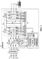
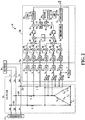
- Figs. 1 and 2 illustrate an exemplary active front end motor drive 10 with a delta-connected filter circuit 20, where Fig. 2 shows details of an exemplary filter capacitor degradation detection system 70 according to one embodiment.
- the illustrated drive 10 is a voltage source converter (VSC) having an intermediate DC link circuit 40 with one or more bus capacitors (Cdc).
- VSC voltage source converter
- Cdc bus capacitors
- the motor drive 10 includes a three phase AC input 4 receiving input power from a three-phase source 2 via an optional transformer 3. As best seen in Fig.
- the drive 10 includes a rectifier 30, an intermediate DC link circuit 40 and an output inverter 50 providing variable frequency, variable amplitude AC output power to drive a motor load 6.
- the various disclosed concepts can be employed in other forms of power converters, whether providing an AC output or a DC output to drive a motor or other type of load 6.
- the drive input 4 in the illustrated non-limiting example has three input phase terminals which are connected through an LCL input filter circuit 20 to the AC input of the switching (e.g., active front end) rectifier 30.
- L-C-L filter having two inductors in each series circuit path between the input 4 and the rectifier 30, the various concepts of the present disclosure can be employed in connection with other filter circuit topologies including without limitation L-C filters, C-L filters, etc.
- the filter circuit 20 includes a set or bank of three capacitors C ab , C bc and C ca connected in a delta configuration.
- the capacitor bank of the filter circuit 20 is configured in a "Y" configuration (e.g., capacitors C a , C b and C c in Fig. 6 below).
- the individual capacitors of the filter circuit 20 can be constructed using a single capacitor component, or may be individually constructed as series and/or parallel combinations of multiple capacitive components in various embodiments, and are hereinafter collectively termed "filter capacitors".
- filter capacitors For example, Fig.
- FIG. 3 illustrates a delta-connected filter capacitor bank embodiment with three parallel-connected capacitor components in each line-line branch forming the filter capacitors C ab , C bc and C ca of the delta-connected filter 20.
- certain embodiments of the filter circuit 20 may also include discharge resistors (not shown) individually connected in parallel across a corresponding one of the filter capacitors C ab , C bc and C ca (in either or both of the delta or Y configurations) providing discharge paths with respect to filter capacitor voltages.
- damping resistors can be provided in certain filter circuit embodiments, in series with the filter capacitors.
- the capacitor degradation detection and identification methods and apparatus of the present disclosure can separately or in combination be employed for detecting degradation of trap filter or output filter capacitor components, such as in an LC or LCL filter circuit (not shown) connected between the inverter AC outputs and a driven load 6, including one or more inductors connected in series between the inverter 50 and the load 6 and a bank of capacitors individually connected to at least one of the AC lines, whether in a delta configuration or in a Y configuration.
- the switching rectifier 30 includes switching devices S1-S6 individually coupled between a corresponding one of the AC input phases (u, v, w) and a corresponding DC bus terminal (+ or -) of the DC link circuit 40.
- a drive controller 60 includes a rectifier switching controller 62 that provides rectifier switching control signal 62a to the rectifier switches S1-S6 to cause the rectifier 30 to convert received three-phase AC input power to provide a DC voltage Vdc across a DC bus capacitance Cdc of the link circuit 40 using any suitable pulse width modulation (PWM) technique.
- PWM pulse width modulation
- Other embodiments are possible, for example, using passive rectifier circuitry 30.
- the drive inverter 50 receives DC input power from the link circuit 40 and includes inverter switches S7-S12 individually coupled between one of the positive or negative DC bus terminals and a corresponding output phase connected to the motor load 6.
- the inverter switches S7-S12 are operated according to inverter switching control signals 66a provided by an inverter switching component 66 of the drive controller 60, which generates the signals 66a according to any suitable pulse width modulation technique to convert DC power from the link circuit 40 to provide variable frequency, variable amplitude AC output power to the motor load 6.
- the switching rectifier 30 and the inverter 50 may employ any suitable form of switching devices S1-S12 including without limitation insulated gate bipolar transistors (IGBTs), silicon controlled rectifiers (SCRs), gate turn-off thyristors (GTOs), integrated gate commutated thyristors (IGCTs), etc.
- the controller 60 can be any suitable hardware, processor-executed software, processor-executed firmware, programmable logic, analog circuitry, etc. or combinations thereof which provides control signals 62a, 66a for operating the rectifier 30 and the inverter 50, and may implement other functionality associated with operation of the motor drive 10.
- While the illustrated embodiment includes a switching inverter 50 and associated controller 66, other power converter configurations or embodiments are possible in which the DC power provided at the bus circuit 40 is provided as an output, wherein the inverter 50 and inverter switching controller 66 may be omitted.
- the LCL filter circuit 20 in Figs. 1 and 2 includes three series circuits individually connected between the power converter input 4 and the corresponding phase of the rectifier AC input.
- Each series circuit includes a pair of series-connected filter inductors, with the first circuit including inductor La connected between the first power converter input terminal and a first intermediate node "a”, as well as a second filter inductor Lu connected between the intermediate node a and a first rectifier AC input node "u".
- the second series circuit includes a first inductor Lb connected between the second motor drive input and a second intermediate node “b” and a second inductor Lv connected between the node b and the second rectifier input "v", as well as a third series circuit with first and second inductors Lc and Lw joined by a third intermediate node "c".
- the filter circuit 20 includes three capacitor circuit branches 22a, 22b and 22c respectively connecting the nodes a, b and c to a delta configuration of the three filter capacitors C ab , C bc and C ca . In the illustrated delta-connected capacitor circuit or capacitor bank, each filter capacitor is connected to two of the capacitor circuit branches 22 (e.g., line-to-line) as shown.
- a CL filter circuit 20 is provided (not shown) for interfacing the motor drive 10 with the power source 2, directly or through a transformer 3, for instance, with the first filter inductors La, Lb and Lc omitted due to the inductance of the secondary windings of the transformer 3, and with the input terminals 4 and the capacitor circuit branches 22a, 22b and 22c being connected directly to the inductors Lu, Lv and Lw at the nodes a, b and c, respectively.
- a degradation detection system 70 is operatively coupled with the filter circuit 20, including measurement circuitry 74a ( Fig. 2 ) to sense or otherwise measure line-to-line voltages V ab , V bc and V ca across the filter capacitors C ab , C bc and C ca , for example, by sensing the voltages at the branch circuits 22 as illustrated.
- the measurement circuitry 74a may include, or couple to, current sensors coupled to the branch circuits 22 to sense the filter circuit branch currents I a , I b and I c flowing in the associated capacitor circuit branches 22a, 22b and 22c, respectively.
- the degradation detection system 70 is depicted in Figs. 1 and 2 , including a microprocessor element 71 along with an electronic memory 73, comparator circuitry 72, a voltage computation component 74 and one or more thresholds 76.
- the degradation detection system 70 can be any suitable hardware, processor-executed software, processor-executed firmware, programmable logic, analog circuitry, etc. or combinations thereof which provides the described capacitor degradation detection functionality, which may include multiplication, summation, filtering, squaring, and square root functional computations and/or threshold comparison functionality in certain embodiments as set forth hereinafter, and the system 70 may be operative using one or more processor elements 71 executing computer executable instructions stored in an electronic memory 73 of the system 70.
- the degradation detection system 70 may include one or more components, some of which may be implemented as software and/or firmware components in execution, programmable logic, etc., including digital current computation component 74b with analog-to-digital conversion 82, multiplication functions 84, 86 and 91, summation functions 85 and 90 (including subtraction), square root functions 88, an optional delay function 89, a moving average function 94, an absolute value function 96, comparators 72, and the memory 73 in certain embodiments may store one or more threshold values 76.
- digital current computation component 74b with analog-to-digital conversion 82 multiplication functions 84, 86 and 91, summation functions 85 and 90 (including subtraction), square root functions 88, an optional delay function 89, a moving average function 94, an absolute value function 96, comparators 72, and the memory 73 in certain embodiments may store one or more threshold values 76.
- the degradation detection system 70 in certain implementations provides one or more output signals or values 78 to identify a detected filter capacitor degradation condition in the filter circuit 20, which may include an indication that at least one capacitor C ab , C bc and/or C ca of the filter circuit 20 is over capacitance or under capacitance or otherwise out of tolerance.
- the degradation detection or identification signal 78 may be provided to the motor drive controller 60 to initiate one or more actions, such as shutting down the motor drive 10 and/or providing an alert or warning signal or other indication, for instance, to a user interface associated with the motor drive 10 and/or to a connected network (not shown).
- the illustrated example includes measurement circuitry 74a as well as digital processing circuitry or processor-implemented logic 74b for DC equivalent voltage computation, including a comparator function 72 to compare voltage change values 97 with one or more thresholds 76 for selective provision of one or more filter capacitor degradation condition signals or values 78, providing a non-limiting embodiment of the voltage computation component 74 in Fig. 1 .
- a comparator function 72 to compare voltage change values 97 with one or more thresholds 76 for selective provision of one or more filter capacitor degradation condition signals or values 78, providing a non-limiting embodiment of the voltage computation component 74 in Fig. 1 .
- the system 70 includes analog measurement circuitry 74a with differential amplifiers 80 measuring filter circuit line-to-line voltages V ab , V bc and V ca , as well as analog low pass filter (LPF) circuits 81 operative to low pass filter the measured filter circuit voltages V ab , V bc and V ca .
- LPF low pass filter
- current sensor inputs i a , i b and i c are provided to corresponding low pass filter circuits 81 for filtering measured filter circuit branch currents sensed along the capacitor circuit branches 22a, 22b and 22c, respectively.
- the low pass filter circuits 81 have a cutoff frequency above the operating frequency of the system 10.
- a cutoff frequency of approximately 200 Hz can be used for a motor drive system 10 operating from a 50 Hz or 60 Hz supply in one non-limiting embodiment.
- the low pass filters 81 may be implemented as analog filter circuits in one embodiment, or low pass filtering may be implemented following the analog-to-digital converters 82, for example, using infinite impulse response (IIR) filters 81 having a low pass filter cutoff frequency of around 200 Hz in one non-limiting embodiment.
- IIR infinite impulse response
- Analog-to-digital converters 82 are provided in the example of Fig. 2 for concurrent sampling and conversion of the measured filter circuit voltages V ab , V bc and V ca and filter branch currents i a , i b and i c , with the converters 82 providing converted digital values V ab , V bc and V ca representing the line-to-line voltages provided to the delta-connected capacitor bank, as well as converted digital values i a , i b and i c representing the measured filter circuit branch currents.
- the use of separate ADC stages 82 operating concurrently in the example of Fig. 2 for each of the measured values advantageously ensures that the resulting comparisons correspond with one another, and thus presents a significant advantage in detecting capacitor degradation compared to multiplexing the inputs to a single shared analog-to-digital converter.
- the digital processing component 74b further computes DC equivalent current and voltage values using six multipliers 84 configured to compute squared current values i a 2 , i b 2 and i c 2 and squared line-line voltage values V ab 2 , V bc 2 and V ca 2 as shown in Fig. 2 .
- the squared current values i a 2 , i b 2 and i c 2 are summed via a summation component 85, and the summation result is divided by three (e.g., multiplied using multiplier component 86 by 1/3 through multiplication of a value 87 stored in the memory 73 in one example).
- the resulting divided sum of squares value is provided from the multiplier component 86 to a square root function component 88 to provide the square root of the sum of squares value.
- the digital processing component 74b provides a present expected DC equivalent current value based on the measured AC branch currents i a , i b and i c .
- a present expected DC equivalent voltage value 75 (Vex) is then computed via multiplication component 91 as the product of the present expected DC equivalent current value from the square root function 88 and a filter capacitor impedance value Z.
- the capacitor impedance value Z is computed by an impedance computation component 92 based at least partially on a nominal capacitance value 93 (Cnom) and a system operating frequency "f".
- the frequency value "f" in one example is generated by a phase locked loop (PLL) component 83 in the measurement circuit 74a based on one of the measured voltages or currents (e.g., V ca in this non-limiting implementation).
- PLL phase locked loop
- any suitable technique can be used for measuring or computing a system operating frequency "f", including without limitation zero crossing detection techniques, phase locked loops, etc.
- the frequency "f" can be a predetermined value, for example, where the operating frequency of a given motor drive 10 is known in advance, with the frequency value being stored in the electronic memory 73 for use by the processor component 71 in determining the impedance value Z.
- the filter capacitor impedance value Z may be predetermined, and stored in the electronic memory 73 for use by the multiplier component 91 to determine the present expected DC equivalent voltage value Vex 75.
- the nominal capacitance value 93 is determined based on production specifications for the individual filter capacitor elements or groups thereof, in consideration of any series and/or parallel connection of multiple capacitors to form the individual filter capacitors C ab , C bc and C ca .
- the multiplication via the component 91 produces the present expected DC equivalent voltage value 75 as the product of the impedance value Z multiplied by the square root of the sum of squares value provided from the square root component 88.
- the digital processing component 74b may compute an expected DC equivalent voltage value 75 using other formulaic approaches in other embodiments, based at least partially on two or more filter circuit branch currents and a filter capacitor impedance value, wherein the above-described square root of the sum of squares approach is but one non-limiting example.
- the digital processing component 74b includes an optional delay component 89 to provide a delayed expected DC equivalent voltage value to a summation component 90 for comparison with a measured DC equivalent voltage value Vm 77.
- the delay component 89 provides a delay of approximately 30 electrical degrees of a fundamental frequency AC cycle or period, although any suitable delay may be used, and the delay component 89 may be omitted in certain implementations, such as the Y-connected filter example illustrated and described below in connection with Fig. 6 .
- the digital processing component 74b also computes a present measured DC equivalent voltage value 77 at least partially according to the plurality of filter voltages, in this case, the line-line voltages V ab , V bc and V ca .
- differential amplifiers 80 are configured in the measurement circuit 74a to measure the line-line voltages V ab , V bc and V ca , and these are provided to low pass filters circuit components 81 in the illustrated example.
- the filtered circuit voltage values are then converted to digital form via analog-to-digital (ADC) converters 82, and multipliers 84 are used to compute the squares of the line-line voltages (e.g., V ab 2 , V bc 2 and V ca 2 ), which are then summed using a summation component 85 and multiplied by the constant 87 using multiplier 86 (e.g., divided by three), and the square root component 88 computes the square root of the result from the summation component 85 in order to produce a present measured DC equivalent voltage value 77 (Vm).
- ADC analog-to-digital
- This measured DC equivalent voltage value 77 is provided to the summation component 90 for subtraction from the delayed expected DC equivalent voltage value 75 to produce a voltage change value 79 ( ⁇ V).
- the system selectively identifies a filter capacitor degradation condition in the filter circuit 20 at least partially according to the voltage change value 79.
- the voltage change value 79 represents a voltage deviation of a stored measured DC equivalent voltage value 77 and a stored expected DC equivalent voltage value 75. Any suitable voltage change value computation approach may be used.
- the measured DC equivalent voltage value 77 is subtracted from the delayed expected DC equivalent voltage value 75 to compute the voltage change value 79 using the summation component 90.
- this value 79 is compared with one or more thresholds 76 via comparator component 72, and if the difference value 79 exceeds or equals a threshold 76, a filter capacitor degradation condition is indicated or identified via an output signal or value 78.
- a moving average component 94 computes a moving average voltage change value 95 according to a present voltage change value 79 for the current sample cycle, as well as a plurality of previous voltage change values 79 from previous cycles, and an absolute value (ABS) component 96 computes an absolute value 97 of the moving average voltage change value, which is then compared with the threshold value or values 76 via the comparators 72.
- the system 70 in certain implementations computes and stores the value 75, 77 in the electronic memory 73 in each of a series of update or sample cycles, and implements any optional delay functionality 89 through selective usage of temporally offset values 75 and 77.
- Fig. 4 illustrates exemplary expected and measured DC equivalent voltage values 75, 77 stored in the electronic memory 73 for each of an integer number (e.g., 200) sample cycles, where the current or present cycle is denoted by the subscript "n", the immediately preceding sample cycle is denoted "n-1", etc.
- an integer number e.g. 200
- the degradation detection system 70 obtains samples of the filter circuit branch currents and voltages in each sample cycle, and computes a present expected DC equivalent voltage value 75 and a present measured DC equivalent voltage value 77 in each sample cycle. In each cycle, moreover, the system 70 computes the voltage change value 79 ( ⁇ V) and stores this in the memory 73 as shown.
- the system 70 implements the delay function 89 by providing the present measured DC equivalent voltage value 77 (Vm n ) to the summation component 90 for subtraction from a delayed expected DC equivalent voltage value 75 (Vex n-k ) which is delayed by an integer number "k" sample cycles to determine the voltage change value 79, which is then stored in the electronic memory 73 for the present cycle ( ⁇ V n ).
- the processor 71 is programmed to dynamically determine the integer "k” based on the operating frequency "f" and the sample rate of the ADC converters 82 to implement a target delay time in terms of electrical degrees.
- a proceeding plurality of computed voltage change value 79 are then provided to the moving average component 94, which computes a moving average value 95 for input to the ABS component 96, with the absolute value of the moving average 97 being provided to the comparator component 72 for comparison with one or more thresholds 76.
- Fig. 5 illustrates an exemplary method 100 for detecting capacitor degradation in a filter circuit in accordance with various embodiments. While the method 100 is illustrated and described as a series of acts or events, the methods of the present disclosure are not limited by the illustrated ordering of such acts or events except as specifically set forth herein. Except as specifically provided hereinafter, some acts or events may occur in different order and/or concurrently with other acts or events apart from those illustrated and described herein, and not all illustrated steps may be required to implement a process or method in accordance with the present disclosure.
- the illustrated methods may be implemented in hardware, processor-executed software or processor-executed firmware, or combinations thereof, and various embodiments or implementations include non-transitory computer readable mediums having computer-executable instructions for performing the illustrated and described methods.
- the method 100 may be implemented by using analog circuitry 74a and a programmed processor 71 as described herein using program instructions for filter capacitor degradation detection or identification, with various instructions and data being stored in the non-transitory electronic memory 73 associated with the processor 71, although the method 100 can be implemented in other systems, including without limitation those illustrated and described herein.
- the method 100 begins at 102 with the concurrent sampling of filter currents and voltages (e.g., i a , i b , i c , v ab , v bc and v ca using the measurement circuit 74a in the configuration of Figs. 1 and 2 above).
- a present DC equivalent current value is computed at least partially according to the filter circuit branch currents i a , i b and i c .
- a fundamental input frequency "f" is measured or computed at 106, and a filter capacitor impedance value Z is computed at 108 according to the fundamental frequency f.
- the frequency f can be a predefined value stored in the electronic memory 73, or the filter capacitor impedance value Z may be a predetermined value stored in the memory 73.
- a present expected DC equivalent voltage value 75 (Vex) is computed according to the present DC equivalent current value and the filter capacitor impedance value Z, and is stored in the electronic memory 73 at 112.
- a present measured DC equivalent voltage value Vm 77 is computed at least partially according to the filter circuit voltages (e.g., v ab , v bc and v ca ), for example, using the square root of the sum of squares approach illustrated and described above, and this value is stored in the electronic memory 73 at 116.
- a delayed expected DC equivalent voltage value 75 may be selected from the electronic memory 73, for example, using the technique set forth in Fig. 4 above or other suitable phase shifting technique, and a voltage change value 79 is computed at 120.
- the measured DC equivalent voltage value 77 for the current sample period may be subtracted from a delayed expected DC equivalent voltage value 75 (e.g., from a previous sample cycle) at 120 to compute the voltage change value 79.
- a determination is made at 122 in Fig. 5 as to whether an absolute value of the voltage change value is greater than or equal to a threshold value TH. If so (YES at 122), the system 70 signals filter capacitor degradation at 124, and the process returns to 102 for the next sample cycle. Otherwise (NO at 122), no degradation is identified, and the process returns to 102 for the next sampling cycle.
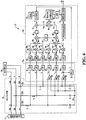
- FIG. 6 another motor drive power converter embodiment 10 is shown, including an LCL filter circuit 20, a rectifier 30, intermediate DC link circuit 40 and inverter 50 operated by a motor drive controller 60 generally as described above to power a motor or other AC load 6 using power from an AC input source 2.
- the LCL filter 20 in Fig. 6 includes series circuits individually including two series-connected inductors (La and Lu, etc.) with corresponding capacitor circuit branches 22 connecting the series circuits with three filter capacitors C a , C b and C c connected in a "Y" configuration with each filter capacitor C connected between a corresponding one of the capacitor circuit branches 22 and a common connection node 24 (e.g., a neutral node).
- the filter circuit 20 is an L-C configuration with only a single inductor in each of the series circuits, such as where the motor drive 10 is used in combination with an input transformer 3, in which case the inductors La, Lb and Lc can be omitted.
- the exemplary circuit 74a is constructed in generally the same manner as that shown in Fig. 2 above, with the differential amplifiers 80 measuring line-neutral voltages V an , V bn and V cn instead of line-to-line voltages as was the case in the delta-connected configuration of Figs. 1 and 2 .
- These voltages and the measured branch currents i a , i b and i c are low pass filtered via filter circuits 81 and converted to digital form via the analog-to-digital converters 82.
- the converters 82 operate concurrently to sample and convert the corresponding currents and voltages, with the converted voltages representing line-to-neutral voltages v an , v bn and v cn as shown in Fig. 6 . These voltages are squared via the multipliers 84 and the squared results are summed via the summation components 85 as in the above example of Fig. 2 . Unlike the case in Fig. 2 , however, the computed expected DC equivalent voltage value 75 is not delayed in the Y-connected case of Fig. 6 , and is instead provided directly to the summation component 90 for subtraction of the measured DC equivalent voltage value 77 to derive the voltage change value 79.
- the filter capacitor degradation detection system 70 in this case operates as described above in connection with Figs. 1 and 2 with the system 70 measuring filter circuit branch currents and voltages associated with the filter 20, computing expected DC equivalent voltage values using the measured currents and the impedance value Z, computing measured DC equivalent voltage values, and computing the DC equivalent voltage change values 79 representing deviations of the measured DC equivalent voltage value 77 and the expected DC equivalent voltage value 75 in each of a plurality of sample cycles, where the computed values and the resulting voltage change value 79 may be stored in the electronic memory 73 in certain embodiments.
- the system 70 selectively identifies one or more filter capacitor degradation conditions in the filter circuit 20 at least partially according to the voltage change values as discussed above, for example, through threshold comparison.
- the system may employ different threshold values 76 for delta and Y-connected filter circuit capacitor bank in the circuit 20, where the DC equivalent voltage change value thresholds 76 may be set according to a predetermined amount (e.g. 20% in one example) of tolerable variation in the capacitance value of the filter circuit capacitors C a , C b and C c .
- a predetermined amount e.g. 20% in one example
Landscapes
- Physics & Mathematics (AREA)
- General Physics & Mathematics (AREA)
- Engineering & Computer Science (AREA)
- Power Engineering (AREA)
- Inverter Devices (AREA)
- Measurement Of Current Or Voltage (AREA)
- Electric Propulsion And Braking For Vehicles (AREA)
- Testing Electric Properties And Detecting Electric Faults (AREA)
- Power Conversion In General (AREA)
Claims (15)
- Procédé (100) de détection d'une dégradation de condensateur dans un circuit de filtrage (20), le procédé (100) comprenant :la mesure (102) d'une pluralité de courants (ia, ib, ic) de branche de circuit de filtrage et d'une pluralité de tensions (Vab, Vbc, Vca) de circuit de filtrage associées au circuit de filtrage (20);le calcul (110) d'une valeur de tension équivalente CC attendue présente (75) au moins partiellement selon la pluralité de courants de branche de circuit de filtrage (ia, ib, ic) et d'une valeur d'impédance de condensateur de filtrage (Z) ;le stockage (112) de la valeur de tension équivalente CC attendue présente (75) dans une mémoire électronique (73) ;le calcul (114) d'une valeur de tension équivalente CC mesurée présente (77) au moins partiellement selon la pluralité de tensions de circuit de filtrage (Vab, Vbc, Vca) ;le stockage (116) de la valeur de tension équivalente CC mesurée présente (77) dans la mémoire électronique (73) ;le calcul (120) d'une valeur de changement de tension (79) représentant une dérive de tension d'une valeur de tension équivalente CC mesurée stockée (77) et d'une valeur de tension équivalente CC attendue stockée (75) dans la mémoire électronique (73); etl'identification sélective (124) d'une condition de dégradation de condensateur de filtrage dans le circuit de filtrage (20) au moins partiellement selon la valeur de changement de tension (79).
- Procédé (100) de la revendication 1, comprenant le calcul (108) de la valeur d'impédance de condensateur de filtrage (Z) au moins partiellement selon une fréquence d'entrée fondamentale (f) d'une tension ou d'un courant dans le circuit de filtrage (20).
- Procédé (100) de la revendication 2, comprenant :la mesure (106) de la fréquence d'entrée fondamentale (f) ; etle calcul (108) de la valeur d'impédance de condensateur de filtrage (Z) selon la fréquence d'entrée fondamentale mesurée (f) et une valeur de capacitance de filtre nominale (93).
- Procédé (100) selon l'une quelconque des revendications 1 à 3, dans lequel le calcul (110) de la valeur de tension équivalente CC attendue présente (75) comprend :le calcul d'une somme de valeur de carrés de courant de la pluralité de courants de branche de circuit de filtrage (Ia, Ib, Ic) ;la division de la somme de valeur de carrés de courant par un entier correspondant au nombre de courants de branche de filtrage dans le circuit de filtrage (20) ;le calcul d'une racine carrée de la somme divisée de valeur de carrés de courant ; etla multiplication de la racine carrée par la valeur d'impédance de condensateur de filtrage (Z).
- Procédé (100) de la revendication 4, dans lequel le calcul (114) de la valeur de tension équivalente CC mesurée présente (77) comprend :le calcul d'une somme de valeur de carrés de tension de la pluralité de tensions d'un circuit de filtrage (Vab, Vbc, Vca) ; etla division de la somme de valeur de carrés de tension par un entier correspondant au nombre de courants de branche de filtrage dans le circuit de filtrage (20).
- Procédé (100) selon l'une quelconque des revendications 1 à 5, dans lequel le calcul (120) de la valeur de changement de tension (79) comprend le calcul d'une dérive de tension de la valeur de tension équivalente CC mesurée présente (77) et d'une valeur de tension équivalente CC attendue retardée (75) calculée en utilisant des courants de branche de circuit de filtrage précédemment mesurés (Ia, Ib, Ic) ; et/ou
dans lequel un calcul (114) de la valeur de tension équivalente CC mesurée présente (77) comprend :le calcul d'une somme d'une valeur de carrés de tension de la pluralité de tensions d'un circuit de filtrage (Vab, Vbc, Vca) ; etla division de la somme de valeur de carrés de tension par un entier correspondant au nombre de courants de branche de filtrage dans le circuit de filtrage (20). - Procédé (100) de la revendication 6, comprenant le calcul (108) de la valeur d'impédance de condensateur de filtrage (Z) au moins partiellement selon une fréquence d'entrée fondamentale (f) d'une tension ou d'un courant dans le circuit de filtrage (20) ; et/ou
dans lequel l'identification sélective (124) d'une condition de dégradation de condensateur de filtre dans le circuit de filtrage (20) comprend :le calcul d'une valeur de changement de tension moyenne pondérée (95) selon une valeur de changement de tension présente (79) et une pluralité de valeurs de changement de tension précédentes (79) ;le calcul d'une valeur absolue (97) de la valeur de changement de tension moyenne pondérée ;la comparaison (122) de la valeur absolue (97) à une valeur de seuil (76) ; etl'identification (124) d'une condition de dégradation de condensateur de filtrage dans le circuit de filtrage (20) si la valeur absolue (97) est supérieure ou égale à la valeur de seuil (76). - Procédé (100) selon l'une quelconque des revendications 1 à 7, dans lequel le calcul (114) de la valeur de tension équivalente CC mesurée présente (77) comprend :le calcul d'une somme de valeur de carrés de tension de la pluralité de tensions de circuit de filtrage (Vab, Vbc, Vca) ; etla division de la somme de valeur de carrés de tension par un entier correspondant au nombre de courants de branche de filtrage dans le circuit de filtrage (20).
- Procédé (100) selon l'une quelconque des revendications 1 à 8, dans lequel l'identification sélective (124) d'une condition de dégradation de condensateur de filtrage dans le circuit de filtrage (20) comprend :le calcul d'une valeur de changement de tension moyenne pondérée (95) selon une valeur de changement de tension présente (79) et une pluralité de valeurs de changement de tension précédentes (79) ;le calcul d'une valeur absolue (97) de la valeur de changement de tension moyenne fluctuante ;la comparaison (122) de la valeur absolue (97) à une valeur de seuil (76) ; etl'identification (124) d'une condition de dégradation d'un condensateur de filtrage dans le circuit de filtrage (20) si la valeur absolue (97) est supérieure ou égale à la valeur de seuil (76) ; et/oudans lequel le calcul (120) de la valeur de changement de tension (79) comprend la soustraction de la valeur de tension équivalente CC mesurée stockée (77) à la valeur de tension équivalente CC attendue stockée (75).
- Procédé (100) selon l'une quelconque des revendications 1 à 9, dans lequel le calcul (120) de la valeur de changement de tension (79) comprend la soustraction de la valeur de tension équivalente CC mesurée stockée (77) à la valeur de tension équivalente CC attendue stockée (75) ; et/ou
dans lequel le calcul (120) de la valeur de changement de tension (79) comprend la soustraction de la valeur de tension équivalente CC mesurée présente (77) à une valeur de tension équivalente CC attendue retardée (75) calculée en utilisant des courants de branche de circuit de filtrage précédemment mesurés (Ia, Ib, Ic). - Support non transitoire lisible par un ordinateur (73) avec des instructions informatiques exécutables par un ordinateur pour effectuer le procédé selon l'une quelconque des revendications 1 à 10.
- Dispositif de conversion de puissance(10) comprenant :une entrée d'un convertisseur de puissance (4) fonctionnant pour recevoir une puissance d'entrée CA multiphase ;un redresseur frontal actif, ou redresseur AFE (Active Front End), (30) ;un circuit de filtrage (20) couplé entre l'entrée du convertisseur de puissance (4) et le redresseur AFE (30), le circuit de filtrage (20) comprenant les premier, deuxième et troisième circuits en série comprenant individuellement au moins un inducteur de filtrage (Lu, Lv, Lw) couplé entre une phase correspondante de l'entrée du convertisseur de puissance (4) et une phase correspondante de l'entrée CA triphasée du redresseur AFE (30), les première, deuxième et troisième branches du circuit de condensateur (22a, 22b, 22c) connectées respectivement au premier, deuxième et troisième circuits en série, et trois condensateurs de filtrage (Cab, Cbc, Cca) avec chaque condensateur de filtrage connecté à au moins une des branches de circuit de condensateur (22) ;un circuit de mesure (74a) couplé de manière opérationnelle au circuit de filtrage d'entrée (20) pour mesurer une pluralité de courants de branche de circuit de filtrage (Ia, Ib, Ic) associés au circuit de filtrage (20) et une pluralité de tensions de circuit de filtrage (Vab, Vbc, Vca) associés au circuit de filtrage (20) ; etau moins un processeur (71) programmé pour effectuer :le calcul (110) d'une valeur de tension équivalente CC attendue présente (75) au moins partiellement selon la pluralité de courants de branche de circuit de filtrage (ia, ib, ic) et d'une valeur d'impédance de condensateur de filtrage (Z) ;le calcul (114) d'une valeur de tension équivalente CC mesurée présente (77) au moins partiellement selon la pluralité de tensions de circuit de filtrage (Vab, Vbc, Vca) ;le calcul (120) d'une valeur de changement de tension (79) représentant une dérive de tension d'une valeur de tension équivalente CC mesurée stockée (77) et d'une valeur de tension équivalente CC attendue stockée (75) dans la mémoire électronique (73); etl'identification sélective (124) d'une condition de dégradation de condensateur de filtrage dans le circuit de filtrage (20) au moins partiellement selon la valeur de changement de tension (79).
- Système de conversion de puissance (10) de la revendication 12, comprenant une pluralité de circuits convertisseurs analogique-numérique (82) configurés pour simultanément échantillonner et convertir la pluralité de courants de branche de circuit de filtrage (Ia, Ib, Ic) et la pluralité de tensions de circuit de filtrage (Vab, Vbc, Vca) dans chacun d'une pluralité de cycles d'échantillonnage.
- Système de conversion de puissance (10) de la revendication 12 ou 13, dans lequel l'au moins un processeur (71) est programmé pour :calculer une valeur de changement de tension moyenne pondérée (95) selon une valeur de changement de tension présente (79) et une pluralité de valeurs de changement de tension précédentes (79) ;calculer une valeur absolue (97) de la valeur de changement de tension moyenne pondérée ;comparer (122) la valeur absolue (97) à une valeur de seuil (76) ; etidentifier (124) une condition de dégradation de condensateur de filtrage dans le circuit de filtrage (20) si la valeur absolue (97) est supérieure ou égale à la valeur de seuil (76) ; et/oudans lequel au moins un processeur (71) est programmé pour calculer (120) la valeur de changement de tension (79) en tant que dérive de tension de la valeur de tension équivalente CC mesurée présente (77) et une valeur de tension équivalente CC attendue retardée (75) calculée en utilisant des courants de branche de circuit de filtrage précédemment mesurés (Ia, Ib, Ic).
- Système de conversion de puissance (10) de la revendication 13 ou 14, dans lequel l'au moins un processeur (71) est programmé pour calculer (120) la valeur de changement de tension (79) en soustrayant la valeur de tension équivalente CC mesurée stockée (77) à la valeur de tension équivalente CC attendue stockée (75) ;
dans lequel l'au moins un processeur (71) est programmé pour calculer (120) la valeur de changement de tension (79) en soustrayant la valeur de tension équivalente CC mesurée présente (77) à une valeur de tension équivalente CC attendue retardée (75) calculée en utilisant des courants de branche de circuit de filtrage précédemment mesurés (Ia, Ib, Ic).
Applications Claiming Priority (1)
| Application Number | Priority Date | Filing Date | Title |
|---|---|---|---|
| US14/296,836 US9389263B2 (en) | 2014-06-05 | 2014-06-05 | Filter capacitor degradation identification using measured and expected voltage |
Publications (3)
| Publication Number | Publication Date |
|---|---|
| EP2953246A2 EP2953246A2 (fr) | 2015-12-09 |
| EP2953246A3 EP2953246A3 (fr) | 2016-05-18 |
| EP2953246B1 true EP2953246B1 (fr) | 2017-08-09 |
Family
ID=53276038
Family Applications (1)
| Application Number | Title | Priority Date | Filing Date |
|---|---|---|---|
| EP15170476.4A Active EP2953246B1 (fr) | 2014-06-05 | 2015-06-03 | Identification de la dégradation d'un condensateur de filtre au moyen d'une tension calculée et mesurée |
Country Status (2)
| Country | Link |
|---|---|
| US (1) | US9389263B2 (fr) |
| EP (1) | EP2953246B1 (fr) |
Families Citing this family (38)
| Publication number | Priority date | Publication date | Assignee | Title |
|---|---|---|---|---|
| CN104079182B (zh) * | 2014-06-18 | 2017-11-21 | 华为技术有限公司 | 逆变电源系统 |
| JP6247189B2 (ja) * | 2014-10-02 | 2017-12-13 | ファナック株式会社 | 直流リンク残留エネルギーの放電機能を有するモータ制御装置 |
| US10345348B2 (en) * | 2014-11-04 | 2019-07-09 | Stmicroelectronics S.R.L. | Detection circuit for an active discharge circuit of an X-capacitor, related active discharge circuit, integrated circuit and method |
| CN104377727B (zh) * | 2014-11-17 | 2016-09-21 | 中国矿业大学 | 一种并网逆变器多目标协同优化的不平衡控制方法 |
| DE102015109285A1 (de) * | 2015-04-09 | 2016-10-13 | Weidmüller Interface GmbH & Co. KG | Elektrische Baugruppe sowie Messschaltung und Messverfahren zur Überwachung eines Bauelements der elektrischen Baugruppe |
| KR20170014665A (ko) * | 2015-07-30 | 2017-02-08 | 엘에스산전 주식회사 | 배터리 충방전 제어 장치 |
| DK3360243T3 (en) * | 2015-10-05 | 2021-03-22 | Heliox B V | A bidirectional power converter |
| FR3047573B1 (fr) * | 2016-02-10 | 2018-03-02 | Continental Automotive France | Procede de commande en tension d'un equipement monte dans un vehicule automobile |
| US10985644B1 (en) | 2016-06-25 | 2021-04-20 | Active-Semi, Inc. | Optimized gate driver for low voltage power loss protection system |
| US9705402B1 (en) * | 2016-06-25 | 2017-07-11 | Active-Semi, Inc. | Power loss protection integrated circuit |
| US10090675B1 (en) | 2016-06-25 | 2018-10-02 | Active-Semi, Inc. | Fast settlement of supplement converter for power loss protection system |
| US10826480B1 (en) | 2016-07-01 | 2020-11-03 | Active-Semi, Inc. | Gate driver to decrease EMI with shorter dead-time |
| CN106526331B (zh) * | 2016-10-09 | 2019-05-21 | 安徽四新电子有限责任公司 | 一种电容器测量装置 |
| CN106771783B (zh) * | 2017-02-14 | 2023-08-18 | 英孚康(浙江)工业技术有限公司 | 直流母线电容组健康监测电路 |
| US10732714B2 (en) | 2017-05-08 | 2020-08-04 | Cirrus Logic, Inc. | Integrated haptic system |
| US10832537B2 (en) | 2018-04-04 | 2020-11-10 | Cirrus Logic, Inc. | Methods and apparatus for outputting a haptic signal to a haptic transducer |
| US10158299B1 (en) * | 2018-04-18 | 2018-12-18 | Rockwell Automation Technologies, Inc. | Common voltage reduction for active front end drives |
| CN109061314B (zh) * | 2018-06-29 | 2021-05-11 | 华为技术有限公司 | 一种检测逆变器的滤波电容容值的方法及装置 |
| GB201817495D0 (en) | 2018-10-26 | 2018-12-12 | Cirrus Logic Int Semiconductor Ltd | A force sensing system and method |
| US12035445B2 (en) | 2019-03-29 | 2024-07-09 | Cirrus Logic Inc. | Resonant tracking of an electromagnetic load |
| US11283337B2 (en) * | 2019-03-29 | 2022-03-22 | Cirrus Logic, Inc. | Methods and systems for improving transducer dynamics |
| US11307631B2 (en) * | 2019-05-29 | 2022-04-19 | Advanced Micro Devices, Inc. | Dynamic voltage frequency scaling based on active memory barriers |
| US11211879B2 (en) | 2019-09-23 | 2021-12-28 | Rockwell Automation Technologies, Inc. | Capacitor size reduction and lifetime extension for cascaded H-bridge drives |
| ES2943261T3 (es) * | 2019-11-12 | 2023-06-12 | Schneider Toshiba Inverter Europe Sas | Dispositivo electrónico y método para determinar al menos un parámetro característico de un conjunto de conexión conectado entre un convertidor y una máquina eléctrica, cadena de suministro de potencia relacionada y programa informático |
| US12276687B2 (en) | 2019-12-05 | 2025-04-15 | Cirrus Logic Inc. | Methods and systems for estimating coil impedance of an electromagnetic transducer |
| US11428750B1 (en) * | 2019-12-12 | 2022-08-30 | Smart Wires Inc. | Monitoring non-uniform capacitor and IGBT degradation with current sensors |
| US12244253B2 (en) | 2020-04-16 | 2025-03-04 | Cirrus Logic Inc. | Restricting undesired movement of a haptic actuator |
| US11496254B2 (en) * | 2020-08-28 | 2022-11-08 | Rockwell Automation Technologies, Inc. | System and method for testing filters in redundant signal paths |
| EP4193442A1 (fr) | 2020-09-14 | 2023-06-14 | Hitachi Energy Switzerland AG | Détection de panne dans des batteries de condensateurs de dérivation |
| US12255549B1 (en) * | 2020-10-21 | 2025-03-18 | Smart Wires Inc. | High current Voltage-Source Converter |
| CN114441875B (zh) * | 2020-11-02 | 2025-01-07 | 许继电气股份有限公司 | 变流器交流滤波电容失效检测方法、装置以及变流器系统 |
| EP4020782A1 (fr) * | 2020-12-23 | 2022-06-29 | ABB Schweiz AG | Détermination des paramètres d'un circuit de filtrage |
| CN113489358B (zh) * | 2021-06-29 | 2022-07-01 | 南京工程学院 | 一种逆变器的参数在线辨识方法 |
| US11923676B2 (en) * | 2021-08-12 | 2024-03-05 | Mho Technologies Corp. | Method for identifying element failure in capacitor banks |
| US12025680B2 (en) * | 2021-11-16 | 2024-07-02 | City University Of Hong Kong | Method and monitoring device using the same for estimating intrinsic parameters of encapsulated capacitor |
| EP4191265A1 (fr) * | 2021-12-01 | 2023-06-07 | dSPACE GmbH | Dispositif de test pour tester un appareil de commande électronique de puissance et module électronique de puissance pour un tel dispositif de test |
| US12370617B2 (en) * | 2022-01-25 | 2025-07-29 | Esab Ab | Controller method and apparatus for welding system |
| CN116047153B (zh) * | 2023-02-23 | 2025-10-10 | 中国电子产品可靠性与环境试验研究所((工业和信息化部电子第五研究所)(中国赛宝实验室)) | 系统故障感知方法、装置、计算机设备和存储介质 |
Family Cites Families (63)
| Publication number | Priority date | Publication date | Assignee | Title |
|---|---|---|---|---|
| DE3020110A1 (de) * | 1980-05-27 | 1982-01-14 | Siemens AG, 1000 Berlin und 8000 München | Ueberwachungseinrichtung fuer die kondensatorbatterien eines drehstrom- filterkreises |
| JPS61243375A (ja) * | 1985-04-19 | 1986-10-29 | Tokyo Electric Power Co Inc:The | 電力ケ−ブルの絶縁体劣化診断法 |
| US5319513A (en) | 1991-10-17 | 1994-06-07 | Trans-Coil, Inc. | Harmonic monitor and protection module |
| US5491725A (en) | 1993-09-07 | 1996-02-13 | Rockwell International Corporation | Tracking filter and quadrature-phase reference generator |
| JPH0919003A (ja) | 1995-06-27 | 1997-01-17 | Honda Motor Co Ltd | 電動車両におけるコンデンサの劣化判定装置 |
| US5796258A (en) | 1997-01-30 | 1998-08-18 | Abb Power T&D Company, Inc. | Adaptive quadrilateral characteristic distance relay |
| US6515462B2 (en) | 2000-02-10 | 2003-02-04 | Rohm Co., Ltd. | Power supply device |
| US6269010B1 (en) | 2000-02-29 | 2001-07-31 | Rockwell Technologies, Llc | CSI based drive having feedforward control of inverter input voltage |
| US6166929A (en) | 2000-02-29 | 2000-12-26 | Rockwell Technologies, Llc | CSI based drive having active damping control |
| US6366483B1 (en) | 2000-07-24 | 2002-04-02 | Rockwell Automation Technologies, Inc. | PWM rectifier having de-coupled power factor and output current control loops |
| US6667866B1 (en) | 2000-12-28 | 2003-12-23 | Abb Technology Ag | Virtual ground following single-phase trip |
| JP4013483B2 (ja) | 2001-02-13 | 2007-11-28 | 株式会社日立製作所 | 電力変換器の制御装置 |
| US6525951B1 (en) | 2002-01-25 | 2003-02-25 | Derek Albert Paice | Simplified wye connected 3-phase to 9-phase auto-transformer |
| JP2004317345A (ja) | 2003-04-17 | 2004-11-11 | Agilent Technol Inc | 狭帯域増幅器およびインピーダンス測定装置 |
| SE0303615D0 (sv) | 2003-12-31 | 2003-12-31 | Abb Ab | Method and device for Fault Detection in Transformers |
| US7782009B2 (en) | 2004-08-24 | 2010-08-24 | Rockwell Automation Technologies, Inc. | Adjustable speed drive protection |
| AU2005295599B2 (en) | 2004-10-18 | 2010-04-22 | Cooper Technologies Company | Corrective device protection |
| US7495938B2 (en) | 2005-04-15 | 2009-02-24 | Rockwell Automation Technologies, Inc. | DC voltage balance control for three-level NPC power converters with even-order harmonic elimination scheme |
| US7274576B1 (en) | 2006-03-01 | 2007-09-25 | Rockwell Automation Technologies, Inc. | Power converter with reduced common mode voltage |
| US7309973B2 (en) | 2006-04-24 | 2007-12-18 | Power Conservation Ltd | Mitigation of harmonic currents and conservation of power in non-linear load systems |
| EP2874297B1 (fr) | 2006-06-06 | 2023-09-27 | Ideal Power Inc. | Convertisseur de puissance abaisseur-élévateur |
| EP1870991B1 (fr) | 2006-06-23 | 2014-01-15 | ABB Schweiz AG | Méthode de commande d'un circuit onduleur |
| US7511976B2 (en) | 2006-06-27 | 2009-03-31 | Rockwell Automation Technologies, Inc. | Self powered supply for power converter switch driver |
| JP2010511876A (ja) | 2006-12-08 | 2010-04-15 | シーメンス アクチエンゲゼルシヤフト | キャパシタンス測定による変換器のコンデンサの経年劣化の監視 |
| US7495410B2 (en) | 2007-01-30 | 2009-02-24 | Rockwell Automation Technologies, Inc. | Systems and methods for improved motor drive power factor control |
| KR100998577B1 (ko) | 2007-08-29 | 2010-12-07 | 주식회사 와튼 | 전력변환장치의 노화상태 진단장치 및 이의 진단방법 |
| US7830269B2 (en) | 2007-09-14 | 2010-11-09 | Astec International Limited | Health monitoring for power converter capacitors |
| US7683568B2 (en) | 2007-09-28 | 2010-03-23 | Rockwell Automation Technologies, Inc. | Motor drive using flux adjustment to control power factor |
| US7800348B2 (en) | 2007-11-21 | 2010-09-21 | Rockwell Automation Technologies, Inc. | Motor drive with VAR compensation |
| US8862426B2 (en) * | 2007-12-20 | 2014-10-14 | International Business Machines Corporation | Method and test system for fast determination of parameter variation statistics |
| US8030791B2 (en) | 2008-07-31 | 2011-10-04 | Rockwell Automation Technologies, Inc. | Current source converter-based wind energy system |
| US8009450B2 (en) | 2008-08-26 | 2011-08-30 | Rockwell Automation Technologies, Inc. | Method and apparatus for phase current balance in active converter with unbalanced AC line voltage source |
| US7990097B2 (en) | 2008-09-29 | 2011-08-02 | Rockwell Automation Technologies, Inc. | Power conversion system and method for active damping of common mode resonance |
| US8044631B2 (en) | 2008-12-30 | 2011-10-25 | Rockwell Automation Technologies, Inc. | Power conversion systems and methods for controlling harmonic distortion |
| CN201393056Y (zh) | 2009-04-28 | 2010-01-27 | 山东山大奥太电气有限公司 | 一种逆变器的保护检测装置 |
| CA2763930C (fr) | 2009-06-18 | 2016-07-26 | Abb Technology Ag | Agencement d'echange de puissance |
| CN101995529B (zh) | 2009-08-21 | 2015-01-28 | 维斯塔斯风力系统集团公司 | 用于风力涡轮发电机中的电力滤波器的监视以及电力滤波器失效的检测的系统和方法 |
| US8587160B2 (en) | 2009-09-04 | 2013-11-19 | Rockwell Automation Technologies, Inc. | Grid fault ride-through for current source converter-based wind energy conversion systems |
| US8352203B2 (en) | 2009-11-30 | 2013-01-08 | Rockwell Automation Technologies, Inc. | Digital implementation of a tracking filter |
| US8259426B2 (en) | 2010-05-28 | 2012-09-04 | Rockwell Automation Technologies, Inc. | Variable frequency drive and methods for filter capacitor fault detection |
| US9054589B2 (en) | 2010-05-28 | 2015-06-09 | Rockwell Automation Technologies, Inc. | Method and apparatus for detecting power converter capacitor degradation using negative sequence currents |
| CN103026572B (zh) | 2010-07-23 | 2015-07-01 | Abb技术有限公司 | 用于电容器组保护的方法和装置 |
| ES2424041T3 (es) | 2010-09-30 | 2013-09-26 | Schneider Electric USA, Inc. | Sistemas, procedimientos y dispositivos para la monitorización de una batería de condensadores |
| US8698507B2 (en) * | 2010-12-21 | 2014-04-15 | Eneraiser Technology Co., Ltd. | DC capacitor degradation alarm circuit |
| SG191407A1 (en) | 2011-01-04 | 2013-08-30 | Zik Energy Points Inc | Method and system for energy efficiency and sustainability management |
| US8648610B2 (en) * | 2011-01-11 | 2014-02-11 | Denso Corporation | Signal input circuit and integrated circuit |
| US8643383B2 (en) | 2011-01-28 | 2014-02-04 | Rockwell Automation Technologies, Inc. | Drive failure protection |
| CN103328991B (zh) | 2011-02-16 | 2015-12-16 | Abb研究有限公司 | 用于y-y连接电容器组中内部故障检测的方法和装置 |
| ES2528443T3 (es) | 2011-02-16 | 2015-02-10 | Abb Research Ltd. | Método y disposición para detectar un fallo interno en un banco de condensadores conectado en puente en H |
| FR2980053B1 (fr) | 2011-09-13 | 2013-10-04 | Renault Sa | Procede de surveillance du filtre capacitif d'un chargeur de batterie. |
| KR101220230B1 (ko) | 2011-09-27 | 2013-01-09 | 카코뉴에너지 주식회사 | 계통 연계형 병렬 인버터를 이용한 태양광 발전 시스템 |
| US8816729B2 (en) | 2011-11-14 | 2014-08-26 | Rockwell Automation Technologies, Inc. | Phase-locked-loop with quadrature tracking filter for synchronizing an electric grid |
| US8704571B2 (en) | 2011-11-14 | 2014-04-22 | Rockwell Automation Technologies, Inc. | Phase-locked-loop with quadrature tracking filter for synchronizing an electric grid |
| US8729844B2 (en) | 2012-01-18 | 2014-05-20 | Hamilton Sundstrand Corporation | Power converter with asymmetric phase shift autotransformer for alternating current (AC) motor |
| JP5664589B2 (ja) | 2012-04-20 | 2015-02-04 | 株式会社安川電機 | 電源回生コンバータおよび電力変換装置 |
| US9653984B2 (en) | 2012-04-30 | 2017-05-16 | Rockwell Automation Technologies, Inc. | Filter capacitor degradation detection apparatus and method |
| ITMI20121191A1 (it) * | 2012-07-06 | 2014-01-07 | Gen Electric | Sistemi, procedimenti, e dispositivi per la stima della capacita' di condensatori di potenza |
| US9318944B2 (en) | 2013-04-29 | 2016-04-19 | Rockwell Automation Technologies, Inc. | Methods and apparatus for active front end filter capacitor degradation detection |
| CN104283441B (zh) | 2013-07-12 | 2017-08-11 | 尼得科控制技术有限公司 | 一种直流电源及提供直流电源的方法 |
| US9294005B2 (en) | 2013-10-01 | 2016-03-22 | Rockwell Automation Technologies, Inc. | Method and apparatus for detecting AFE filter capacitor degradation |
| US9651592B2 (en) | 2013-12-03 | 2017-05-16 | Rockwell Automation Technologies, Inc. | Impedance detector apparatus and method |
| US9488686B2 (en) | 2014-02-24 | 2016-11-08 | Rockwell Automation Technologies, Inc. | Filter capacitor degradation identification using computed current |
| US9490690B2 (en) | 2014-03-11 | 2016-11-08 | Rockwell Automation Technologies, Inc. | Filter capacitor degradation identification using computed power |
-
2014
- 2014-06-05 US US14/296,836 patent/US9389263B2/en active Active
-
2015
- 2015-06-03 EP EP15170476.4A patent/EP2953246B1/fr active Active
Non-Patent Citations (1)
| Title |
|---|
| None * |
Also Published As
| Publication number | Publication date |
|---|---|
| US9389263B2 (en) | 2016-07-12 |
| US20150355259A1 (en) | 2015-12-10 |
| EP2953246A3 (fr) | 2016-05-18 |
| EP2953246A2 (fr) | 2015-12-09 |
Similar Documents
| Publication | Publication Date | Title |
|---|---|---|
| US9389263B2 (en) | Filter capacitor degradation identification using measured and expected voltage | |
| US9488686B2 (en) | Filter capacitor degradation identification using computed current | |
| US9490690B2 (en) | Filter capacitor degradation identification using computed power | |
| EP2814150B1 (fr) | Procédés et appareil pour détecter la dégradation active d'un condensateur de filtre d'extrémité avant | |
| US9294005B2 (en) | Method and apparatus for detecting AFE filter capacitor degradation | |
| EP2660961B1 (fr) | Appareil de détection de résonance de convertisseur de puissance et procédé | |
| CN107064750A (zh) | 滤波电容器的退化及校正 | |
| WO2017083527A1 (fr) | Procédé de diagnostic en ligne pour des défaillances de commutation dans des convertisseurs de puissance | |
| CN108093672B (zh) | 逆变器基板、连接顺序的判断方法、缺相判断方法 | |
| KR101929519B1 (ko) | 불평형 커패시터 전압을 가지는 3 레벨 npc 인버터 시스템 및 그 제어 방법 | |
| US10014792B2 (en) | Multi-phase electric drive and power unit thereof for use with a multi-phase AC load | |
| JP2019158456A (ja) | 正弦波フィルタのコンデンサ容量判定装置 | |
| CN102710108B (zh) | 功率转换器和操作方法 | |
| EP3266111B1 (fr) | Procédé et appareil de résolution de réduction d'ondulation aflc de ligne de condensateur pfc sans filtres passifs | |
| JP2016015847A (ja) | マルチレベル電力変換器 | |
| JP6281117B2 (ja) | 電力変換装置 | |
| Hong et al. | An Online Degradation Detection Method for Grid-Connected Converters with LCL Filter | |
| Herman et al. | Comparison of circuit configuration and filtering performance between parallel and series hybrid active filter | |
| Misra | Decoupled Vector Control of Grid Side Converter with Less Number of Sensors under imbalanced Grid Conditions |
Legal Events
| Date | Code | Title | Description |
|---|---|---|---|
| PUAI | Public reference made under article 153(3) epc to a published international application that has entered the european phase |
Free format text: ORIGINAL CODE: 0009012 |
|
| AK | Designated contracting states |
Kind code of ref document: A2 Designated state(s): AL AT BE BG CH CY CZ DE DK EE ES FI FR GB GR HR HU IE IS IT LI LT LU LV MC MK MT NL NO PL PT RO RS SE SI SK SM TR |
|
| AX | Request for extension of the european patent |
Extension state: BA ME |
|
| PUAL | Search report despatched |
Free format text: ORIGINAL CODE: 0009013 |
|
| AK | Designated contracting states |
Kind code of ref document: A3 Designated state(s): AL AT BE BG CH CY CZ DE DK EE ES FI FR GB GR HR HU IE IS IT LI LT LU LV MC MK MT NL NO PL PT RO RS SE SI SK SM TR |
|
| AX | Request for extension of the european patent |
Extension state: BA ME |
|
| RIC1 | Information provided on ipc code assigned before grant |
Ipc: G01R 31/02 20060101ALI20160414BHEP Ipc: G01R 27/26 20060101ALI20160414BHEP Ipc: G01R 19/00 20060101ALI20160414BHEP Ipc: G01R 31/34 20060101ALI20160414BHEP Ipc: H02M 1/12 20060101AFI20160414BHEP Ipc: G01R 31/42 20060101ALI20160414BHEP |
|
| RIN1 | Information on inventor provided before grant (corrected) |
Inventor name: SARTLER, CHRISTIAN Inventor name: PATEL, YOGESH Inventor name: WEI, LIXIANG Inventor name: PHILLIPS, MARK |
|
| 17P | Request for examination filed |
Effective date: 20161118 |
|
| RBV | Designated contracting states (corrected) |
Designated state(s): AL AT BE BG CH CY CZ DE DK EE ES FI FR GB GR HR HU IE IS IT LI LT LU LV MC MK MT NL NO PL PT RO RS SE SI SK SM TR |
|
| GRAP | Despatch of communication of intention to grant a patent |
Free format text: ORIGINAL CODE: EPIDOSNIGR1 |
|
| INTG | Intention to grant announced |
Effective date: 20170331 |
|
| GRAS | Grant fee paid |
Free format text: ORIGINAL CODE: EPIDOSNIGR3 |
|
| GRAA | (expected) grant |
Free format text: ORIGINAL CODE: 0009210 |
|
| AK | Designated contracting states |
Kind code of ref document: B1 Designated state(s): AL AT BE BG CH CY CZ DE DK EE ES FI FR GB GR HR HU IE IS IT LI LT LU LV MC MK MT NL NO PL PT RO RS SE SI SK SM TR |
|
| REG | Reference to a national code |
Ref country code: GB Ref legal event code: FG4D |
|
| REG | Reference to a national code |
Ref country code: CH Ref legal event code: EP Ref country code: AT Ref legal event code: REF Ref document number: 917824 Country of ref document: AT Kind code of ref document: T Effective date: 20170815 |
|
| REG | Reference to a national code |
Ref country code: IE Ref legal event code: FG4D |
|
| REG | Reference to a national code |
Ref country code: DE Ref legal event code: R096 Ref document number: 602015003949 Country of ref document: DE |
|
| REG | Reference to a national code |
Ref country code: NL Ref legal event code: MP Effective date: 20170809 |
|
| REG | Reference to a national code |
Ref country code: LT Ref legal event code: MG4D |
|
| REG | Reference to a national code |
Ref country code: AT Ref legal event code: MK05 Ref document number: 917824 Country of ref document: AT Kind code of ref document: T Effective date: 20170809 |
|
| PG25 | Lapsed in a contracting state [announced via postgrant information from national office to epo] |
Ref country code: HR Free format text: LAPSE BECAUSE OF FAILURE TO SUBMIT A TRANSLATION OF THE DESCRIPTION OR TO PAY THE FEE WITHIN THE PRESCRIBED TIME-LIMIT Effective date: 20170809 Ref country code: LT Free format text: LAPSE BECAUSE OF FAILURE TO SUBMIT A TRANSLATION OF THE DESCRIPTION OR TO PAY THE FEE WITHIN THE PRESCRIBED TIME-LIMIT Effective date: 20170809 Ref country code: SE Free format text: LAPSE BECAUSE OF FAILURE TO SUBMIT A TRANSLATION OF THE DESCRIPTION OR TO PAY THE FEE WITHIN THE PRESCRIBED TIME-LIMIT Effective date: 20170809 Ref country code: FI Free format text: LAPSE BECAUSE OF FAILURE TO SUBMIT A TRANSLATION OF THE DESCRIPTION OR TO PAY THE FEE WITHIN THE PRESCRIBED TIME-LIMIT Effective date: 20170809 Ref country code: NO Free format text: LAPSE BECAUSE OF FAILURE TO SUBMIT A TRANSLATION OF THE DESCRIPTION OR TO PAY THE FEE WITHIN THE PRESCRIBED TIME-LIMIT Effective date: 20171109 Ref country code: AT Free format text: LAPSE BECAUSE OF FAILURE TO SUBMIT A TRANSLATION OF THE DESCRIPTION OR TO PAY THE FEE WITHIN THE PRESCRIBED TIME-LIMIT Effective date: 20170809 Ref country code: NL Free format text: LAPSE BECAUSE OF FAILURE TO SUBMIT A TRANSLATION OF THE DESCRIPTION OR TO PAY THE FEE WITHIN THE PRESCRIBED TIME-LIMIT Effective date: 20170809 |
|
| PG25 | Lapsed in a contracting state [announced via postgrant information from national office to epo] |
Ref country code: IS Free format text: LAPSE BECAUSE OF FAILURE TO SUBMIT A TRANSLATION OF THE DESCRIPTION OR TO PAY THE FEE WITHIN THE PRESCRIBED TIME-LIMIT Effective date: 20171209 Ref country code: BG Free format text: LAPSE BECAUSE OF FAILURE TO SUBMIT A TRANSLATION OF THE DESCRIPTION OR TO PAY THE FEE WITHIN THE PRESCRIBED TIME-LIMIT Effective date: 20171109 Ref country code: PL Free format text: LAPSE BECAUSE OF FAILURE TO SUBMIT A TRANSLATION OF THE DESCRIPTION OR TO PAY THE FEE WITHIN THE PRESCRIBED TIME-LIMIT Effective date: 20170809 Ref country code: RS Free format text: LAPSE BECAUSE OF FAILURE TO SUBMIT A TRANSLATION OF THE DESCRIPTION OR TO PAY THE FEE WITHIN THE PRESCRIBED TIME-LIMIT Effective date: 20170809 Ref country code: LV Free format text: LAPSE BECAUSE OF FAILURE TO SUBMIT A TRANSLATION OF THE DESCRIPTION OR TO PAY THE FEE WITHIN THE PRESCRIBED TIME-LIMIT Effective date: 20170809 Ref country code: GR Free format text: LAPSE BECAUSE OF FAILURE TO SUBMIT A TRANSLATION OF THE DESCRIPTION OR TO PAY THE FEE WITHIN THE PRESCRIBED TIME-LIMIT Effective date: 20171110 Ref country code: ES Free format text: LAPSE BECAUSE OF FAILURE TO SUBMIT A TRANSLATION OF THE DESCRIPTION OR TO PAY THE FEE WITHIN THE PRESCRIBED TIME-LIMIT Effective date: 20170809 |
|
| PG25 | Lapsed in a contracting state [announced via postgrant information from national office to epo] |
Ref country code: CZ Free format text: LAPSE BECAUSE OF FAILURE TO SUBMIT A TRANSLATION OF THE DESCRIPTION OR TO PAY THE FEE WITHIN THE PRESCRIBED TIME-LIMIT Effective date: 20170809 Ref country code: DK Free format text: LAPSE BECAUSE OF FAILURE TO SUBMIT A TRANSLATION OF THE DESCRIPTION OR TO PAY THE FEE WITHIN THE PRESCRIBED TIME-LIMIT Effective date: 20170809 Ref country code: RO Free format text: LAPSE BECAUSE OF FAILURE TO SUBMIT A TRANSLATION OF THE DESCRIPTION OR TO PAY THE FEE WITHIN THE PRESCRIBED TIME-LIMIT Effective date: 20170809 |
|
| REG | Reference to a national code |
Ref country code: DE Ref legal event code: R097 Ref document number: 602015003949 Country of ref document: DE |
|
| PG25 | Lapsed in a contracting state [announced via postgrant information from national office to epo] |
Ref country code: SM Free format text: LAPSE BECAUSE OF FAILURE TO SUBMIT A TRANSLATION OF THE DESCRIPTION OR TO PAY THE FEE WITHIN THE PRESCRIBED TIME-LIMIT Effective date: 20170809 Ref country code: SK Free format text: LAPSE BECAUSE OF FAILURE TO SUBMIT A TRANSLATION OF THE DESCRIPTION OR TO PAY THE FEE WITHIN THE PRESCRIBED TIME-LIMIT Effective date: 20170809 Ref country code: EE Free format text: LAPSE BECAUSE OF FAILURE TO SUBMIT A TRANSLATION OF THE DESCRIPTION OR TO PAY THE FEE WITHIN THE PRESCRIBED TIME-LIMIT Effective date: 20170809 Ref country code: IT Free format text: LAPSE BECAUSE OF FAILURE TO SUBMIT A TRANSLATION OF THE DESCRIPTION OR TO PAY THE FEE WITHIN THE PRESCRIBED TIME-LIMIT Effective date: 20170809 |
|
| PLBE | No opposition filed within time limit |
Free format text: ORIGINAL CODE: 0009261 |
|
| STAA | Information on the status of an ep patent application or granted ep patent |
Free format text: STATUS: NO OPPOSITION FILED WITHIN TIME LIMIT |
|
| REG | Reference to a national code |
Ref country code: FR Ref legal event code: PLFP Year of fee payment: 4 |
|
| 26N | No opposition filed |
Effective date: 20180511 |
|
| PG25 | Lapsed in a contracting state [announced via postgrant information from national office to epo] |
Ref country code: SI Free format text: LAPSE BECAUSE OF FAILURE TO SUBMIT A TRANSLATION OF THE DESCRIPTION OR TO PAY THE FEE WITHIN THE PRESCRIBED TIME-LIMIT Effective date: 20170809 |
|
| REG | Reference to a national code |
Ref country code: CH Ref legal event code: PL |
|
| REG | Reference to a national code |
Ref country code: BE Ref legal event code: MM Effective date: 20180630 |
|
| REG | Reference to a national code |
Ref country code: IE Ref legal event code: MM4A |
|
| PG25 | Lapsed in a contracting state [announced via postgrant information from national office to epo] |
Ref country code: MC Free format text: LAPSE BECAUSE OF FAILURE TO SUBMIT A TRANSLATION OF THE DESCRIPTION OR TO PAY THE FEE WITHIN THE PRESCRIBED TIME-LIMIT Effective date: 20170809 Ref country code: LU Free format text: LAPSE BECAUSE OF NON-PAYMENT OF DUE FEES Effective date: 20180603 |
|
| PG25 | Lapsed in a contracting state [announced via postgrant information from national office to epo] |
Ref country code: CH Free format text: LAPSE BECAUSE OF NON-PAYMENT OF DUE FEES Effective date: 20180630 Ref country code: IE Free format text: LAPSE BECAUSE OF NON-PAYMENT OF DUE FEES Effective date: 20180603 Ref country code: LI Free format text: LAPSE BECAUSE OF NON-PAYMENT OF DUE FEES Effective date: 20180630 |
|
| PG25 | Lapsed in a contracting state [announced via postgrant information from national office to epo] |
Ref country code: BE Free format text: LAPSE BECAUSE OF NON-PAYMENT OF DUE FEES Effective date: 20180630 |
|
| PG25 | Lapsed in a contracting state [announced via postgrant information from national office to epo] |
Ref country code: MT Free format text: LAPSE BECAUSE OF NON-PAYMENT OF DUE FEES Effective date: 20180603 |
|
| PG25 | Lapsed in a contracting state [announced via postgrant information from national office to epo] |
Ref country code: TR Free format text: LAPSE BECAUSE OF FAILURE TO SUBMIT A TRANSLATION OF THE DESCRIPTION OR TO PAY THE FEE WITHIN THE PRESCRIBED TIME-LIMIT Effective date: 20170809 |
|
| PG25 | Lapsed in a contracting state [announced via postgrant information from national office to epo] |
Ref country code: PT Free format text: LAPSE BECAUSE OF FAILURE TO SUBMIT A TRANSLATION OF THE DESCRIPTION OR TO PAY THE FEE WITHIN THE PRESCRIBED TIME-LIMIT Effective date: 20170809 |
|
| PG25 | Lapsed in a contracting state [announced via postgrant information from national office to epo] |
Ref country code: CY Free format text: LAPSE BECAUSE OF FAILURE TO SUBMIT A TRANSLATION OF THE DESCRIPTION OR TO PAY THE FEE WITHIN THE PRESCRIBED TIME-LIMIT Effective date: 20170809 Ref country code: HU Free format text: LAPSE BECAUSE OF FAILURE TO SUBMIT A TRANSLATION OF THE DESCRIPTION OR TO PAY THE FEE WITHIN THE PRESCRIBED TIME-LIMIT; INVALID AB INITIO Effective date: 20150603 Ref country code: MK Free format text: LAPSE BECAUSE OF NON-PAYMENT OF DUE FEES Effective date: 20170809 |
|
| PG25 | Lapsed in a contracting state [announced via postgrant information from national office to epo] |
Ref country code: AL Free format text: LAPSE BECAUSE OF FAILURE TO SUBMIT A TRANSLATION OF THE DESCRIPTION OR TO PAY THE FEE WITHIN THE PRESCRIBED TIME-LIMIT Effective date: 20170809 |
|
| P01 | Opt-out of the competence of the unified patent court (upc) registered |
Effective date: 20230404 |
|
| PGFP | Annual fee paid to national office [announced via postgrant information from national office to epo] |
Ref country code: GB Payment date: 20260520 Year of fee payment: 12 |
|
| PGFP | Annual fee paid to national office [announced via postgrant information from national office to epo] |
Ref country code: DE Payment date: 20260520 Year of fee payment: 12 |
|
| PGFP | Annual fee paid to national office [announced via postgrant information from national office to epo] |
Ref country code: FR Payment date: 20260520 Year of fee payment: 12 |