EP2953253A1 - Dispositif de commande d'onduleur et dispositif périphérique associé - Google Patents
Dispositif de commande d'onduleur et dispositif périphérique associé Download PDFInfo
- Publication number
- EP2953253A1 EP2953253A1 EP13874145.9A EP13874145A EP2953253A1 EP 2953253 A1 EP2953253 A1 EP 2953253A1 EP 13874145 A EP13874145 A EP 13874145A EP 2953253 A1 EP2953253 A1 EP 2953253A1
- Authority
- EP
- European Patent Office
- Prior art keywords
- computation
- processing
- inverter
- cycle
- drive control
- Prior art date
- Legal status (The legal status is an assumption and is not a legal conclusion. Google has not performed a legal analysis and makes no representation as to the accuracy of the status listed.)
- Ceased
Links
Images

Classifications
-
- H—ELECTRICITY
- H02—GENERATION; CONVERSION OR DISTRIBUTION OF ELECTRIC POWER
- H02M—APPARATUS FOR CONVERSION BETWEEN AC AND AC, BETWEEN AC AND DC, OR BETWEEN DC AND DC, AND FOR USE WITH MAINS OR SIMILAR POWER SUPPLY SYSTEMS; CONVERSION OF DC OR AC INPUT POWER INTO SURGE OUTPUT POWER; CONTROL OR REGULATION THEREOF
- H02M7/00—Conversion of AC power input into DC power output; Conversion of DC power input into AC power output
- H02M7/42—Conversion of DC power input into AC power output without possibility of reversal
- H02M7/44—Conversion of DC power input into AC power output without possibility of reversal by static converters
- H02M7/48—Conversion of DC power input into AC power output without possibility of reversal by static converters using discharge tubes with control electrode or semiconductor devices with control electrode
-
- H—ELECTRICITY
- H02—GENERATION; CONVERSION OR DISTRIBUTION OF ELECTRIC POWER
- H02M—APPARATUS FOR CONVERSION BETWEEN AC AND AC, BETWEEN AC AND DC, OR BETWEEN DC AND DC, AND FOR USE WITH MAINS OR SIMILAR POWER SUPPLY SYSTEMS; CONVERSION OF DC OR AC INPUT POWER INTO SURGE OUTPUT POWER; CONTROL OR REGULATION THEREOF
- H02M1/00—Details of apparatus for conversion
- H02M1/0003—Details of control, feedback or regulation circuits
- H02M1/0012—Control circuits using digital or numerical techniques
Definitions
- the present invention relates to an inverter control device that operates an inverter according to an input signal from the outside and outputs an operation state thereof to the outside as an output signal.
- a programmable logic controller is frequently arranged as a host device of the inverter control device in a case where an inverter control device that performs variable speed operations and the like of a motor is used incorporated into a mechanical device or the like.
- the PLC provides operation commands to the inverter control device while monitoring an operation state of the inverter in order to realize necessary operations.
- PTL 1 proposes an inverter device in which such a PLC function is built-in.
- an inverter operation portion and a PLC portion in the inverter control device are independent. Accordingly, in order for the results calculated in the PLC portion to be applied to the operation portion of the inverter, a mechanism is necessary for the processing of the PLC portion and the processing of the operation portion of the inverter to be synchronized. Therefore, there are problems of the processing of the inverter device becoming complicated, and a high-end CPU being necessary in the inverter control device.
- the invention is made in view of the above circumstance, and an object thereof is to provide an inverter control device capable of high-speed application of the results of computation for a PLC portion to the operation control of an inverter without use of a high-end CPU.
- the invention provides an inverter control device including: drive control means for repeatedly performing operation control of an inverter based on input data and an operation state of the inverter in synchronization with a control cycle; external input means for making an externally input signal into input data of the drive control means; external output means for externally outputting output data of the drive control means; parameter means for storing data used by the drive control means for operation control of the inverter; communication means for performing communication for externally inputting and outputting commands for inverter control and a state quantity of the inverter; and computation means for carrying out computation process using externally input data via the external input means, data output from the drive control means, data stored in the parameter means or data output by the communication means, and supplying processing results thereof to the drive control means, wherein processing means for carrying out the drive control means carries out processing of the computation means in synchronization with the processing cycle set to an integer multiple of the control cycle of the drive control means.
- the processing means for carrying out the drive control means carries out processing of the computation means in synchronization with the processing cycle set to an integer multiple of the control cycle of the drive control means, and the processing results of the computation means are supplied to the drive control means, high speed application of the results of the processing of the computation means to be reflected in the processing of the drive control means (that is, the operation control of the inverter) is possible. Since the processing means for carrying out the drive control means carries out processing of the computation means in synchronization with the processing cycle set to an integer multiple of the control cycle of the drive control means, a special mechanism by which the processing of the drive control means and the processing of the computation means are synchronized is unnecessary.
- the processing means has a function of calculating a necessary time for processing of the computation means from a type and number of computation process carried out by the computation means, processing time for each type of computation process stored in advance and an integer multiple that is a comparison of the processing cycle and the control cycle, and outputting a warning in a case where the necessary time exceeds the time set in advance.
- a warning is output in a case where the processing time of the processing carried out by the computation means exceeds the time set in advance, it is possible to provide a user with the chance to review a content and processing cycle of the processing carried out by the computation means.
- a peripheral device of the inverter control device includes a function of calculating a necessary time for processing of the computation means from a type and number of computation processes carried out by the computation means, a processing time for each type of computation process stored in advance, and an integer multiple that is a ratio of the processing cycle and the control cycle, and outputting a warning in a case where the necessary time exceeds the time set in advance.
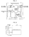
- Fig. 1 is a block diagram showing the configuration of an inverter control device 9 that is an embodiment of the invention.
- the inverter control device 9 includes drive control means 1, external input means 2, external output means 3, parameter means 4, communication means 5, and computation means 6.
- Each of these means is a program carried out by a processor provided in the inverter control device 9. That is, the inverter control device 9 according to the embodiment carries out processing of each means shown in Fig. 1 using shared calculation resources.
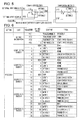
- a touch panel 10 and a PC loader 11 are used as peripheral devices along with the inverter control device 9, as shown in Fig. 2 .
- the peripheral devices are used as means for setting parameters for the inverter control device 9. The parameter settings of the inverter control device using the peripheral device will be described later.
- the drive control means 1 is means for performing operation of the inverter on the basis of an input signal and an operation state of the inverter.
- operation commands such as torque command values that indicate the torque to be generated by the motor that is a load on the inverter and speed command values that indicate a rotation speed are included in the input signal.
- the inverter operation specifically indicates pulse width moduration (PWM) control of a gate signal applied to a switching element connected to a motor in the inverter.
- PWM pulse width moduration
- the processor provided in the inverter control device 9 carries out processing as the drive control means 1 in synchronization with the predetermined control cycle.
- the external input means 2 is means for making an externally provided digital signal or analog signal an input signal to the drive control means 1.
- the external output means 3 is means for outputting a digital signal or an analog signal output by the drive control means 1 to the outside.
- the parameter means 4 is means that stores parameters referenced by the drive control means 1 in order to control the operation of the inverter.
- the parameter means 4 includes a nonvolatile memory able to be electrically re-written, such as an EEPROM, and a volatile memory, such as a RAM.
- the communication means 5 is means for performing communication for input and output with the outside of operation commands to be input to the drive control means 1, an operation state of the inverter obtained from the drive control means 1, and a state quantity such as an output frequency or a current.
- the computation means 6 executes a numerical value computation process such as edge detection processing that performs detection of a rising edge or falling edge, signal delay processing, logical computation processing, comparison processing or basic arithmetic operations with respect to signal data input to the external input means 2, signal data output from the drive control means 1, signal data stored in the parameter means 4, or signal data output by the communication means 5, and allows processing results thereof to be supplied as input signals to the drive control means 1 or the external output means 3, or stored in the parameter means 4.
- a numerical value computation process such as edge detection processing that performs detection of a rising edge or falling edge, signal delay processing, logical computation processing, comparison processing or basic arithmetic operations with respect to signal data input to the external input means 2, signal data output from the drive control means 1, signal data stored in the parameter means 4, or signal data output by the communication means 5, and allows processing results thereof to be supplied as input signals to the drive control means 1 or the external output means 3, or stored in the parameter means 4.
- the drive control means 1 includes processing means that performs time management of the computation means 6, external input means 2, external output means 3, and communication means 5, and controls each of these means.
- the processing means of the drive control means 1 makes the computation means 6 carry out processing in synchronization with the processing cycle set as an integer multiple of a control cycle of the drive control means 1.
- Figs. 3 to 5 are diagrams showing a configuration of Processes 1 to 3 that are examples of the processing carried out by the computation means 6 in the embodiment.
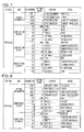
- Figs. 6 to 8 are drawings showing an example of processing configuration information in which the configuration of Processes 1 to 3 are defined.
- the processing configuration information of Processes 1 to 3 is stored in advance in a memory, not shown.
- the processing means of the drive control means 1 performs control for making the computation means 6 execute each of Processes 1 to 3 at a processing cycle set for each processing by referencing the processing configuration information.
- each piece of processing configuration information that defines Processes 1 to 3 is formed from one or a plurality of computation blocks.
- each computation block defines the content of the computation process carried out by the computation means 6, specifically the type of computation process, the input origin of the input data of the computation process, and the setting value of the computation process.
- One processing is configured by one or a plurality of computation processes.
- the processing configuration information in which one processing is defined includes a computation block for each computation process that configures the processing.
- One computation block includes five parameters.
- a first parameter defines the type of computation process, a second parameter Input 1, a third parameter Input 2, a fourth parameter Setting 1, and a fifth parameter Setting 2.
- Inputs 1 and 2 indicate first and second input data used in the computation process.
- Settings 1 and 2 change in definition according to the type of computation process. In a case of a READ or WRITE calculation, the combination of Settings 1 and 2 designates the read destination or write destination of the data. In a case where the calculation is addition, Setting 1 is an upper limiter of the addition results, and Setting 2 is a lower limiter of the addition results.
- Setting information is formed from the four parameters of setting number, the processing cycle, starting block and finishing block.
- the setting number in each processing configuration information item is the number of the processing defined by the processing configuration information.
- the processing cycle is a parameter that indicates how many times the control cycle the processing cycle of the processing defined by the processing configuration information is. In the embodiment, the processing cycle is set to an integer multiple of the control cycle. Therefore, the parameter of the processing cycle is an integer multiple value. However, in a case where 0 is set as the processing cycle, the 0 designates that the processing defined by the processing configuration information is not executed.
- the starting block is the number of the initial computation block in the processing defined by the processing configuration information.
- the finishing block is the number of the final computation block in the processing defined by the processing configuration information.
- the processing means of the drive control means 1 determines if the computation process of any computation blocks of any processing is carried out in any of the control cycles by referencing the processing configuration information for the above Processes 1 to 3, and Processes 1 to 3 are carried out by the computation means 6 in synchronization with the processing cycle set to an integer multiple of the control cycle.
- the type is 6000 that indicates READ
- Input 1 is 0 that indicates no input
- Input 2 is 0 that indicates no input
- Setting 1 is 10 that indicates Communication data 10 of the communication means 5
- Setting 2 is 1 that indicates a first data thereof. Therefore, the computation means 6 reads out Communication data 10-1 from the communication means 5 in carrying out of Computation block 1, as shown in Fig. 3 .
- the type is 6000 that indicates READ
- Input 1 is 0 that indicates no input
- Input 2 is 0 that indicates no input
- Setting 1 is 2 that indicates Parameter 2 of the parameter means 4
- Setting 2 is 3 that indicates a third parameter thereof. Therefore, the computation means 6 reads out Parameter 2-3 from the parameter means 4 in carrying out of Computation block 2, as shown in Fig. 3 .
- Computation block 3 in the processing configuration information of Process 1 in Fig. 6 the type is 1000 that indicates addition, Input 1 is 1 that indicates Computation block 1, Input 2 is 2 that indicates Computation block 2, Setting 1 is 100 that indicates the value of an upper limiter, and Setting 2 is 0 that indicates the value of a lower limiter. Therefore, the computation means 6 sets the upper limiter to 100 and the lower limiter to 0 in carrying out of Computation block 3 as shown in Fig. 3 , and performs addition of the output data of Computation block 1 and the output data of Computation block 2.
- Computation block 4 in the processing configuration information of Process 1 in Fig. 6 the type is 7000 that indicates WRITE, Input 1 is 3 that indicates Computation block 3, Input 2 is 101 that indicates Signal 1 of the external input means 2.
- Settings 1 and 2 are 4 and 1 that indicate Parameter 4-1 stored in a nonvolatile memory of the parameter means 4. Therefore, in carrying out of Computation block 4, as shown in Fig. 3 , the computation means 6 stores the output data of Computation block 3 as Parameter 4-1 in the nonvolatile memory of the parameter means 4 at the rising timing of Signal 1 of the external input means 2.
- Computation block 5 in the processing configuration information of Process 1 in Fig. 6 the type is 8000 that indicates MPX, Input 1 is 3 that indicates Computation block 3, Input 2 is 102 that indicates Signal 2 of the external input means 2, and Settings 1 and 2 are 2 and 3 that indicate Parameter 2-3. Therefore, the computation means 6 outputs Parameter 2-3 stored in the parameter means 4 in a case where Signal 2 of the external input means 2 is 0, and the output data of Computation block 3 in a case where other than 0 in carrying out of Computation block 5 as shown in Fig. 3 .
- the type is 6000 that indicates READ
- Input 1 is 0 that indicates no input
- Input 2 is 0 that indicates no input
- Setting 1 is 2 that indicates Parameter 5 held by the parameter means
- Setting 2 is 1 that indicates the first parameter thereof. Therefore, the computation means 6 reads out Parameter 5-1 from the parameter means 4 in carrying out of Computation block 6, as shown in Fig. 4 .
- Computation block 7 in the processing configuration information of Process 2 in Fig. 7 the type is 1000 that indicates addition, Input 1 is 6 that indicates Computation block 6, Input 2 is 8 that indicates Computation block 8, Setting 1 is 100 that indicates the value of the upper limiter, and Setting 2 is 0 that indicates the value of the lower limiter. Therefore, the computation means 6 sets the upper limiter to 100 and the lower limiter to 0 in carrying out of Computation block 7 as shown in Fig. 4 , and performs addition of the output data of Computation block 6 and the output data of Computation block 8.
- Computation block 8 in the processing configuration information of Process 2 in Fig. 7 the type is 4001 that indicates switching, Input 1 is 7 that indicates Computation block 7, Input 2 is 103 that indicates External input 3, Setting 1 is 0 that indicates the setting value 0, and Setting 2 is 0 that designates no function. Therefore, the computation means 6 outputs Computation block 7 when External input 3 is 0 and outputs the setting value 0 when External input 3 is not 0, in carrying out of Computation block 8, as shown in Fig. 4 .
- the type is 4100 that indicates holding of the value
- Input 1 is 201 that indicates Analog 1 of the external input
- Input 2 is 104 that indicates External input 4
- Setting 1 is 200 that indicates the value of the upper limiter
- Setting 2 is 0 that indicates the value of the lower limiter. Therefore, the computation means 6 outputs the value of Analog 1 of the external input when External input 4 is 0 and holds and outputs the previously output value when External input 4 is not 0, in carrying out of Computation block 9, as shown in Fig. 5 .
- Computation block 10 in the processing configuration information of Process 3 in Fig. 8 the type is 1000 that indicates addition, Input 1 is 9 that indicates Computation block 9, Input 2 is 8 that indicates Computation block 8, Setting 1 is 200 that indicates the value of the upper limiter, and Setting 2 is 0 that indicates the value of the lower limiter. Therefore, the computation means 6 sets the upper limiter to 200 and the lower limiter to 0 in carrying out of Computation block 10 as shown in Fig. 5 , and performs addition of the output data of Computation block 9 and the output data of Computation block 8.
- the output data of Computation block 5 and the output data of Computation block 10 are transferred to another computation block, not shown.
- the computation block which receives the output data of Computation block 5 may store the output data of Computation block 5 in the parameter means 4 as Parameter 2-3, or may carry out further calculation such as addition on the output data of Computation block 5.
- Communication data 10-1 of the communication means 5 is added with respect to Parameter 2-3 for each time the processing cycle is repeated. Accordingly, application of external communication data to the inverter control is possible without using the external input means 2 or the external output means 3.
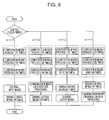
- Fig. 9 is a flowchart showing a processing flow of processing means of the drive control means 1.
- the inverter control device 9 carries out the respective processes of the external input means 2, external output means 3, parameter means 4, communication means 5, and computation means 6 in synchronization with a cycle corresponding to the control cycle for carrying out the drive control means 1, specifically a cycle with an integer multiple of the control cycle.
- the drive control means 1 that performs operation control of the inverter is necessary for processing at high speeds, and is necessarily operated in each control cycle.
- the external input means 2, external output means 3, parameter means 4, and communication means 5 may be carried out at each cycle thinned from the cycle in which the drive control means 1 is carried out in order to process at low speeds.
- the computation means 6 performs computation at the cycle in which the drive control means 1 is originally carried out, it is necessary to make the computation means 6 perform at a cycle within the constraints on the computation capacity of the inverter control device 9.
- the processing means of the drive control means 1 counts the number of times the control cycle is switched, and obtains the number of times n of the control cycle on the basis of the count value thereof.
- n is obtained by obtaining the least common multiple m of each integer that shows how many times the control cycle the processing cycle of each processing carried out by the computation means 6 is, and adding 1 to the remainder when the count value of the control cycle is divided by m.
- m is 4 that the least common multiple of 1, 2, and 4.
- n a value of 1 to 4.
- the processing means of the drive control means 1 determines the computation block carried out by the computation means 6 based on n in each control cycle.
- the processing means of the drive control means 1 calculates the number of computation blocks (number of ends rounded up) per control cycle for each Process 1 to 3 according to formula 1.
- number of computation blocks (finishing block - starting block + 1) / processing cycle formula 1
- the processing means of the drive control means 1 determines the computation block carried out by the computation means 6 in each control cycle based on the number of each processing block calculated for Processes 1 to 3.
- the processing of 2 blocks from Computation block 8 is carried out, since Computation block 8 is the finishing block, only the processing of Computation block 8 is carried out by the computation means 6.
- the processing means for carrying out the drive control means 1 makes the computation means 6 perform processing 1 to 3 at each processing cycle designated as an integer multiple of the control cycle according to the setting information as described above.
- the parameters thereof are externally read out from the parameter means 4 via the external output means 3, and processed externally according to the commands.
- the post-processing parameters are stored in the parameter means 4 via the external input means 2. In this case, a delay arises due to using the external output means 3 and the external input means 2, and high-speed inverter control is difficult.
- the computation means 6 carries out processing in which the parameter is read out from the parameter means 4, subjected to some processing, and reflected in the inverter control, without using the external output means 3 and the external input means 2. Accordingly, according to the embodiment, high speed inverter control is possible compared to the related art.
- the computation block that stores Parameter 4-1 as Parameter 2-3 when Signal 1 of the external input means 2 falls from 1 to 0 is provided, along with being configured so that Signal 1 of the external input means 2 falls from 1 to 0 in a case where the power source is recovered.
- Parameter 2-3 saved as Parameter 4-1 during the power outage is recovered as Parameter 2-3 when the power source recovers.
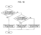
- the processing means for carrying out the drive control means 1, as shown in Fig. 9 allows Process 1 for which high speed is demanded to be carried out in synchronization with the same processing cycle as the control cycle, and allows Processes 2 and 3 for which high speed is not demanded to be carried out in synchronization with a processing cycle which is an integer multiple of 2 or more times the control cycle.
- the reason therefor is as follows.
- the processing cycle for performing the processing since it is necessary for the physical quantities such as the voltage, current and frequency of the inverter to be processed at high speeds, it is necessary for the processing cycle for performing the processing to be shortened. However, since high-speed processing is unnecessary for the man-machine interface, the processing cycle for performing the processing may be lengthened. Since the processing means for carrying out the drive control means 1 in the embodiment is synchronized to the processing cycle set to an integer multiple of the control cycle according to the setting information, as shown in Fig. 9 , and each processing is carried out by the computation means 6, it is possible for the processing cycle to be optimized according to the high speed demanded in the processing.
- the sum of the processing time of the computation blocks of Processes 1, 2, and 3 carried out in the n-th control cycle is obtained in formula 2.
- a plurality of types of computation blocks are carried out.
- the processing means of the drive control means 1 selects the computation block carried out in the nth control cycle from among the computation blocks, and classifies the selected computation block for each type.
- the usage count in the nth control cycle is obtained for each type of computation block, the processing time of the computation block is multiplied by the usage count, and the total processing time is calculated for each type of computation block in the nth control cycle.
- the processing time of all computation blocks in the nth control cycle is calculated by totaling the total processing time for each type of computation block obtained in this way.
- the usage count for each type of computation block is obtained by counting the number of computation blocks from the computation blocks included in the processing configuration information of Processes 1 to 3, the computation block being carried out in the nth control cycle for each type of computation block.
- the processing time set for each type of computation block uses the value stored in advance in the memory.
- the processing means of the drive control means 1 outputs a warning when the processing time (n) exceeds a time able to be processed set in advance.
- a user is able to review the settings of the processing configuration information, and correct the processing configuration information in the memory to valid information.
- the configuration may be formed so that setting of the processing configuration information is performed by a peripheral device.
- the peripheral device calculates the processing time (n) using formulae 1 and 2, and performs a warning in a case where the processing time (n) does not fall within the processing time able to be carried out within one control cycle. By doing so, it is possible for errors in the processing configuration information to be found and a user to command a review thereof.
- the user may increase the setting of the processing cycle from 2 to 4 times, or may change the computation block.
- the peripheral device again performs computation of formula 2 and performs a re-determination of whether the processing time (n) falls within the processing time able to be carried out within one control cycle. Accordingly, it is possible for the validity of corrections of the processing cycle or the computation block to be easily confirmed.
- the processor for carrying out processing as the drive control means 1 since the processor for carrying out processing as the drive control means 1 carries out processing of the computation means 6 in synchronization with the processing cycle set to an integer multiple of the control cycle of the drive control means 1, and the results of the processing of computation means 6 are supplied to the drive control means 1, high speed application of the results of the processing of the computation means 6 to the processing of the drive control means 1 (that is, the operation control of the inverter) is possible. Since the processor for carrying out processing as a drive control means 1 carries out processing of the computation means 6 in synchronization with the processing cycle according to the control cycle of the drive control means 1, a special mechanism by which the processing of the drive control means 1 and the processing of the computation means 6 are synchronized is unnecessary.
- an inverter control device capable of high-speed application of the results of computation for a PLC portion to the operation control of an inverter without use of a high-end CPU to be realized with a simple configuration.
- the results of the computation by the computation means 6 it is possible for the results of the computation by the computation means 6 to be saved in the parameter means 4 according to variations in the signal from the external input means 2.
- the saving function is used, for example, the results of computation are saved in the parameter means 4 during a power outage, and the saved results of computation are read out during recovery of a power source. It is possible to perform processing such as continuing the computation process from the state before the power outage.
- a processing cycle with an appropriate length is set according to the demand pertaining to the high speed of the control, and the computation block group for realizing the PLC portion is carried out by the computation means 6.
- a warning is output in a case where the processing time of the computation block to be carried out in the control cycle does not fall within the processing time able to be carried out in one control cycle, it is possible for a user to be notified of this case and for the configuration of the processing and the processing cycle to be corrected to valid content in a case where the configuration of the processing carried out by the computation means or the processing cycle is invalid.
- the processing cycle is automatically set according to the number of computation blocks used by the computation means 6, the user is released from an operation for setting of the processing cycle.
Landscapes
- Engineering & Computer Science (AREA)
- Power Engineering (AREA)
- Inverter Devices (AREA)
- Control Of Ac Motors In General (AREA)
Applications Claiming Priority (2)
| Application Number | Priority Date | Filing Date | Title |
|---|---|---|---|
| JP2013015160 | 2013-01-30 | ||
| PCT/JP2013/077900 WO2014119054A1 (fr) | 2013-01-30 | 2013-10-15 | Dispositif de commande d'onduleur et dispositif périphérique associé |
Publications (2)
| Publication Number | Publication Date |
|---|---|
| EP2953253A1 true EP2953253A1 (fr) | 2015-12-09 |
| EP2953253A4 EP2953253A4 (fr) | 2017-03-08 |
Family
ID=51261790
Family Applications (1)
| Application Number | Title | Priority Date | Filing Date |
|---|---|---|---|
| EP13874145.9A Ceased EP2953253A4 (fr) | 2013-01-30 | 2013-10-15 | Dispositif de commande d'onduleur et dispositif périphérique associé |
Country Status (4)
| Country | Link |
|---|---|
| EP (1) | EP2953253A4 (fr) |
| JP (1) | JP6191625B2 (fr) |
| CN (1) | CN104969462B (fr) |
| WO (1) | WO2014119054A1 (fr) |
Families Citing this family (2)
| Publication number | Priority date | Publication date | Assignee | Title |
|---|---|---|---|---|
| CN106796421B (zh) * | 2014-12-03 | 2019-05-10 | 富士电机株式会社 | Plc功能内置型驱动控制装置 |
| JP6390489B2 (ja) * | 2015-03-30 | 2018-09-19 | 株式会社デンソー | インバータの制御装置 |
Family Cites Families (10)
| Publication number | Priority date | Publication date | Assignee | Title |
|---|---|---|---|---|
| US6064247A (en) * | 1998-05-04 | 2000-05-16 | Adaptec, Inc. | Multiple frequency clock generation and synchronization |
| JP2002155443A (ja) * | 2000-11-16 | 2002-05-31 | Murata Mach Ltd | 繊維機械の制御装置の内部パラメータをチェックする方法及び装置 |
| CN100435466C (zh) * | 2002-12-25 | 2008-11-19 | 罗姆股份有限公司 | 直流-交流转换装置的并行运转系统及控制器集成电路 |
| JP4567505B2 (ja) * | 2005-03-29 | 2010-10-20 | 東芝シュネデール・インバータ株式会社 | インバータ装置 |
| JP4389273B2 (ja) | 2005-08-30 | 2009-12-24 | 株式会社安川電機 | Plc機能内蔵型ドライブ制御装置 |
| JP2007135325A (ja) * | 2005-11-11 | 2007-05-31 | Yaskawa Electric Corp | インバータ装置およびパラメータ設定方法 |
| JP5214867B2 (ja) * | 2006-09-20 | 2013-06-19 | 東芝シュネデール・インバータ株式会社 | インバータ装置 |
| JP5549384B2 (ja) * | 2010-06-03 | 2014-07-16 | 日産自動車株式会社 | 電動機の制御装置および電動機制御システム |
| JP2012143075A (ja) * | 2010-12-28 | 2012-07-26 | Hitachi Ltd | 電力変換装置、および電力変換装置の過電流保護方法 |
| JP5840913B2 (ja) * | 2011-10-25 | 2016-01-06 | 東芝シュネデール・インバータ株式会社 | インバータ装置 |
-
2013
- 2013-10-15 CN CN201380071907.0A patent/CN104969462B/zh active Active
- 2013-10-15 JP JP2014559492A patent/JP6191625B2/ja active Active
- 2013-10-15 EP EP13874145.9A patent/EP2953253A4/fr not_active Ceased
- 2013-10-15 WO PCT/JP2013/077900 patent/WO2014119054A1/fr not_active Ceased
Non-Patent Citations (1)
| Title |
|---|
| See references of WO2014119054A1 * |
Also Published As
| Publication number | Publication date |
|---|---|
| JP6191625B2 (ja) | 2017-09-06 |
| CN104969462A (zh) | 2015-10-07 |
| JPWO2014119054A1 (ja) | 2017-01-26 |
| CN104969462B (zh) | 2017-04-26 |
| EP2953253A4 (fr) | 2017-03-08 |
| WO2014119054A1 (fr) | 2014-08-07 |
Similar Documents
| Publication | Publication Date | Title |
|---|---|---|
| US10592207B2 (en) | Dynamic variable precision computation | |
| US9035710B2 (en) | PWM signal generating circuit, printer, and PWM signal generating method | |
| US8594214B2 (en) | Input module of PLC | |
| EP4175182A1 (fr) | Conversion analogique-numérique avec séquenceur microcodé | |
| US20210081248A1 (en) | Task Scheduling | |
| CN101226408B (zh) | 交流伺服绝对值编码器位置反馈脉冲分频输出方法及电路 | |
| EP2953253A1 (fr) | Dispositif de commande d'onduleur et dispositif périphérique associé | |
| JP2011097138A (ja) | 雑音除去回路及び雑音除去回路を備えた半導体装置 | |
| CN105425898A (zh) | 一种低功耗嵌入式系统 | |
| US10122373B2 (en) | Analog to digital converter | |
| US10102164B2 (en) | Multiple-queue integer coalescing mapping algorithm with shared based time | |
| WO2023238220A1 (fr) | Dispositif de création de programme, procédé de création de programme et programme | |
| JP5318745B2 (ja) | プログラマブルコントローラ | |
| JP4567505B2 (ja) | インバータ装置 | |
| EP3082251B1 (fr) | Dispositif de commande de moteur électrique | |
| US20200295741A1 (en) | Digital noise filter | |
| JP3789448B2 (ja) | システムリソースプリスケーラを搭載したマイクロコントローラ | |
| ES3000612T3 (en) | Programmable timing generator of a radiation sensor | |
| KR101363505B1 (ko) | 위험상태 회피를 위한 단자대 장치 및 그 방법 | |
| US20120079239A1 (en) | Timing module | |
| JP3500623B2 (ja) | アナログ信号入出力装置 | |
| JP6146277B2 (ja) | インバータ制御装置およびその周辺装置 | |
| US9798305B2 (en) | Calculation device | |
| US20180120791A1 (en) | Micro controller unit | |
| JP2008234348A (ja) | 半導体集積回路 |
Legal Events
| Date | Code | Title | Description |
|---|---|---|---|
| PUAI | Public reference made under article 153(3) epc to a published international application that has entered the european phase |
Free format text: ORIGINAL CODE: 0009012 |
|
| 17P | Request for examination filed |
Effective date: 20150728 |
|
| AK | Designated contracting states |
Kind code of ref document: A1 Designated state(s): AL AT BE BG CH CY CZ DE DK EE ES FI FR GB GR HR HU IE IS IT LI LT LU LV MC MK MT NL NO PL PT RO RS SE SI SK SM TR |
|
| AX | Request for extension of the european patent |
Extension state: BA ME |
|
| DAX | Request for extension of the european patent (deleted) | ||
| A4 | Supplementary search report drawn up and despatched |
Effective date: 20170203 |
|
| RIC1 | Information provided on ipc code assigned before grant |
Ipc: H02M 7/48 20070101AFI20170130BHEP Ipc: H02M 1/00 20070101ALN20170130BHEP Ipc: H02P 27/06 20060101ALI20170130BHEP |
|
| 17Q | First examination report despatched |
Effective date: 20170818 |
|
| REG | Reference to a national code |
Ref country code: DE Ref legal event code: R003 |
|
| STAA | Information on the status of an ep patent application or granted ep patent |
Free format text: STATUS: THE APPLICATION HAS BEEN REFUSED |
|
| 18R | Application refused |
Effective date: 20191007 |